1 Introduction
The Met Office NERC Cloud model (MONC) [1] is an open source high resolution modelling framework that employs Large Eddy Simulation (LES) to study the physics of turbulent flows and further develop and test physical parametrisations and assumptions used in numerical weather and climate prediction. As a major atmospheric model used by UK weather and climate communities, MONC replaces an existing model called the Large Eddy Model (LEM) [2] which was an instrumental tool, used by scientists, since the 1980s for activities such as development and testing of the Met Office Unified Model (UM) boundary layer scheme [3], convection scheme [4] and cloud microphysics [5]. In order to further the state of the art, scientists wish to model at a greater resolution and/or near real time which requires large amounts of computational resources. The use of modern HPC machines is crucial, however the problems are so challenging that any opportunity to accelerate the model is important. Whilst MONC has traditionally been run across thousands of Intel CPU cores in modern supercomputers [1], a key question is what sort of architecture is optimal going forwards, and what changes are required to the code?
The idea of converting an algorithm into a form that can program a chip directly, and then executing this at the electronics level, has the potential for significant performance and energy efficiency advantages in contrast to execution on general purpose CPUs. However, the production of Application Specific Integrated Circuits (ASICs) is hugely expensive, and so a middle ground of Field Programmable Gate Arrays (FPGAs) tends to be a good choice. This technology provides a large number of configurable logic blocks sitting in a sea of configurable interconnect, and the tooling developed by vendors supports programmers converting their algorithms down to a level which can configure these fundamental components. With the addition of other facets on the chip, such as fast block RAM (BRAM), Digital Signal Processing (DSP) slices, and high bandwidth connections off-chip, FPGAs are hugely versatile. It’s a very exciting time for this technology because, whilst they have a long heritage in embedded systems and signal processing, more recently there has been significant interest in using them more widely, such as the deployment of FPGAs in Amazon’s F1 cloud computing environment.
However, the use of FPGAs in scientific computing has, until now, been more limited. There are a number of reasons for this, not least the significant difficulty in programming them. But recent advances in high level programming tools means that this technology is now more accessible for HPC application developers. However it isn’t enough to simply copy some code over to the FPGA tooling and synthesise it, a programmer must also change the entire way in which they approach their algorithms, moving to a data-flow style [6], in order to achieve anywhere near good performance.
Exploration of the steps required to port a computationally intensive kernel onto FPGAs using HLS. We will show that it is not enough to simply copy the code over, but instead the whole approach needs to be rethought and recast.
An experience report of using FPGAs to solve a computationally intensive kernel on large grids. We run experiments up to grid cells of 257 million grid points, each point requiring over fifty double precision operations.
A detailed performance comparison, for this application, of the performance characteristics of our FPGA accelerated kernel in comparison to running on Intel CPUs commonly found in HPC machines. We are looking to answer the question, is it worth fitting Intel based systems with FPGAs?
This paper is structured as follows, in Sect. 2 we describe the general background, introducing the MONC model in more detail, the FPGA hardware we are using in this work and describe the approach we have adopted in terms of programming the FPGA. In Sect. 3 we describe the development of our FPGA kernel, in HLS, and explore the different steps that were required to obtain reasonable performance from this code. In Sect. 4 we explore the block design adopted to integrate our kernel with the wider infrastructure supporting it. A performance comparison of our FPGA solution against Intel CPU products commonly found in HPC machines is explored in Sect. 5, before we draw conclusions and discuss further work in Sect. 6.
2 Background
2.1 Met Office NERC Atmospheric Model
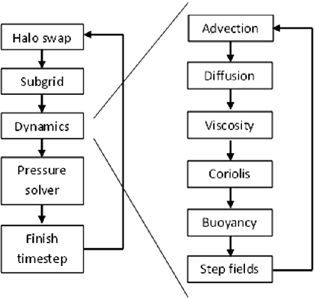
High level structure of a single MONC timestep
2.2 Hardware Setup
For the work described in this paper we are using an ADM8K5 PCI Express card, manufactured by Alpha Data, which mounts a Xilinx Kintex Ultrascale KU115-2 FPGA. This FPGA contains 663,360 LUTs, 5520 DSP48E slices and 4320 BRAM 18K blocks. The card also contains two banks of 8 GB DDR4-2400 SDRAM, external to the FPGA, and a number of other interfaces which are not relevant to this work. Because the FPGA used for this work is part of the Xilinx product family, it is their general ecosystem, including tooling, that we use in this work. However, we believe that the lessons learnt apply more generally to product families of FPGAs from other vendors too.
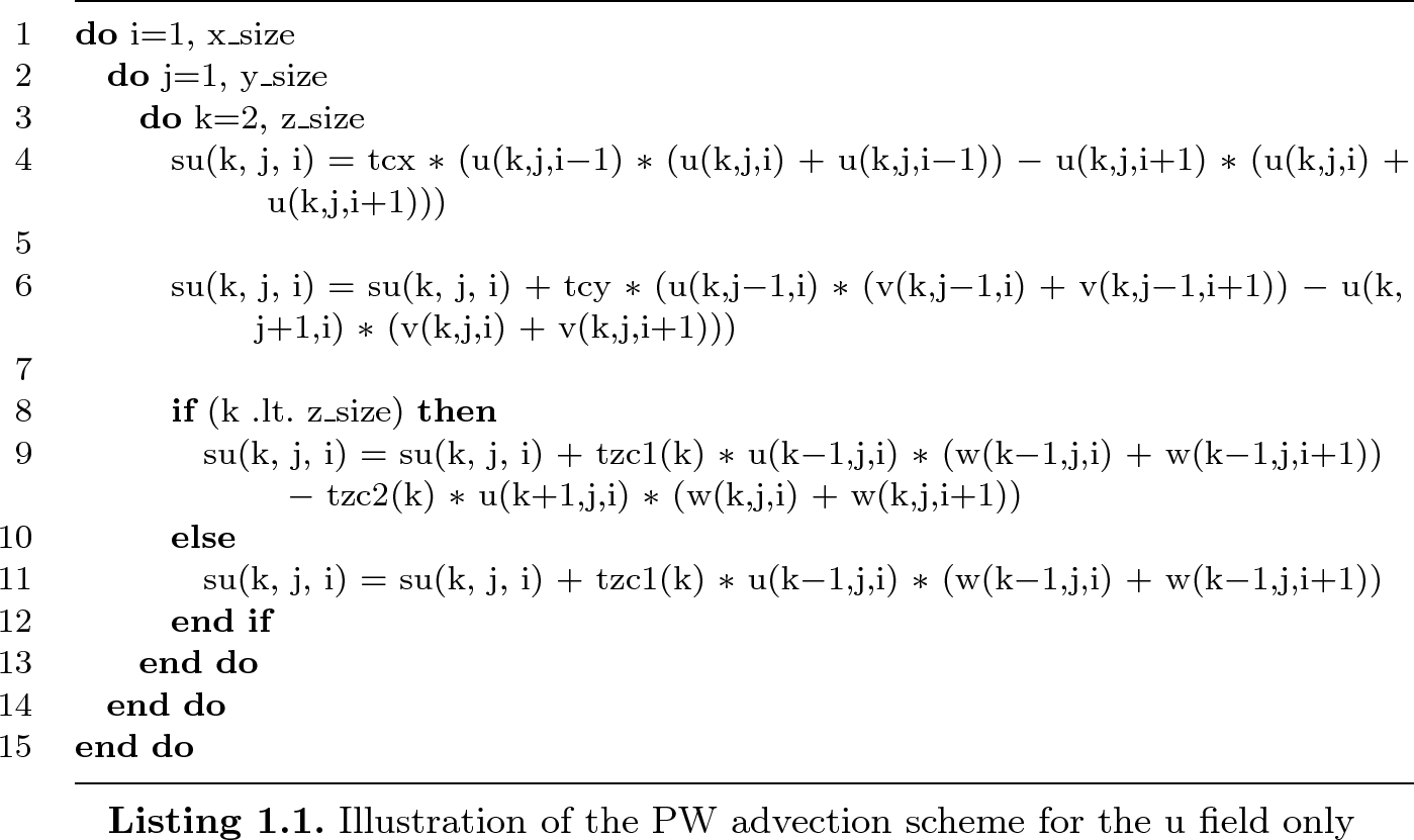
This PCIe card is plugged into an Intel Xeon system, which contains two Sandybridge CPUs, each with four physical cores running at 2.40 GHz, and 32 GB RAM (16 GB per NUMA region). Our approach is to run MONC on the CPU and study the benefit of offloading the PW advection scheme onto the PCIe mounted FPGA. Not only does this involve performing the double precision calculations for all three fields illustrated in Listing 1.1, but also transferring the necessary flow field data onto, and resulting source terms back from, the card. Whilst some FPGAs such as the Zynq use a more embedded style, where typically ARM cores are combined with FPGA fabric on the same chip, we believe this PCIe setup is more interesting in the field of HPC. There are a number of reasons for this, firstly because a powerful Xeon CPU can be used on the host side, secondly because a large amount of memory can be placed close to the FPGA on the PCIe card to handle the processing of large problems, and thirdly because this is a very common accelerator architecture already adopted in HPC GPU systems.
2.3 FPGA Programming Techniques and Our Approach
The traditional approach to programming FPGAs has been to develop codes in a Hardware Description Language (HDL) such as VHDL or Verilog. However, this is a very time consuming process [8] which requires significant expertise and experience. As such, higher level programming tools have been developed to assist in programming, and High Level Synthesis (HLS) is amongst the most prevalent of these. A kernel, written in C, C++ or System C, is automatically translated, via HLS, into the underlying HDL. Driven by pragma style hints provided by the programmer, this substantially speeds up development time and allows for application developers to take advantage of the knowledge and experience of the FPGA vendor. An example of this is in floating point operations, where HLS will automatically include pre-built floating point cores to perform operations, instead of the HDL developer having to develop their own solution.
HLS can be used as a building block of further programming abstractions, and recently the use of OpenCL for programming FPGAs has become popular [9]. Decorating their code via OpenCL abstractions, a tool-chain such as Xilinx’s SDAccel converts this into a form understandable by HLS, then uses HLS to generate the appropriate HDL and integrates this into a wider design based upon a board specific support package. An alternative approach which, in contrast to OpenCL, requires a bit more work on behalf of the programmer, is the use of the high-level productivity design methodology [10]. In this technique, the FPGA is configured using a block design approach, where existing IP blocks are imported and connected together by the programmer. This emphasises the reuse of existing IP and the idea of a shell, providing general foundational functionality that the programmer’s kernel, via an IP block generated by HLS, can be dropped into and easily integrated. By separating the shell from the kernel, the general shell infrastructure can be reused for many different applications, and updating the functionality of the kernel, which is quite common during development, often just requires re-importing the IP block into the board design. This approach also eases testing, as the kernel and shell can be validated separately.
In this work we followed the high-level productivity design methodology, where one explicitly writes a C kernel for HLS, generates the HDL and export this as an IP block. This block is then integrated with a shell, providing the general infrastructure. There were two reasons for adopting this approach, firstly because it gave us more control over the configuration of our design, and we think that some of the lessons learnt for HPC codes could then potentially feed into higher level abstractions, such as those provided by OpenCL. Secondly, we chose this approach because SDAccel, the implementation of OpenCL for Xilinx FPGAs, is an extra commercial product that requires further licencing.

Runtime of the PW advection kernel alone for different steps taken when porting it to HLS for a problem size of x = 512, y = 512, z = 64 (16.7 million grid cells)
3 Developing the PW Advection HLS Kernel
Figure 2 illustrates the performance of our HLS PW advection kernel over numerous steps that we applied one after another, for an experiment of x = 512, y = 512, z = 64 (16.7 million grid cells). We use this table to drive our discussions in this section about the different steps required to optimise an HLS kernel and, for reference, the top entry of Fig. 2, Reference on CPU, illustrates the kernel’s runtime over a single Sandybridge CPU core on the host. Our focus in this section is the HLS kernel alone, and as such we ignore the transferring of data which must occur to the PCIe before the kernel runs and the copying back of data once the kernel has completed. This transferring is considered in more detail in the next section.

We next added the HLS pipeline directive, #pragma HLS PIPELINE II=1, to our inner loop, working up a single column. This instructs HLS to pipeline the processing of the inner loop and II is the initiation interval latency, which instructs HLS how often to add a new element of data to the pipeline, in this case every cycle if possible. HLS takes the inner loop, containing our 53 double precision operations, and breaks this up into individual pipeline stages which can run concurrently. These are then fed with data from the outer loops and, once the pipeline is filled, each stage is running, at the same time, on a different element of data before passing the result to the next stage. From Fig. 2 it can be seen that this significantly decreased the runtime of the kernel, by around five times, but this was still around twenty time slower than running on the CPU.

To address this we duplicated these same arrays, for instance u_vals2 which holds the same data as u_vals. Whilst another way around this in HLS is to use partitioning, effectively splitting the array up across multiple BRAM controllers, due to the dynamic size of the inner loop, we would have been forced to partition the arrays into single elements, and this resulted in worse utilisation and performance. In comparison, duplicating the BRAM array worked well.
It can be seen from Fig. 2 that this local copying of data decreased the runtime by over four times. However, the major disadvantage of the approach in Listing 1.3 is that the outer loops of j in the Y dimension and i in the X dimension are no longer continually feeding data into the pipelined inner loop. Instead, the inner loop runs in a pipelined fashion just for a single column, in this case of maximum 64 data elements, and then must drain and stop, before memory copies into local arrays are performed for the next column. Bearing in mind the pipeline of this inner loop is, as reported by HLS, 71 cycles deep, with an initiation interval, the best HLS can provide, of 2 cycles and assuming a column size of 64 elements, for each column the pipeline will run for 199 cycles but for only 57 of these cycles (28%) is the pipeline full utilised, the rest of the time it is either filling or draining.
To address this we extended our local BRAM arrays to hold data for multiple columns in the Y dimension, extending each array from MAX_VERTICAL_SIZE to MAX_VERTICAL_SIZE * Y_BATCH_SIZE. In this situation the middle loop, j, working in the Y dimension runs in batches, of size Y_BATCH_SIZE. For each batch it will copy the data for Y_BATCH_SIZE columns, and then process each of these columns. The major benefit of this approach is that our pipeline, working up the column in the inner loop, is now fed by Y_BATCH_SIZE columns rather than one single column. Additionally, at this point, HLS reported that it had been able to reduce the initiation interval down from two to one, effectively doubling the performance of the inner loop pipeline. Assuming a Y_BATCH_SIZE of 64 and that the column size is still 64, the pipeline now runs for 4167 cycles, 97% of which the pipeline is fully filled. This represents a significant increase in utilisation, and ultimately performance, because the pipeline is able to process, and hence generate a result, every clock cycle for 97% of the time it is running. As per Fig. 2, this over halved the kernel execution time at the cost of increasing the BRAM usage by over three times.
At this point the individual lines of code for our inner loop kernel, containing the fifty three double precision floating point operations, were still laid out similarly to Listing 1.1, where the calculations for a specific value of the source term were in one line. We had trusted HLS to extract out the individual variable accesses, and structure these appropriately, but we found that actually HLS does a fairly poor job of identifying which variables are shared and hence can be reused between calculations. As such, we significantly restructured the code, splitting up calculations into their individual components of reading data into temporary variables and then using that single variable whenever the value is required in the inner loop. This is the Extract all variables entry of Fig. 2 and had two impacts. Firstly, it reduced the pipeline depth from 71 cycles deep to 65, and hence provided a modest increase in performance, but also it reduced the number of reads on our local arrays and so we were able to remove a number of duplicate local arrays which reduced the overall BRAM usage by around 30%.
When issuing memory copies, for instance in lines 5 to 7 of Listing 1.3, the port must be read which accesses data from external SDRAM, and the same is true in the other direction when writing data. In the default mode, ports will tend to issue an access for every individual element, but instead it is possible to decorate the kernel’s external data array variable definitions (e.g. u and su) with pragmas to instruct HLS to issue bursts of data, retrieving n elements in one go. This is important in our situation because we are never just reading one element at a time, but instead the data for Y_BATCH_SIZE columns. The HLS INTERFACE pragma, as illustrated in Listing 1.2, was modified for our kernel’s external data arrays (e.g. u and su) with the addition of num_read_outstanding=8 num_write_outstanding=8 max_read_burst_length=256 max_write_burst_length=256. This directs HLS to read and write in bursts of size 256, the maximum size, and supports holding up to eight of these bursts at any one time. The latency modifier advises HLS to issue the access before it is needed, in this example around 60 cycles beforehand. HLS uses BRAM to store these bursts and, as can be seen in Fig. 2, resulted in a modest increase in BRAM usage but also a reasonable decrease in execution time.

Until this point we have relied on the use of the memcpy function to copy data from one location to another. However bearing in mind there are multiple copies of local column data arrays due to BRAM port limits, e.g. u_vals and u_vals2, issuing a separate memcpy for each of these when we loop into the next X dimension is quite slow because HLS will not execute these memory copies concurrently. Instead, replacing the memcpy calls with explicit loops, where each index location is read from the source array and then written to each of the target arrays was faster. In fact, more generally we found that replacing all the memcpy calls with an explicitly pipelined loop that performed the copying in user code, was beneficial. This is represented as the Replace memcpy with explicit loops entry of Fig. 2 and it can be seen that not only did we obtain a modest increase in performance, but it also decreased our LUT utilisation slightly.
The default clock on the ADM8K5 board is 250 Mhz, and so a period of 4ns was used initially, with HLS estimating a clock period of 3.75 ns due to limits in double precision multiplication. However, via configuring the HLS floating point kernels it was possible to tune them. Using #pragma HLS RESOURCE variable=a core=DMul_maxdsp latency=14, HLS was instructed to use the DMul_maxdsp double precision floating point core (leveraging DSP slices as much as possible for the double precision multiplication) with a latency of 14 cycles for all multiplications involving the variable a. This latency is the core’s pipeline depth and, by increasing it, it is possible to reduce the minimum clock period. We applied this directive to all variables that are involved in double precision multiplication, and found that the best clock period we could get from the double precision multiplication core was 2.75 ns. Whilst the latency value can go all the way up to twenty, above fourteen made no difference to the period. As such we were able to reduce our clock period to 3.2 (there is a 12.5% clock uncertainty), meaning we could run our kernel at 310Mhz instead of 250Mhz. The pipeline depth has increased from 65 to 72, but due to the increase in clock frequency, the overall latency for data to progress through the pipeline has gone from 2.6e−7 s to 2.3e−7 s, so there is an increase in overall performance.
From Fig. 2 it can be seen that the LUT and DSP48E utilisation dropped very significantly with this last configuration. This was because we also instructed HLS to use the full DSP core when it came to double precision addition and subtraction. It is the use of this core that reduced the LUT usage by around a quarter, and also, ironically, slightly reduced the number of DSP48E slices too.
As a result of the steps applied in this section, we have reduced the runtime of our HLS kernel by over 100 times, from being 75 times slower than running over a single Sandybridge CPU core on the host, to being around a quarter faster, however as noted at the start of the section this is just the kernel execution time and ignores the DMA transfer time needed to get data on and off the board before and after the kernel runs.
4 Putting It All Together, the Block Design

The MONC PW advection board design, containing four of our PW advection HLS kernels and other general infrastructure to support this
Figure 4 provides a more detailed view of the integration of our PW advection kernel IP blocks. For purposes of illustration, we have slightly moved the appropriate IP blocks around, when compared to Fig. 3, so the topical ones are in the same image. On the bottom left of Fig. 4, the ADM PCIe block is the PCIe interface and the four DMA channel ports on the right of this IP block, along with the direct slave port can be clearly seen. The clocking wizard, top left, converts the 250 Mhz reference clock up to 310 Mhz for the PW advection IP blocks as described in Sect. 3. The direct slave interface is connected to the kernel’s control port, and by writing or reading the appropriate bit we can manage the kernels such as starting or tracking progress. This connection goes, via an AXI4 clock converter IP block, to the slave interface of the left most AXI interconnect. This interconnect splits the direct slave data according to its address, the appropriate data then routed to its corresponding PW advection kernel. These addresses are defined in the block design address editor.
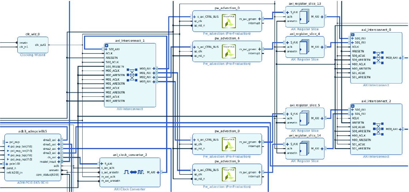
Integration of the PW advection HLS IP blocks in our board design

DMA transfer time for different configurations with a data size of 1.6 GB
5 Performance Comparison
We built the block design described in Sect. 4 with twelve PW advection kernels as described in Sect. 3. In order to fit within the limits of the Kintex FPGA we instructed HLS to use the medium DSP core for double precision multiplication. This resulted in an overall design utilisation of 78.5% of the Kintex’s LUTs, 84.2% BRAM-18k blocks and 89% of the chip’s DSP48E slices. It took around fifteen hours of CPU time to build the entire design, most of which was spent in the place and route phases.
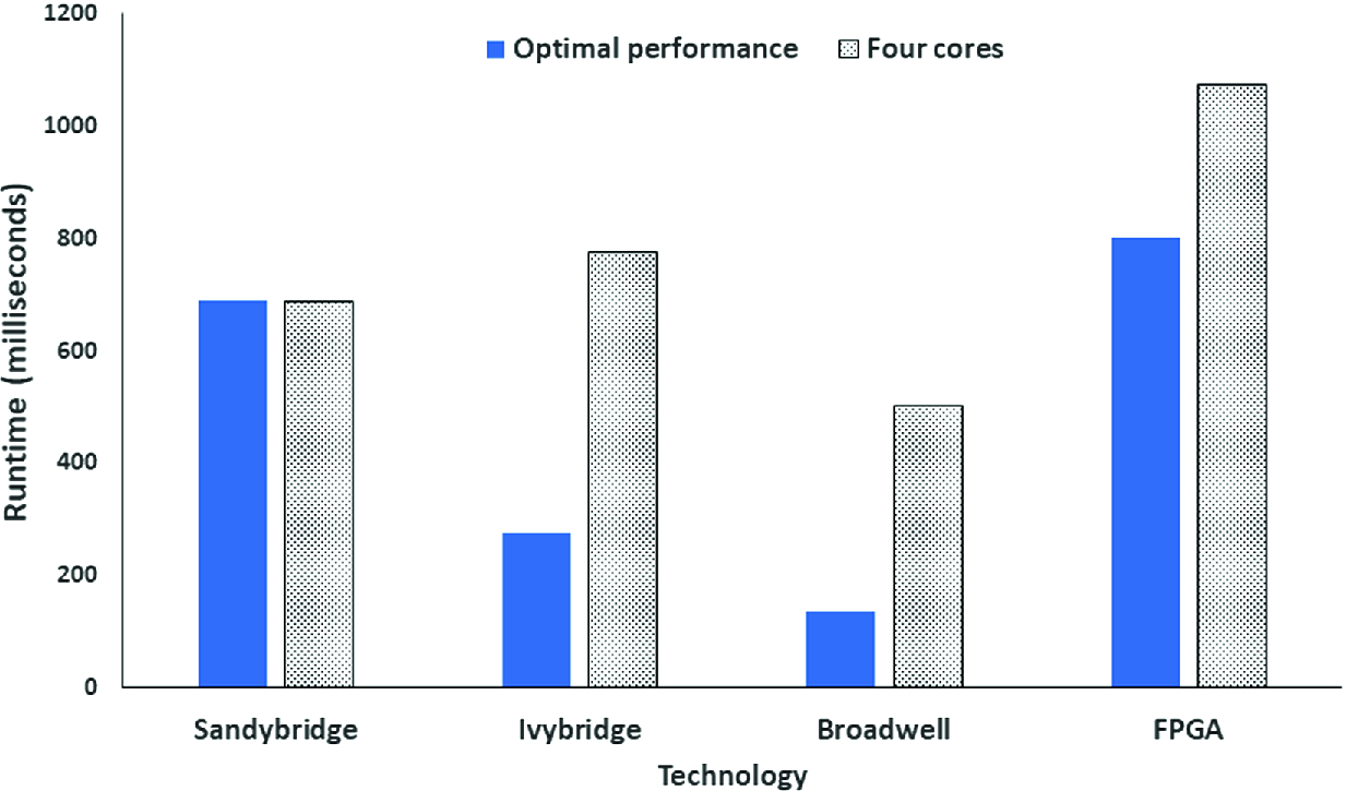
Performance comparison of x = 1012, y = 1024, z = 64 (67 million grid points) with a standard status cloud test-case
It can be seen from Fig. 6 that our optimal FPGA version performs slower in comparison to all CPU products tested and this trend continues when we consider four core performance. This might seem strange seeing that, in Sect. 3, our HLS kernel is faster than running on a single core of Sandybridge and actually is comparable to running on a single core of Broadwell. However, crucially there we were just concerned with the kernel execution time and ignored the DMA transfer time and the results reported in Fig. 6 contain both these aspects.
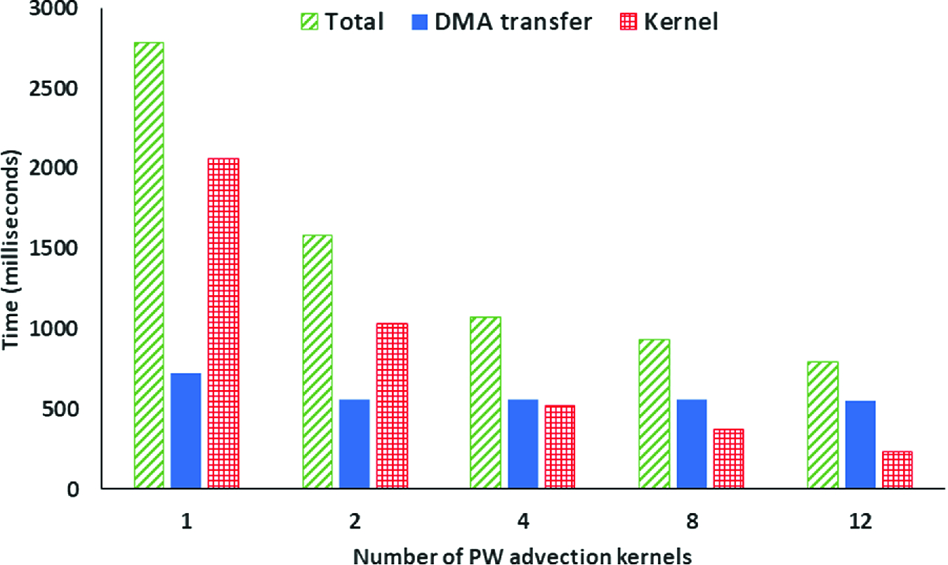
Runtime of different numbers of PW advection kernel broken down into constituent parts when scaling number of kernels, x = 1012, y = 1024, z = 64 (67 million grid cells) with a standard status cloud test-case

Runtime of our FPGA PW advection code (12 kernels) vs Broadwell as we scale the grid size with a standard stratus cloud test-case
6 Conclusions and Further Work
In this paper we have described our approach in porting the PW advection kernel of the MONC atmospheric model onto FPGAs. Using HLS, we explored in detail the different steps required in porting the kernel and how best to structure the board design. We have shown that it is crucial that HPC application developers rethink and recast their code to suit the data-flow pattern, and have demonstrated a 100 times performance difference between code that does not do this and the same functionality, albeit where the code looks very different, tuned for the FPGA. This re-enforces the point that, whilst it is fairly simple for an HPC applications developer to import some C code into HLS and synthesis this, significant work and experimentation is required to get reasonable performance.
When considering only the kernel execution time, our HLS kernel outperformed a single core of Sandbridge and performs comparable with a single Broadwell core. But when including the DMA transfer time we found that this is a very severe limitation of our FPGA design in contrast to the performance one can gain from the same advection kernel threaded over the cores of Intel CPUs commonly found in HPC machines.
When it comes to further work, it is this DMA transfer time that needs to be tackled. At the largest problem size of 268 million grid cells explored in this paper, a total of 12.88 GB needs to be transferred which takes 2.2 s and represents a transfer rate of 5.85 GB/s, which is reasonable based on the specifications of this PCIe card. One idea is to use single rather than double precision, which would effectively halve the amount of data that needs to be transferred, although the DMA transfer time at 134 million grid points is still substantially slower than Broadwell execution time at 268 million grid points. Another idea is to chunk up the DMA transfer, starting the appropriate PW advection kernel as soon as the applicable chunk has arrived rather than all the data, this could be driven by a host thread or extra logic in the block design.
There is also further exploration that can be done based on our HLS kernel and one aspect would be to look at how best to further increase the clock speed. The 2.8 ns period of the double precision multiply currently limits us to 310 Mhz, but replacing double precision with single or fixed point could enable higher clock frequencies and single precision would also halve the amount of data transferred from SDRAM to the kernels. This last point is important, because we believe that SDRAM access time is now the major source of overhead in our HLS kernel.
Therefore, we conclude that, whilst FPGAs are an interesting and generally speaking viable technology for accelerating HPC kernels, there is still work to be done to obtain performance competitive to modern day Intel CPUs. When running large system sizes on PCIe mounted FPGAs, the cost of transferring data to and from the card can be very significant and severely limits performance. This is important to bear in mind and, going forwards, if we can address these limits then we feel that FPGAs will become a much more competitive approach.
Acknowledgements
The authors would like to thank Alpha Data for the donation of the ADM8K5 PCIe card used throughout the experiments of work. This work was funded under the EU FET EXCELLERAT CoE, grant agreement number 823691.