10.1 What Is “High Resolution SEM Imaging”?
“I know high resolution when I see it, but sometimes it doesn’t seem to be achievable!”
“High resolution SEM imaging” refers to the capability of discerning fine-scale spatial features of a specimen. Such features may be free-standing objects or structures embedded in a matrix. The definition of “fine-scale” depends on the application, which may involve sub-nanometer features in the most extreme cases. The most important factor determining the limit of spatial resolution is the footprint of the incident beam as it enters the specimen. Depending on the level of performance of the electron optics, the limiting beam diameter can be as small as 1 nm or even finer. However, the ultimate resolution performance is likely to be substantially poorer than the beam footprint and will be determined by one or more of several additional factors: (1) delocalization of the imaging signal, which consists of secondary electrons and/or backscattered electrons, due to the physics of the beam electron ̶ specimen interactions; (2) constraints imposed on the beam size needed to satisfy the Threshold Equation to establish the visibility for the contrast produced by the features of interest; (3) mechanical stability of the SEM; (4) mechanical stability of the specimen mounting; (5) the vacuum environment and specimen cleanliness necessary to avoid contamination of the specimen; (6) degradation of the specimen due to radiation damage; and (7) stray electromagnetic fields in the SEM environment. Recognizing these factors and minimizing or eliminating their impact is critical to achieving optimum high resolution imaging performance. Because achieving satisfactory high resolution SEM often involves operating at the performance limit of the instrument as well as the technique, the experience may vary from one specimen type to another, with different limiting factors manifesting themselves in different situations. Most importantly, because of the limitations on feature visibility imposed by the Threshold Current/Contrast Equation, for a given choice of operating conditions, there will always be a level of feature contrast below which specimen features will not be visible. Thus, there is always a possible “now you see it, now you don’t” experience lurking when we seek to operate at the limit of the SEM performance envelope.
10.2 Instrumentation Considerations
High resolution SEM requires that the instrument produce a finely focused, astigmatic beam, in the extreme 1 nm or less in diameter, that carries as much current as possible to maximize contrast visibility. This challenge has been solved by different vendors using a variety of electron optical designs. The electron sources most appropriate to high resolution work are (1) cold field emission, which produces the highest brightness among possible sources (e.g., ~109 A/(cm2sr−1) at E 0 = 20 keV) but which suffers from emission current instability with a time constant of seconds to minutes and (2) Schottky thermally assisted field emission, which produces high brightness (e.g., ~108 A/(cm2sr−1) at E 0 = 20 keV) and high stability both over the short term (seconds to minutes) and long term (hours to days).
10.3 Pixel Size, Beam Footprint, and Delocalized Signals
The fundamental step in recording an SEM image is to create a picture element (pixel) by placing the focused beam at a fixed location on the specimen and collecting the signal(s) generated by the beam–specimen interaction over a specific dwell time. The pixel is the smallest unit of information that is recorded in the SEM image. The linear distance between adjacent pixels (the pixel pitch) is the length of edge of the area scanned on the specimen divided by the number of pixels along that edge. As the magnification is increased at fixed pixel number, the area scanned on the specimen decreases and the pixel pitch decreases. Each pixel represents a unique sampling of specimen features and properties, provided that the signal(s) collected is isolated within the area represented by that pixel. “Resolution” means the capability of distinguishing changes in specimen properties between contiguous pixels that represent a fine-scale feature against the adjacent background pixels or against pixels that represent other possibly similar nearby features. Resolution degrades when the signal(s) collected delocalizes out of the area represented by a pixel into the area represented by adjacent pixels so that the signal no longer exclusively samples the pixel of interest. Signal delocalization has two consequences, the loss of spatial specificity and the diminution of the feature contrast, which affects visibility. Thus, when the lateral leakage becomes sufficiently large, the observer will perceive blurring, and less obviously the feature contrast will diminish, possibly falling below the threshold of visibility.
Relationship between nominal magnification and pixel dimension
Nominal magnification (10 × 10-cm display) | Edge of scanned area (μm) | Pixel pitch (1000 x 1000-pixel scan) |
|---|---|---|
40× | 2500 | 2.5 μm |
100× | 1000 | 1 μm |
200× | 500 | 500 nm |
400× | 250 | 250 nm |
1000× | 100 | 100 nm |
2000× | 50 | 50 nm |
4000× | 25 | 25 nm |
10,000× | 10 | 10 nm |
20,000× | 5 | 5 nm |
40,000× | 2.5 | 2.5 nm |
100,000× | 1 | 1 nm |
200,000× | 0.5 | 500 pm |
400,000× | 0.25 | 250 pm |
1,000,000× | 0.1 | 100 pm |
Diameter of the area at the surface from which 90 % of BSE (SE3) and SE2 emerge
E 0 | C | Cu | Au |
|---|---|---|---|
30 keV | 11.8 µm | 2.6 µm | 1.2 µm |
20 keV | 6.0 µm | 1.4 µm | 590 nm |
10 keV | 1.9 µm | 410 nm | 180 nm |
5 keV | 590 nm | 130 nm | 58 nm |
2 keV | 128 nm | 28 nm | 12 nm |
1 keV | 41 nm | 8.8 nm | 3.9 nm |
0.5 keV | 12.7 nm | 2.8 nm | 1.2 nm |
0.25 keV | 4.0 nm | 0.9 nm | 0.39 nm |
0.1 keV | 0.86 nm | 0.19 nm | 0.08 nm |

Aluminum-copper eutectic alloy, directionally solidified. The phases are CuAl2 and an Al(Cu) solid solution. Beam energy = 20 keV. a Two-segment semiconductor BSE detector, sum mode (A + B). b Everhart–Thornley detector(positive bias)
10.4 Secondary Electron Contrast at High Spatial Resolution


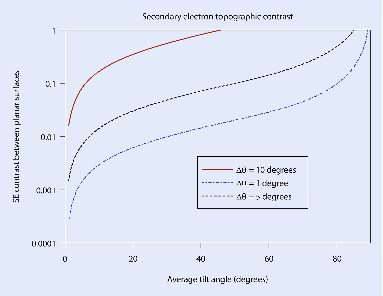
Plot of secondary electron topographic contrast between two flat surfaces with a difference in tilt angle of 1°, 5°, and 10°
- 1.When the beam strikes nearly tangentially, that is, grazing incidence when θ approaches 90° and sec θ reaches very high values, as the beam travels near the surface and a high SE signal is produced, an effect that is seen in the calculated contrast at high tilt angles in ◘ Figs. 10.2 and 10.3 show an example of a group of particles imaged with an E–T(positive bias) detector. High SE signals occur where the beam strikes the edges of the particles at grazing incidence, compared to the interior of the particles where the incidence angle is more nearly normal.
 Fig. 10.3
SEM image of SRM 470 (Glass K -411) micro-particles prepared with an Everhart–Thornley detector(positive bias) and E 0 = 20 keV. Note bright edges where the beam strikes tangentially
- 2.
At feature edges, especially edges that are thin compared to the primary electron range. These mechanisms result in a very noticeable “bright edge effect.”
10.4.1 SE Range Effects Produce Bright Edges (Isolated Edges)

Schematic diagram showing behavior of BSE and SE signals as the beam approaches a vertical edge

a SEM image at E 0 = 5 keV of TiO2 particles using a through-the-lens detector for SE1 and SE2 (Bar = 100 nm). b Note bright edge effects and convergence of bright edges for the smallest particles (Example courtesy John Notte, Zeiss)
10.4.2 Even More Localized Signal: Edges Which Are Thin Relative to the Beam Range

Schematic diagram of the enhanced BSE and SE production at an edge thin enough for beam penetration. BSEs may strike multiple surfaces, creating several generations of SEs
10.4.3 Too Much of a Good Thing: The Bright Edge Effect Can Hinder Distinguishing Shape

Convergence of bright edges as feature dimensions approach the SE escape distance. a Object edges separated by several multiples of the SE escape distance so that edge effects are distinct; b object edges sufficiently close for edge effects to begin to merge
10.4.4 Too Much of a Good Thing: The Bright Edge Effect Hinders Locating the True Position of an Edge for Critical Dimension Metrology
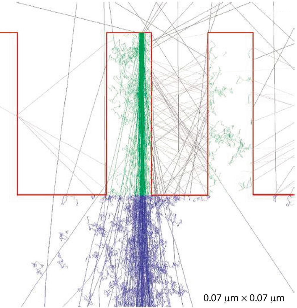
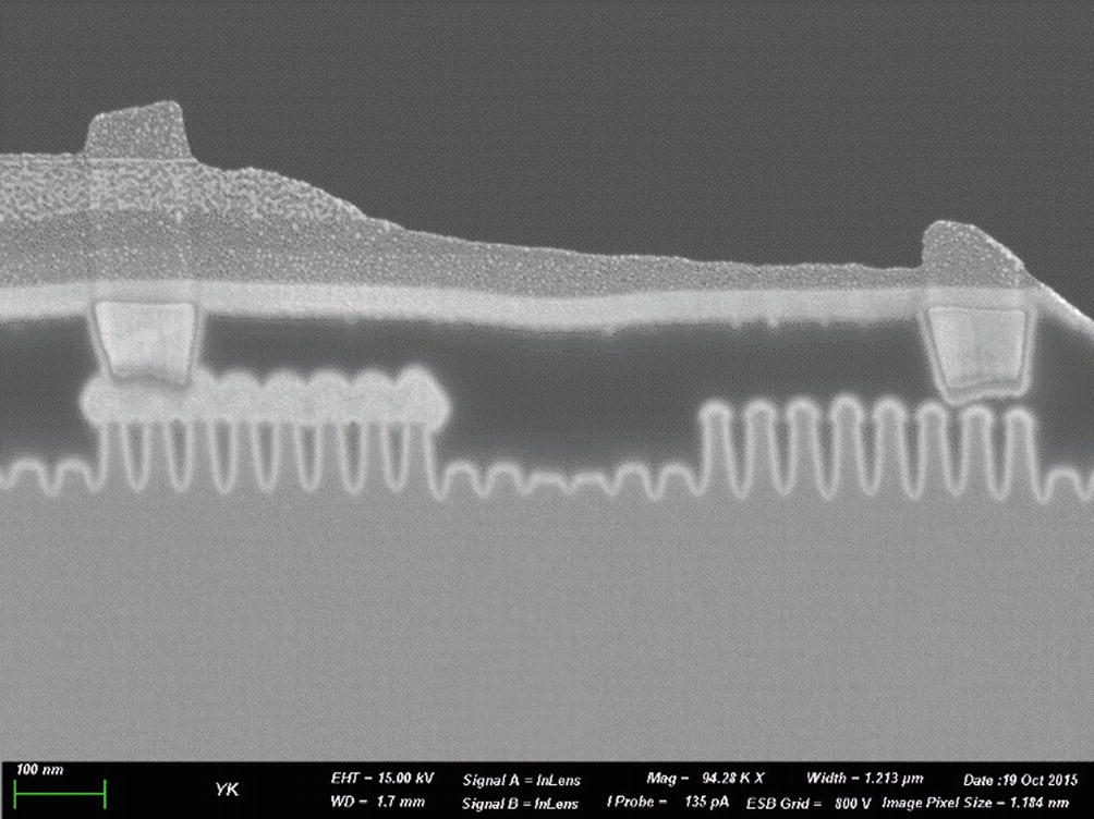
Monte Carlo electron trajectory simulation of complex interactions at line-width structures as calculated with the J-MONSEL code (Villarrubia et al. 2015)
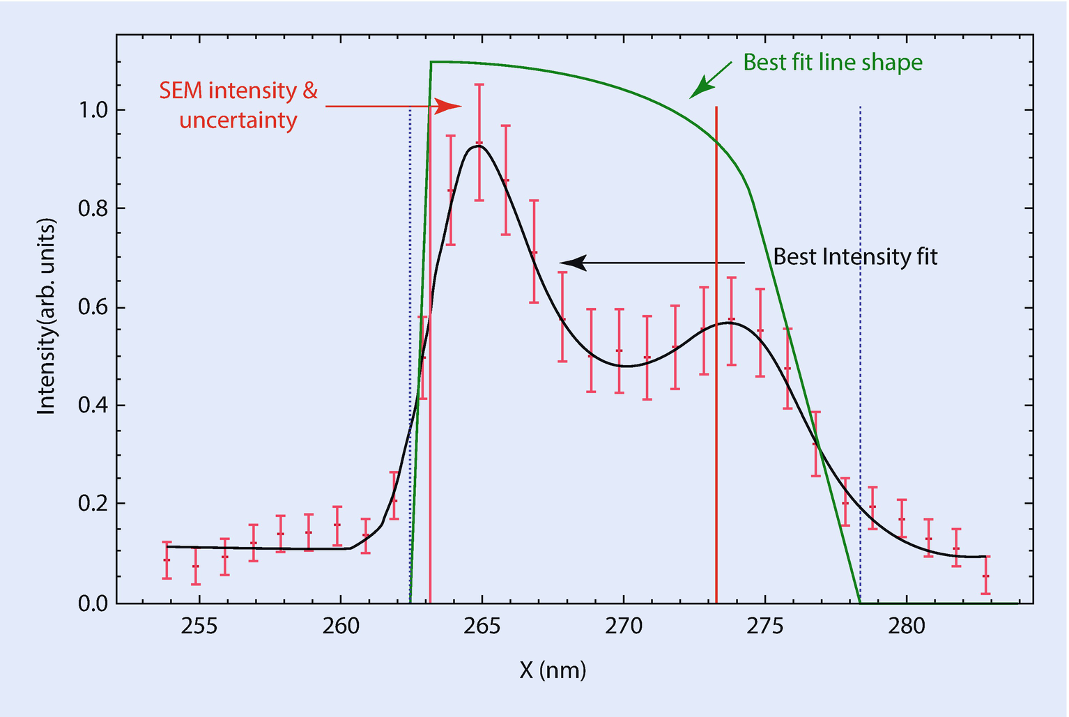
Application of J-MONSEL Monte Carlo simulation to measured SEM profile data and the estimated shape that best fits the data (Villarrubia et al. 2015)

a Top-down SEM image of line-width test structures; E 0 = 15 keV. b Side view of structures revealed by focused ion beam milling showing estimated shape from modeling of the top-down image (red trace) compared with the edges directly found in the cross sectional image (blue) (Villarrubia et al. 2015)
10.5 Achieving High Resolution with Secondary Electrons
Type 1 secondary electrons (SE1), which are generated within the footprint of the incident beam and from the SE escape depth of a few nanometers, constitute an inherently high spatial resolution signal. SE1 are capable of responding to specimen properties with lateral dimensions equal to the beam size as it is made progressively finer. Unfortunately, with the conventional Everhart–Thornley (positive bias) detector, the SE1 are difficult to distinguish from the SE2 and SE3 signals which are created by the emerging BSEs, which effectively carry BSE information, and which are thus subject to the same long range spatial delocalization as BSEs. Strategies to improve high resolution imaging with SEs seek to modify the spatial characteristics and/or relative abundance of the SE2 and SE3 compared to the SE1.
10.5.1 Beam Energy Strategies

a Schematic diagram of the SE1 and SE2 spatial distributions for an intermediate beam energy, e.g., E 0 = 5–10 keV. b Schematic diagram of the SE1 and SE2 spatial distributions for low beam energy, e.g., E 0 = 1 keV. c Schematic diagram of the SE1 and SE2 spatial distributions for high beam energy, e.g., E 0 = 30 keV
10.5.1.1 Low Beam Energy Strategy
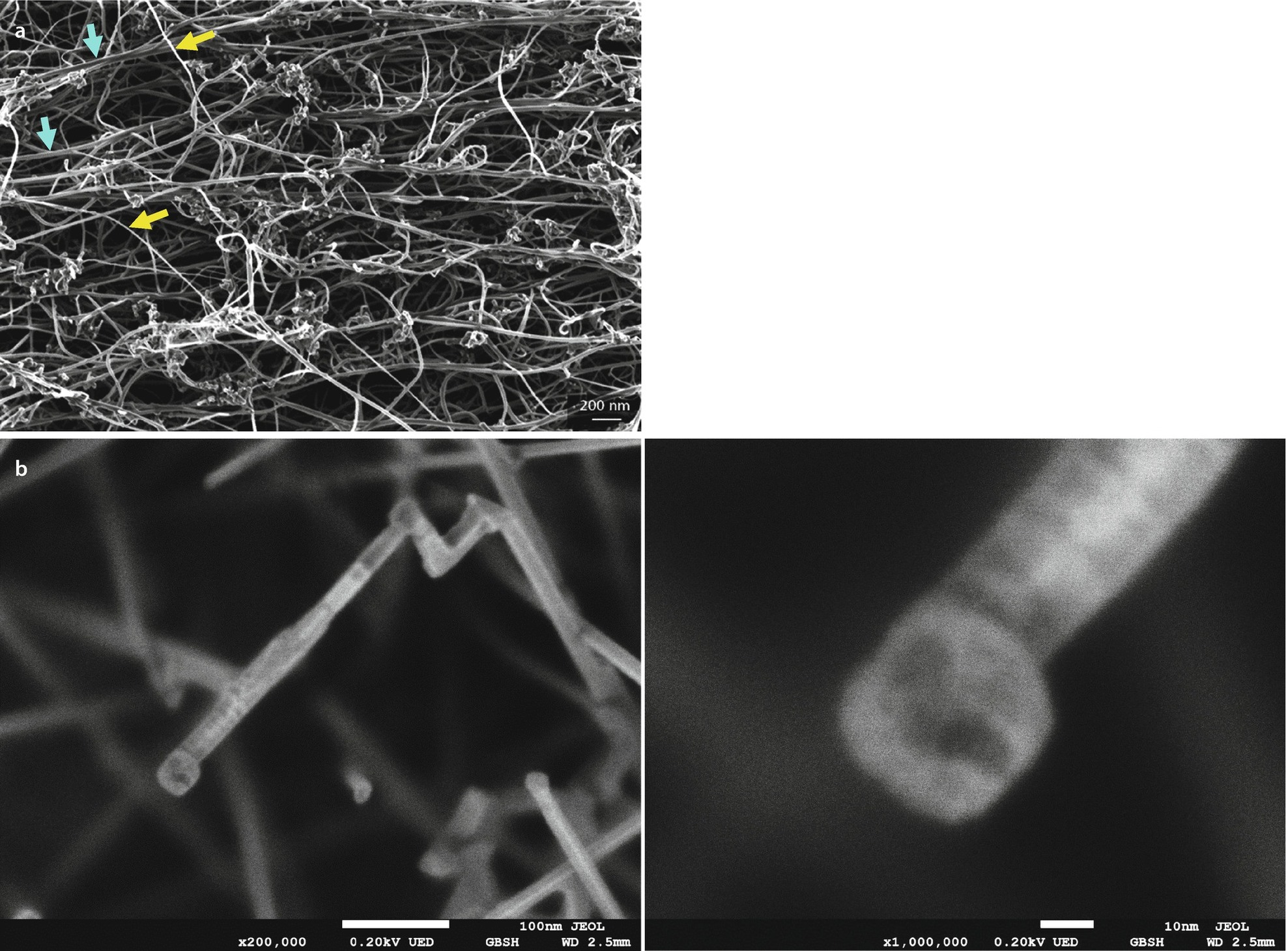
a High resolution achieved at low beam energy, E 0 = 1 keV: image of carbon nanofibers. Note broad fibers (cyan arrows) with bright edges and darker interiors and thin fibers (yellow arrows) for which the bright edge effects converge (Bar = 200 nm) (Example courtesy John Notte, Zeiss). b High spatial resolution achieved at low landing energy: SnO2 whisker imaged with a landing energy of 0.2 keV (left, Bar = 100 nm) (right, Bar = 10 nm) (Images courtesy V. Robertson, JEOL)
By applying a negative potential to the specimen, the landing energy can be reduced even further while preserving high spatial resolution, as shown in ◘ Fig. 10.12b for tin oxide whiskers imaged with a TTL SE detector at a landing energy of E 0 = 0.2 keV.
There are limitations of low beam energy operation that must be acknowledged (Pawley 1984). An inevitable consequence of low beam energy operation is the linear reduction in source brightness, which reduces the current that is contained in the focused probe which in turn affects feature visibility. Low energy beams are also more susceptible to interference from outside sources of electromagnetic radiation.
10.5.1.2 High Beam Energy Strategy
High resolution achieved at high beam energy, E 0 = 15 keV: finFET transistor (16-nm technology) using the in lens SE detector in the Zeiss Auriga Cross beam. This cross section was prepared by inverted Ga FIB milling from backside (Bar = 100 nm) (Image courtesy of John Notte, Carl Zeiss)
10.5.2 Improving the SE1 Signal
Since the SE1 Signal Is So Critical To Achieving High Resolution, What Can Be Done To Improve It?
10.5.2.1 Excluding the SE3 Component
For a bulk specimen, the high resolution SE1 component only forms 5–20 % of the total SE signal collected by the E–T(positive bias) detector, while the lower resolution SE2 and SE3 components of roughly similar strength form the majority of the SE signal. While the SE1 and SE2 components are generated within 1 to 10 μm, the SE3 are produced millimeters to centimeters away from the specimen when the BSEs strike instrument components. This substantial physical separation is exploited by the class of “through-the-lens” (TTL) detectors, which utilize the strong magnetic field of the objective lens to capture the SE1 and SE2 which travel up the bore of the lens and are accelerated onto a scintillator-photomultiplier detector. Virtually all of the SE3 are excluded by their points of origin being outside of the lens magnetic field. For an SE1 component of 10 % and SE2 and SE3 components of 45 %, the ratio of high resolution/low resolution signals thus changes from 0.1 for the E–T(positive bias) detector to 0.22 for the TTL detector.
10.5.2.2 Making More SE1: Apply a Thin High-δ Metal Coating

Schematic illustration of the effect of heavy metal, high δ coating to increase contrast from low-Z targets: a SE signal trace from an uncoated particle; b signal trace after coating with thin Au-Pd
10.5.2.3 Making Fewer BSEs, SE2, and SE3 by Eliminating Bulk Scattering From the Substrate

a Schematic illustration of specimen mounting strategy to minimize background by eliminating the bulk substrate. b Scanning transmission electron microscopy (STEM) two component detector for high energy electrons: on-axis bright-field detector and surrounding annular dark-field detector

SEM imaging glass shards deposited on a thin (~ 10-nm carbon) at E 0 = 20 keV and placed over a deep blind hole in a carbon block
10.5.2.4 Scanning Transmission Electron Microscopy in the Scanning Electron Microscope (STEM-in-SEM)

Dark-field annular detector STEM image of BaFe12O19 nanoparticles; E 0 = 22 keV using oriented dark-field detector in the Zeiss Gemini SEM. The 1.1-nm (002) lattice spacing is clearly evident (Image courtesy of John Notte, Carl Zeiss. Image processed with ImageJ-Fiji CLAHE function)

Schematic cross section of a STEM-in-SEM detector that makes use of the Everhart–Thornley(positive bias) detector to form a bright-field STEM image

Aerosol contamination particles deposited on lacey-carbon film and simultaneously imaged with a TTL detector for SE1 and the STEM-in-SEM detector shown in ◘ Fig. 10.18 (Example courtesy John Small, NIST)
10.5.3 Eliminate the Use of SEs Altogether: “Low Loss BSEs“
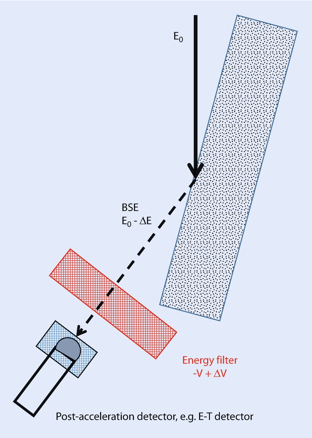
Schematic illustration of low loss BSE imaging from a highly tilted specimen using an energy filter

SE (upper) and low loss BSE (lower) images of photoresist at E 0 = 2 keV. Note the enhanced detail visible on the surface of the LL-BSE image compared to the SE image (Postek et al. 2001)
While the example in ◘ Fig. 10.21 illustrates the utility of LL BSE imaging at low beam energy, LL BSE imaging also enables operation of the SEM at high beam energy (Wells 1971), thus maximizing the electron gun brightness to enable a small beam with maximum current. Low loss images provide both high lateral spatial resolution and a shallow sampling depth.
10.6 Factors That Hinder Achieving High Resolution
10.6.1 Achieving Visibility: The Threshold Contrast

10.6.2 Pathological Specimen Behavior
The electron dose needed for high resolution SEM even with an optimized instrument can exceed the radiation damage threshold for certain materials, especially “soft” materials such as biological materials and other weakly bonded organic and inorganic substances. Damage may be readily apparent in repeated scans, especially when the magnification is lowered after recording an image. If such specimen damage is severe, a “minimum-dose” strategy may be necessary, including such procedures as focusing and optimizing the image on a nearby area, blanking the beam, translating the specimen to an unexposed area, and then exposing the specimen for a single imaging frame.

10.6.3 Pathological Specimen and Instrumentation Behavior
10.6.3.1 Contamination
A modern SEM that is well maintained should not be the source of any contamination that is observed. The first requirement of avoiding contamination is a specimen preparation protocol that minimizes the incorporation of or retention of contaminating compounds when processing the specimen. This caution includes the specimen as well as the mounting materials such as sticky conductive tape. A specimen airlock that minimizes the volume brought to atmosphere for specimen exchange as well as providing the important capability of pre-pumping the specimen to remove volatile compounds prior to insertion in the specimen chamber is an important capability for high resolution SEM. The specimen airlock can also be equipped with a “plasma cleaner” that generates a low energy oxygen ion stream for destruction and removal of organic compounds that produce contamination. If contamination is still observed after a careful preparation and insertion protocol has been followed, it is much more likely that the source of contamination remains the specimen itself and not the SEM vacuum system.
10.6.3.2 Instabilities
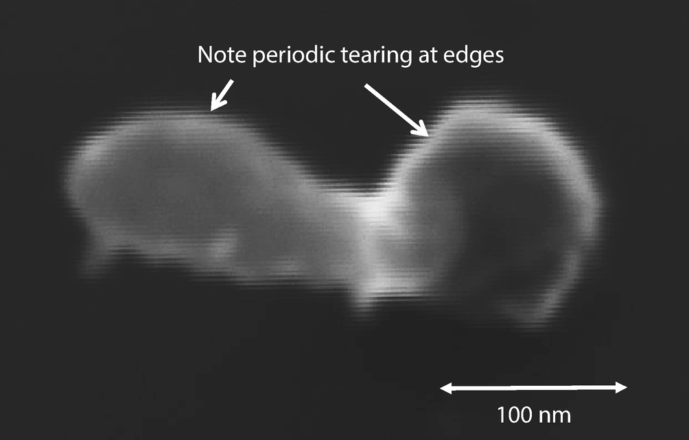
SEM image of nanoparticles showing tearing at the particle edges caused by some source of electromagnetic interference whose frequency is constant and apparently locked to the 60 Hz AC power

Open Access This chapter is licensed under the terms of the Creative Commons Attribution-NonCommercial 2.5 International License (http://creativecommons.org/licenses/by-nc/2.5/), which permits any noncommercial use, sharing, adaptation, distribution and reproduction in any medium or format, as long as you give appropriate credit to the original author(s) and the source, provide a link to the Creative Commons license and indicate if changes were made.
The images or other third party material in this chapter are included in the chapter's Creative Commons license, unless indicated otherwise in a credit line to the material. If material is not included in the chapter's Creative Commons license and your intended use is not permitted by statutory regulation or exceeds the permitted use, you will need to obtain permission directly from the copyright holder.