22.1 What Constitutes “Low” Beam Energy X-Ray Microanalysis?


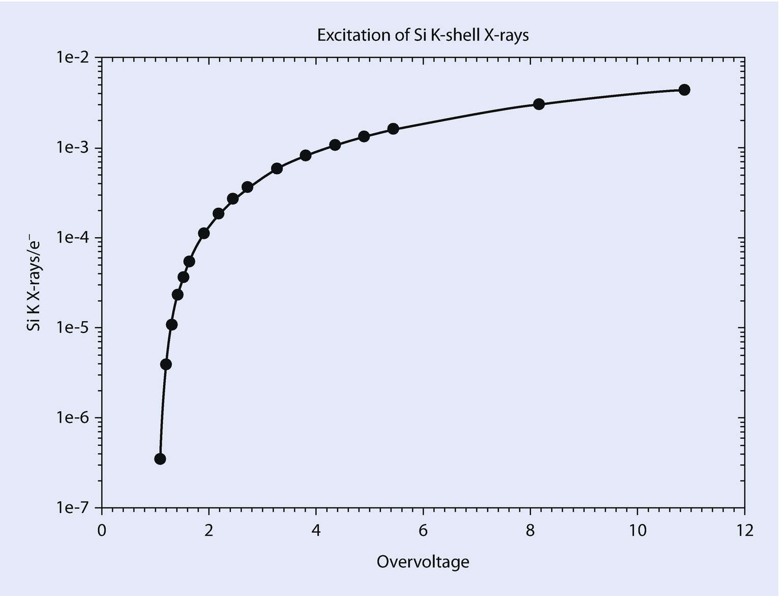
Production of silicon K-shell X-rays with overvoltage
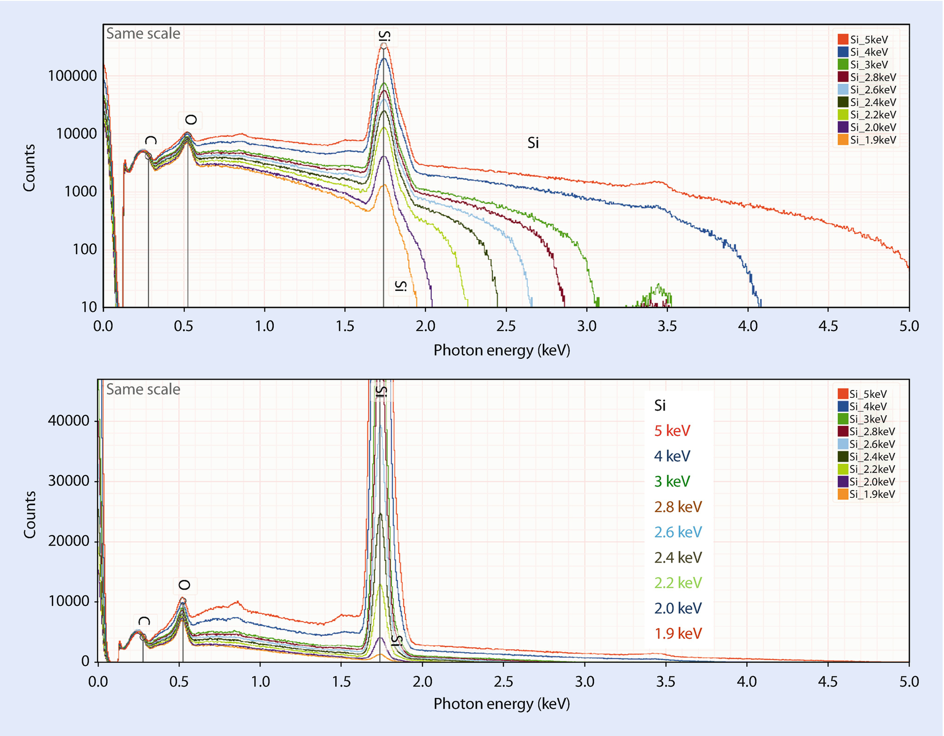
Silicon at various incident beam energies from 5 keV to 1.9 keV showing the decrease in the peak-to-background with decreasing overvoltage

Periodic table illustrating X-ray shell choices for developing analysis strategy within the conventional beam energy range, E 0 = 20 keV (Newbury and Ritchie, 2016)
Periodic table illustrating X-ray shell choices for developing analysis strategy at the lower end of the conventional beam energy range, E 0 = 10 keV (Newbury and Ritchie, 2016)

Periodic table illustrating X-ray shell choices for developing analysis strategy for the upper end of the low beam energy range, E 0 = 5 keV (Newbury and Ritchie, 2016)
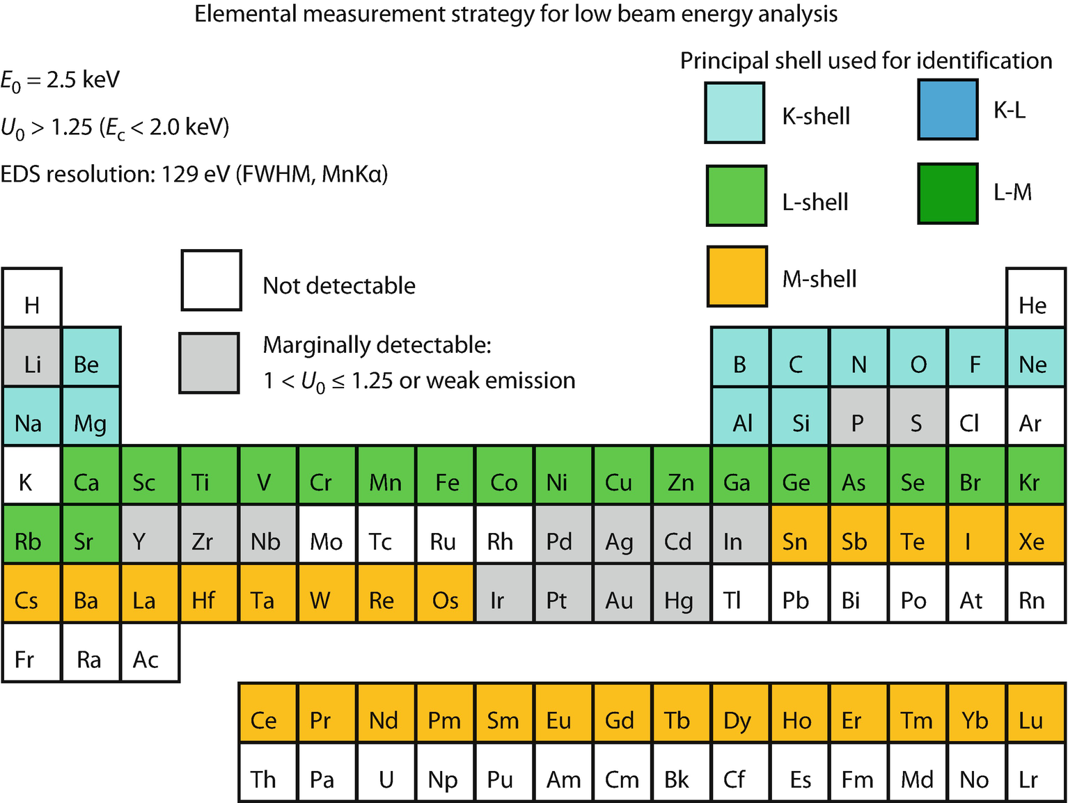
Periodic table illustrating X-ray shell choices for developing analysis strategy within the low beam energy range, E 0 = 2.5 keV (Newbury and Ritchie, 2016)
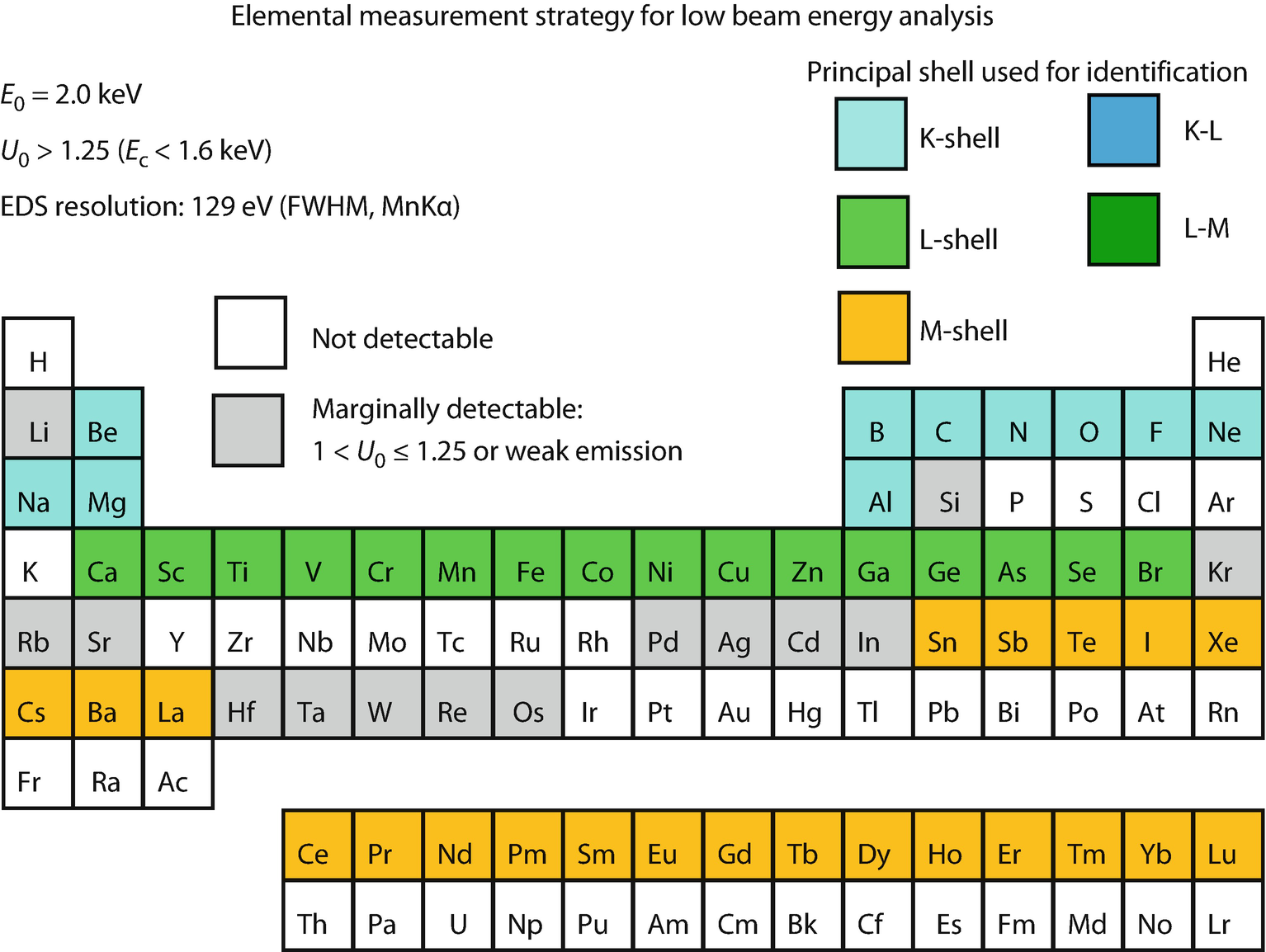
Periodic table illustrating X-ray shell choices for developing analysis strategy within the low beam energy range, E 0 = 2.0 keV (Newbury and Ritchie, 2016)
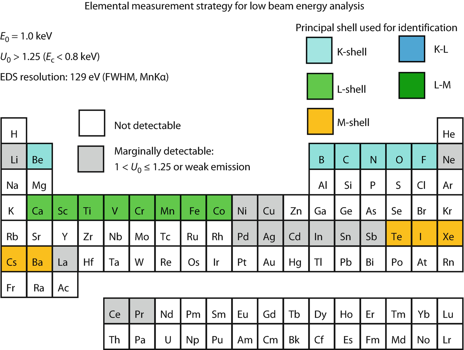
Periodic table illustrating X-ray shell choices for developing analysis strategy within the low beam energy range, E 0 = 1.0 keV (Newbury and Ritchie, 2016)
22.1.1 Characteristic X-ray Peak Selection Strategy for Analysis
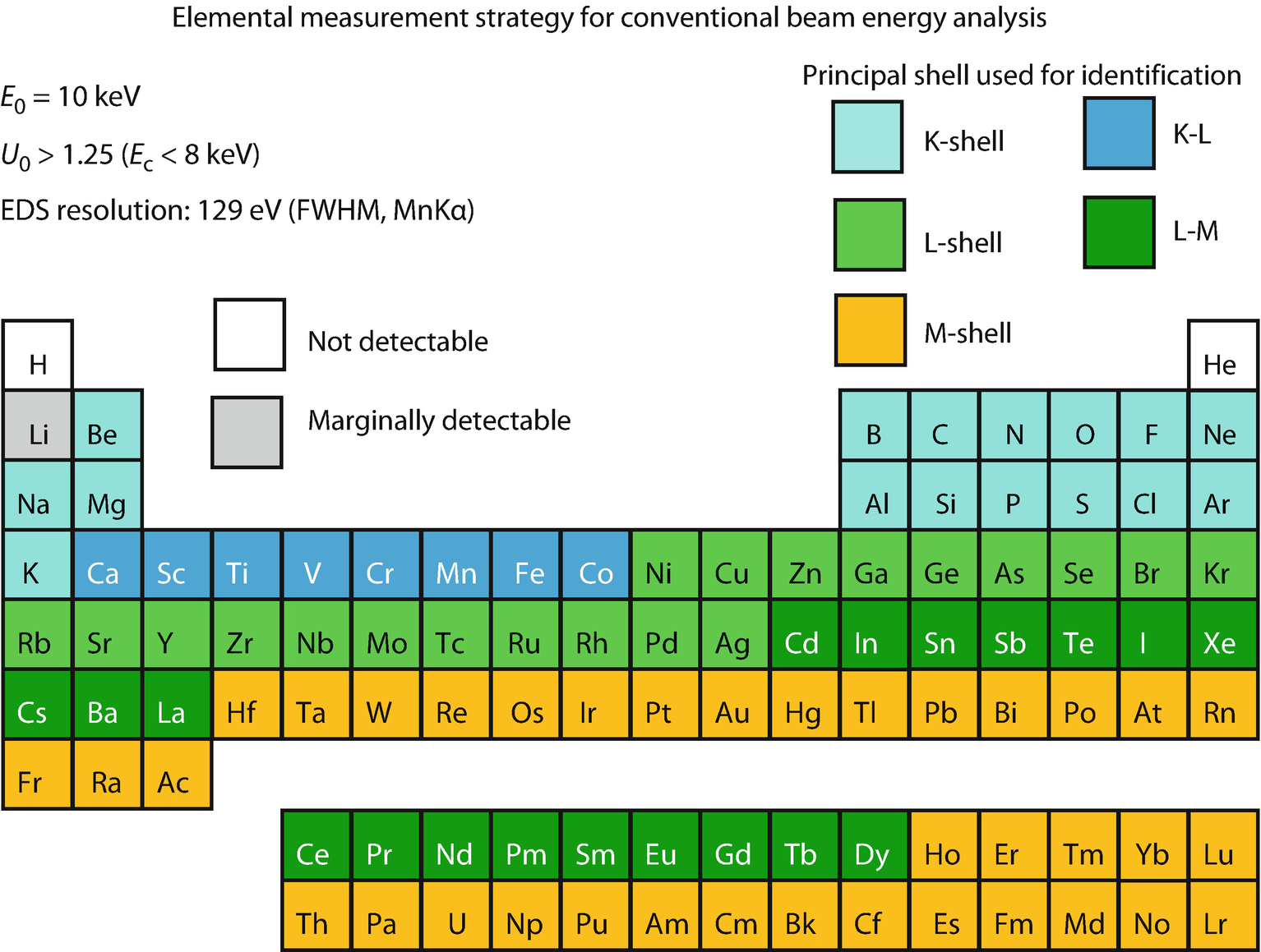
“Conventional” electron-excited X-ray microanalysis is typically performed with an incident beam energy selected between 10 keV and 30 keV. A beam energy is this range is capable of exciting X-rays from one or more atomic shells for all elements of the periodic table, except for hydrogen and helium, which do not produce characteristic X-ray emission. Li can produce X-ray emissions, but the energy of 0.052 keV is below the practical detection limit of most EDS systems, which typically have a threshold of approximately 0.1 keV. Recent progress in silicon drift detector (SDD)-EDS detector technology and isolation windows is rapidly improving the EDS performance in the photon energy range 50 eV – 250 eV, raising the measurement situation for Li from “undetectable” to the level of “marginally detectable.” The choices available for the characteristic X-ray peaks to analyze various elements are illustrated in the periodic table shown in ◘ Fig. 22.3 for E 0 = 20 keV. In constructing this diagram, the assumption has been made with the requirement that U 0 > 1.25 (E c < 16 keV) to provide for robust detection of major and minor constituents. Note that in constructing ◘ Fig. 22.3, only the excitation of characteristic X-rays has been considered and not the subsequent absorption of X-rays during propagation through the specimen to reach the detector. Absorption has a strong effect on low energy X-rays below 2-keV photon energy and strongly depends on composition and beam energy. Absorption can be minimized by operating at low beam energy, as discussed below, an important factor that must also be considered when developing practical X-ray measurement strategy.
As seen in ◘ Fig. 22.3, when the beam energy is selected at the high end of the conventional range, X-rays from two different atomic shells can be excited for many elements, and the additional information provided by having two X-ray families with two or more peaks to identify greatly increases the confidence that can be placed in an elemental identification. This is especially valuable when peak interference occurs between two elements. For example, a severe interference occurs between S K-L2,3 (2.307 keV) and Mo L3-M4,5 (2.293 keV), which are separated by 14 eV. To confirm the presence of Mo when S may also be present, operation with E 0 > 25 keV (U 0 = 1.25) will also excite Mo K-L2,3 (17.48 keV) for unambiguous identification of Mo.
When the beam energy is lowered to the bottom of the conventional analysis range, E 0 = 10 keV, the available X-ray shells for measurement are reduced as shown in ◘ Fig. 22.4. Many more elements can only be analyzed with X-rays from one shell, for example, the Ni to Rb L-shells and the Hf to U M-shells.
22.1.2 Low Beam Energy Analysis Range
When the incident beam energy is reduced to E 0 = 5 keV, further reduction in the atomic shells that can be excited creates the situation shown in ◘ Fig. 22.5. At 5 keV, only one shell is available for all elements except Ca, Cd, In, and Sn. When the incident energy is reduced below 5 keV, some elements are effectively rendered analytically inaccessible by the restrictions imposed by the X-ray physics. The progressive loss of access to elements in the periodic table is illustrated for E 0 = 2.5 keV (◘ Fig. 22.6), E 0 = 2 keV (◘ Fig. 22.7), and E 0 = 1 keV (◘ Fig. 22.8). Indeed, even with E 0 = 5 keV, several elements must be measured with X-rays from shells with low fluorescence yield, such as the Ti L-family and the Ba M-family, resulting in poor peak-to-background.
Based upon the restrictions imposed by the physics of X-ray generation, E 0 = 5 keV is the lowest energy which still gives access to the full periodic table, except for H and He, and therefore this value will be considered as the upper bound of the beam energy range for low beam energy microanalysis. The beam energy range from 5 keV to 10 keV represents the transition region between low beam energy microanalysis and conventional X-ray microanalysis.
22.2 Advantage of Low Beam Energy X-Ray Microanalysis
22.2.1 Improved Spatial Resolution

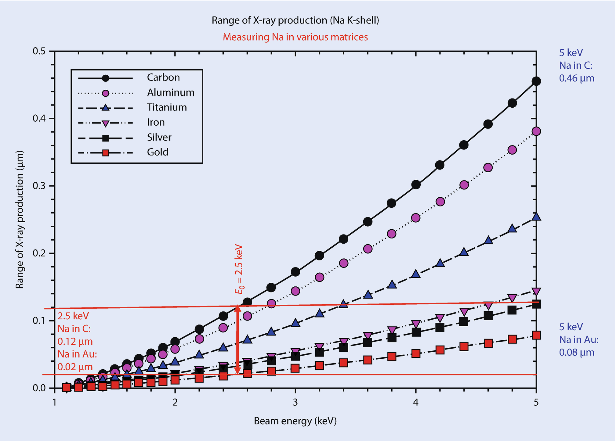
Range of production of Na K-shell X-rays in various matrices, as calculated with the Kanaya–Okayama range equation
22.2.2 Reduced Matrix Absorption Correction
![$$ I/{I}_0=\mathit{\exp}\ \left[-\left(\mu /\rho \right)\ \rho s\right] $$](../images/271173_4_En_22_Chapter/271173_4_En_22_Chapter_TeX_Equ6.png)

Absorption correction factor for O K-L2,3 (relative to MgO) and Cu L3-M4,5 (relative to Cu) as a function of beam energy
22.2.3 Accurate Analysis of Low Atomic Number Elements at Low Beam Energy
Analysis of metal borides at E 0 = 5 keV (5 replicates); atomic concentrations
Compound | Metal, C av | Relative accuracy,% | σ rel, % | Boron, C av | Relative accuracy,% | σ rel, % |
|---|---|---|---|---|---|---|
CrB2 | 0.3482 | 4.5 | 0.32 | 0.6518 | −2.2 | 0.17 |
CrB | 0.5149 | 3.0 | 0.17 | 0.4851 | −3.0 | 0.19 |
Cr2B | 0.6769 | 1.5 | 0.65 | 0.3231 | −3.1 | 1.4 |
TiB2 | 0.3373 | 1.2 | 3.6 | 0.6627 | −0.6 | 1.8 |
Analysis of metal carbides at E 0 = 5 keV (5 replicates); atomic concentrations
Compound | Metal, C av | Relative accuracy,% | σ rel, % | Carbon, C av | Relative accuracy,% | σ rel, % |
|---|---|---|---|---|---|---|
SiC | 0.4935 | −1.3 | 0.25 | 0.5065 | 1.3 | 0.25 |
Cr3C2 | 0.6002 | 0.03 | 1.4 | 0.3998 | −0.05 | 2 |
Fe3C | 0.7479 | −0.28 | 0.23 | 0.2521 | 0.84 | 0.67 |
ZrC | 0.5025 | 0.49 | 1.2 | 0.4975 | −0.49 | 1.2 |
Analysis of metal nitrides at E 0 = 5 keV (5 replicates); atomic concentrations
Compound | Metal, C av | Relative accuracy,% | σ rel, % | Nitrogen, C av | Relative accuracy,% | σ rel, % |
|---|---|---|---|---|---|---|
TiN | 0.5168 | 3.4 | 0.30 | 0.4832 | −3.4 | 0.32 |
Cr2N | 0.6606 | −0.91 | 0.55 | 0.3394 | 1.8 | 1.1 |
Fe3N | 0.7413 | −1.1 | 2 | 0.2587 | 3.5 | 5.7 |
HfN | 0.5050 | 1.0 | 1.4 | 0.495 | −1.0 | 1.4 |
Analysis of metal oxides at E 0 = 5 keV (5 replicates); atomic concentrations
Compound | Metal, C av | Relative accuracy,% | σ rel, % | Oxygen, C av | Relative accuracy,% | σ rel, % |
|---|---|---|---|---|---|---|
TiO2 | 0.3299 | −1.0 | 0.34 | 0.6701 | 0.5 | 0.17 |
NiO | 0.5110 | 2.2 | 0.30 | 0.4890 | −2.2 | 0.34 |
CuO | 0.5105 | 2.1 | 0.10 | 0.4895 | −2.1 | 0.11 |
Cu2O | 0.6815 | 2.2 | 0.13 | 0.3185 | −4.4 | 0.28 |
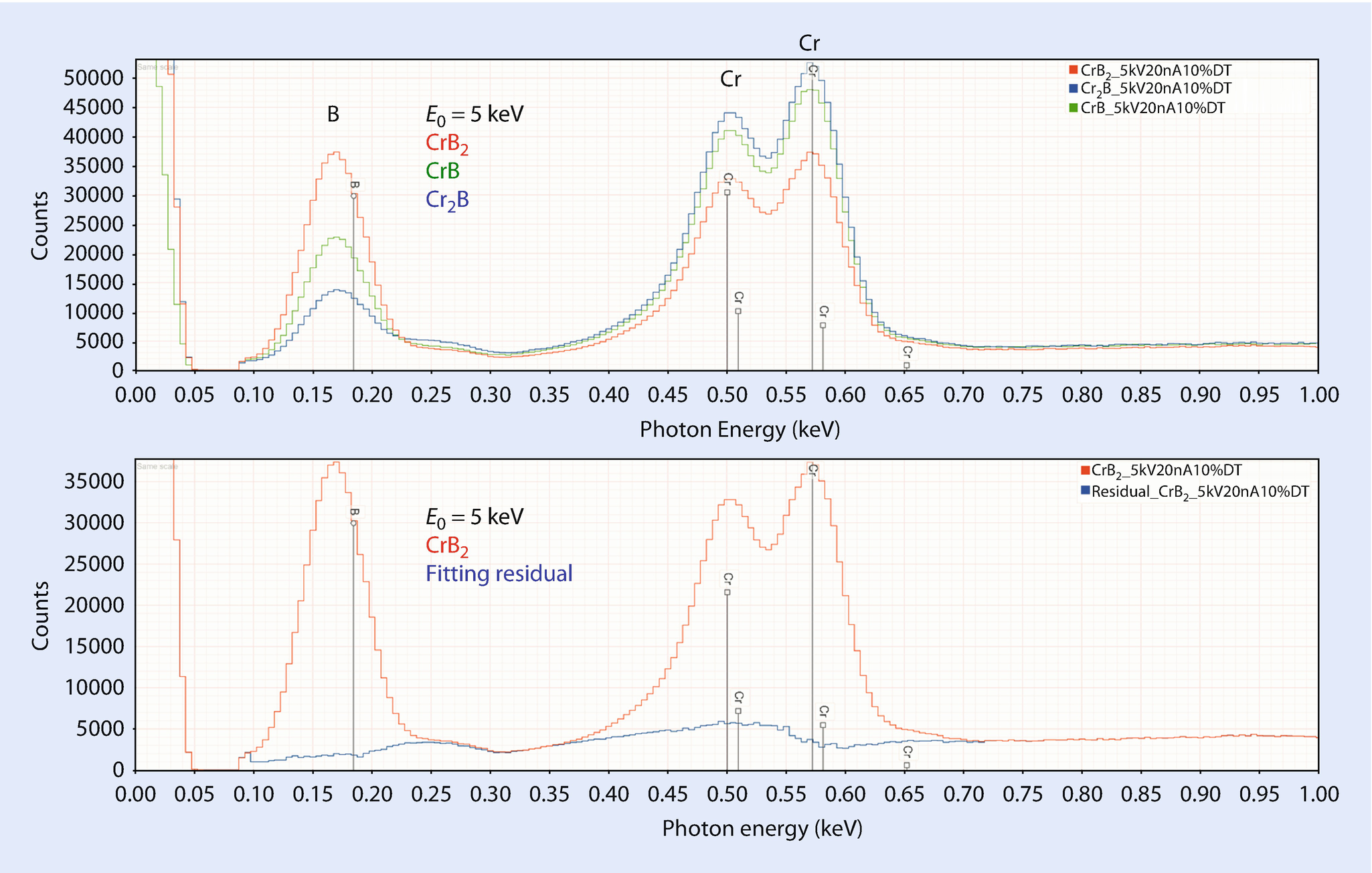
EDS spectra of chromium borides: CrB2, CrB and Cr2B (upper) and residual after peak fitting for B and Cr in CrB2 (lower); E 0 = 5 keV
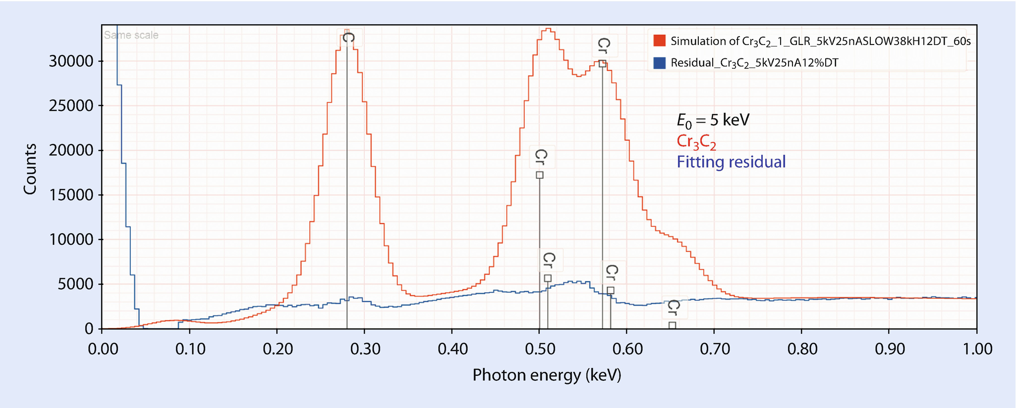
EDS spectrum of chromium carbide, Cr3C2 and residual after peak fitting for C and Cr; E 0 = 5 keV

EDS spectrum of iron nitride, Fe3N and residual after peak fitting for N and Fe; E 0 = 5 keV

EDS spectra of copper oxides, Cu2O and CuO; E 0 = 5 keV
22.3 Challenges and Limitations of Low Beam Energy X-Ray Microanalysis
22.3.1 Reduced Access to Elements
High performance SEMs can routinely operate with the beam energy as low as 500 eV; and with special electron optics and/or stage biasing, the landing kinetic energy of the beam can be reduced to 10 eV. Because the beam penetration depth decreases rapidly as the incident energy is reduced, as shown in ◘ Fig. 22.9, which plots the Kanaya–Okayama range for 0 – 5 keV, low kinetic energy provides extreme sensitivity to the surface of the specimen, which can improve the contrast from surface features of interest. Since the lateral ranges over which the backscattered electron (BSE) and closely related SE2 signals are emitted are also greatly restricted at low beam energies, these signals closely approach the beam footprint of SE1 emission and thus contribute to high spatial resolution imaging rather than degrading resolution as they do at high beam energy. Thus, low beam energy operation has strong advantages for SEM imaging down to beam landing energies of tens of eV.
While low beam energy SEM imaging can exploit the full range of landing kinetic energies to seek to maximize contrast from surface features of interest, the situation for low beam energy X-ray microanalysis is much more constrained. As discussed above, as the beam energy is reduced, the atomic shells that can be ionized become more restricted. A beam energy of 5 keV is the lowest energy that provides access to measureable X-rays for elements of the periodic table from Z = 3 (Li) to Z = 94 (Pu), as shown in ◘ Fig. 22.5. If the beam energy is reduced to E 0 = 2.5 keV, EDS X-ray microanalysis of large portions of the periodic table is no longer possible because no atomic shell with useful X-ray yield can be excited or effectively measured for these elements, creating the situation shown in ◘ Fig. 22.6. Further decreases in the beam energy results in losing access to even more elements, with only about half of the elements measureable at E 0 = 1 keV, and many of those only marginally so.
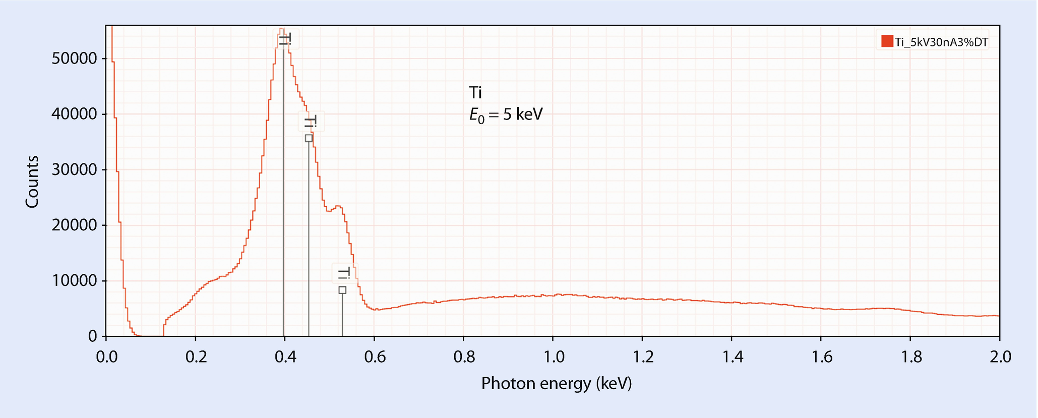
EDS spectrum of titanium; E 0 = 5 keV

EDS spectrum of barium chloride, showing the Ba M-family (upper); EDS spectra of BaCl2, BaF2, and BaCO3 (lower); E 0 = 5 keV

EDS spectrum of YBa2Cu3O7-X, and residual after peak fitting for O K-L2, the Ba M-family and Cu L-family; E 0 = 2.5 keV
Analysis of YBa2Cu3O7-X at E 0 = 2.5 keV
Element | C av mass conc | RDEV % | σ rel, % | C av mass conc | RDEV % | σ rel, % |
|---|---|---|---|---|---|---|
O | 0.1574 (stoich) | −6.4 | 1.1 | 0.1787 (ZnO) | 6.3 | 1.3 |
Cu | 0.2910 | 1.7 | 3.4 | 0.3024 | 5.7 | 1.4 |
Y | 0.1296 | −2.9 | 3.1 | 0.1322 | −0.90 | 2.4 |
Ba | 0.4220 | 2.4 | 3.6 | 0.3867 | −6.2 | 2.3 |
22.3.2 Relative Depth of X-Ray Generation: Susceptibility to Vertical Heterogeneity
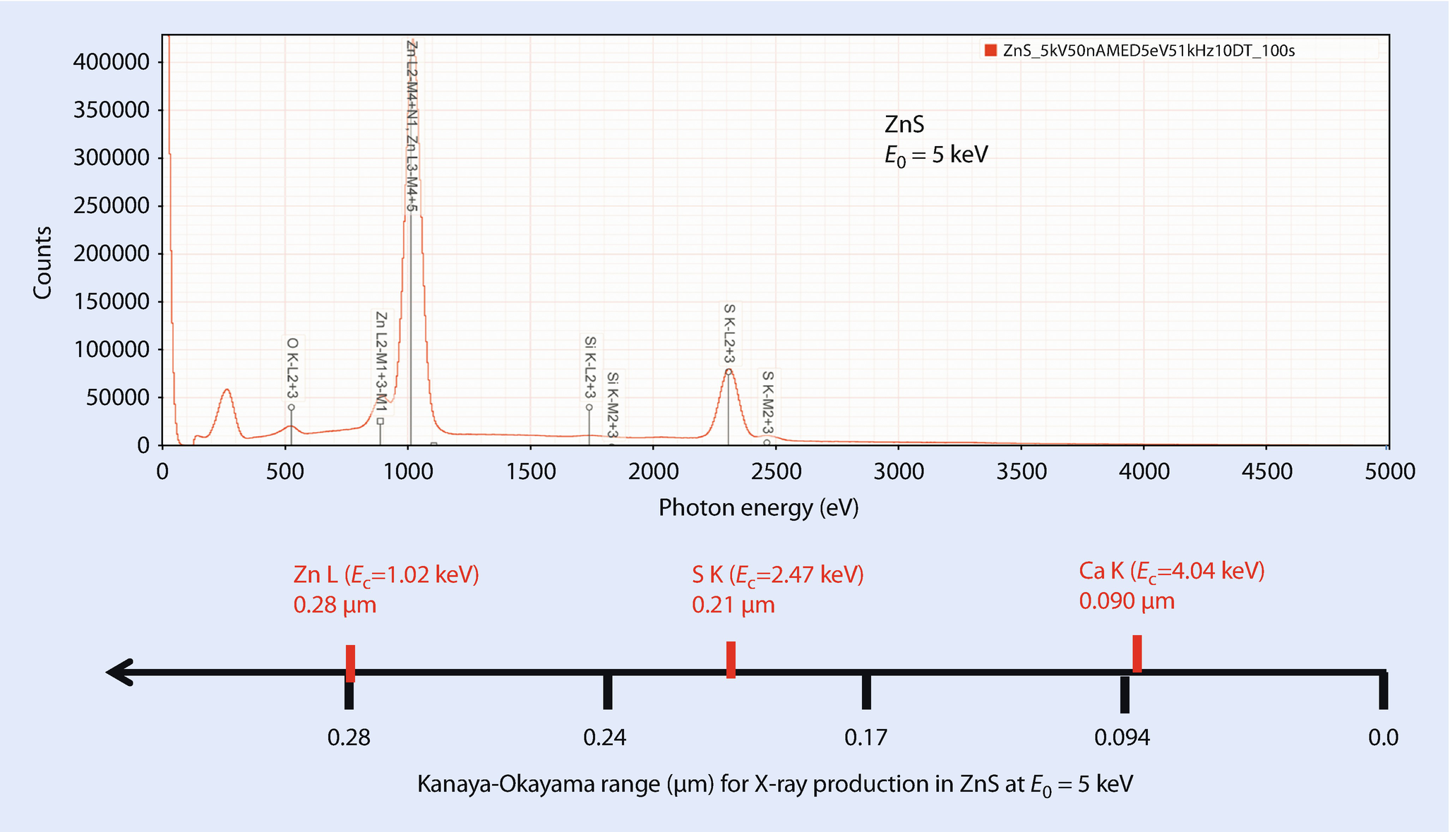
EDS spectrum of ZnS illustrating concept of the energy axis of the spectrum and the corresponding depth of X-ray generation; E 0 = 5 keV
22.3.3 At Low Beam Energy, Almost Everything Is Found To Be Layered
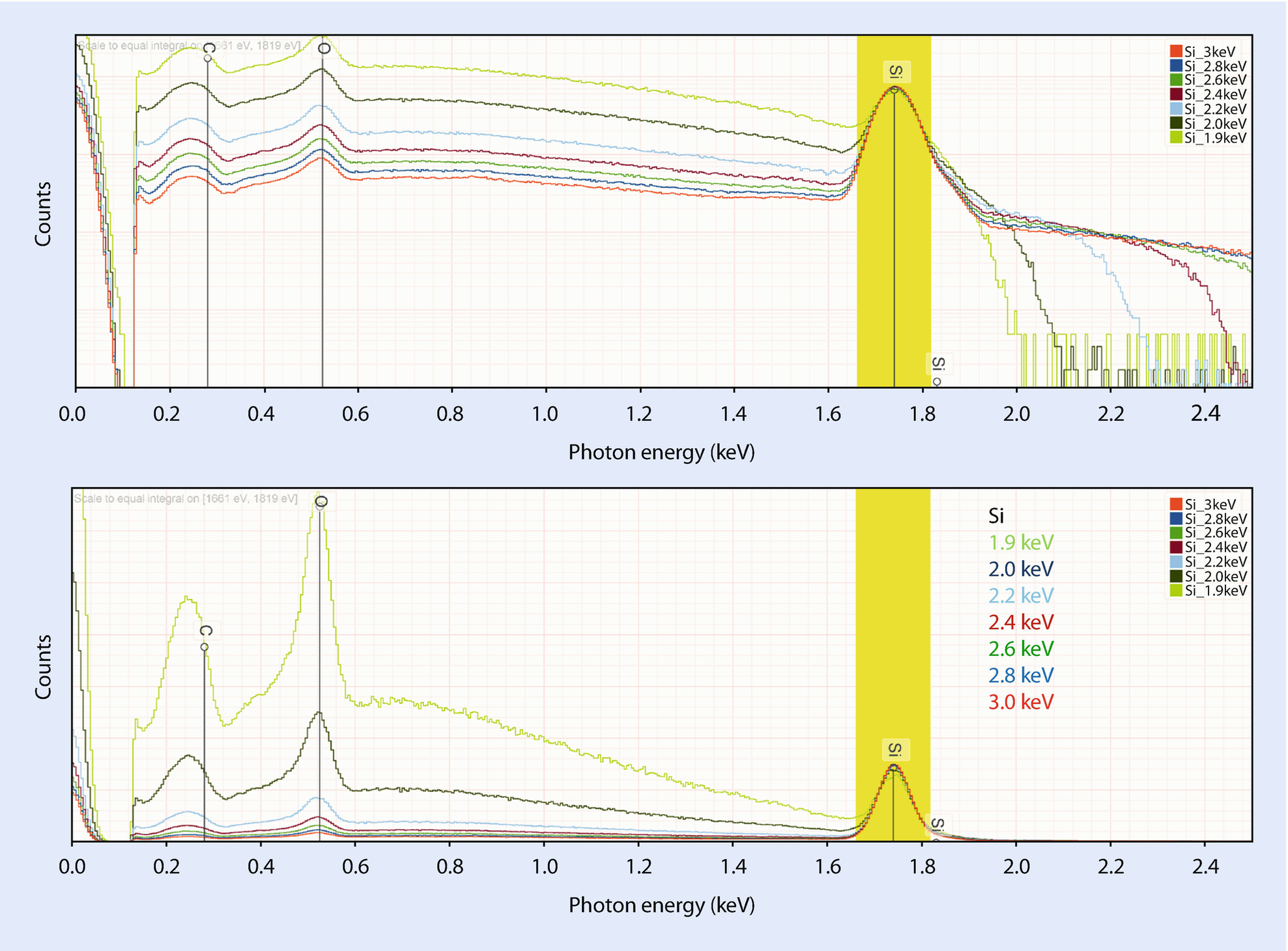
EDS spectra of Si over a range of beam energies, showing increase in the O K-L2 peak relative to Si K-L2; all spectra scaled to Si K-L2
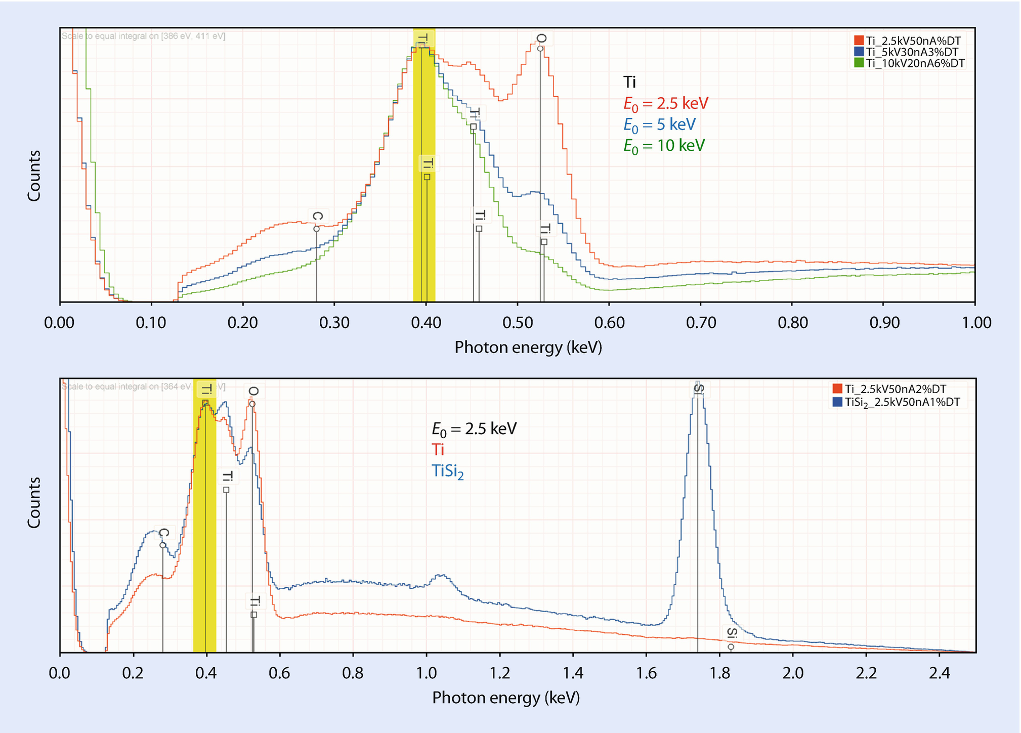
(Upper) EDS spectra of Ti at various beam energies showing increase in the O K-L2 peak relative to Ti L-family peaks; (lower) EDS spectra of Ti and TiSi2 at E 0 = 2.5 keV

EDS Spectra of benitoite (BaTiSi3O9) over arrange of beam energies showing relative increase in the C K-L2 peak as the beam energy decreases

(Upper) EDS spectrum of TiB2 and residual spectrum after fitting for B K-L2 and Ti L-family revealing peaks for C K-L2and O K-L2; (lower) after fitting for C K-L2and O K-L2; E 0 = 2.5 keV
Analysis of TiB2 at E 0 = 2.5 keV
B (atomic concentration) | C (atomic concentration) | O (atomic concentration) | Ti (atomic concentration) | |
|---|---|---|---|---|
Mean (5 analyses) | 0.5110 | 0.0708 | 0.1011 | 0.3171 |
σrel, % | 2.7 | 27 | 11 | 2.7 |
22.3.3.1 Analysis of Surface Contamination

NIST SRM 481 (Au-Ag alloys). Analysis of an old (>30 years) metallographic preparation at E 0 = 5 keV, and the spectrum after repolishing with 0.25 μm diamond abrasive
Analysis of SRM 481 (Au-Ag alloys); 1970s metallographic preparation, original surface; E 0 = 5 keV; standards: S (FeS2); Cl (KCl); Ag, Au
Alloy | Raw analytical total | S (norm mass conc) | σ(%)5 loc | Cl (norm mass conc) | σ(%) 5 loc | Au (norm mass conc) | σ(%)5 loc | RDEV(%) | Ag (norm mass conc) | σ(%) 5 loc | RDEV (%) |
|---|---|---|---|---|---|---|---|---|---|---|---|
20Au–80Ag | 0.9855 | 0.0934 | 4.4 | 0.1061 | 12 | 0.0796 | 12 | −64 | 0.7210 | 0.44 | −7 |
40Au–60Ag | 0.9959 | 0.0311 | 5.7 | 0.0965 | 10 | 0.3440 | 6.1 | −14 | 0.5284 | 2.2 | −12 |
60Au–40Ag | 0.9951 | 0.0094 | 5 | 0.045 | 22 | 0.5754 | 4.7 | −4.2 | 0.3706 | 4.6 | −7.2 |
80Au–20Ag | 1.005 | 0.0051 | 8.3 | 0.0365 | 4.5 | 0.7340 | 0.67 | −8.3 | 0.2244 | 1.6 | +12 |
Analysis of SRM 481 (Au-Ag alloys); surface after first repolishing with 0.25-μm diamond; E 0 = 5 keV; standards: Ag, Au
Alloy | Raw analytical total | Au (norm) | σ(%) 5 loc | RDEV (%) | DTSA-II error budget (%) | Ag (norm) | σ(%) 5 loc | RDEV (%) | DTSA-II error budget (%) |
|---|---|---|---|---|---|---|---|---|---|
20Au–80Ag | 0.9731 | 0.3050 | 7.1 | +36 | 0.34 | 0.6950 | 3.1 | −10.4 | 0.75 |
40Au–60Ag | 0.9920 | 0.4460 | 0.96 | +11.4 | 0.25 | 0.5540 | 0.77 | −7.6 | 1.1 |
60Au–40Ag | 0.9907 | 0.6322 | 1.0 | +5.3 | 0.21 | 0.3678 | 1.8 | −7.9 | 1.5 |
80Au–20Ag | 0.9930 | 0.8264 | 0.24 | 3.2 | 0.17 | 0.1736 | 1.1 | −13 | 2.1 |
Analysis of SRM 481 (Au-Ag alloys); surface after second repolishing with 1- and 0.25-μm diamond; E 0 = 5 keV; standards: Ag, Au
Alloy | Raw analytical total | Au (norm) | σ(%) 5 loc | RDEV (%) | DTSA-II error budget (%) | Ag (norm) | σ(%) 5 loc | RDEV (%) | DTSA-II error budget (%) |
|---|---|---|---|---|---|---|---|---|---|
20Au–80Ag | 1.005 | 0.2398 | 0.87 % | +6.9 % | 0.38 % | 0.7602 | 0.28 % | −2.0 % | 0.64 % |
40Au–60Ag | 0.9983 | 0.4045 | 0.23 | +1.1 | 0.27 | 0.5955 | 0.16 | −0.64 | 0.98 |
60Au–40Ag | 0.9897 | 0.6084 | 0.13 | +1.3 | 0.21 | 0.3916 | 0.21 | −1.9 | 1.4 |
80Au–20Ag | 0.9998 | 0.8055 | 0.26 | +0.62 | 0.19 | 0.1945 | 1.1 | −2.5 | 1.9 |
20Au–80Ag | 1.005 | 0.2398 | 0.87 | +6.9 | 0.38 | 0.7602 | 0.28 | −2.0 | 0.64 |
Analysis of SRM 481 (Au-Ag alloys); surface after third repolishing with 1- and 0.25-μm diamond; E 0 = 5 keV; standards: Ag, Au
Alloy | Raw analytical total | Au (norm) | σ(%) 5 loc | RDEV (%) | DTSA-II error budget (%) | Ag (norm) | σ(%) 5 loc | RDEV (%) | DTSA-II error budget (%) |
|---|---|---|---|---|---|---|---|---|---|
20Au–80Ag | 1.017 | 0.2251 | 0.13 | −0.11 | 0.39 | 0.7749 | 0.13 | +0.35 | 0.61 |
40Au–60Ag | 0.9988 | 0.3909 | 0.25 | −2.3 | 0.28 | 0.6091 | 0.16 | +1.6 | 0.93 |
60Au–40Ag | 0.9931 | 0.5931 | 0.12 | −1.2 | 0.22 | 0.4069 | 0.18 | +1.9 | 1.4 |
80Au–20Ag | 0.9957 | 0.7979 | 0.17 | −0.32 | 0.18 | 0.2021 | 0.68 | +1.2 | 1.9 |

Open Access This chapter is licensed under the terms of the Creative Commons Attribution-NonCommercial 2.5 International License (http://creativecommons.org/licenses/by-nc/2.5/), which permits any noncommercial use, sharing, adaptation, distribution and reproduction in any medium or format, as long as you give appropriate credit to the original author(s) and the source, provide a link to the Creative Commons license and indicate if changes were made.
The images or other third party material in this chapter are included in the chapter's Creative Commons license, unless indicated otherwise in a credit line to the material. If material is not included in the chapter's Creative Commons license and your intended use is not permitted by statutory regulation or exceeds the permitted use, you will need to obtain permission directly from the copyright holder.