© Springer Science+Business Media LLC 2018
Joseph I. Goldstein, Dale E. Newbury, Joseph R. Michael, Nicholas W.M. Ritchie, John Henry J. Scott and David C. JoyScanning Electron Microscopy and X-Ray Microanalysishttps://doi.org/10.1007/978-1-4939-6676-9_27

27. X-Ray Microanalysis Case Studies

Joseph I. Goldstein1 , Dale E. Newbury2, Joseph R. Michael3, Nicholas W. M. Ritchie2, John Henry J. Scott2 and David C. Joy4
(1)
University of Massachusetts, Amherst, Massachusetts, USA
(2)
National Institute of Standards and Technology, Gaithersburg, Maryland, USA
(3)
Sandia National Laboratories, Albuquerque, New Mexico, USA
(4)
University of Tennessee, Knoxville, Tennessee, USA
 

27.1 Case Study: Characterization of a Hard-Facing Alloy Bearing Surface

Background: As part of a study into the in-service failure of the bearing surface of a large water pump, characterization was requested of the hard-facing alloy, which was observed to have separated from the stainless steel substrate, causing the failure.

This problem illustrates the critical importance of careful specimen preparation of a macroscopic object with centimeter dimensions to locate regions of microscopic interest with micrometer dimensions. Metallographic preparation produced a polished cross section of an intact portion of the hard-facing alloy layer as deposited onto the stainless steel base, as shown in ◘ Fig. 27.1. SEM-EDS analysis with DTSA-II gave the results shown in ◘ Fig. 27.2 for the stainless steel base and at one location in the hard-facing alloy. EDS elemental mapping produced the images shown in ◘ Fig. 27.3. The SEM-BSE image (◘ Fig. 27.1) revealed the presence of numerous voids that were predominantly located (white arrows) at the interface between the hard-facing alloy and the stainless steel substrate, with a smaller population of voids located within the hard-facing alloy (yellow arrows). The elemental maps (◘ Fig. 27.3) revealed that the hard-facing alloy layer had a very complex microstructure with distinct heterogeneity. The voids were found to be closely associated with regions with that had elevated Cr, both near the hard-facing alloy-stainless steel interface and within the hard-facing alloy. These voids severely compromised the performance of the bearing surface.
../images/271173_4_En_27_Chapter/271173_4_En_27_Fig1_HTML.jpg
Fig. 27.1

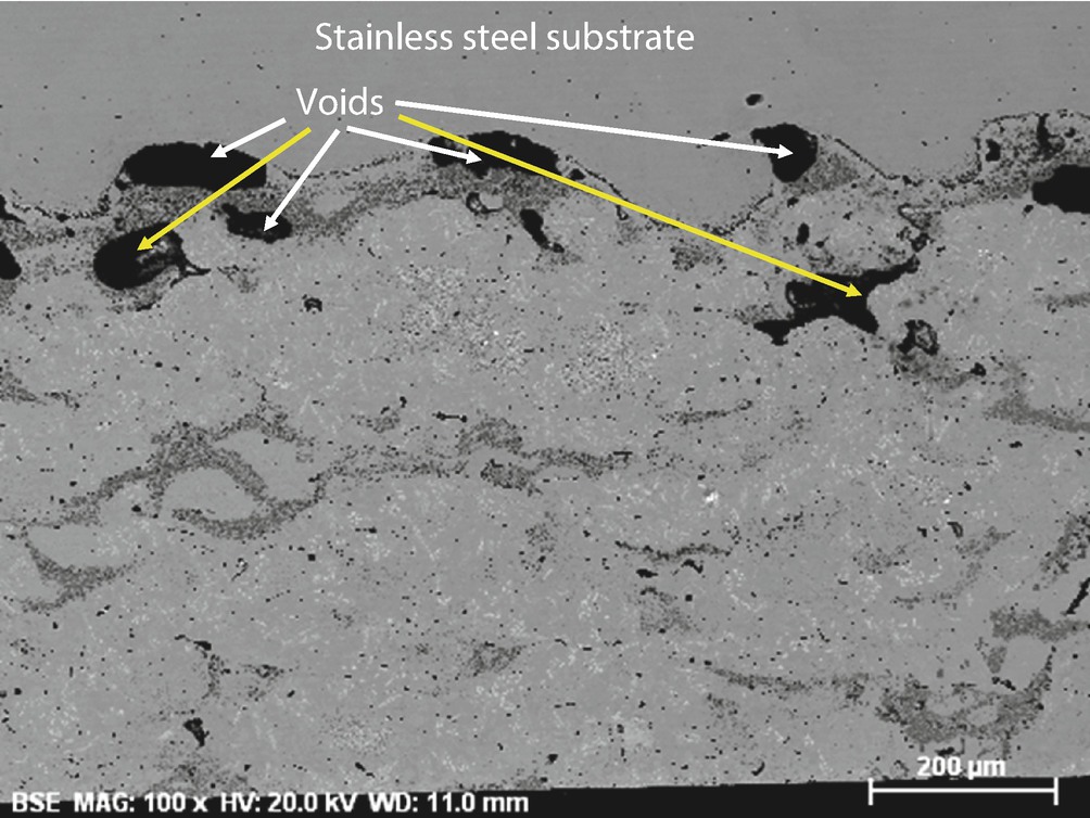
SEM-BSE image of the cross-section of a hard-facing alloy deposited on a stainless steel substrate. Note the voids at the interface between the hard-facing alloy and the stainless substrate (white arrows), as well as a smaller population of voids entirely within the hard-facing alloy (green arrows)

../images/271173_4_En_27_Chapter/271173_4_En_27_Fig2_HTML.jpg
Fig. 27.2

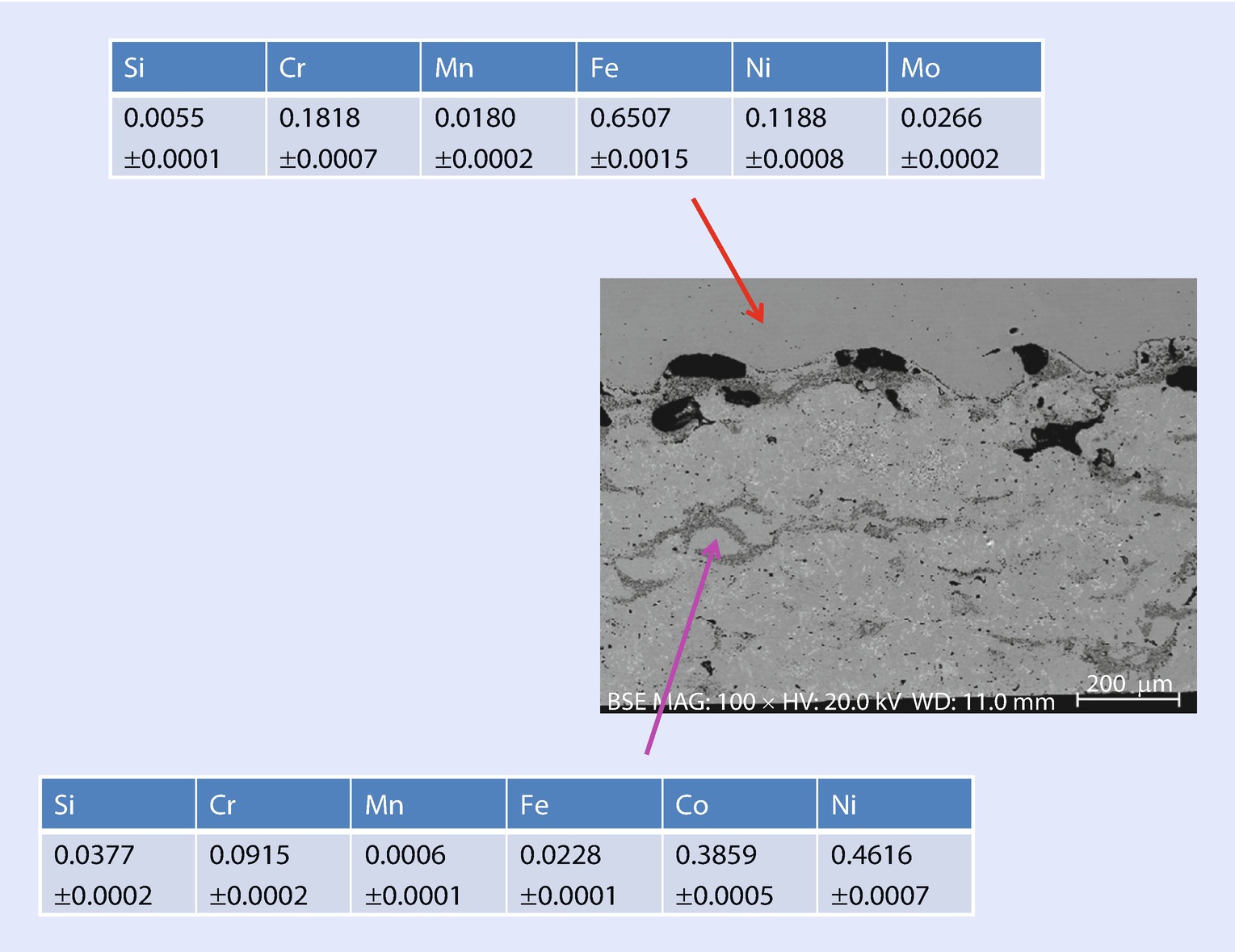
SEM-BSE image showing locations of SEM-EDS analyses with NIST DTSA-II

../images/271173_4_En_27_Chapter/271173_4_En_27_Fig3_HTML.png
Fig. 27.3

Elemental mapping, with color overlay: Ni = red; Cr = green; Co = blue

Complex fine-grained regions were also observed within the hard-facing alloy, as shown in the elemental maps in ◘ Fig. 27.4 and the SEM-BSE image in ◘ Fig. 27.5, which shows strong atomic number contrast. SEM-EDS analysis with DTSA-II gave the results presented in ◘ Fig. 27.5, which confirm the gray scale sequence as a function of composition, with the sharp rise in W (see table in ◘ Fig. 27.5) dominating backscattering.
../images/271173_4_En_27_Chapter/271173_4_En_27_Fig4_HTML.png
Fig. 27.4

Elemental mapping of an area of fine-scale grains

../images/271173_4_En_27_Chapter/271173_4_En_27_Fig5_HTML.jpg
Fig. 27.5

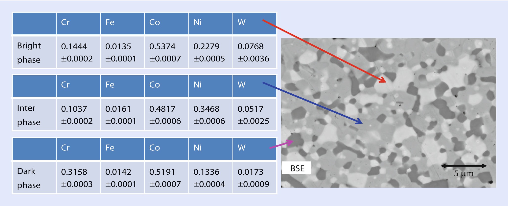
SEM-BSE image and DTSA-II analyses of selected grains in the fine-scale region

The information provided by SEM-EDS enabled metallurgists to modify the hard-facing alloy composition and deposition conditions to eliminate the void formation during deposition, producing satisfactory service behavior.

27.2 Case Study: Aluminum Wire Failures in Residential Wiring

Background: In the early 1970s, aluminum wire was used extensively as a substitute for more expensive copper wire in residential and commercial wiring, specifically for 110 V electrical outlets that used steel screw compressive clamping of the wire against a brass or steel plate. The aluminum wire–steel screw junctions were observed to fail catastrophically through a process of overheating, leading in extreme cases to initiation of structural fires (Meese and Beausoliel 1977; Rabinow 1978). ◘ Figure 27.6 shows an example of the damage to the wire-screw junction and the surrounding plastic housing and wire insulation caused during an overheating event observed in a laboratory test. This failure was a puzzling occurrence, since aluminum is an excellent electrical conductor and was long used successfully in high voltage electrical transmission lines. Moreover, the vast majority of Al wire–screw connections provided proper service without overheating. However, those connections that did fail in service often produced such catastrophic effects that the critical evidence of the initiation of the failure was destroyed. Capturing an event like that shown in ◘ Fig. 27.6 required intensive laboratory studies in which thousands of junction boxes were tested and continuously monitored with thermal sensors until a failure initiated, which was then automatically interrupted to prevent complete destruction of the evidence.
../images/271173_4_En_27_Chapter/271173_4_En_27_Fig6_HTML.png
Fig. 27.6

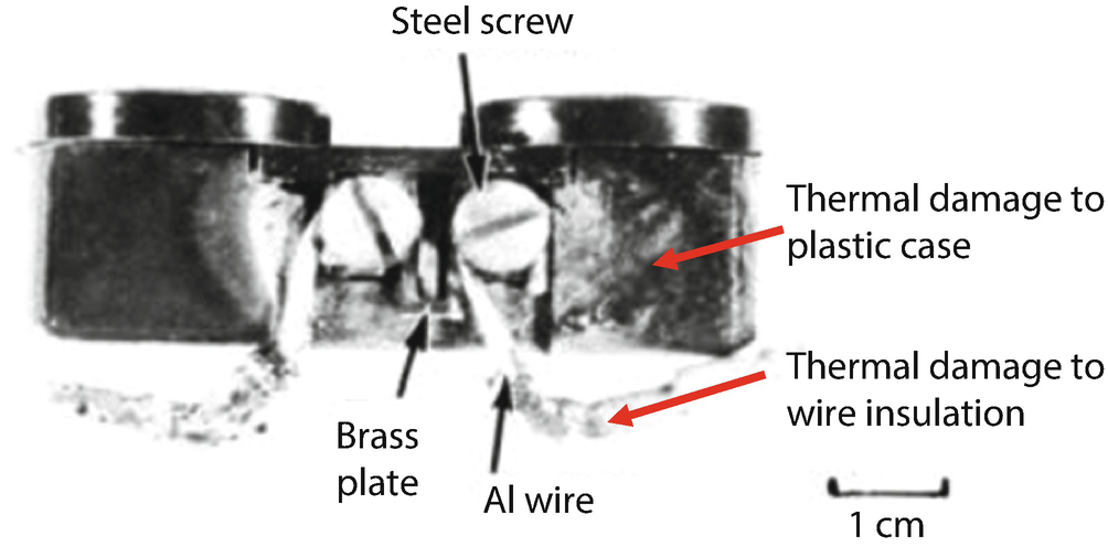
Residential electrical outlet wired with aluminum. The laboratory test was interrupted after the thermal event initiated and was automatically detected, but significant thermal damage to the plastic casing and wire insulation still occurred

This problem illustrates the “macro to micro” sampling problem. The failure mechanism was eventually discovered by SEM/EDS characterization to have a microscopic point of origin, but this microscopic failure origin with micrometer dimensions was hidden within a complex macroscopic structure with centimeter dimensions. Solving the problem required a careful sample preparation strategy to locate the unknown feature(s) of interest. The metallographer mounted the entire Al-wire/steel screw/brass plate assembly in epoxy, as shown in ◘ Fig. 27.7, and sequentially ground and polished through the structure until an anomalous region was revealed (◘ Fig. 27.8). As shown with SEM/BSE imaging and elemental mapping in ◘ Fig. 27.9, in this anomalous region the aluminum and iron had reacted to form two distinct Al-Fe zones (Newbury and Greenwald 1980; Newbury 1982). Fixed beam quantitative X-ray microanalysis with NIST DTSA II and pure element standards (analyses performed during a revisiting of the 1980 specimens) produced the results shown in ◘ Fig. 27.10, where zone 1 is found to correspond closely to the intermetallic compound FeAl3, while zone 2 corresponds to Fe2Al5. The presence of these intermetallic compounds is significant because of their resistivity. FeAl3 and Fe2Al5 have electrical resistivities of approximately 1 μΩ–m, similar to that of the alloy nichrome (1.1 μΩ–m), which is used for resistive heating elements and which is a factor of 38 higher than pure Al and 10.3 higher than pure Fe. The formation of these intermetallic compounds at the screw-wire contact was initiated when electrical arcing occurred because the connection became mechanically loose due to creep of the Al wire and the poor compliance (springiness) of the wire–screw clamp. Once the local formation of the intermetallic compounds had been initiated by arcing followed by local welding of the Al wire and the steel screw, the increased resistivity caused localized resistive heating that stimulated the interdiffusion of Al and Fe, leading to the further intermetallic compound growth in a runaway positive feedback. Eventually this intermetallic compound zone expanded to dimensions of several hundred micrometers, as seen in ◘ Fig. 27.7, creating a resistive heating element that caused the damage seen in ◘ Fig. 27.6. (Note that the practical solution to this problem was to modify the wire connections to provide much greater springiness to eliminate the opening of gaps that allowed arcing to occur.)
../images/271173_4_En_27_Chapter/271173_4_En_27_Fig7_HTML.jpg
Fig. 27.7

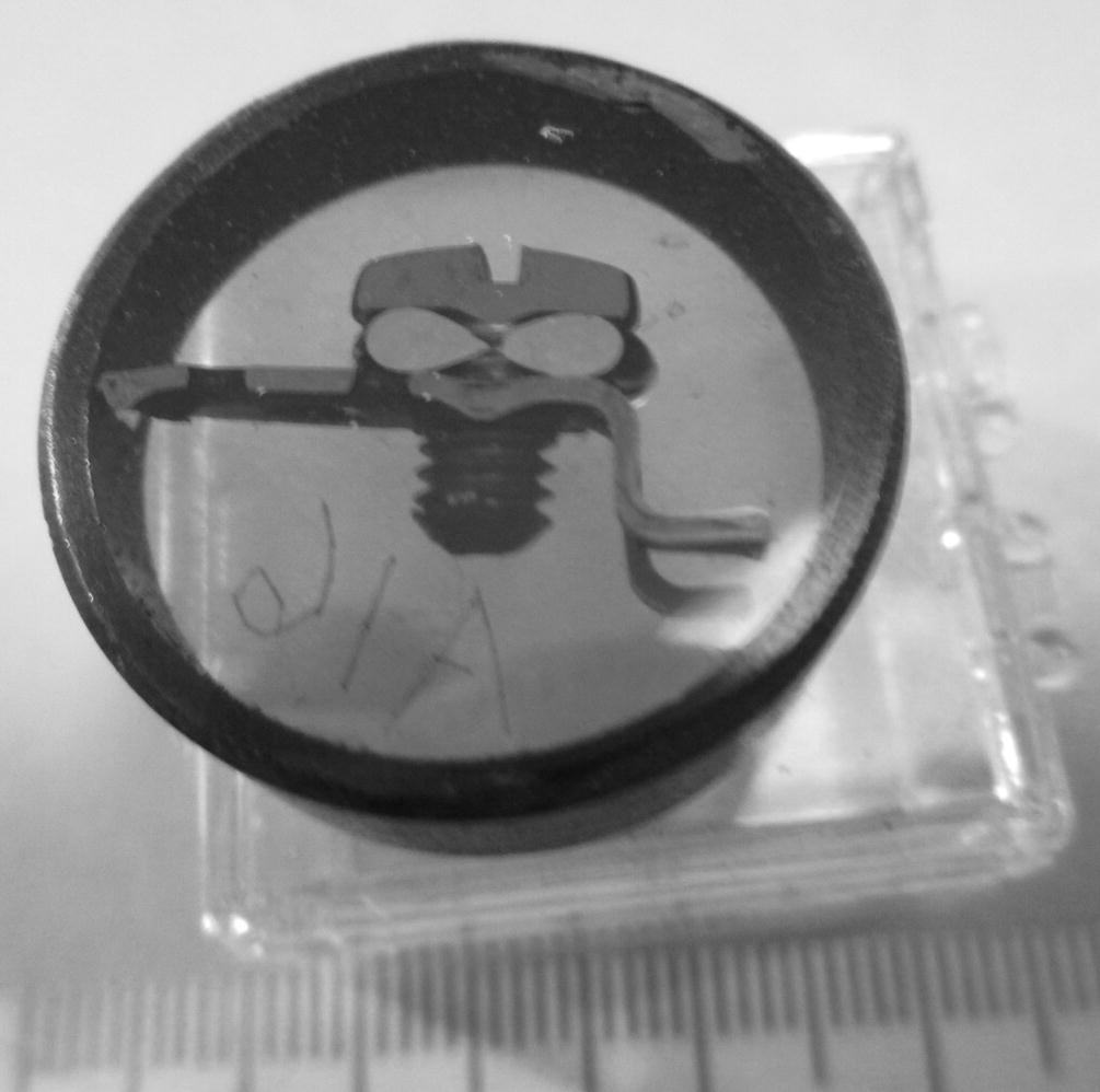
Metallographic mount (2.5-cm diameter) showing the cross section of the steel screw, aluminum wire, and brass plate

../images/271173_4_En_27_Chapter/271173_4_En_27_Fig8_HTML.jpg
Fig. 27.8

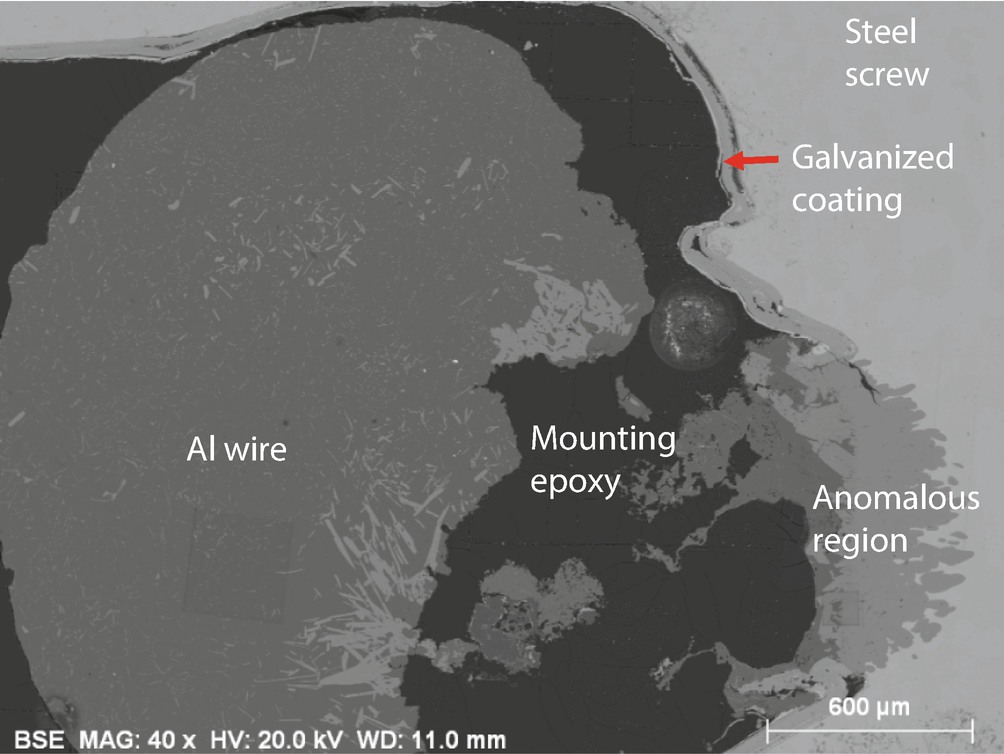
SEM-BSE image of an anomalous zone of contact between the Al wire and the Fe screw

../images/271173_4_En_27_Chapter/271173_4_En_27_Fig9_HTML.jpg
Fig. 27.9

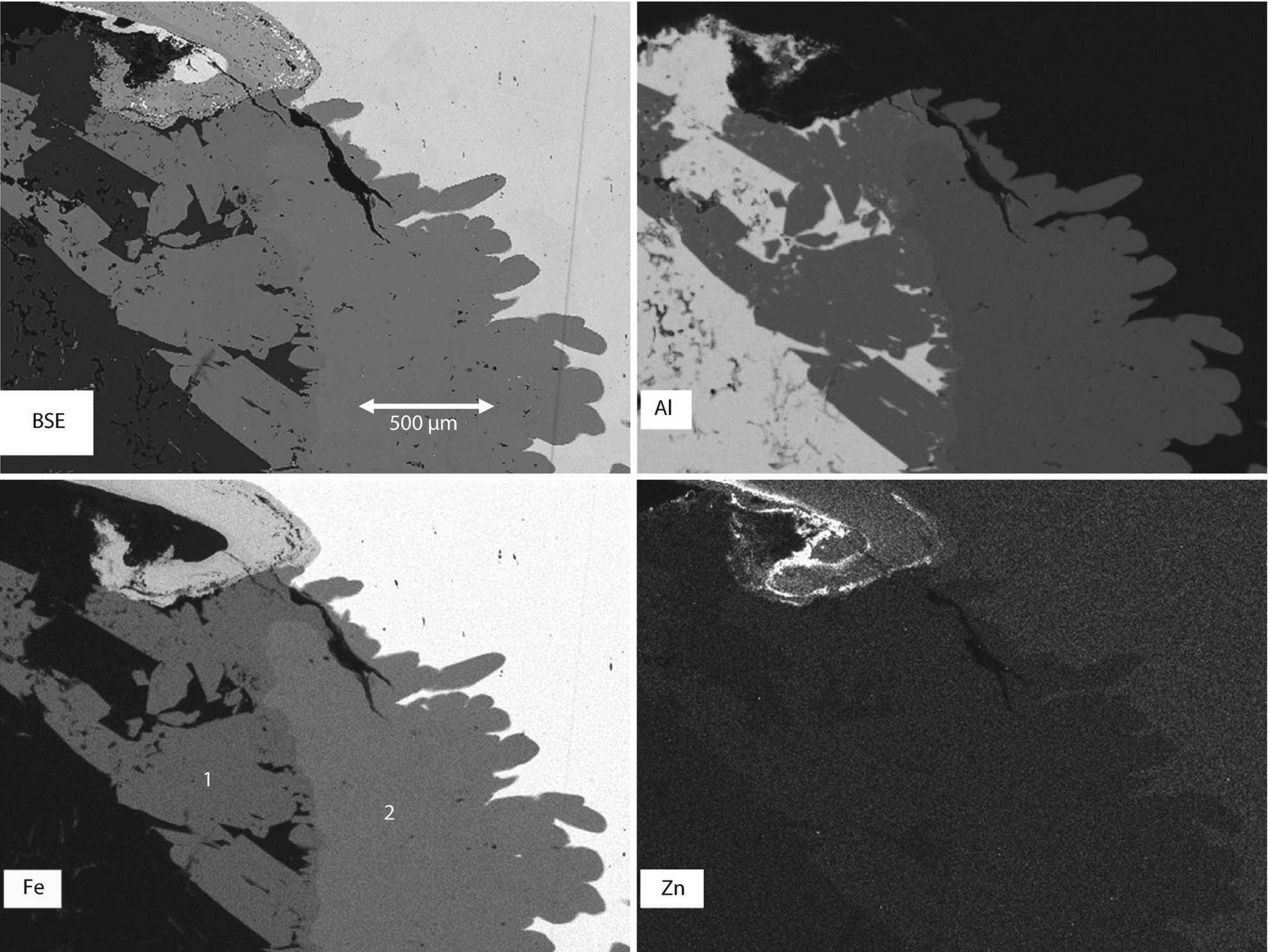
SEM-BSE image and elemental maps for Al, Fe, and Zn of the anomalous contact zone

../images/271173_4_En_27_Chapter/271173_4_En_27_Fig10_HTML.png
Fig. 27.10

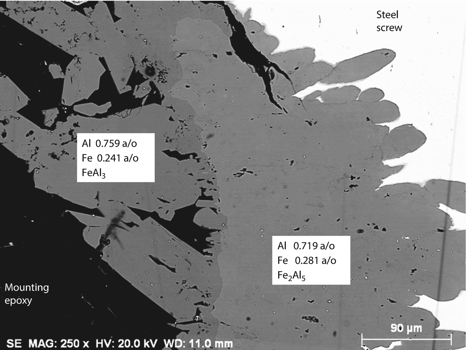
SEM-BSE image of the anomalous zone of contact with quantitative X-ray microanalysis results from fixed-beam analysis in the two distinct Al-Fe regions (note the contrast in the BSE image)

27.3 Case Study: Characterizing the Microstructure of a Manganese Nodule

“Manganese nodules” are rock concretions that form on the deep sea floor through the action of microorganisms that precipitate solid chemical forms from metals dissolved in the water, often in close association with hydrothermal vents.
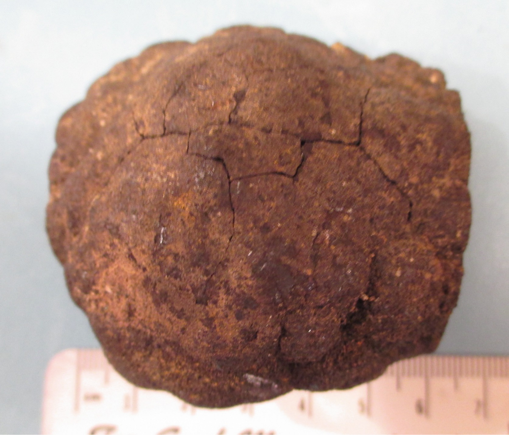
The elemental composition of a polished cross section of a manganese nodule, shown in ◘ Fig. 27.11, was examined by SEM/BSE and by SEM/EDS X-ray spectrum imaging elemental mapping. The SEM/BSE image in ◘ Fig. 27.12 reveals a complex layered microstructure that suggests non-uniform deposition of the precipitated minerals over time. This non-uniform deposition is confirmed by the elemental maps for O, Mn, and Ni and color overlay shown in ◘ Fig. 27.13 and for the Mn, Fe, and Ni maps shown in ◘ Fig. 27.14. Note the oxygen-rich areas (green) in ◘ Fig. 27.13. These regions correspond to silica and aluminosilicate grains within the manganese nodule, as revealed in ◘ Fig. 27.15. The composition measured with a fixed beam placed at the center of the field of view is listed in ◘ Table 27.1, showing the high abundance of Mn as a major constituent and the presence of other transition elements (e.g., Fe, Ni, and Cu) as minor constituents. ◘ Figure 27.16 shows the results of quantitative processing of the XSI with the k-ratio/matrix correction protocol using DTSA-II. The resulting concentration maps have been encoded with the logarithmic three- band color scheme shown in ◘ Fig. 27.16, enabling quantitative comparison of the constituents, using NIST Lispix.
../images/271173_4_En_27_Chapter/271173_4_En_27_Fig11_HTML.png
Fig. 27.11

Manganese nodule

../images/271173_4_En_27_Chapter/271173_4_En_27_Fig12_HTML.png
Fig. 27.12

SEM/BSE image of a polished cross section; note the cracks

../images/271173_4_En_27_Chapter/271173_4_En_27_Fig13_HTML.png
Fig. 27.13

SEM/EDS X-ray spectrum imaging elemental maps for Mn, O, and Ni and color overlay (Mn = red; O = green; Ni = blue). Note cracks are observed in the O map but are much less visible in Mn and Ni

../images/271173_4_En_27_Chapter/271173_4_En_27_Fig14_HTML.png
Fig. 27.14

SEM/EDS X-ray spectrum imaging elemental maps for Mn, Fe, and Ni and color overlay (Mn = red; Fe = green; Ni = blue)

../images/271173_4_En_27_Chapter/271173_4_En_27_Fig15_HTML.png
Fig. 27.15

SEM/EDS X-ray spectrum imaging elemental maps for Mn, Si, and Al and color overlay (Mn = red; Si = green; Al = blue)

Table 27.1

Fixed-beam analysis at the center of ◘ Fig. 27.12; NIST DTSA II analysis with pure element and microanalysis glass standards

O

Na

Mg

Al

Si

K

Ca

Ti

Mn

Fe

Ni

Cu

0.2742 ± 0.0003

0.0420 ± 0.0005

0.0196 ± 0.0002

0.0210 ± 0.0001

0.0458 ± 0.0002

0.0100 ± 0.0000

0.0267 ± 0.0001

0.0031 ± 0.0000

0.4412 ± 0.0003

0.0834 ± 0.0002

0.0196 ± 0.0001

0.0134 ± 0.0002

../images/271173_4_En_27_Chapter/271173_4_En_27_Fig16_HTML.jpg
Fig. 27.16

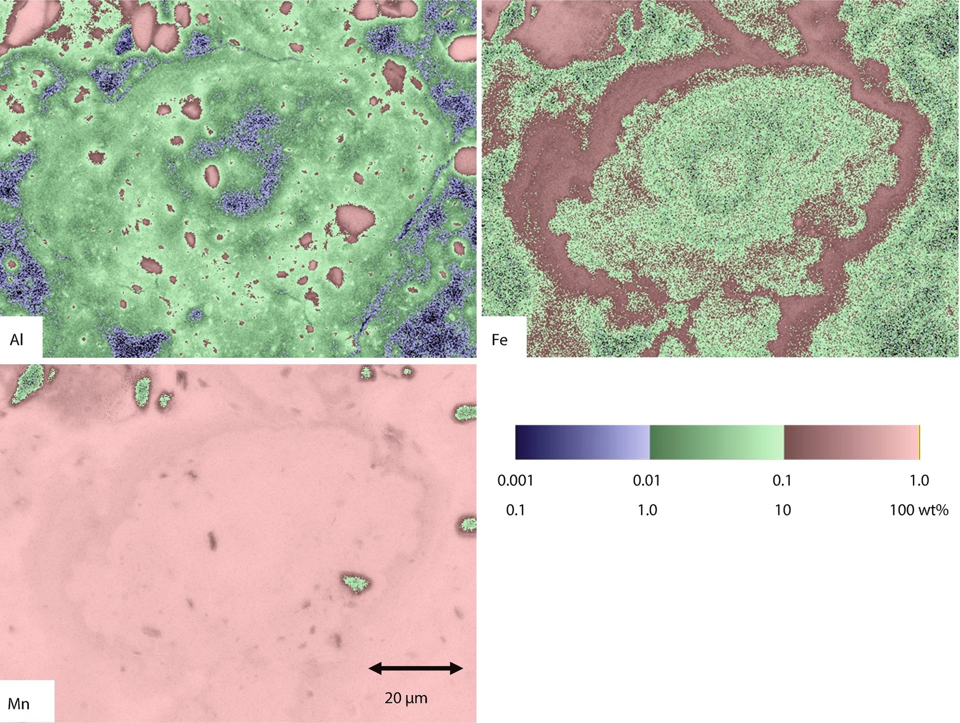
SEM/EDS X-ray spectrum imaging maps after quantitative analysis with DTSA-II presented with logarithmic three-band encoding for Al, Fe, and Mn. Note Fe-enrichment band

Note that some features in the elemental maps are a result of artifacts. Thus, the cracks noted in the SEM/BSE of ◘ Fig. 27.11 are also seen in the O elemental map, but not in the Mn or Ni maps. The origin of this artifact is the difference in the photon energies of these elements. The O K-shell X-ray at an energy of 0.523 keV suffers strong absorption when the electron beam is located in the crack, so that the intensity is greatly reduced, producing an accurate representation of the crack. The MnK-L2,3 (5.898 keV) and NiK-L2,3 (7.477 keV) photons have higher energy and suffer much less absorption, so that most of those photons generated when the beam is in the crack still escape despite having to pass through more material to reach the EDS, greatly reducing the contrast of the cracks relative to the surrounding matrix.

Creative Commons

Open Access This chapter is licensed under the terms of the Creative Commons Attribution-NonCommercial 2.5 International License (http://creativecommons.org/licenses/by-nc/2.5/), which permits any noncommercial use, sharing, adaptation, distribution and reproduction in any medium or format, as long as you give appropriate credit to the original author(s) and the source, provide a link to the Creative Commons license and indicate if changes were made.

The images or other third party material in this chapter are included in the chapter's Creative Commons license, unless indicated otherwise in a credit line to the material. If material is not included in the chapter's Creative Commons license and your intended use is not permitted by statutory regulation or exceeds the permitted use, you will need to obtain permission directly from the copyright holder.