© Springer Science+Business Media LLC 2018
Joseph I. Goldstein, Dale E. Newbury, Joseph R. Michael, Nicholas W.M. Ritchie, John Henry J. Scott and David C. JoyScanning Electron Microscopy and X-Ray Microanalysishttps://doi.org/10.1007/978-1-4939-6676-9_28

28. Cathodoluminescence

Joseph I. Goldstein1 , Dale E. Newbury2, Joseph R. Michael3, Nicholas W. M. Ritchie2, John Henry J. Scott2 and David C. Joy4
(1)
University of Massachusetts, Amherst, Massachusetts, USA
(2)
National Institute of Standards and Technology, Gaithersburg, Maryland, USA
(3)
Sandia National Laboratories, Albuquerque, New Mexico, USA
(4)
University of Tennessee, Knoxville, Tennessee, USA
 

28.1 Origin

Cathodoluminescence (CL) is the emission of low energy photons in the range from approximately 1 eV to 5 eV (infrared, visible, and ultraviolet light) as a result of inelastic scattering of the high energy beam electrons (◘ Fig. 28.1). Materials that can emit such photons are insulators or semiconductors which have an electronic structure with a filled valence band of allowed energy states that is separated by a gap of disallowed energy states from the empty conduction band, as shown schematically in ◘ Fig. 28.2a. Inelastic scattering of the beam electron can transfer energy to a weakly bound valence electron promoting it to the empty conduction band, leaving a positively charged “hole” in the conduction band. When a free electron and a positive hole are attracted and recombine, the energy difference is expressed as a photon, as illustrated in ◘ Fig. 28.2b. Because the possible energy transitions and the resulting photon emission are defined by the intrinsic properties of a high purity material, such as the band-gap energy but also including energy levels that result from physical defects such as lattice vacancies, rather than by the influence of impurity atoms, this type of CL is referred to as “intrinsic CL emission.” Since the valence electron promoted to the conduction band can receive a range of possible kinetic energies depending on the details of the initial scattering, the photons emitted during free electron–hole recombination can have a range of energies, resulting in broad band CL photon emission. Because of the great mismatch in the velocity of the high energy (keV) beam electron and the low energy (eV) valence electron, this is not an efficient process and in general CL emission is very weak. The ionization cross section is maximized for electrons with three to five times the binding energy of the valence electrons, so that most efficient energy transfer to initiate CL emission occurs from the more energetic slow SE (>10 eV) and the fast SE (hundreds of eV) also created by inelastic scattering of the primary electron.
../images/271173_4_En_28_Chapter/271173_4_En_28_Fig1_HTML.jpg
Fig. 28.1

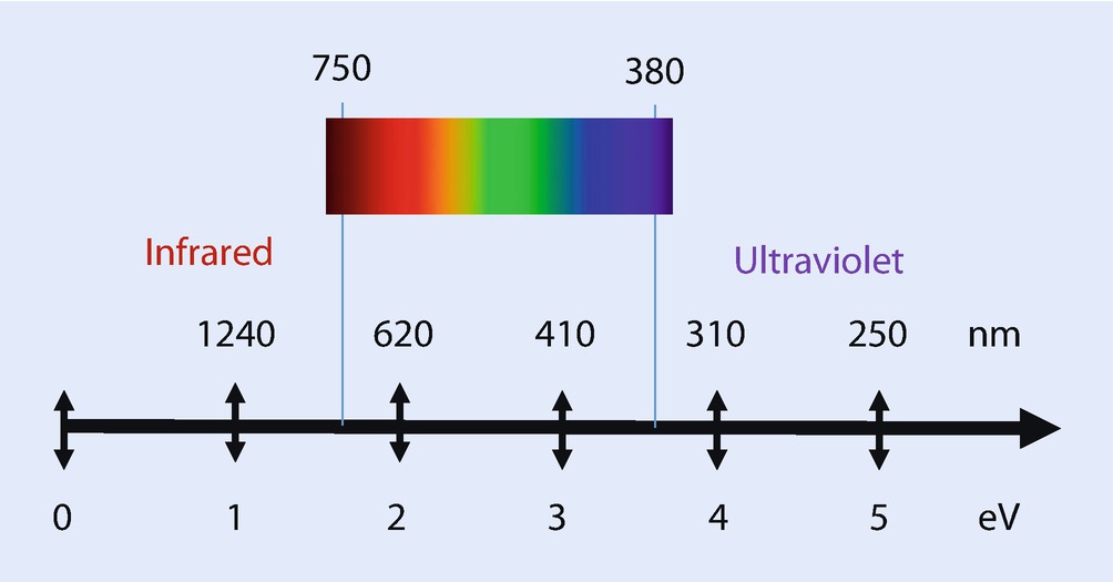
Range of photon energies and wavelengths for cathodoluminescence

../images/271173_4_En_28_Chapter/271173_4_En_28_Fig2_HTML.png
Fig. 28.2

a Origin of intrinsic CL: the material’s electron energy states fill the valence band which is separated by a band-gap of several eV from an empty conduction band. Inelastic scattering of the beam electron promotes a valence band electron to the conduction band, leaving a positively charged hole in the valence band. b Origin of intrinsic CL: The free electron and hole are mutually attracted and recombine, with the energy released as an electromagnetic photon with a minimum energy equal to the band-gap energy

In more complex materials that are modified by impurities, the presence of impurity atoms in the host crystal lattice can create sharply defined energy levels within the band gap to which valence electrons can be scattered, as illustrated in ◘ Fig. 28.3. The subsequent electron–hole transitions that involve these well-defined energy states create a photon or series of photons with a sharply defined energy or series of energies (“extrinsic CL emission”). This sharp line spectrum may be superimposed on a broad range intrinsic spectrum which can still occur.
../images/271173_4_En_28_Chapter/271173_4_En_28_Fig3_HTML.png
Fig. 28.3

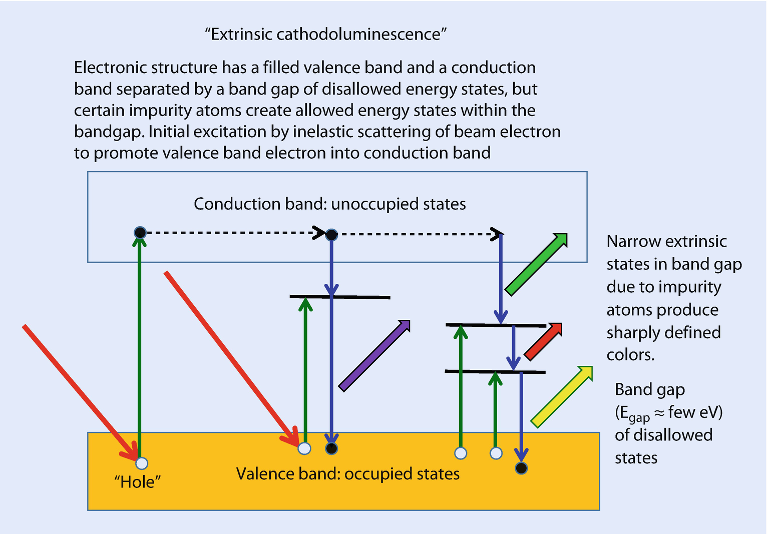
Origin of extrinsic CL: the presence of impurity atoms in the host lattice creates narrow energy levels within the band-gap. Inelastic scattering of the beam electron can promote valence band electrons to the conduction band as well as to the impurity levels in the band-gap. Electron transitions can occur between the various energy levels, creating both broadband CL emission and sharply defined CL emission

28.2 Measuring Cathodoluminescence

Some materials such as the mineral benitoite and the compound ZnS produce such strong CL that the emitted light can be readily observed by the unaided eye, as shown in ◘ Figs. 28.4 and 28.5. However, in general the CL phenomenon is weak, requiring the use of an efficient optical collection scheme for successful measurement.
../images/271173_4_En_28_Chapter/271173_4_En_28_Fig4_HTML.jpg
Fig. 28.4

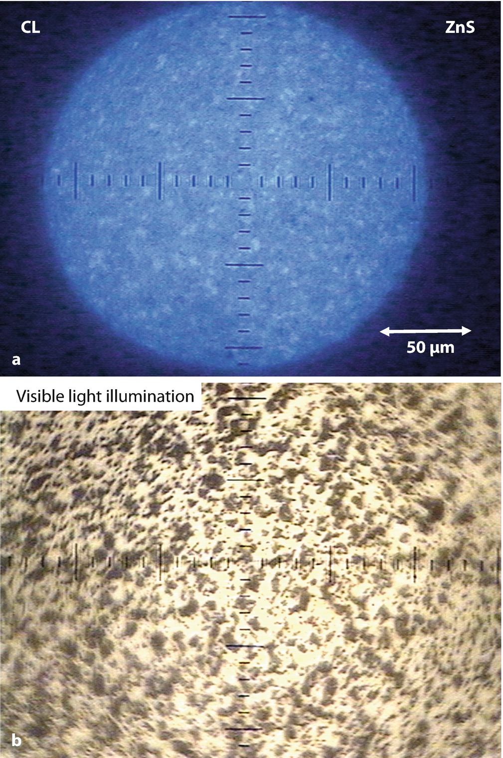
a CL emission from ZnS observed with a defocused 220-μm-diameter beam with 500 nA of beam current at E 0 = 20 keV. b Corresponding white light illumination image with the electron beam blanked into a Faraday cup

../images/271173_4_En_28_Chapter/271173_4_En_28_Fig5_HTML.jpg
Fig. 28.5

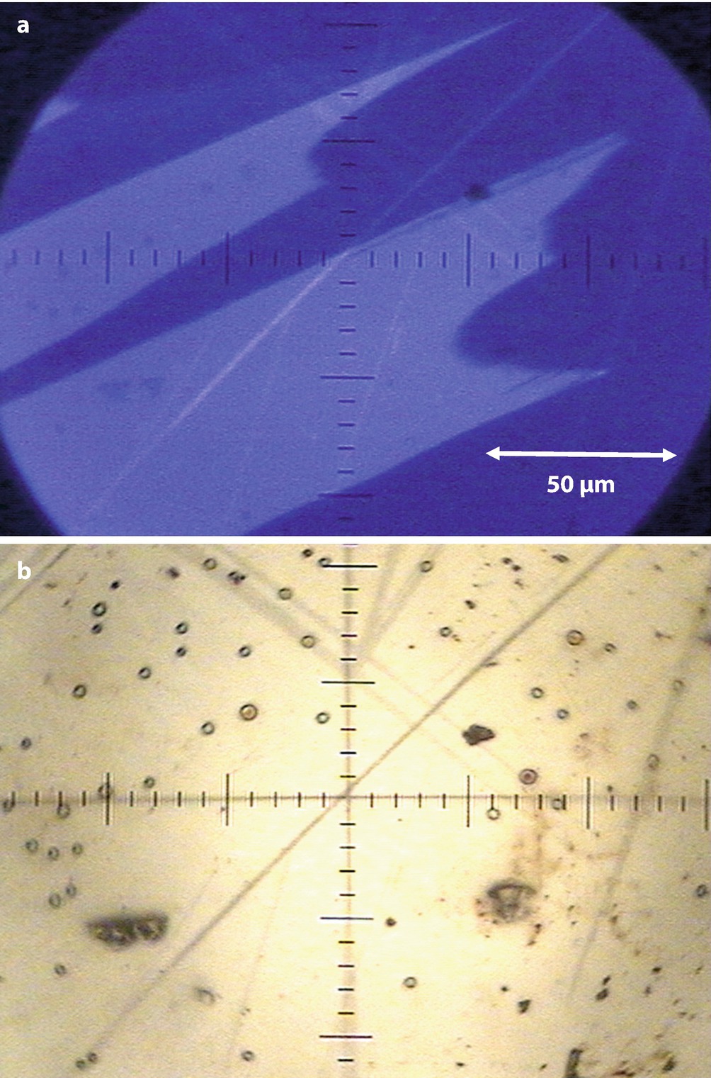
a CL emission from the mineral Benitoite (BaTiSi3O9) observed with a defocused 220-μm-diameter beam with 500 nA of beam current at E 0 = 20 keV. b Corresponding white light illumination image with the electron beam blanked into a Faraday cup

28.2.1 Collection of CL

To maximize photon collection, the specimen can be surrounded by a mirror configured to collect a solid angle of nearly 2π sr. An example shown in ◘ Fig. 28.6 of an ellipsoidal mirror in which the specimen is placed at one mirror focus, where an aperture permits the electron beam to reach the specimen, and the collector, typically a fiber optic, is placed at the other focus. For the examples of direct observation of CL shown in ◘ Figs. 28.4 and 28.5, the CL emission was collected through the high collection angle optical microscope integrated into an electron optical column (specifically, an electron probe microanalyzer configuration with wavelength dispersive spectrometry, EPMA/WDS, in which the optical microscope serves as the critical positioning aid for the WDS optimization).
../images/271173_4_En_28_Chapter/271173_4_En_28_Fig6_HTML.jpg
Fig. 28.6

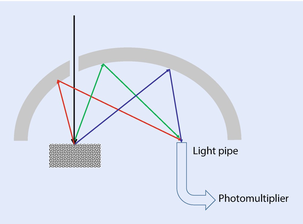
Schematic diagram of a high efficiency CL collection optic based upon an ellipsoidal mirror

28.2.2 Detection of CL

The photomultiplier (PM) is a useful detector for CL because of its sensitivity to photons in the energy range of interest, its fast response (hundreds of picoseconds to nanoseconds), and its operation as a high gain (gain ~106), low noise amplifier. The choice of the photocathode material, which converts the photons to low energy electrons at the first stage of the electron cascade, determines the spectral response, quantum efficiency, and sensitivity as a function of photon energy, typically showing a strong dependence as a function of wavelength. By choosing different photocathodes, PMs can be optimized for efficiently detecting different photon energies. ◘ Figure 28.7 illustrates a dispersive system in which the CL is scattered by a grating onto an array of PMs optimized to detect the different photon energies. Such a parallel detection strategy is critical to optimize measurements from weakly emitting systems, as well as to study systems with complex emission.
../images/271173_4_En_28_Chapter/271173_4_En_28_Fig7_HTML.png
Fig. 28.7

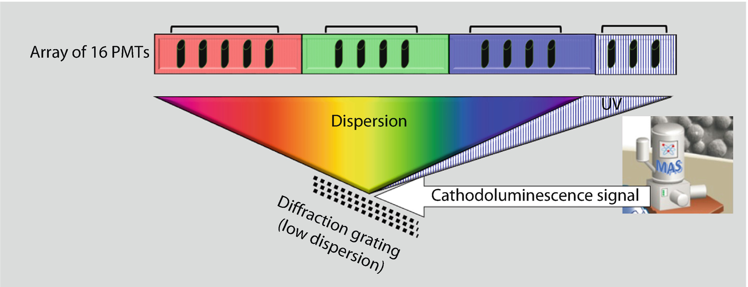
Schematic diagram of a dispersive CL system with an array of photomultpliers to sample a broad range of CL photon energies in parallel (courtesy of Gatan, Inc.)

Another detection scheme makes use of a single wide energy response photomultiplier to detect CL photons across the energy range. To separate the different color components of the CL emission, repeated scans of the area of interest are made with color filters (red, green, and blue) in the optical path to the PM, and the R-, G-, and B-images are combined.

Systems in which the photons are passed into a scanning optical spectrometer make possible detailed study of the CL emission in a single channel mode of operation.

28.3 Applications of CL

28.3.1 Geology

28.3.1.1 Carbonado Diamond

Carbonado is a rare variety of black diamond found in porous aggregates of fine polycrystals.

◘ Figure 28.8 shows CL imaging (using RGB filters) of a carbonado sample where the polycrystalline diamonds interacted with trace uranium during the Precambrian. The resulting MeV radiation damage is evident as metamict halos leaving the defects in the diamond structure (Magee et al. 2016). These haloes were not evident in SEM SE or BSE images or in elemental maps, indicating the sensitivity of CL emission to the presence of lattice defects that do not otherwise significantly affect the electron beam specimen interaction.
../images/271173_4_En_28_Chapter/271173_4_En_28_Fig8_HTML.jpg
Fig. 28.8

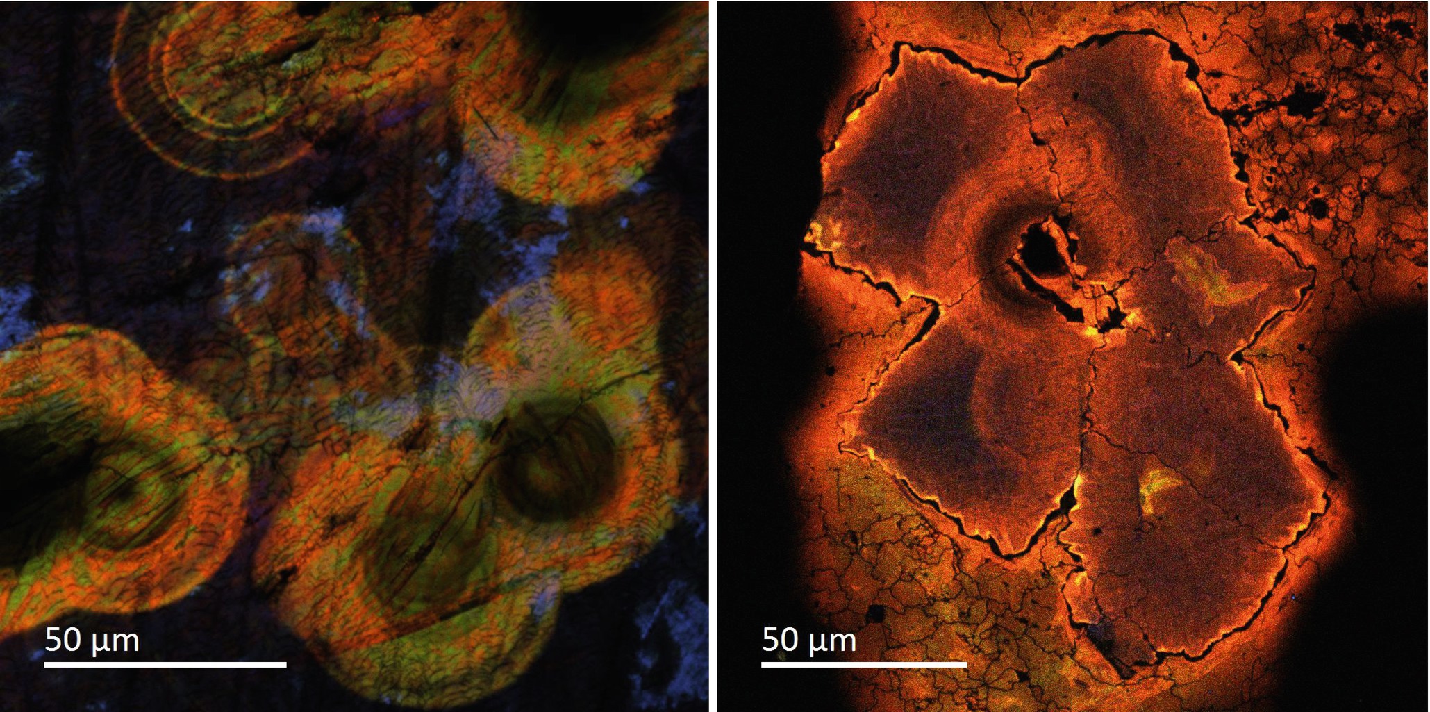
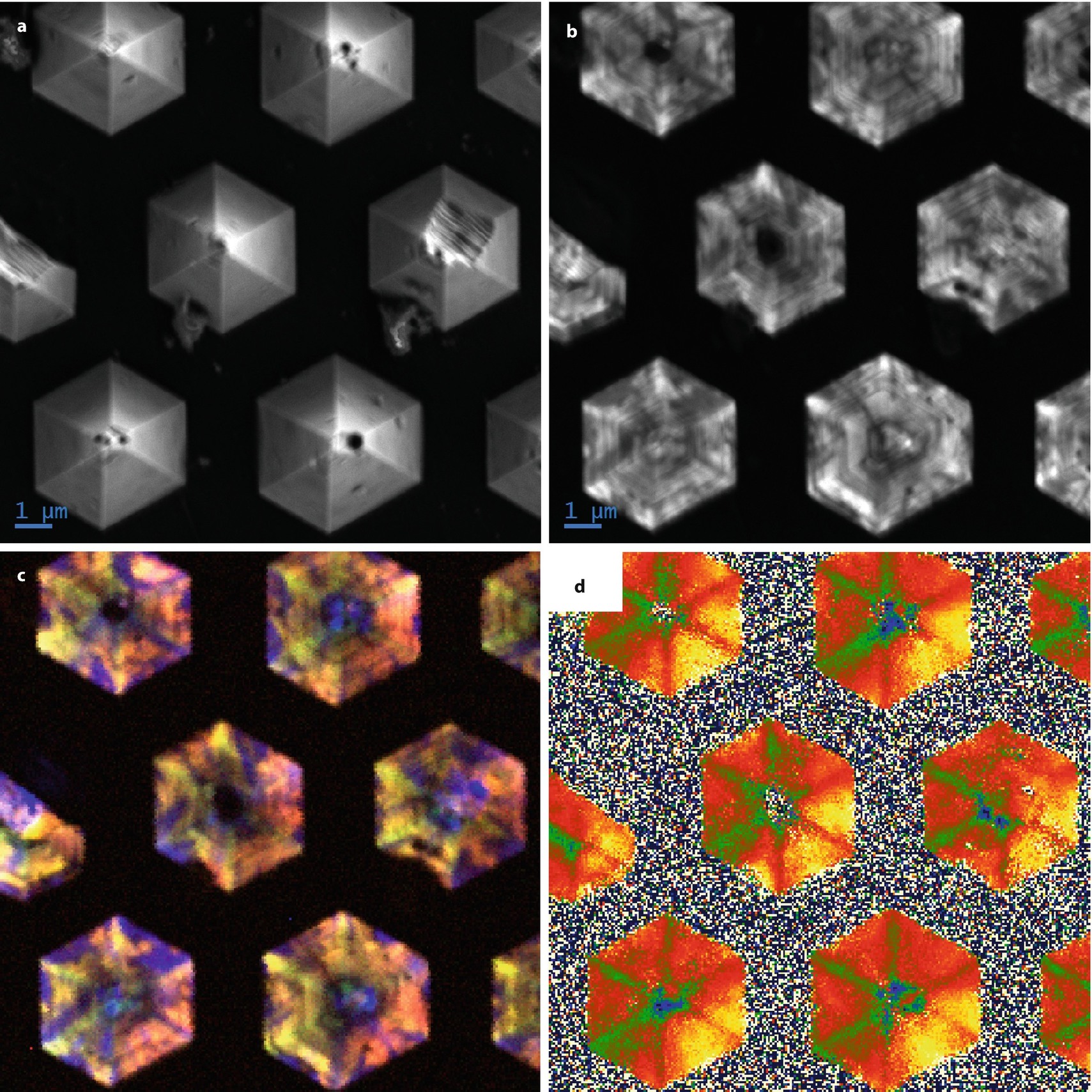
CL imaging (RGB) of a carbonado, a rare variety of diamond. The polycrystalline material interacted with uranium during the Precambrian and MeV radiation damage is evident as metamict halos leaving the defects in the diamond structure (Magee et al. 2016) (Images courtesy of E. Vicenzi (Smithsonian Institution))

28.3.1.2 Ancient Impact Zircons

◘ Figure 28.9 shows CL imaging (using RGB filters) of an impact zircon collected using E 0 = 20 keV and 5-keV beam energies. The details of zircon disproportionation to ZrO2 and silicate glass, as well as the zircon interior, are more evident at using a low energy beam (Zanetti et al. 2015).
../images/271173_4_En_28_Chapter/271173_4_En_28_Fig9_HTML.jpg
Fig. 28.9

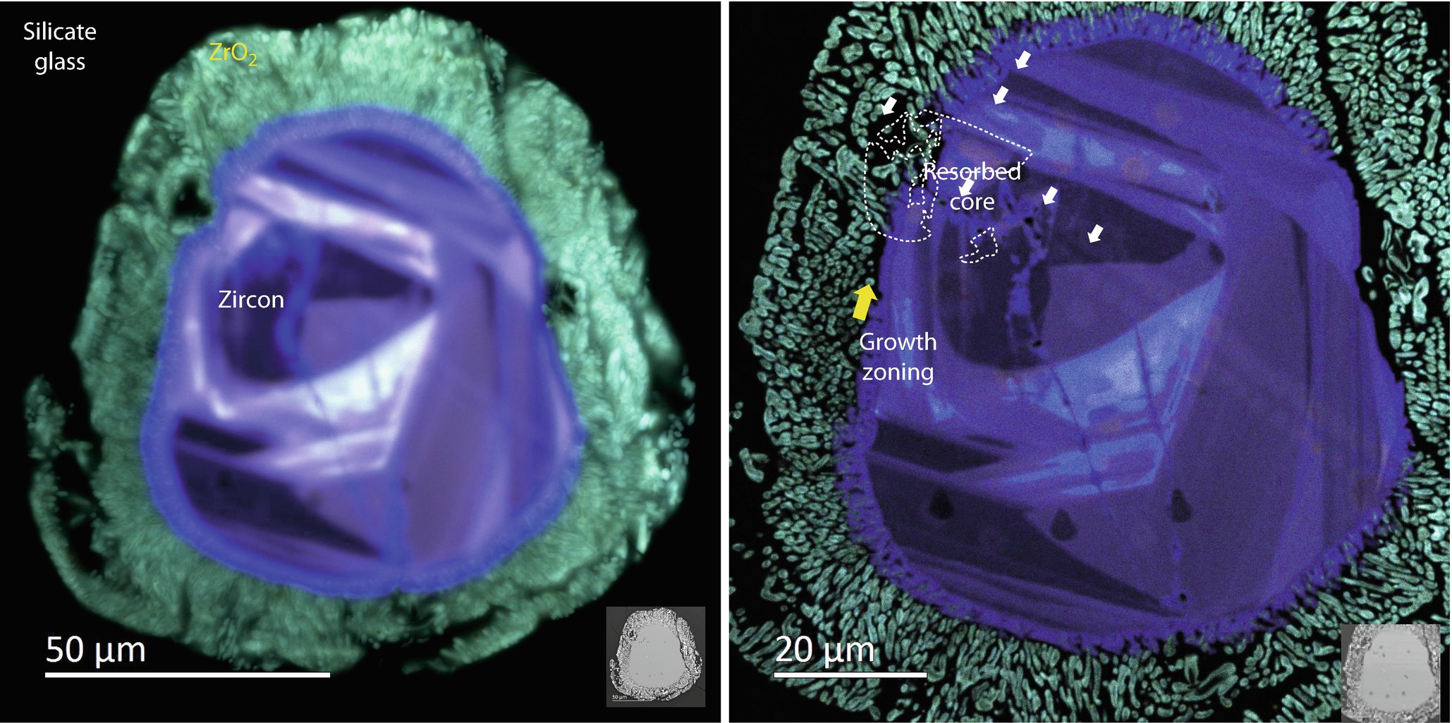
CL imaging (RGB) of an impact zircon collected using E 0 = 20 keV (left) and 5 keV (right). The details of zircon disproportionation to ZrO2 and silicate glass, as well as the zircon interior, are more evident using a low energy beam (Zanetti et al. 2015) (Images courtesy of E. Vicenzi (Smithsonian Institution))

28.3.2 Materials Science

28.3.2.1 Semiconductors

As an example of the detailed information that can be obtained with CL spectrometry, ◘ Fig. 28.10 shows a study of hexagonal GaN structures grown on a silicon substrate with a patterned mask to define the shape, as shown in the SEM image (E 0 = 2 keV) (◘ Fig. 28.10a). The panchromatic CL image formed by the integrated intensity of all measurable wavelengths (◘ Fig. 28.10b), reveals crystal defects which are observed as dark regions in the CL image including: (i) planar defects which can be seen as dark lines where they intersect the face(s) of the pyramid and (ii) regions with a high concentration of point defects or impurities. CL spectrum imaging was used to map the near band edge emission of GaN as a 3D datacube where a full CL spectrum (1D) was acquired at every pixel in the region of interest (2D). Changes in the near band edge emission were investigated by spectral peak fitting. The derived central wavelength map reveals the strain level of the material with noticeable shifts appearing along the pyramid ridges. The RGB composite image is created from: high strain state GaN (yellow), low strain state (purple), defect (red).
../images/271173_4_En_28_Chapter/271173_4_En_28_Fig10_HTML.jpg
Fig. 28.10

CL study of GaN structures grown on Si: a SEM SE image (E 0 = 2 keV); b panchromatic CL image; c CL spectrum image data analyzed to derive the central wavelength value; d RGB composite (Example courtesy of D. Stowe, Gatan, Inc.)

28.3.2.2 Lead-Acid Battery Plate Reactions

It is possible to detect relatively strong CL signals with modified BSE detectors, as most of these solid state detectors are very sensitive to light. The challenge is to exclude BSE from the detected signal. The easiest way to do this is to coat a glass coverslip with a conductive transparent material like indium tin oxide (ITO). The glass cover slip prevents the electrons from interacting with the solid state detector and the conductive transparent coating prevents charging while allowing the CL signal to reach the detector.

It is interesting to note that some of the low vacuum or variable pressure SEMs that are commercially available use the CL light generated by the interaction of the secondary electrons with the gas in the chamber to produce a signal during variable pressure operation. One can use the same detector system, which consists of a glass light guide located near the sample that is coupled to a photomultiplier, for direct detection of CL emission. This type of detector is sensitive to low levels of light and thus when used in high vacuum mode can be a very simple but effective CL detector.

During the charging and discharging of lead acid battery plates, a variety of lead containing phases can form on the surface of the lead plate. Two important phases are lead sulfide (PbS) and lead sulfate (PbSO4). Note that these compounds are similar in backscattering making it difficult to determine PbS from PbSO4 in images. ◘ Figure 28.11a shows a secondary electron image of the surface of a lead plate after it has been exposed to conditions that may occur in a lead-acid battery. Numerous euhedral crystals were observed on the surface of the lead plate. The EDS spectra indicated Pb and S as the major constituents and possibly O. Oxygen can be detected in the EDS spectrum of PbSO4 from an ideal flat specimen, as shown in the DTSA-II simulation in ◘ Fig. 28.11c, but because of the high absorption from Pb, the time requirement for mapping O to locate PbSO4 becomes prohibitive. Moreover, given the complex topography of the sample shown in ◘ Fig. 28.11a, mapping oxygen is likely to be badly compromised by strong X-ray absorption artifacts from the topography. CL can be of great use in this system as PbS does not exhibit CL while PbSO4 strongly exhibits CL, enabling these compounds to be rapidly distinguished. In order to determine the likely compound, a simple CL system consisting of a light guide attached to a photomultiplier tube was used. ◘ Figure 28.11b is an image obtained using this simple CL detector. Note that the euhedral crystals strongly exhibit CL, and this clearly indicates that these crystals are most likely PbSO4 and not PbS.
../images/271173_4_En_28_Chapter/271173_4_En_28_Fig11_HTML.png
Fig. 28.11

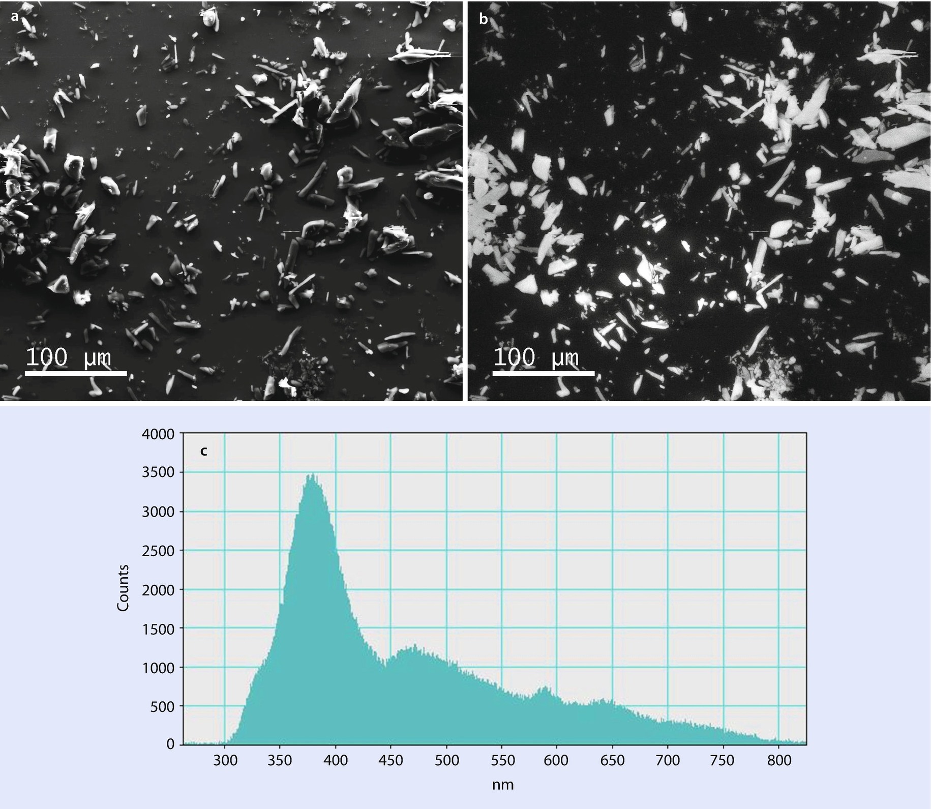
a SEM SE image of deposits on lead-acid battery. b CL image of the same area; c DTSA-II simulation of the EDS spectra of PbS and PbSO4 from an ideal flat surface at E 0 = 15 keV (courtesy of Sandia National Laboratory)

28.3.3 Organic Compounds

Despite the general vulnerability of organic compounds to radiation damage under electron bombardment, some organic compounds can be examined with CL spectrometry. ◘ Figure 28.12 shows an SEM SE image and a panchromatic CL image of acetaminophen (paracetamol, N-(4-hydroxyphenyl)ethanamide N-(4-hydroxyphenyl)acetamide) along with a CL spectrum showing broad CL bands.
../images/271173_4_En_28_Chapter/271173_4_En_28_Fig12_HTML.jpg
Fig. 28.12

Acetaminophen, E 0 = 20 keV: a SEM SE image; b panchromatic CL image; c CL spectrum (Example courtesy of S. Wight, NIST)

Creative Commons

Open Access This chapter is licensed under the terms of the Creative Commons Attribution-NonCommercial 2.5 International License (http://creativecommons.org/licenses/by-nc/2.5/), which permits any noncommercial use, sharing, adaptation, distribution and reproduction in any medium or format, as long as you give appropriate credit to the original author(s) and the source, provide a link to the Creative Commons license and indicate if changes were made.

The images or other third party material in this chapter are included in the chapter's Creative Commons license, unless indicated otherwise in a credit line to the material. If material is not included in the chapter's Creative Commons license and your intended use is not permitted by statutory regulation or exceeds the permitted use, you will need to obtain permission directly from the copyright holder.