Joseph I. Goldstein, Dale E. Newbury, Joseph R. Michael, Nicholas W.M. Ritchie, John Henry J. Scott and David C. JoyScanning Electron Microscopy and X-Ray Microanalysishttps://doi.org/10.1007/978-1-4939-6676-9_30
30. Focused Ion Beam Applications in the SEM Laboratory
Joseph I. Goldstein1, Dale E. Newbury2, Joseph R. Michael3, Nicholas W. M. Ritchie2, John Henry J. Scott2 and David C. Joy4
(1)
University of Massachusetts, Amherst, Massachusetts, USA
(2)
National Institute of Standards and Technology, Gaithersburg, Maryland, USA
(3)
Sandia National Laboratories, Albuquerque, New Mexico, USA
(4)
University of Tennessee, Knoxville, Tennessee, USA
30.1 Introduction
The use of focused ion beams (FIB) in the field of electron microscopy for the preparation of site specific samples and for imaging has become very common. Site specific sample preparation of cross-section samples is probably the most common use of the focused ion beam tools, although there are uses for imaging with secondary electrons produced by the ion beam. These tools are generally referred to as FIB tools, but this name covers a large range of actual tools. There are single beam FIB tools which consist of the FIB column on a chamber and also the FIB/SEM platforms that include both a FIB column for sample preparation and an SEM column for observing the sample during preparation and for analyzing the sample post-preparation using all of the imaging modalities and analytical tools available on a standard SEM column. A vast majority of the FIB tools presently in use are equipped with liquid metal ion sources (LMIS) and the most common ion species used is Ga. Recent developments have produced plasma sources for high current ion beams. The gas field ion source (GFIS) is discussed in module 31 on helium ion microscopy in this book.
This chapter will first review ion/solid interactions that are important to our use of FIB tools to produce samples that are representative of the original material. This discussion will then be followed by how FIB tools are used for specialized imaging of samples and how they are used to prepare samples for a variety of SEM techniques.
30.2 Ion–Solid Interactions
It is important to understand some of the ion-solid interactions that occur so that the user can appreciate why certain methods and procedures are followed during sample preparation. There are many events that occur when an energetic ion interacts with the atoms in a solid, but for the case of SEM sample preparation and ion imaging we are mainly interested in sputtering, secondary electron production and damage to the sample in terms of ion implantation and loss of crystalline structure. Sputtering is the process that removes atoms from the target. Secondary electron production is important as images formed with secondary electrons induced by ions have some important advantages over electron-induced secondary electron imaging. Finally, it is important to realize that it is impossible to have an ion beam interact with a sample without some form of damage occurring that leaves the sample different than before the ion irradiation.
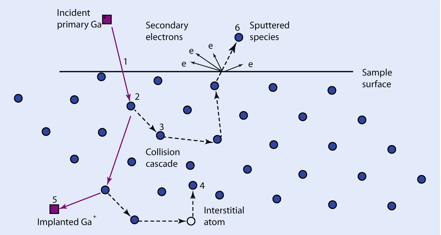
A schematic diagram of the interactions is shown in ◘ Fig. 30.1. Here an energetic ion is injected into a crystalline sample. The ion enters the sample at position 1. The ion is then deflected by interactions with the atomic nuclei and the electron charges. As the ion moves through the sample it has sufficient energy to knock other atoms off their respective lattice positions as shown at position 2. The target atoms that are knocked off their atomic positions can have enough energy to knock other target atoms off their atomic positions as shown at position 3. Some of the atoms that have been knocked from their atomic positions may reoccupy a lattice position or may end up in interstitial sites. There can also be lattice sites that are not reoccupied by target atoms and are left as vacancies. Both interstitials and vacancies are considered damage to the crystalline structure of the sample as shown in position 4. Most of the time, the original beam ion will end up coming to rest within the sample. This is termed ion implantation and is shown at position 5. Ion implantation results in the detection of the ion beam species in the sample. Many of the collision cascades will eventually reach the surface of the sample. Sufficient energy may be imparted to knock an atom from the surface into the vacuum. This process is called sputtering and results in a net loss of material from the sample as shown in position 6. At the same time when the ion is either entering or leaving the sample, secondary electrons are generated that are useful for producing images of the sample surface scanned by the ion beam. It is important to remember that scanning an energetic ion beam over the surface of the sample will always result in some damage to the sample. Understanding the interaction of ions with the target material is helpful in reducing the amount of damage to acceptable or tolerable levels through appropriate sample preparation techniques. For a complete review of ion–solid interactions see Nastasi et al. (1996).
Fig. 30.1
Schematic of some of the important ion–solid interactions that can occur
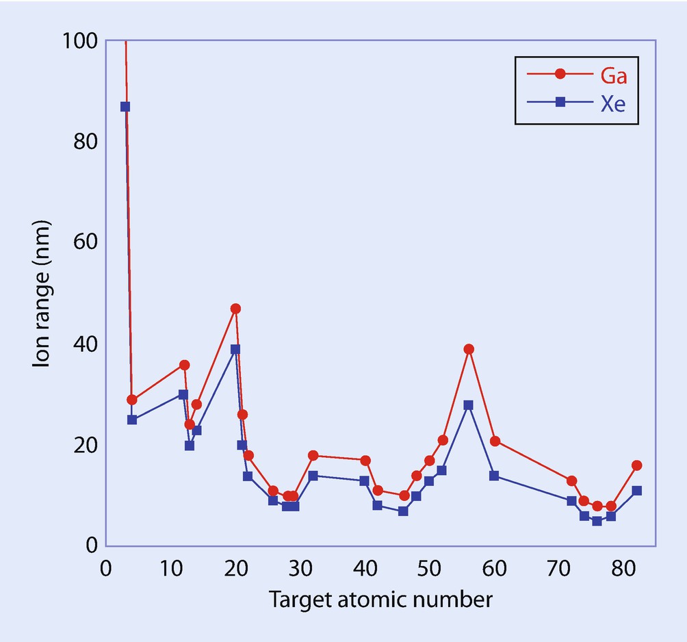
In module 1 on electron–beam specimen interactions, the range that an electron travels in a sample is discussed. Generally for medium-energy electrons (15–20 keV) the electron range in the transition elements is on the order of 1 μm. The ranges of heavy ions like Ga and Xe are extremely short when compared to electron ranges for similar energies. ◘ Figure 30.2 is a plot of the ion ranges for Xe and Ga as a function of the atomic number of the target material. Note that the range for either Ga or Xe ions with an energy of 30 keV is generally much less than 50 nm. Thus, ions travel very short distances in solid targets and as a result the near surface region of the sample is where the ion interactions take place and where we expect to see the crystalline sample damage discussed in ◘ Fig. 30.1 (Nastasi et al. 1996; Ziegler and Biersack 1985).
Fig. 30.2
Calculated range for 30-kV Xe and Ga ions as a function of atomic number
30.3 Focused Ion Beam Systems
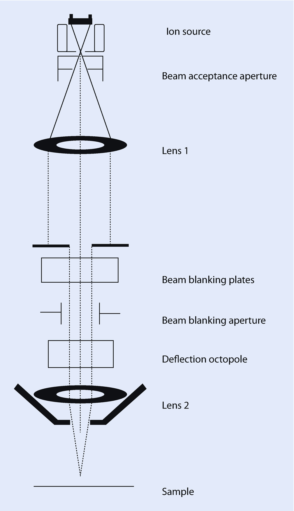
Modern focused ion beam tools are almost always two-column systems with a FIB column and an SEM column mounted on one chamber and both columns focused precisely on the same region of the sample. This allows one to use the SEM column to monitor the progress of the FIB milling that is being performed and to image the sample immediately after preparation. This arrangement also enables the use of sequential FIB milling and SEM imaging leading to the capability to produce 3D data sets. There are still some highly specialized uses for single beam FIB tools; for example, integrated circuit modification is done generally with single beam FIB tools. Modern FIB systems utilize either a LMIS source or a plasma source to produce ion beams with variable current to allow both large volume removal and fine scale polishing of the sample. Both the LMIS and the plasma source have advantages and disadvantages. The most common LMIS produces Ga ions, while it is common for the plasma sources to utilize inert gases like Ne, Ar, or Xe. Ga ion sources have higher brightness as compared to the plasma sources and thus have higher current densities in the focused ion spots. Ga is a fairly reactive element, however, and may result in artifacts when implanted into some materials. Plasma sources have lower brightness but higher overall current than the LMIS sources resulting lower current densities in the focused spot but much higher total current that allows much faster material removal rates when compared to LMIS ion sources. Both the LMIS and the plasma ion source utilize similar optics to produce focused scanning beams of ions. ◘ Figure 30.3 shows a schematic of a typical ion column. This column resembles a simple SEM column with the exception that the magnetic lenses that are used to focus electrons are not capable of focusing the heavier ions. For ions, the lenses are electrostatic and require high voltages to focus energetic ions due to their relatively large mass to charge ratio.
Fig. 30.3
Schematic of a typical focused ion beam column
Sample stages must be accurate and reproducible for easy and efficient FIB processing of samples. There can be multiple stage moves during the preparation of samples in a FIB tool and each move should be reproducible so that the operator can easily return to the region of interest. Stage accuracy and reproducibility has become more important as automated routines have become common place during the production of samples or during sequential milling and imaging operations (Giannuzzi 2006; Orloff et al. 2003).
30.4 Imaging with Ions
Although FIB is usually used to remove material via sputtering, ions produce a large yield of secondary electrons. The secondary electrons signal can be collected and imaged just like secondary electrons produced with an electron beam, which means we can use all of the detectors that we are very familiar with from electron beam imaging. This leads to the use of the FIB as an imaging tool sometimes referred to as scanning ion microscopy. Secondary electrons produced with ions are referred to as ion induced secondary electrons (iSE). FIB columns are all equipped with one or more iSE detectors with the most common one being the ET detector as used in the SEM. iSE imaging has some advantages over SE imaging in the SEM. First, the ion beam produces many more SEs per incident particle than does a similar current electron beam resulting in a high signal, low noise image. Also, it is interesting to note that the iSE signal collected in a FIB is free of the backscattered electron component that reduces contrast in electron beam induced SE images. iSE imaging of surfaces shows topographical contrast that is familiar to anyone who has operated an SEM. iSE imaging of crystalline samples can produce very striking high contrast grain images due to the higher propensity for ions to channel along specific crystal planes resulting in a varying iSE yield as a function of grain orientation.
During ion imaging of a sample there are other signals produced that are of limited use. The interaction with the sample causes secondary ions to be ejected from the sample. These can be used to form images. However there are few secondary ions produced as compared to the iSE and therefore the signals tend to be noisy requiring either longer scan times or higher beam currents to be used, both of which will result in increased levels of sample damage during imaging.
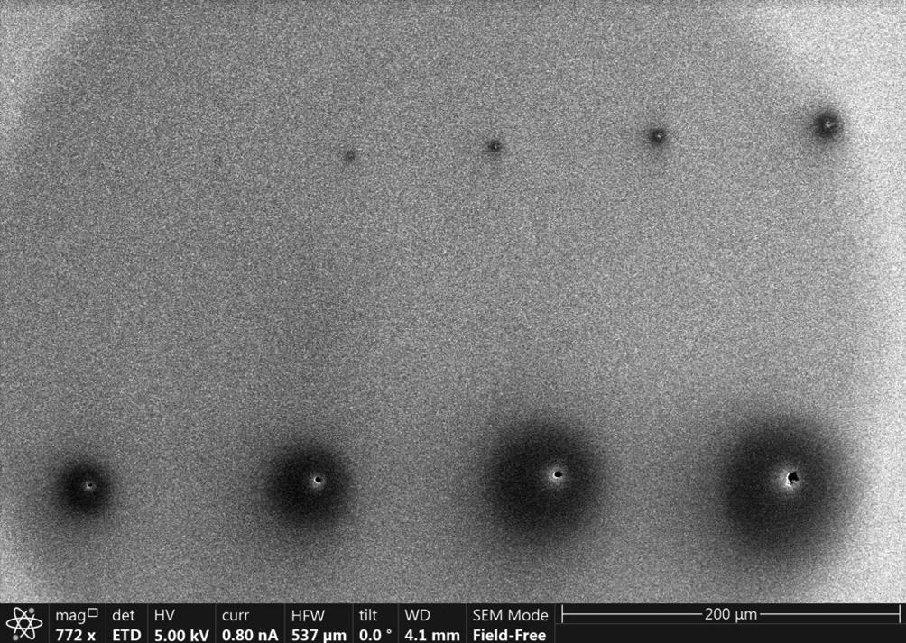
Resolution of scanning ion microscope images is not just a function of the beam size that is generated by the ion column. The ultimate resolution of a scanning ion image is a convolution of the beam size and some measure of the rate at which the sample is milled. Resolution is worse for materials that mill quickly and better for those materials that have a slower sputter rate (Orloff et al. 1996, 2003). Just like the SEM, as the current in the probe is increased, the beam size increases. ◘ Figure 30.4 shows spot burns from an LMIS (Ga) column where the ion beam is put in spot mode and left stationary so that the substrate is milled away. The beam size is then some measure of the size of the spot including the halos around the milled area as ion beams suffer significant aberrations as occur with lenses in the SEM. In both the LMIS and the plasma cases, the ion columns are capable of producing symmetric ion beams with the exception that at the larger currents various optical aberrations become dominating and result in a less well defined ion beams.
Fig. 30.4
Spot burns on a tungsten coated silicon wafer. The beam was held stationary at each point for 10 s. Top row from left to right: 24 pA, 80 pA, 0.23 nA, 0.43 nA, 0.79 nA, and 2.5 nA. Bottom row from left to right: 9 nA, 23 nA, 47 nA and 65 nA (Bar = 200 µm)
The collection of secondary ions requires an additional detector that is sensitive to secondary ions and can reject the signal produced by the secondary electrons. These secondary ion detectors are often now optional on modern instruments. ◘ Figure 30.5 is a comparison between secondary electron imaging induced by electrons and secondary ion imaging induced by ion scanning. The sample consists of a tungsten wire and a human hair. The electron image shows good surface detail, but the uncoated hair is charging and the surface information is somewhat obscured. The secondary ion image shows no charging artifacts on the human hair but also shows an increased level of surface detail due to the small escape length of the secondary ions. One must always remember that imaging with ions will always cause some level of damage within the sample (Giannuzzi 2006; Mayer 2007; Michael 2011).
Fig. 30.5
Images of a tungsten wire (left) and a human hair (right). a Secondary electron image induced by 5-kV electrons. b Ion induced secondary ion images with 30-kV Ga ions. Note the reduced charging in the ISE image and the increased surface detail visible in the secondary ion image
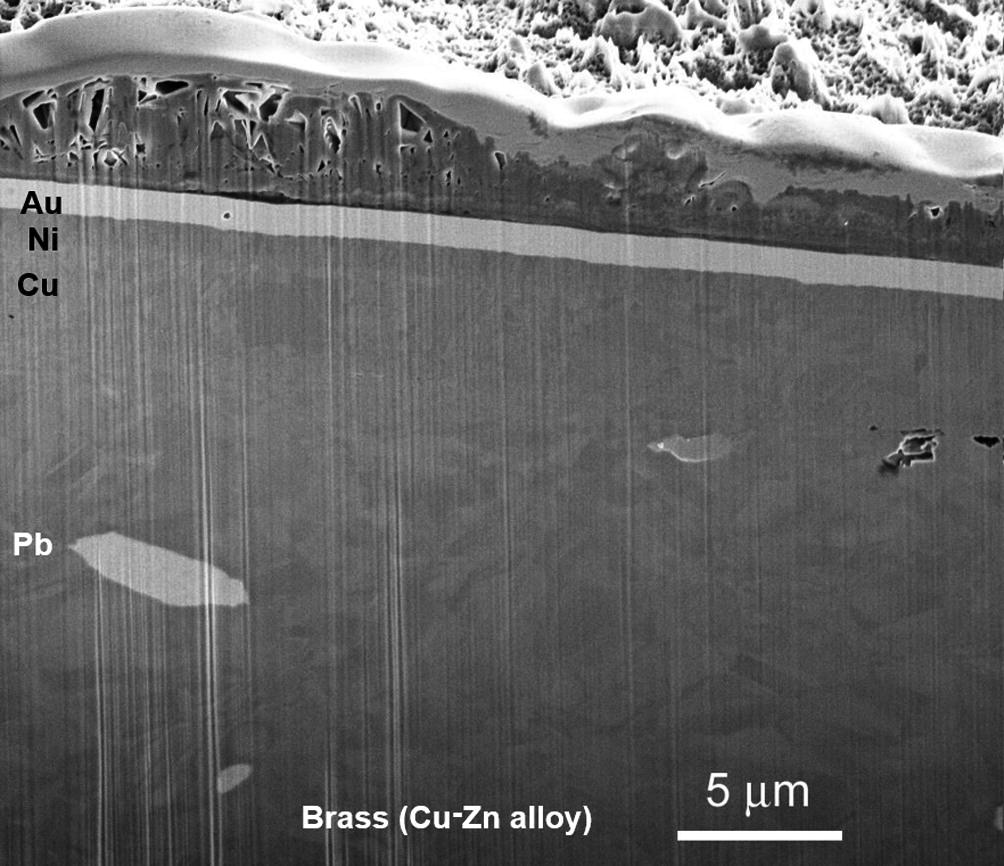
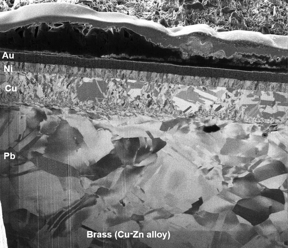
◘ Figure 30.6 is an electron-induced secondary electron (SE) image of free-machining brass coated with layers of Cu, Ni, and Au. Note that free-machining brass contains particles of Pb. ◘ Figure 30.6 shows the contrast that we have come to expect from electron beam induced SE imaging. The higher atomic number regions appear brighter as a result of higher secondary electron yield that results from the SE2 contributions from the unavoidable backscattered electrons (BSEs). ◘ Figure 30.7 is an iSE image (30 kV Ga) of the identical area of the sample. The various layers are immediately obvious because the ion channeling contrast is quite strong and the grain structure of each layer is revealed. It can also be observed that the Pb region and the Au layer are no longer bright relative to the brass as in ◘ Fig. 30.6. ◘ Figure 30.7 demonstrates that the iSE yield is not a simple function of the target atomic number (Joy and Michael 2014). Also, ◘ Fig. 30.7 demonstrates the very strong grain contrast that can be observed in many crystalline materials. This grain contrast is due to the way that the crystallography of the sample impacts the penetration depth of the primary beam ions and therefore the iSE yield. Small changes in the ion beam incident angle can change the grain contrast that is observed. Thus, if you are trying to determine the nature of the contrast that is observed in a crystalline sample it is a simple matter to tilt the sample 2–4° and observe how the contrast changes. If the contrast is due to ion channeling then the contrast between grains should change (Giannuzzi and Michael 2013).
Fig. 30.6
Electron beam (5-kV) induced secondary electron imaging of a free-machining brass (Cu-Zn alloy) that has been coated with layers of Cu, Ni and Au. Note that the various layers are faintly visible and that the contrast is as expected with the highest atomic number region (Pb) brighter than the brass or the Cu and Ni. Au also appears bright
Fig. 30.7
Ion beam (30-kV) induced secondary electron imaging of a free-machining brass (Cu-Zn alloy) that has been coated with layers of Cu, Ni and Au. Note that the various layers are much more easily visualized due to the high contrast crystallographic contrast. Also, note that the brightness of the phases can no longer be interpreted strictly by atomic number. Here the Pb and the Au regions appear with lower signal levels than does the brass or the Cu and Ni layers
30.5 Preparation of Samples for SEM
FIB–based sample preparation for SEM is a large field due to the versatility of modern SEMs and the many techniques that are utilized. One of the most common uses of FIB is for subtractive processing of the sample in that the FIB is used to sputter site specific regions of the sample to produce cross sections. It is also common to produce samples that are manipulated from the bulk for study. One example is the extraction and production of thin samples for transmission Kikuchi diffraction as discussed in module 29 on electron backscatter diffraction. FIB has become an indispensable tool in the production of electron transparent samples for STEM/TEM and now the FIB can produce samples that are sufficiently thin for transmission imaging in the SEM at 30 keV using the STEM-in-SEM technique. FIB sample preparation is applicable to many materials classes that are imaged in the SEM including polymers, metal, semiconductors, and ceramics.
30.5.1 Cross-Section Preparation
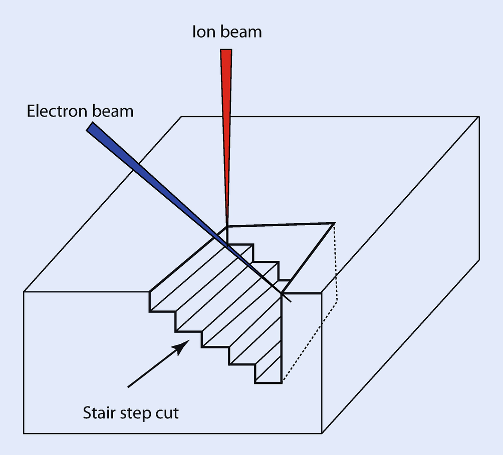
In materials characterization it is often of interest to image a section of the sample that is not visible from a planar section. In this case, the FIB is used to mill away material to expose a cross sectional view of the sample, as shown schematically in ◘ Fig. 30.8. There are many ways to accomplish this and in many modern FIB tools this process is fully automated and the user must simply indicate where the cross section is to be made. The following example will show the steps that are needed for a cross section to be produced.
Fig. 30.8
Schematic of an FIB-prepared cross section. A stair-step is milled using the ion beam and then the exposed section that is perpendicular to the original sample surface is polished with a series of lower current ion beams. The cross section can be immediately imaged with the SEM beam that is at some inclined angle with respect to the ion beam
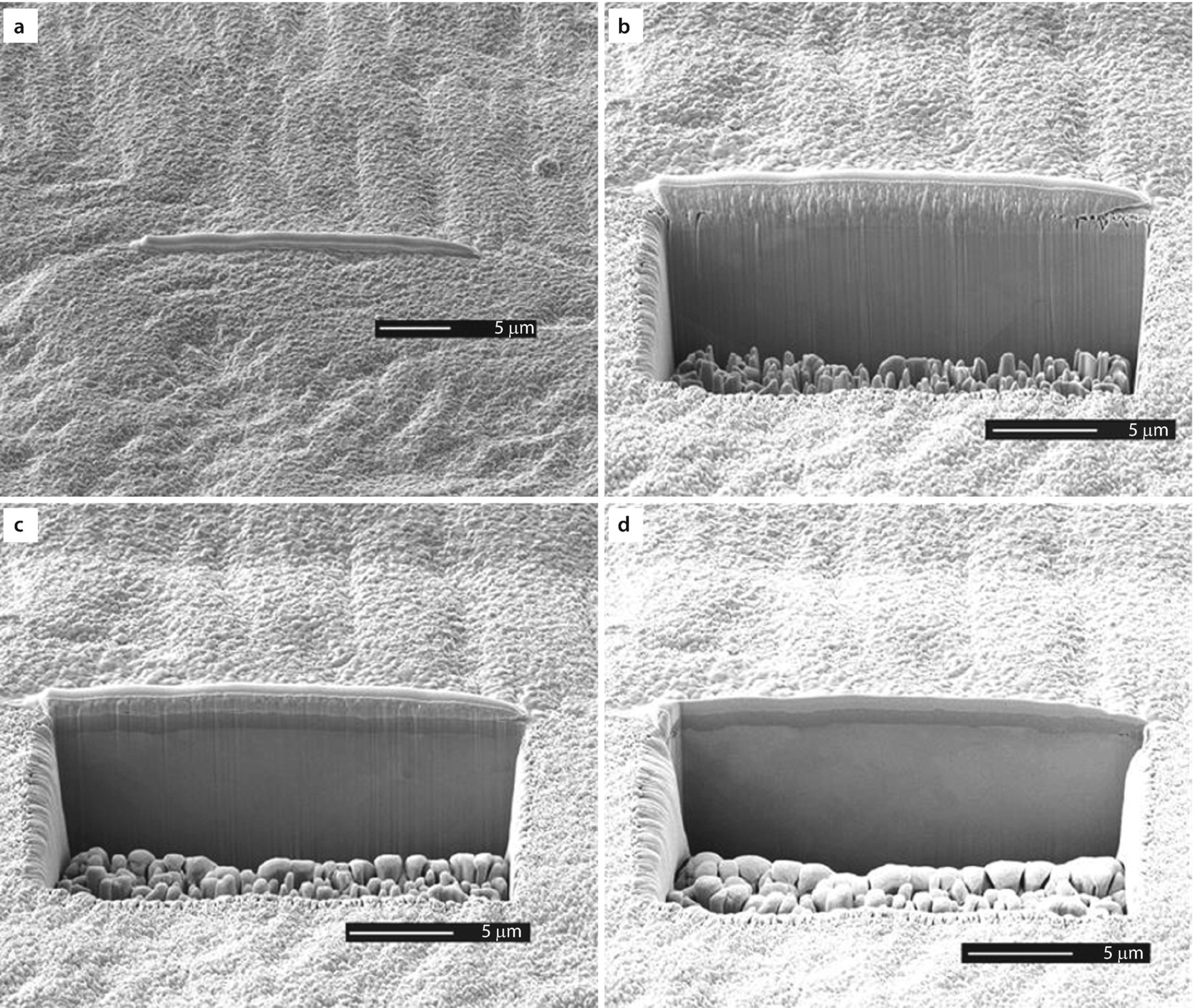
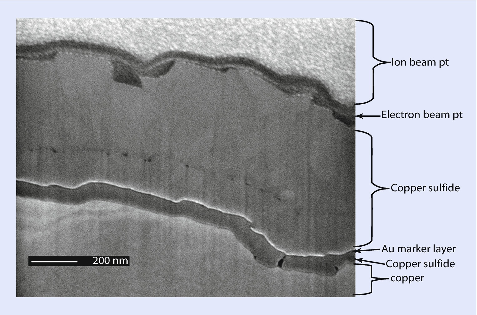
As was discussed earlier, any time the sample is exposed to the ion beam damage will occur. It is necessary to image the sample during preparation so the easiest way to eliminate the damage to the sample from the beam is to place a protective layer over the area to be cross sectioned. FIB tools come equipped with gas injectors that can be used during sample preparation. Common precursor gasses used can deposit tungsten, platinum, or carbon. Each of these materials works quite well to protect the region of interest from the ion beam. The precursor gasses are delivered to the sample surface through a small needle that is placed in very close proximity to the area of interest. Either the ion beam or the electron beam can be scanned over the area of interest. Some of the gas molecules that are delivered through the needle absorb on to the sample surface where combined action of the primary beam (electron or ion) and the secondary electrons produced by the interaction of the beam with the sample decomposes the absorbed gas. This leaves behind a deposit that contains the desired material but also includes the ion beam species (if ions were used) and some residual organics from the precursor. Due to the short range of ions in materials, the protective layer need not be very thick; but typically most applications use about 1 μm to provide protection and for ease of subsequent milling of the sample. ◘ Figure 30.9 shows a cross section produced in a sulfide copper test coupon where the objective of the experiment was to measure the rate of sulfide growth in accelerated aging conditions. The first step (◘ Fig. 30.9a) is to deposit the protective platinum layer on the area to be sectioned. The goal is to have the completed cross section positioned under the platinum protective layer. A coarse first cut is made with a large current ion beam, the result of which is shown in ◘ Fig. 30.9b. Although the cross section is relatively clean at this point it is not adequate for quality SEM imaging. Further polishing of the cross section is completed with lower current ion beams in this case ◘ Fig. 30.9c was completed with a 1-nA ion beam and ◘ Fig. 30.9d is the cross section after final polishing with a 300-pA ion beam. The total time to produce this cross section is about 20 min. The completed cross section imaged at higher resolution is shown in ◘ Fig. 30.10. Note that all of the important microstructural features are easily observed in this very smooth polished cross section.
Fig. 30.9
Required steps to making a quality cross section of the surface of a corroded copper test coupon in the FIB. a Deposition of platinum protective layer. b Coarse milling of the cross section with a 7-nA Ga ion beam. c Further polishing with a 1-nA Ga ion beam d Final polishing with a 300-pA Ga ion beam to produce the completed cross section
Fig. 30.10
High resolution image of the sulfide layer on the top of the test coupon sectioned in ◘ Fig. 30.9. Note the surface smoothness and the feature sizes that can be observed on the ion milled section
FIB prepared surfaces can be very smooth and nearly featureless. The relative brightness between different materials can often provide sufficient image contrast. Materials contrast by itself may be insufficient and a method to enhance the contrast may be needed. One way to do this is to introduce gasses near the sample that react with the ion beam and the sample surface to etch the FIB polished surface. One chemical that does this for semiconductor devices is trifluoracetic acid (TFA) that etches oxides and nitrides preferentially to silicon and metals. ◘ Figure 30.11 demonstrates the use of TFA for enhancing the contrast in FIB milled surfaces. The sample was prepared using standard cross sectioning procedures in the FIB. After cross sectioning the sample was rotated and tilted so that the milled surface was normal to the ion beam. A low beam current is selected and then the gas is introduced through a fine needle while the ion beam is scanned over the milled surface. While milling, the sample image provides an etching progress monitor so that the etching progress can be terminated when the correct degree of etching has been achieved.
Fig. 30.11
This figure demonstrates the enhancement of image contrast using a TFA as a beam assisted etchant. a As-milled cross section of a semiconductor device. Note the surface smoothness and the low contrast. b Same surface after beam assisted etching with TFA. Note that process adds a small amount of topography to the milled surface allowing the different materials to be more easily imaged
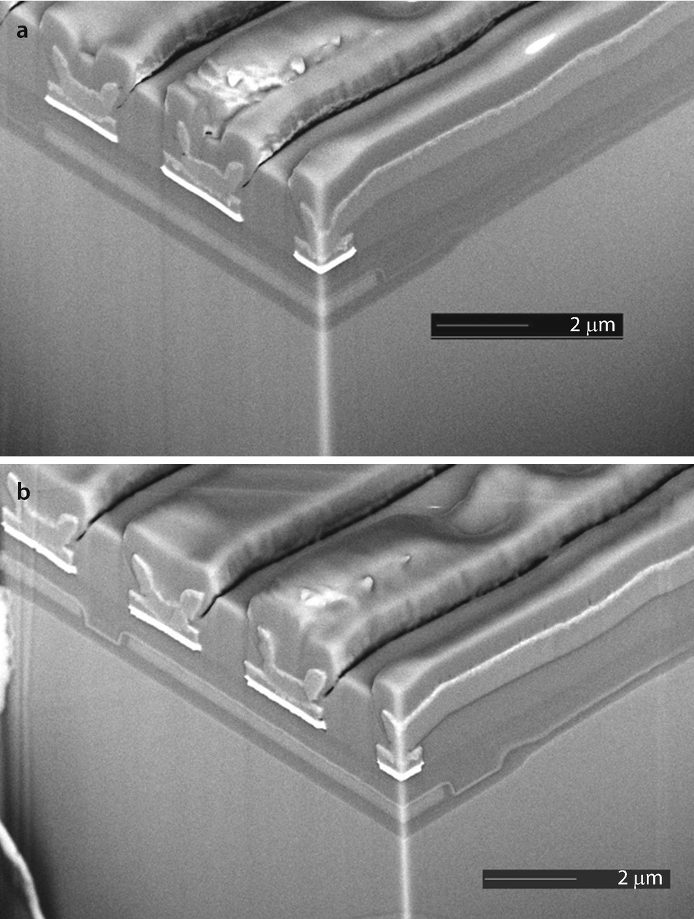
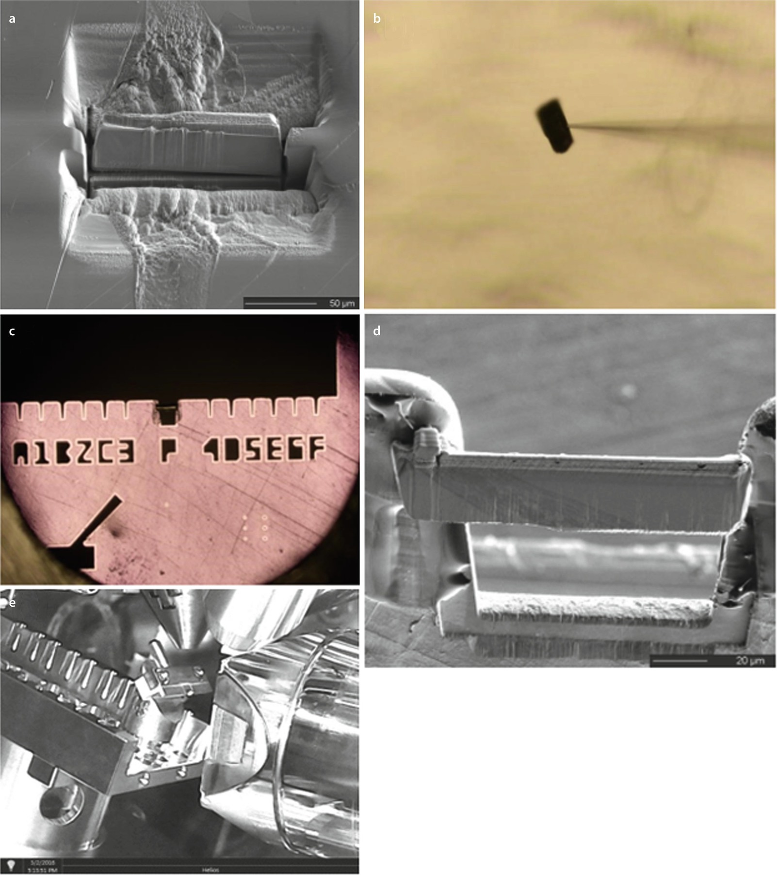
SEM applications of FIB sample preparation can also utilize samples that have been removed from the bulk material. This is generally done when the research requires EDS, EBSD, or STEM-in-SEM to be conducted as each of these techniques will not work optimally with standard cross sections (Prasad et al. 2003). Lift-out samples are made by milling trenches on both sides of the area of interest after a protective layer was deposited. The FIB beam is used to cut the sample free from the bulk material and then it can either be polished in the trench or lifted out to a support grid for subsequent polishing and if needed thinning to an acceptable thickness. Figure 30.12 shows some of the steps required to lift-out a 150-μm-wide sample. This was accomplished with a Xe plasma FIB but the steps are the same for a Ga FIB. Ex situ lift-out was used to remove the sample from the bulk followed by attachment to the Cu support structure to allow safe handling of the sample. Once the sample was attached to the support structure, final sample polishing was performed and the sample was ready for analysis. EBSD results obtained from the sample shown in ◘ Fig. 30.12 are shown in ◘ Fig. 30.13. Note that the sample surface is nearly ideal for EBSD as the number of mis-indexed or not indexed pixels is quite low.
Fig. 30.12
Gibeon meteorite sample produced by the lift-out method to produce large area samples suitable for EBSD, TKD, EDS, or STEM imaging. a Milled sample ready for ex situ lift-out. b Lift-out sample on the end of the micromanipulator needle. c Cu support for the sample. It was placed across the large gap in the middle and epoxied in place. d Sample after final milling of the surface. e Sample arranged on a pre-tilted sample holder for EBSD
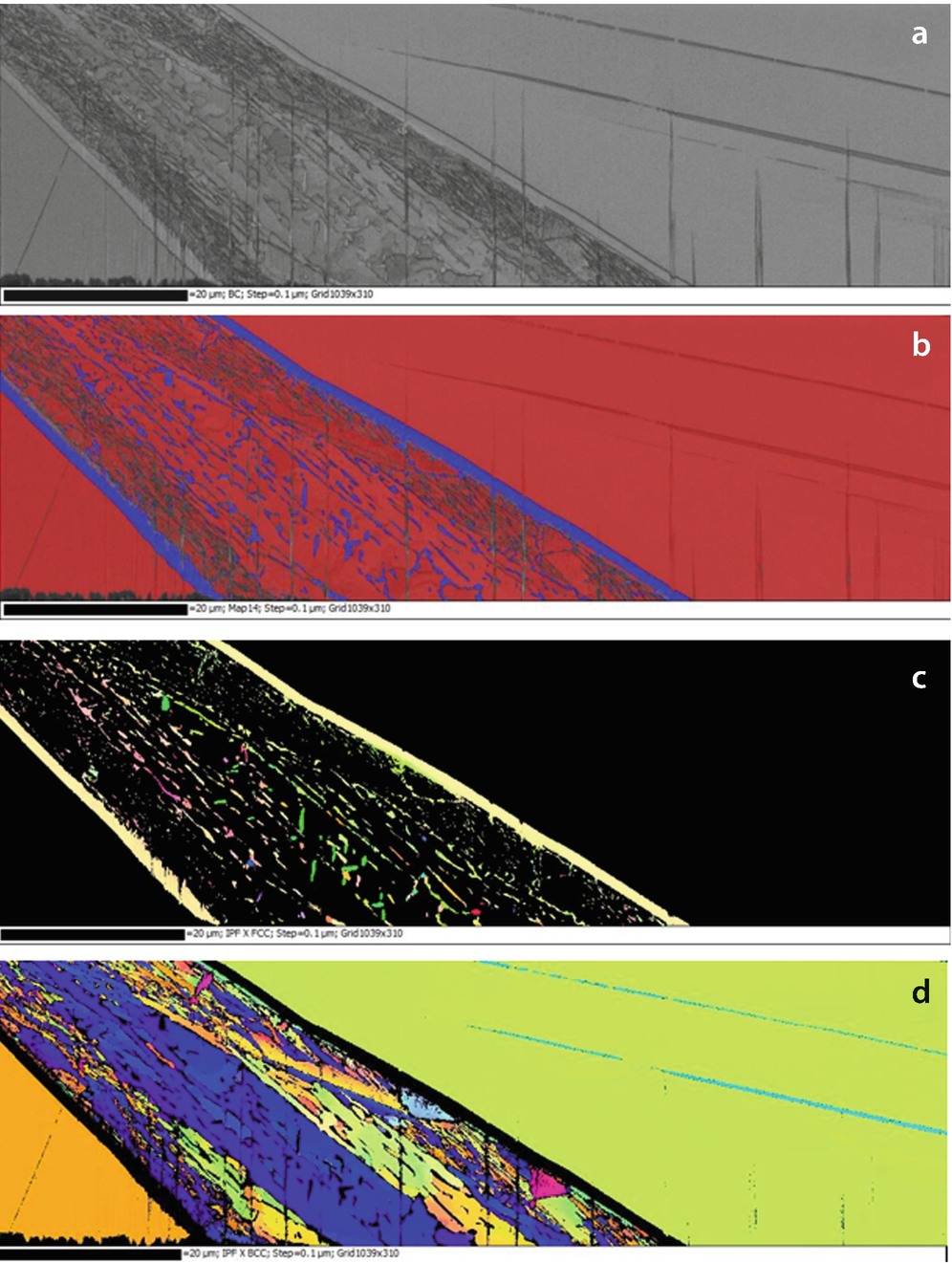
Fig. 30.13
EBSD results of the FIB prepared sample shown in ◘ Fig. 30.12. a Pattern contrast image demonstrates that the sample has little curtaining. b Phase map with ferrite (BCC) in red and Austenite (FCC) in blue. c Orientation map for the Austenite phase d Orientation map of the Ferrite phase (Bar = 20 µm)
This technique of sample lift-out is applicable to all imaging and analysis modes in the SEM. Once the sample is mounted flat on a surface or a support structure it is in an ideal sample orientation for imaging with secondary electrons of backscattered electrons. Lift-out samples also provide ideal sample orientations for EDS, WDS, or EBSD analysis. This is not true of cross sections that are milled into the bulk and not lifted out as access to the sample for some imaging and analysis techniques is not close to ideal depending on the particular FIB/SEM platform chosen (Giannuzzi 2006).
30.5.2 FIB Sample Preparation for 3D Techniques and Imaging
One of the truly important advances in FIB applications is the ability to automate the FIB operation and coordinate it with the SEM imaging or analysis using EDS or EBSD. This coordination allows the FIB column to be used to mill specified volumes from a sample face and then allow that same slice to be imaged or an analytical technique applied and then the process can be repeated. This is often referred to as serial sectioning. In this way a direct reconstruction (direct tomograph) of a 3D volume can be developed. One must always remember though that in this sort of work there is no ability to go back and start over unless a second suitable region is available. It is also important to remember the length scales that are practically reached with FIB methods. The typical area that can be accessed with LMIS-based FIB columns is 50 μm wide by 10 μm deep. The number of slices is limited by the operator’s patience and the stability of the FIB/SEM being utilized.
The first step is to deposit a protective layer over the entire region that is to be milled. This step is necessary, as discussed for single sections, to protect the sample region from damage by the ion beam. The larger the area to be sectioned, the larger the protective layer has to be and this deposition may be quite time consuming. Once the protective layer has been deposited, there are two ways to proceed with serial sectioning and imaging. The easiest method is to simply produce a cross section of the sample, as described previously. The polished face is then used as the starting point of the sectioning. One must be very careful when doing this to ensure that the trench that is cut is sufficiently wide to prevent the accumulation of redeposited material (material sputtered from the sample will often fill in the sides of the trench) from obscuring the region of interest. Once the initial trench has been prepared, the FIB/SEM can be set in automatic mode to proceed with the milling and imaging operations. This method is best used for imaging modes of operation (backscatter or secondary electron imaging) only as the access to the milled sample surface is limited. The resulting take-off angle for EDS in this mode is often sub-optimal, although good EDS spectrum imaging results have been obtained in this manner (Kotula et al. 2006).
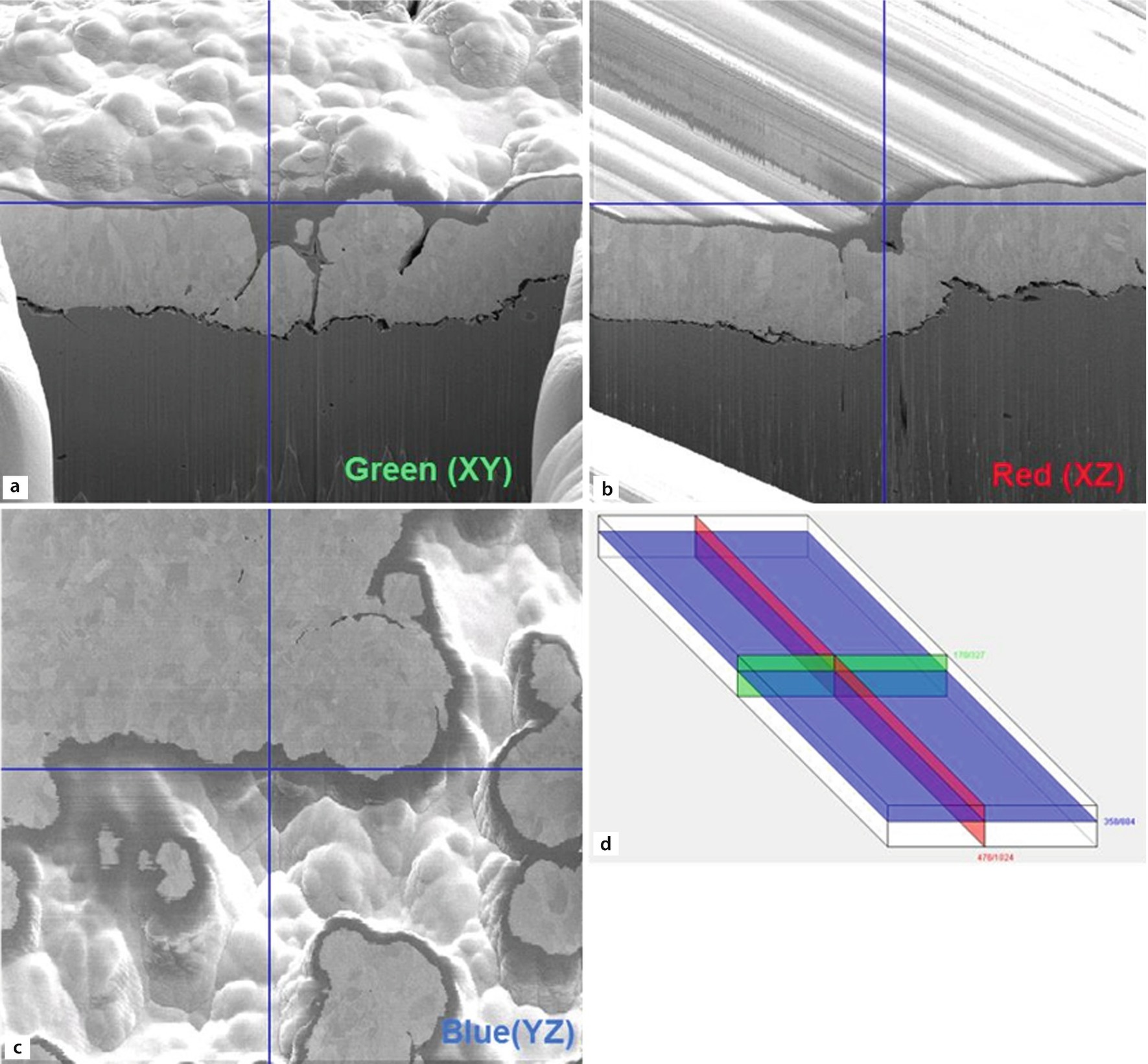
◘ Figure 30.14 is an example of the first method of serial sectioning where a volume of interest is imaged in the center of a sample. The sample is an electroplated coating on a substrate. The serial sectioning was accomplished by sequentially milling the exposed cross section followed by imaging with secondary electrons with the SEM column. ◘ Figure 30.14a contains examples of the “real” images obtained from the slicing and imaging process. The remaining images shown in ◘ Fig. 30.14b, c are obtained after the individual slices are aligned and stacked followed by the user selecting the planes of interest for image reconstruction.
Fig. 30.14
Image reconstruction of a plated stainless steel test coupon. Each section was milled perpendicular to the sample surface. These reconstructions were made from a series of 360 milled slices and required approximately 3 h to collect. The width of the milled area is 20 μm. a A secondary electron image of one milled cross section that is the green orientation shown in d. This image does not need to be reconstructed as it is the collected data. b Reconstructed slice along the red plane shown in d. This image is reconstructed once the slice thickness is known. The resolution in this direction is limited by the FIB milled slice thickness. c This is a reconstructed image of a slice parallel to the sample surface shown in blue in d. d Schematic of milled volume
A much faster method requires the volume of interest to be milled using any means into a cantilever-like beam that is then sliced starting at the free end. This method has numerous advantages over the bulk sample method as there is much easier access to the sample for imaging and analysis. This can also be accomplished by milling a chunk that contains the region of interest from the sample and then mounting the chunk onto a suitable support structure. The chunk then represents the cantilevered beam sample and is sequentially milled from the free side of the sample. This method is faster as much less material needs to be removed for each slice and there is no issue with re-deposition of the sputtered material. ◘ Figure 30.15 shows an example of the cantilever beam method for serial sectioning through a tin whisker on a copper substrate. In this case it was important to first protect the whisker with electron beam deposited platinum followed by ion beam deposited platinum. Once the feature of interest is protected from the ion beam, the material around the whisker is removed so that actual sectioning time during the serial sectioning will be minimized. EBSD orientation maps were collected at every slice during serial sectioning. Some commercially available FIB/SEMs require the sample to be repositioned for EBSD and then FIB slicing, while others possess a geometry where the sample does not have to be moved between sectioning and analytical acquisitions. For systems requiring movement between sectioning and EBSD, accurate alignment using fiducial marks is mandatory. ◘ Figure 30.16 is a reconstruction of the EBSD maps obtained from the tin whisker shown in ◘ Fig. 30.15. This data was acquired with a 200-nm slice thickness and an EBSD step size of 200 nm, leading to a voxel dimension of 200 × 200 × 200 nm. The acquisition required 75 sections that required a total time of 48 h to section and collect the EBSD data. Once this data is obtained and aligned and reconstructed then further examination of the spatial relationships between grains and the whisker are possible leading to an improved understanding of whisker growth.
Fig. 30.15
Preparation of a cantilever beam style sample for serial sectioning. a The sample before sectioning consist of the tin whisker coated extensively with platinum using first the electron beam and then the ion beam. The cantilever beam was shaped with the FIB and thinned to maximize the speed of cutting. b The same beam after serial sectioning. EBSD was performed at every slice. Note the large cross used as a fiducial to align images
Fig. 30.16
EBSD 3D reconstruction of a tin whisker from serial sectioning data in the FIB. The acquisition required 75 200-nm-thick sections and took nearly 48 h to complete sectioning and data acquisition
30.6 Summary
The combination of FIB and SEM is now an established and important technique for materials and biological sample preparation and has enable precise site specific samples to be produced. LMIS sources (mostly Ga) and plasma sources (mostly Xe) have been developed. The LMIS-equipped FIB tools produce much smaller probes that allow more precise sectioning due to a smaller probe size with higher current densities while the plasma FIB tools are finding application where large amounts of material need to be removed efficiently. The applications of FIB include sample preparation for imaging with electrons and ions and for a variety of analytical techniques including EBSD and EDS.
Open Access This chapter is licensed under the terms of the Creative Commons Attribution-NonCommercial 2.5 International License (http://creativecommons.org/licenses/by-nc/2.5/), which permits any noncommercial use, sharing, adaptation, distribution and reproduction in any medium or format, as long as you give appropriate credit to the original author(s) and the source, provide a link to the Creative Commons license and indicate if changes were made.
The images or other third party material in this chapter are included in the chapter's Creative Commons license, unless indicated otherwise in a credit line to the material. If material is not included in the chapter's Creative Commons license and your intended use is not permitted by statutory regulation or exceeds the permitted use, you will need to obtain permission directly from the copyright holder.