Electron beams have made possible the development of the versatile, high performance electron microscopes described in the earlier chapters of this book. Techniques for the generation and application of electron beams are now well documented and understood, and a wide variety of images and data can be produced using readily available instruments. While the scanning electron microscope (SEM) is the most widely used tool for high performance imaging and microanalysis, it is not the only option and may not even always be the best instrument to choose to solve a particular problem. In this chapter we will discuss how, by replacing the beam of electrons with a beam of ions, it is possible to produce a high performance microscope which resembles an SEM in many respects and shares some of its capabilities but which also offers additional and important modes of operation.
31.1 What Is So Useful About Ions?

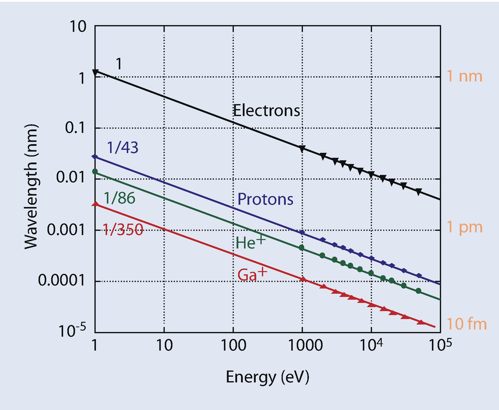
Comparison of wavelengths of various particles as a function of beam energy

a Gold islands on carbon as viewed by SEM and HIM under optimized conditions for each method: SEM (20-pA beam current at 1 keV); HIM (1-pA beam current at 30 keV). b High magnification HIM image of gold on carbon sample with lacey contamination visible. Field of View is 200 nm (Image acquired by Shawn McVey using the ORION Plus HIM) (Image courtesy of Carl Zeiss)
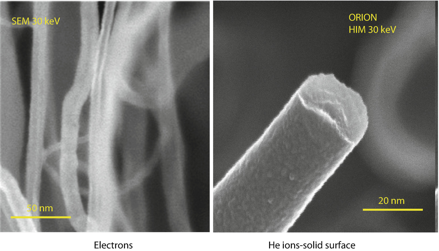
SEM and HIM images of soft material (polymer fibers)

a Image of two tungsten wires wetted by gallium. In this large field of view, the depth of field is over 800 μm, and all features are in focus. (Image acquired by Shawn McVey using the ORION NanoFab) (Image courtesy of Carl Zeiss) (Bar = 100 µm). b Illustration of the depth-of-field of helium ion microscopy at high resolution. The depth-of-field is at least 1.5 μm for an image width of 1 μm
High resolution helium ion imaging with high depth-of-field of a soft tissue sample, human pancreatic cells (Sample courtesy of Paul Walther, Univ. of Ulm)
All electrons are the same—but all ions are not, and so many different ion-based microscopes can be configured and optimized for the various tasks. At present the most widely used ion beam for high resolution imaging is helium (He+), while gallium (Ga+) is widely used for ion beam machining of materials. Historically the earliest ion beam microscope (Levi-Setti 1974) used protons (H+), while more recently argon (Ar+), neon (Ne+), and lithium (Li+) beams have all also been put into use for nanoscale imaging and fabrication. At present negatively charged ions are much less widely employed than the corresponding positive species, but it can be safely anticipated that they will eventually be employed for special purposes because of the additional versatility that they can offer.
Although in principle any ion could be employed for microscopy, using a heavier ion requires a correspondingly higher accelerating voltage to operate than does a lighter ion, and this heavy ion bombardment may cause significantly more damage to the specimen under examination. Heavy ions also usually have multiple ionization states and these may result in emitted beams whose incident energy is effectively distributed across several values spanning a wide range. This energy spread, in turn, may result in chromatic aberrations in the lenses which may then further degrade the achievable resolution.
In addition, while all energetic ions cause sputtering of the target atoms to some degree and also implant into the target, which can locally alter the target composition, ions of higher mass, such as Ga+ and above, have higher sputtering rates that may substantially alter the target. While acceptable for some tasks such as thinning or machining materials, the level of damage per incident heavy ion is undesirable for imaging purposes because such significant local alteration occurs that the fine spatial details of the specimen are lost before an image representative of the original material can be successfully captured.
31.2 Generating Ion Beams
The approach now most commonly employed for producing a beam of ions for use in microscopy is a development of the method originally employed by Prof. Erwin Muller at Penn State University in the 1940s and 1950s (Muller 1965). Muller’s device was a sealed metal cylinder containing helium gas which was cooled to a temperature of just a few degrees Kelvin (K). At one end of the cylinder was a sharply pointed metal needle connected to a power supply capable of supporting a positive voltage of up to a few kilovolts, while at the other end was a fluorescent imaging screen. When neutral helium atoms drifted towards the needle they became ionized due to the high electric field gradient and acquired a positive potential which then resulted in them being accelerated away from the tip and towards the viewing screen where they formed into an image. On October 11, 1955, Muller and his students were able to demonstrate for the first time ever the direct observation of an atomic structure. Almost 20 years later Professor Riccardo Levi-Setti of the University of Chicago developed a modification of Muller’s ion source which allowed it to generate ion beams that could be focused, scanned, and used for imaging in the same way as electrons in a conventional SEM (Levi-Setti 1974). It was this development that became the basis for the source for the present helium ion microscope (HIM).
In present-day ion beam microscopes, the emitter is once again fabricated into the form of a needle, but now the exact size and shape of this tip is very carefully optimized. Using patented, and proprietary, procedures developed by the Zeiss company the emitter tip is shaped and sharpened until it contains just three atoms (Notte et al. 2006). This “trimer” configuration is inherently more stable than any more random arrangement and also ensures that the maximum emitted ion current is directed parallel to the axis of the ion beam. A carefully placed, moveable aperture can then be used to select any one of the three “trimer” ion emission peaks to be used as the beam source for the instrument. The available ion beam current varies with the magnitude of the helium, or other gas, pressure and can reach values as high of several hundred picoamperes.
Low energy ions, i.e., those with less than about 1 MeV of energy, are not significantly affected by magnetic fields so all of the lenses must be electrostatic in type rather than magnetic. The ion beam then travels along the microscope column until it reaches the specimen where its interaction generates ion-induced secondary electrons (iSE) as well as, in some cases, other signals. The ion emitter is adequately stable and provides a bright signal for periods from 5–10 h before the emitter needs to be re-optimized. Once the available beam current becomes too low in intensity, or too unstable to be useful, then the tip must be reformed. This can be done in situ by the operator using an automated procedure which takes some 10–20 min to complete.
Changing from the familiar He+ beam to a Ne+ beam, or to some other source of emission, requires that any residual gas in the chamber must be first pumped away. The desired new gas of choice can then be injected into the chamber, and the system can be brought back into operation by reforming the “trimer” as described earlier. The usable overall lifetime of these emitters is typically of the order of many months when they are treated with reasonable care and attention.
Although in many ways operating a helium ion beam (HIM) microscope is similar to operating a conventional SEM, to fully optimize the performance of the HIM it is necessary to pay more attention to certain details. The ion source offers just two adjustable controls—the “extractor” which determines the field at the tip and so controls the emission of the source, and the “accelerator” which determines the landing energy of the beam on to the specimen surface. The extractor module “floats” on the top of the potential determined by the accelerator setting, and both the brightness and the stability of the ion source are affected by the extractor module settings. As the extractor potential is increased, the emission current rises before reaching a plateau at the so-called “best imaging voltage” (BIV), which for helium ions occurs at a field strength of about 44 V/nm depending on the geometry of the tip itself. Exceeding the BIV will make the beam less stable, and can result in so much damage to the emitter that it may become necessary to reform the tip again before reliable operation can be restored. The “accelerator” control determines the actual landing energy of the ions on the specimen. For a He+ beam this energy is usually in the range 25–45 keV while for a heavier ion such as Ne+ the corresponding value is more typically in the 20–35-keV range. In either case the yield of secondary electrons increases with the accelerator setting, but continuous operation with the system at energies of 45 keV or higher may cause problems such as insulator breakdowns and discharges. It is therefore good practice to record and save all the experimental parameters likely to be encountered.
31.3 Signal Generation in the HIM

Monte Carlo ion beam trajectory simulations for various ion species. E 0 = 40 keV

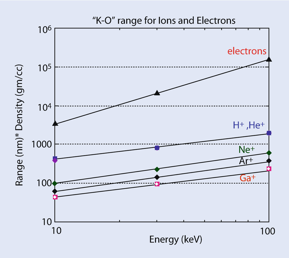
Plot of Kanaya–Okayama range for electrons and various ion species


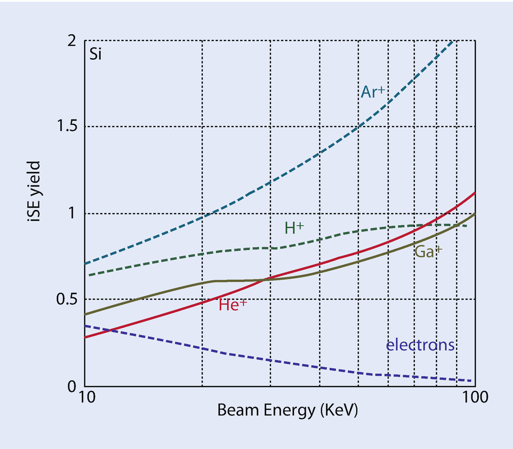
Yield of secondary electrons from Si for electrons and various ions as a function of energy
31.4 Current Generation and Data Collection in the HIM
A typical ion beam microscope operates at energies selected between 10 and 35 keV, and generates an incident beam current of the order of 0.1 pA to >100 pA at the specimen. These ions interact with the specimen of interest generating an iSE secondary electron signal which can be collected by an Everhart–Thornley (ET) detector very similar to that used in the conventional SEM. The signal is then passed through an “analog to digital” (A/D) convertor for real-time display and for storage. Because the incident ion beam currents are quite low, the A/D convertor, which samples the incoming iSE signal at a fixed repetition period of 100 ns, will likely completely miss many of these sparsely generated signal pulses. To overcome this problem, an additional image control labeled as “image intensity” (II) has been added to the familiar SEM brightness and contrast controls. This “image intensity” control allows the operator to choose between (a) the true averaging mode in which N successive A/D conversions are made and the total yield is then divided by N and (b) the true integration mode in which N successive A/D conversions are summed and that value is then reported, or any arbitrary setting between these two extremes. (J. Notte 2015, personal communication). The addition of this illumination control provides considerable additional imaging flexibility while ensuring that the usual “brightness” and “contrast” controls are still able to determine the overall appearance of the image.
High spatial resolution and high depth of field HIM imaging of Ga-ion-beam etched Al-Cu aligned eutectic alloy. Vertical relief approximately 5 µm. (Bar = 1 µm) (A. Vladar and D. Newbury, NIST)
The strategy for operating the HIM is different than that of a conventional SEM because the incident beam energy is generally held fixed at the highest possible energy, typically in the range 30–40 keV, because this simultaneously optimizes both the signal-to-noise ratio and the image resolution. When there is a requirement to examine sub-surface detail this can best be achieved by exploiting the inevitable removal of surface layers by the ion beam as it “rasters” across the sample. Material can then be removed at the rate of a few tens of nanometers per minute, with images stored every few seconds to yield a full three-dimensional reconstruction of the sampled volume.
Charging is an inevitable problem for the HIM. The high SE coefficient of ion beams tends to cause positive charging at the surface, which is further exacerbated by the positive charge injected by the positive He+ ions. The simplest and most reliable technique to control such positive charging is to periodically flood the specimen surface with a very low energy electron beam so as to re-establish charge balance before starting the next scan, although this approach requires care to eliminate both under- and over-compensation. An alternative approach is to inject air into the specimen chamber through a small jet positioned just a short distance away from the desired sample region. This is easy to implement and requires little supervision once an initial charge balance has been achieved.
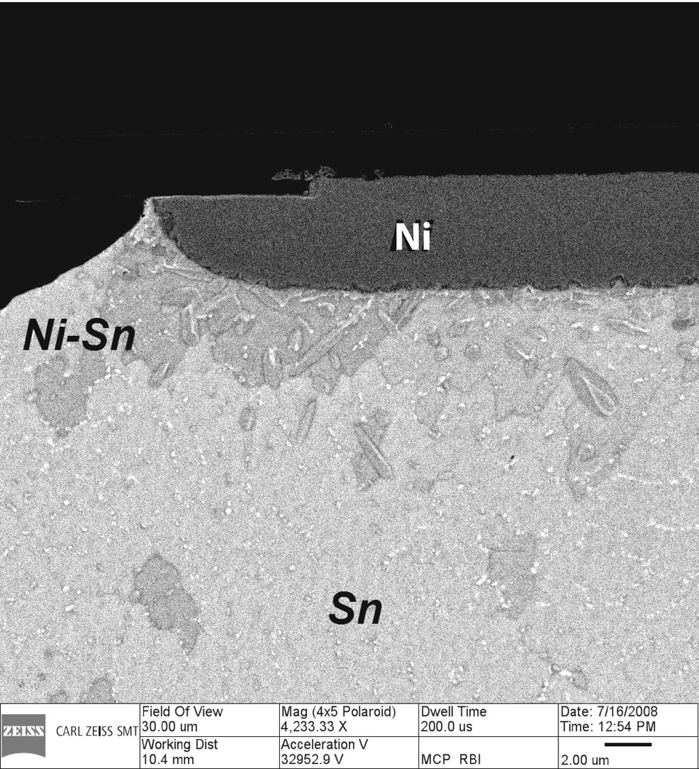
Reaction zone at Sn-Ni interface as imaged with ORION Plus HIM from backscattered helium striking the annular microchannel plate. Field of view is 30 μm. Material composition is easily distinguished by atomic number contrast (Bar = 2 µm) (Sample provided by F. Altmann of the Fraunhofer Institute for Mechanics of Materials, Halle, Germany; Image courtesy of Carl Zeiss)
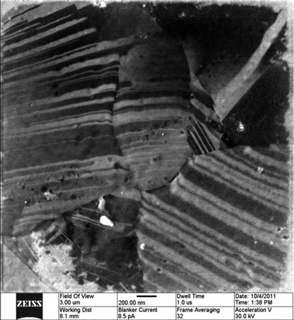
Ion channeling contrast observed in deposited copper showing the distinct crystal grains. The field of view is 3 μm, and the incident beam was helium at E 0 = 30 keV (Bar = 200 nm) (Imaged with the E–T detector using the ORION Plus, courtesy of Carl Zeiss)
31.5 Patterning with Ion Beams
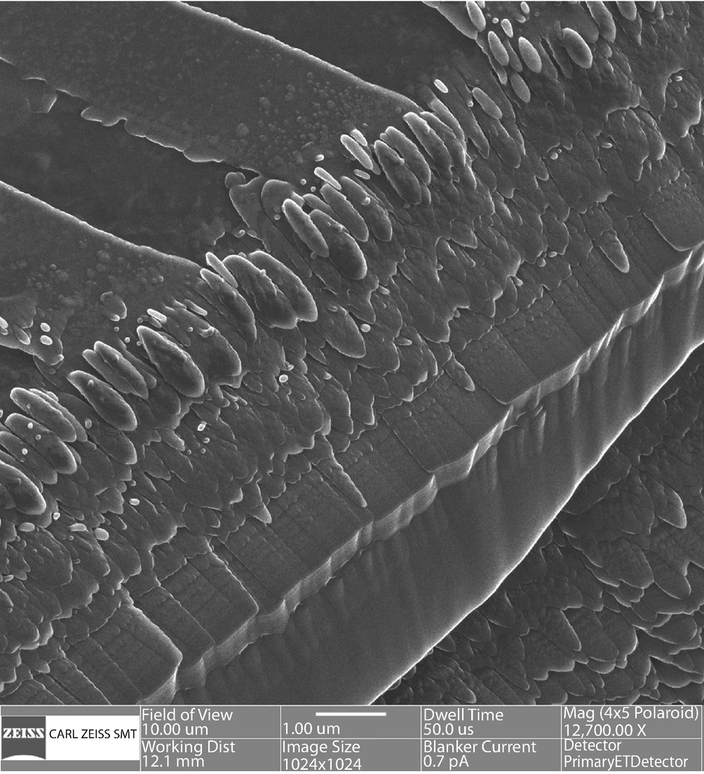
When ions strike a target they always remove a finite amount of material from the top surface by the process called “sputtering,” which involves ion-atom collisions that dislodge atoms and transfer sufficient kinetic energy so that a small fraction escape the sample. While this is sometimes a problem when imaging is the main application of a microscope, the ability of ion beams to remove material in a controlled fashion from a surface is of considerable and increasing value. At its simplest this capability can be applied to generate simple structures such as arrays of holes, or to pattern substrates. The typical beam choice for this process is gallium because of its high sputtering coefficient, but residual gallium becomes embedded in the material being machined. Neon is also a useful candidate for the gas as it can remove material at about 60 % of the speed of gallium but without permanently depositing anything into the target material. For the very softest or most fragile materials a helium ion beam can also pattern at a slow but acceptable rate.
An important current use of this technology relies on “Graphene” as the material of choice. Graphene comes in the form of flexible sheets which may be only by a few atom layers in thickness and yet can readily be cut and shaped as required. Graphene provides the basis to fabricate nanoscale semiconductor devices, and varieties of other active structures.
31.6 Operating the HIM
Using a He+, or some other, ion beam for imaging materials is somewhat different from, although not really much more complex than, conventional imaging with electrons. However some planning prior to turning on the ion beam will help by minimizing beam damage optimizing conditions, and improving specimen throughput.
Step 1
Choose the initial ion beam to be employed. If only one beam type is available, for example, Ga+, then this step is not crucial because it should imply that the required operating choices have already been optimized. However, if several different ion beam species are available then a planned strategy becomes necessary. If there is only a limited amount of the sample then the user should start with the softest ion beam available—helium—so as to minimize damage in the near-surface region of the specimen—and image as required. Only when this set of images is completed should a more aggressive beam choice be tried.
Step 2
Select the desired beam energy. The best choice is always the highest voltage available because this will enhance image resolution, and the ion source will be running at its optimum efficiency. Even at modestly high energies, for example 45 keV, the depth of penetration of ions into most specimens will generally be less than that of a conventional SEM operating at just a few hundred electron volts. If the signal-to-noise of the image appears to be good enough to record useful information then it is worth trying to reduce the incident beam current by using a smaller beam current in the column to see if the damage rate of the sample can be reduced while simultaneously increasing the imaging depth of field.
Step 3
Next choose a working distance (WD) from the source to the sample. Obtaining the shortest possible WD is not as important in an ion microscope as it is in a conventional SEM because the aberrations of the ion beam-optical system are much less severe than those in conventional electron optics. Using a longer working distance will allow safer specimen tilting and manipulation. Before proceeding also ensure that the specimen stage and its specimens are not touching anything else, nor obscuring access to the various detectors, probes, and accessories in the column and chamber.
Step 4
If these are the first observations of the sample which is now in the HIM, then try recording images from some expendable region of the specimen at several different magnifications and currents to confirm whether or not ion-induced beam damage is going to be a problem. In any case always start imaging at the lowest possible magnification and work up from there. Working “high to low” is likely to be unsatisfactory because the damage induced at higher magnification will be obvious as the magnification is reduced. Also check the imaged field of view from time to time for signs of damage, or any indications of drift.
Step 5
Maintain a constant check on the incident ion beam current. If this is falling, or if the images are becoming noisy and unstable, then the emitter tip should be reformed before continuing.
31.7 Chemical Microanalysis with Ion Beams
The ability of a microscope to image a material while simultaneously performing a chemical microanalysis of the material is of great value in all areas of science and technology. As a result a high percentage of all SEMs are equipped with X-ray detectors for the identification and analysis of specimen composition. However, X-ray generation is only possible when the velocity of the incoming charged particle (electrons or ions) equals or exceeds the velocity of the orbiting electron within the sample. For an incident beam of electrons these two energies will only be numerically equal in value when their velocities are the same. When the kinetic energy of a beam electron matches the ionization (binding) energy of an atomic shell electron, inelastic scattering of the beam electron becomes possible, causing ejection of that atomic electron. But when the incident beam is made of helium ions, which have a mass 7300 times heavier than an electron, then the energy of the ion also has to be increased by a factor of 7300× by accelerating it before atomic ionization becomes possible. X-ray microanalysis with an ion beam is therefore only possible with ion beam energies in the MeV range, which is far above the operating energy of the HIM.
Possibly the most promising approach for chemical analysis using ion beams at present is Time of Flight- Secondary Ion Mass Spectrometry (TOF-SIMS), which directly analyzes the specimen atoms sputtered atoms from the surface by the primary ion beam. In this method the specimen of interest is contained in the sample chamber in the usual way, but on one side of the chamber is a shutter which can be opened or closed at very high speed as required. The ion beam is then switched on for a short period of time, striking the specimen and sputtering the top two or three atomic layers of the specimen, including neutral, negative, and positive fragments and at the same time the shutter is opened. Which fragment of the sample, positive or negative, is to be analyzed is determined by the polarity of the electric field applied in the chamber. The chosen charged particles from the sample drift toward the shutter at which point they are abruptly accelerated by a strong electric field and travel on until they reach the detector which records the time taken from the original electrical pulse. This time interval will depend on the mass as well as the charge of the particle and so by measuring the transit time required to reach the detector, the mass-to-charge ratio of each individual atom cluster can be deduced. Given accurate “time of transit” measurement capability on the system, this mass-to-charge ratio data can provide rapid, reliable, and unique identification of all the atomic and cluster ions ejected during ion bombardment. After a suitable time interval the shutter is again closed, the system is briefly allowed to stabilize, and the operation is then repeated as often as required to achieve adequate statistics.
TOF-SIMS offers some significant advantages over other possible approaches. The incident ion beam can either be held stationary at a point, or scanned across a chosen area as required to produce a chemical map. Each cycle of this process will then physically remove a few atomic layers from the analyzed area, so repeated measurements on the same area can eventually provide a three-dimensional view of the sampled region. Most important of all, this approach to analysis provides detailed information about the actual chemistry of the area selected, identifying the chemistry of the various compounds, clusters, and elements that are present whereas conventional X-ray microanalysis can only identify which elements are present. This technology is presently only available on a few dual-beam Ga+ “focused ion beam source” (SEM–FIB) instruments, but many groups are now working to extend this capability to the HIM.

Open Access This chapter is licensed under the terms of the Creative Commons Attribution-NonCommercial 2.5 International License (http://creativecommons.org/licenses/by-nc/2.5/), which permits any noncommercial use, sharing, adaptation, distribution and reproduction in any medium or format, as long as you give appropriate credit to the original author(s) and the source, provide a link to the Creative Commons license and indicate if changes were made.
The images or other third party material in this chapter are included in the chapter's Creative Commons license, unless indicated otherwise in a credit line to the material. If material is not included in the chapter's Creative Commons license and your intended use is not permitted by statutory regulation or exceeds the permitted use, you will need to obtain permission directly from the copyright holder.