© Springer Science+Business Media LLC 2018
Joseph I. Goldstein, Dale E. Newbury, Joseph R. Michael, Nicholas W.M. Ritchie, John Henry J. Scott and David C. JoyScanning Electron Microscopy and X-Ray Microanalysishttps://doi.org/10.1007/978-1-4939-6676-9_7

7. SEM Image Interpretation

Joseph I. Goldstein1 , Dale E. Newbury2, Joseph R. Michael3, Nicholas W. M. Ritchie2, John Henry J. Scott2 and David C. Joy4
(1)
University of Massachusetts, Amherst, Massachusetts, USA
(2)
National Institute of Standards and Technology, Gaithersburg, Maryland, USA
(3)
Sandia National Laboratories, Albuquerque, New Mexico, USA
(4)
University of Tennessee, Knoxville, Tennessee, USA
 

7.1 Information in SEM Images

Information in SEM images about specimen properties is conveyed when contrast in the backscattered and/or secondary electron signals is created by differences in the interaction of the beam electrons between a specimen feature and its surroundings. The resulting differences in the backscattered and secondary electron signals (S) convey information about specimen properties through a variety of contrast mechanisms. Contrast (C tr) is defined as

$$ {C}_{tr}=\left({S}_{\mathrm{max}}-{S}_{\mathrm{min}}\right)/{S}_{\mathrm{max}} $$
(7.1)
where is S max is the larger of the signals. By this definition, 0 ≤ C tr ≤ 1.
Contrast can be conveyed in the signal by one or more of three different mechanisms:
  1. 1.

    Number effects. Number effects refer to contrast which arises as a result of different numbers of electrons leaving the specimen at different beam locations in response to changes in the specimen characteristics at those locations.

     
  2. 2.

    Trajectory effects. Trajectory effects refer to contrast resulting from differences in the paths the electrons travel after leaving the specimen.

     
  3. 3.

    Energy effects. Energy effects occur when the contrast is carried by a certain portion of the backscattered electron or secondary electron energy distribution. For example, the high-energy backscattered electrons are generally the most useful for imaging the specimen using contrast mechanisms such as atomic number contrast or crystallographic contrast. Low-energy secondary electrons are likely to escape from a shallow surface region of a specimen and convey surface information.


7.2 Interpretation of SEM Images of Compositional Microstructure

7.2.1 Atomic Number Contrast With Backscattered Electrons

The monotonic dependence of electron backscattering upon atomic number (η vs. Z, shown in ◘ Fig. 2.​3) constitutes a number effect with predictable behavior that enables SEM imaging to reveal the compositional microstructure of a specimen through the contrast mechanism variously known as “atomic number contrast,” “compositional contrast,” “material contrast,” or “Z-contrast.” Ideally, to observe unobscured atomic number contrast, the specimen should be flat so that topography does not independently modify electron backscattering. An example of atomic number contrast observed in a polished cross section of Raney nickel alloy using signal collected with a semiconductor backscattered electron (BSE) detector is shown in ◘ Fig. 7.1, where four regions with progressively higher gray levels can be identified. The systematic behavior of η versus Z allows the observer to confidently conclude that the average atomic number of these four regions increases as the average gray level increases. SEM/EDS microanalysis of these regions presented in ◘ Table 7.1 gives the compositional results and calculated average atomic number, Z av, of each phase. The Z av values correspond to the trend of the gray levels of the phases observed in ◘ Fig. 7.1.
../images/271173_4_En_7_Chapter/271173_4_En_7_Fig1_HTML.jpg
Fig. 7.1

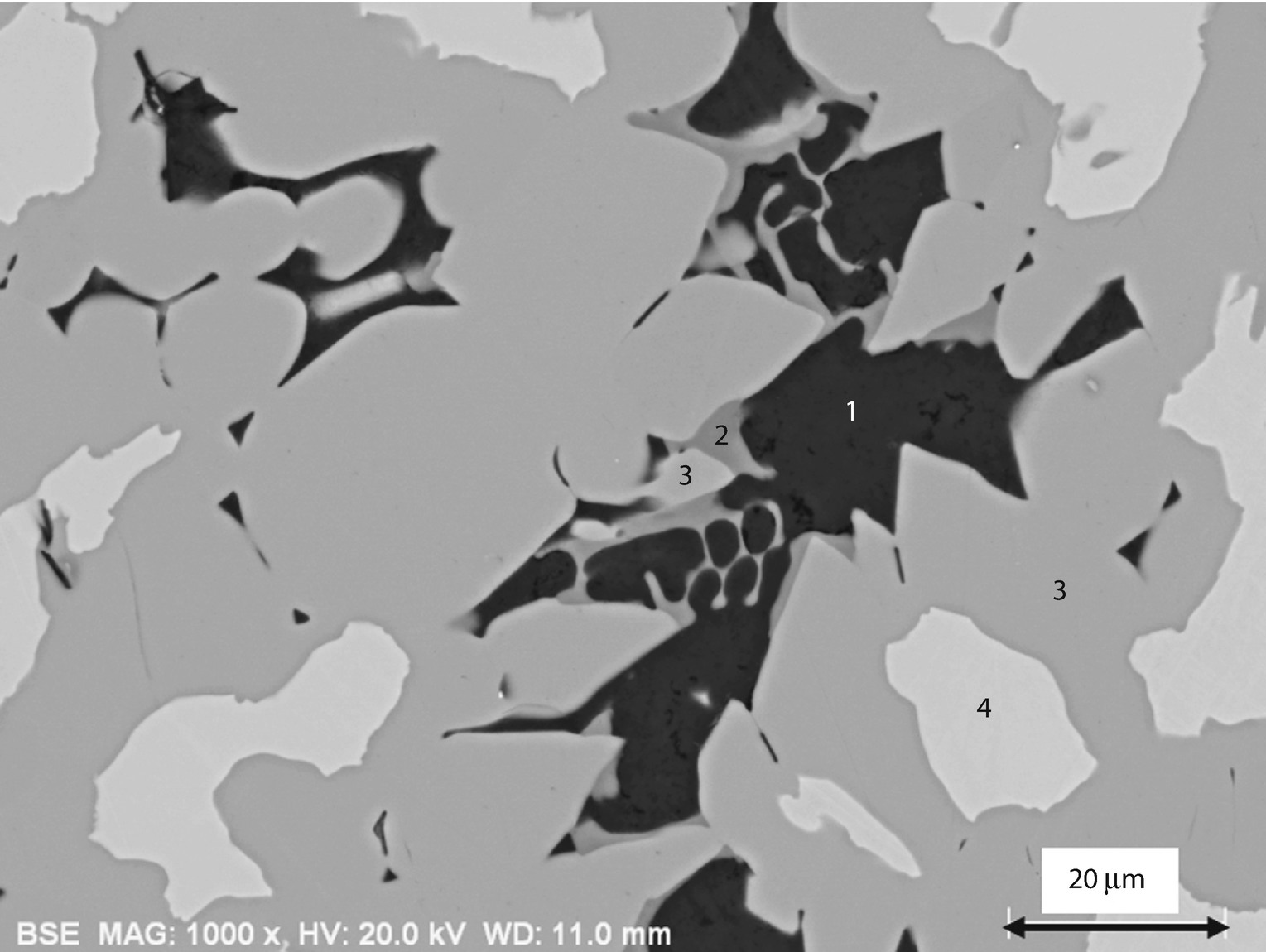
Raney nickel; E 0 = 20 keV; semiconductor BSE detector (SUM mode)

Table 7.1

Raney nickel alloy (measured composition, calculated average atomic number, backscatter coefficient, and atomic number contrast across the boundary between adjacent phases)

Phase

Al (mass frac)

Fe (mass frac)

Ni (mass frac)

Z av

Calculated, η

Contrast

1

0.9874

0.0003

0.0123

13.2

0.155


2

0.6824

0.0409

0.2768

17.7

0.204

1–2 0.24

3

0.5817

0.0026

0.4155

19.3

0.22

2–3 0.073

4

0.4192

0.0007

0.5801

21.7

0.243

3–4 0.095

7.2.2 Calculating Atomic Number Contrast

An SEM is typically equipped with a “dedicated backscattered electron detector” (e.g., semiconductor or passive scintillator) that produces a signal, S, proportional to the number of BSEs that strike it and thus to the backscattered electron coefficient, η, of the specimen. Note that other factors, such as the energy distribution of the BSEs, can also influence the detector response.

If the detector responded only to the number of BSEs, the contrast C tr, can be estimated as

$$ {C}_{\mathrm{tr}}=\left({S}_{\mathrm{max}}-{S}_{\mathrm{min}}\right)/{S}_{\mathrm{max}}=\left({h}_{\mathrm{max}}-{h}_{\mathrm{min}}\right)/{h}_{\mathrm{max}} $$
(7.2)
Values of the backscatter coefficient for E 0 ≥ 10 keV can be conveniently estimated using the fit to η versus Z (Eq. 2.​2). Note that for mixtures that are uniform at the atomic level (e.g., alloy solid solutions, compounds, glasses, etc.), the backscattered electron coefficient can be calculated from the mass fraction average of the atomic number inserted into Eq. 2.​2 (as illustrated for the Al-Fe-Ni phases listed in ◘ Table 7.1), or alternatively, from the mass fraction average of the pure element backscatter coefficients.
The greater the difference in atomic number between two materials, the greater is the atomic number contrast. Consider two elements with a significant difference in atomic number, for example, Al (Z = 13, η = 0.152) and Cu (Z = 29, η = 0.302). From Eq. (7.1), the atomic number contrast between Al and Cu is estimated to be

$$ {\displaystyle \begin{array}{c}{C}_{tr}=\left({h}_{\mathrm{max}}-{h}_{\mathrm{min}}\right)/{h}_{\mathrm{max}}\\ {}=\left(0.302-0.152\right)/0.302=0.497\end{array}} $$
(7.3)
When the contrast is calculated between elements separated by one unit of atomic number, much lower values are found, which has an important consequence on establishing visibility, as discussed below. Note that the slope of η versus Z decreases as Z increases, so that the contrast (which is the slope of η vs. Z) between adjacent elements (ΔZ = 1) also decreases. For example, the contrast between Al (Z = 13, η = 0.152) and Si (Z = 14, η = 0.164) where the slope of η versus Z is relatively high is

$$ {\displaystyle \begin{array}{c}{C}_{\mathrm{tr}}=\left({h}_{\mathrm{max}}-{h}_{\mathrm{min}}\right)/{h}_{\mathrm{max}}\\ {}=\left(0.164-0.152\right)/0.164=0.073\end{array}} $$
(7.4)
A similar calculation for Cu (Z = 29, η = 0.302) and Zn (Z = 30, η = 0.310) where the slope of η versus Z is lower gives

$$ {C}_{\mathrm{tr}}=\left(0.310-0.302\right)/0.310=0.026 $$
(7.5)
For high atomic number elements, the slope of η versus Z approaches zero, so that a calculation for Pt (Z = 78, η = 0.484) and Au (Z = 79, η = 0.487) gives a very low contrast:

$$ {C}_{\mathrm{tr}}=\left(0.487-0.484\right)/0.487=0.0062 $$
(7.6)
◘ Figure 7.2 summarizes this behavior in a plot of the BSE atomic number contrast for a unit change in Z as a function of Z.
../images/271173_4_En_7_Chapter/271173_4_En_7_Fig2_HTML.png
Fig. 7.2

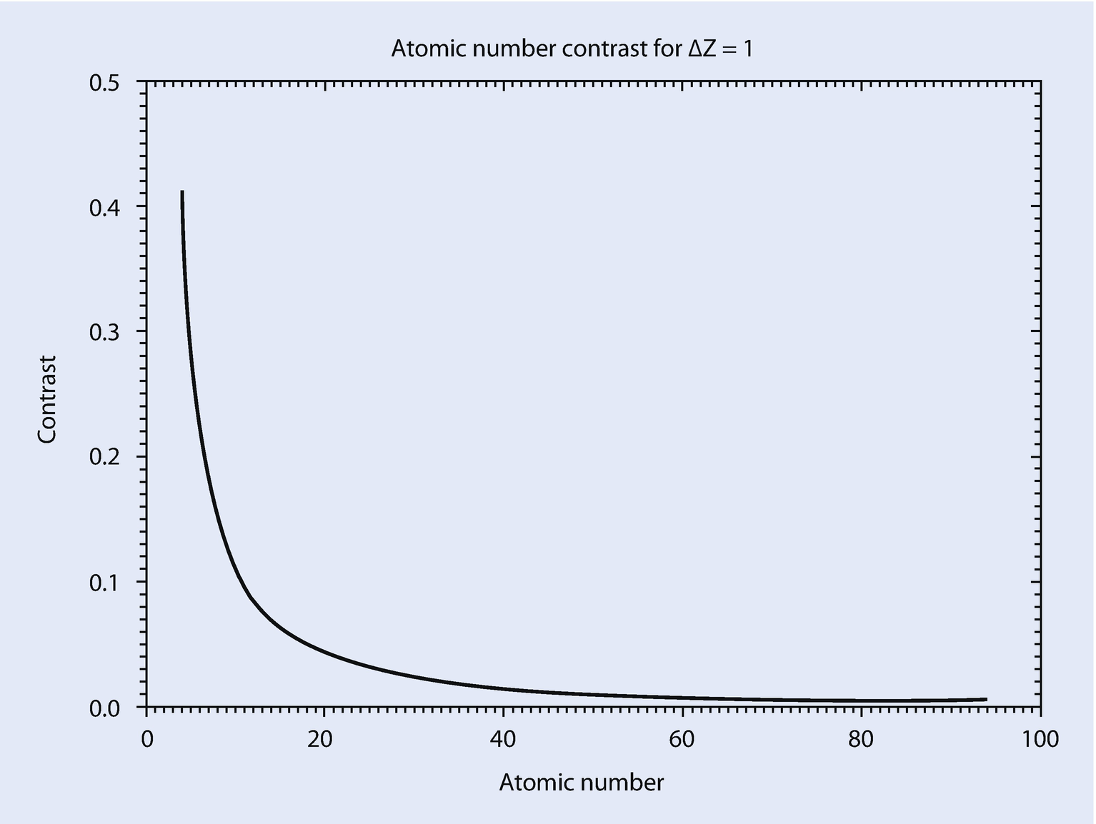
Atomic number contrast for pure elements with ΔZ = 1

7.2.3 BSE Atomic Number Contrast With the Everhart–Thornley Detector

The appearance of atomic number contrast for a polished cross section of Al-Cu aligned eutectic, which consists of an Al-2 % Cu solid solution and the intermetallic CuAl2, is shown as viewed with a semiconductor BSE detector in ◘ Fig. 7.3a and an Everhart–Thornley detector (positively biased) in ◘ Fig. 7.3b. The E–T detector is usually thought of as a secondary electron detector, and while it captures the SE1 signal, it also captures BSEs that are directly emitted into the solid angle defined by the scintillator. Additionally, BSEs are also represented in the E–T detector signal by the large contribution of SE2 and SE3, which are actually BSE-modulated signals. Thus, although the SE1 signal of the E–T detector does not show predictable variation with composition, the BSE components of the E–T signal reveal the atomic number contrast seen in ◘ Fig. 7.3b. It must be noted, however, that because of the sensitivity of the E–T detector to edge effects and topography, these fine-scale features are much more visible in ◘ Fig. 7.3b than in ◘ Fig. 7.3a.
../images/271173_4_En_7_Chapter/271173_4_En_7_Fig3_HTML.png
Fig. 7.3

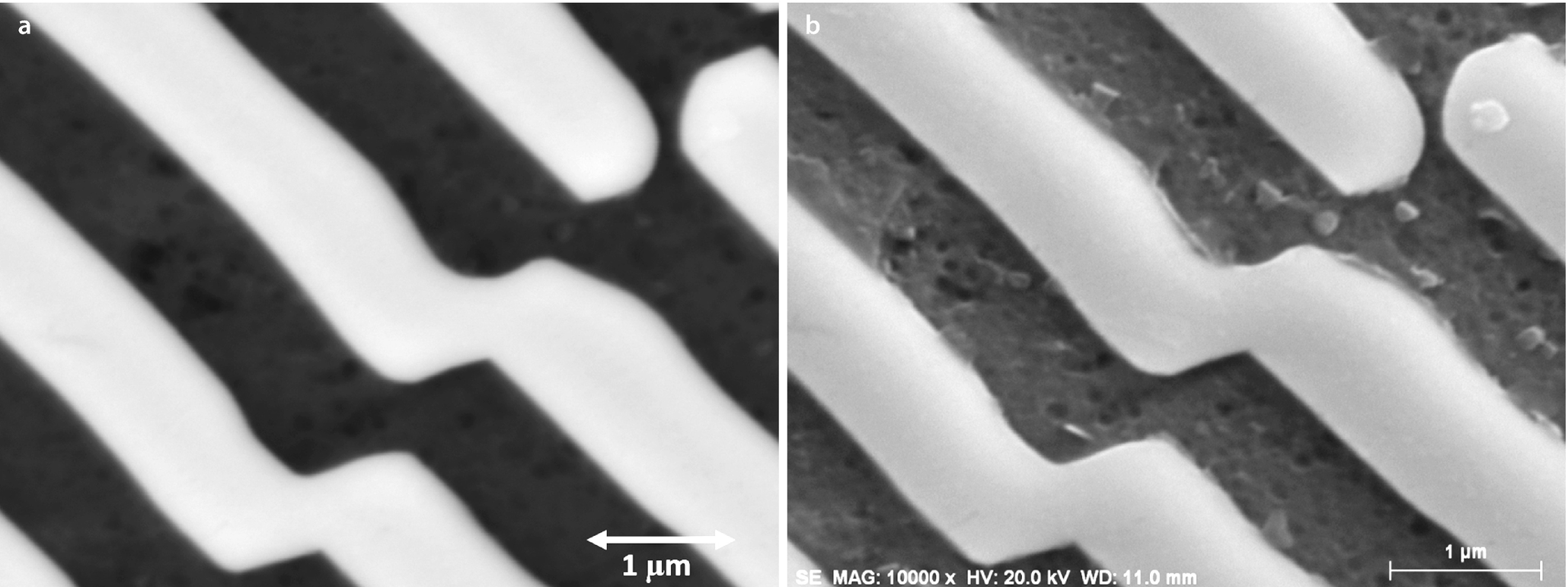
Aligned Al-Cu eutectic; E 0 = 20 keV: a semiconductor BSE detector (SUM mode); b Everhart–Thornley detector (positive bias)

For both the dedicated semiconductor BSE detector and the E–T detector, the higher atomic number regions appear brighter than the lower atomic number regions, as independently confirmed by energy dispersive X-ray spectrometry of both materials. However, the semiconductor BSE detector actually enhances the atomic number contrast over that estimated from the composition (Al-0.02Cu, η = 0.155; CuAl2, η = 0.232, which gives C tr = 0.33). The semiconductor detector shows increased response from higher energy backscattered electrons, which are produced in greater relative abundance from Cu compared to Al, thus enhancing the difference in the measured signals. The response of the Everhart-Thornley detector (positive bias) to BSEs is more complex. The BSEs that directly strike the scintillator produce a greater response with increasing energy. However, this component is small compared to the BSEs that strike the objective lens pole piece and chamber walls, where they are converted to SE3 and subsequently collected. For these remote BSEs, the lower energy fraction actually create SEs more efficiently.

7.3 Interpretation of SEM Images of Specimen Topography

Imaging the topographic features of specimens is one of the most important applications of the SEM, enabling the microscopist to gain information on size and shape of features. Topographic contrast has several components arising from both backscattered electrons and secondary electrons:
  1. 1.

    The backscattered electron coefficient shows a strong dependence on the surface inclination, η versus θ. This effect contributes a number component to the observed contrast.

     
  2. 2.

    Backscattering from a surface perpendicular to the beam (i.e., 0° tilt) is directional and follows a cosine distribution η(φ) ≈ cos φ (where φ is an angle measured from the surface normal) that is rotationally symmetric around the beam. This effect contributes a trajectory component of contrast.

     
  3. 3.

    Backscattering from a surface tilted to an angle θ becomes more highly directional and asymmetrical as θ increases, tending to peak in the forward scattering direction. This effect contributes a trajectory component of contrast.

     
  4. 4.

    The secondary electron coefficient δ is strongly dependent on the surface inclination, δ(θ) ≈ sec θ, increasing rapidly as the beam approaches grazing incidence. This effect contributes a number component of contrast.

     
Imaging of topography should be regarded as qualitative in nature because the details of the image such as shading depend not only on the specimen characteristics but also upon the response of the particular electron detector as well as its location and solid angle of acceptance. Nevertheless, the interpretation of all SEM images of topography is based on two principles regardless of the detector being used:
  1. 1.

    Observer’s Point-of-View: The microscopist views the specimen features as if looking along the electron beam.

     
  2. 2.
    Apparent Illumination of the Scene:
    1. a.

      The apparent major source of lighting of the scene comes from the position of the electron detector.

       
    2. b.

      Depending on the detector used, there may appear to be minor illumination sources coming from other directions.


7.3.1 Imaging Specimen Topography With the Everhart–Thornley Detector

SEM images of specimen topography collected with the Everhart–Thornley (positive bias) detector (Everhart and Thornley 1960) are surprisingly easy to interpret, considering how drastically the imaging technique differs from ordinary human visual experience: A finely focused electron beam steps sequentially through a series of locations on the specimen and a mixture of the backscattered electron and secondary electron signals, subject to the four number and trajectory effects noted above that result from complex beam–specimen interactions, is used to create the gray-scale image on the display. Nevertheless, a completely untrained observer (even a young child) can be reasonably expected to intuitively understand the general shape of a three-dimensional object from the details of the pattern of highlights and shading in the SEM/E–T (positive bias) image. In fact, the appearance of a three-dimensional object viewed in an SEM/E–T (positive bias) image is strikingly similar to the view that would be obtained if that object were viewed with a conventional light source and the human eye, producing the so-called “light-optical analogy.” This situation is quite remarkable, and the relative ease with which SEM/E–T (positive bias) images can be utilized is a major source of the utility and popularity of the SEM. It is important to understand the origin of this SEM/E–T (positive bias) light-optical analogy and what pathological effects can occur to diminish or destroy the effect, possibly leading to incorrect image interpretation of topography.

The E–T detector is mounted on the wall of the SEM specimen chamber asymmetrically off the beam axis, as illustrated schematically in ◘ Fig. 7.4. The interaction of the beam with the specimen results in backscattering of beam electrons and secondary electron emission (type SE1 produced by the beam electrons entering the specimen and type SE2 produced by the exiting BSEs). Energetic BSEs carrying at least a few kilo-electronvolts of kinetic energy that directly strike the E–T scintillator are always detected, even if the scintillator is passive with no positive accelerating potential applied. In typical operation the E–T detector is operated with a large positive accelerating potential (+10 kV or higher) on the scintillator and a small positive bias (e.g., +300 V) on the Faraday cage which surrounds the scintillator. The small positive bias on the cage attracts SEs with high efficiency to the detector. Once they pass inside the Faraday cage, the SEs are accelerated to detectable kinetic energy by the high positive potential applied to the face of the scintillator. In addition to the SE1 and SE2 signals produced at the specimen, the E–T (positive bias) detector also collects some of the remotely produced SE3 which are generated where the BSEs strike the objective lens and the walls of the specimen chamber. Thus, in ◘ Fig. 7.4 a feature such as face “A,” which is tilted toward the E–T detector, scatters some BSEs directly to the scintillator, which add to the SE1, SE2, and SE3 signals that are also collected, making “A” appear especially bright compared to face “B.” Because “B” is tilted away from the E–T (positive bias) detector, it does not make a direct BSE contribution, but some SE1 and SE2 signals will be collected from “B” by the Faraday cage potential, which causes SEs to follow curving trajectories, while remote SE3 signals from face “B” will also be collected. Only features the electron beam does not directly strike, such as the re-entrant feature “C,” will fail to generate any collectable signal and thus appear black.
../images/271173_4_En_7_Chapter/271173_4_En_7_Fig4_HTML.png
Fig. 7.4

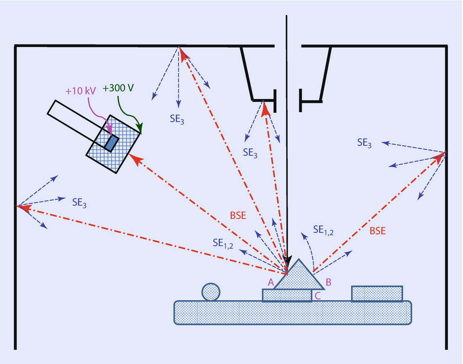
Schematic illustration of the various sources of signals generated from topography: BSEs, SE1 and SE2, and remote SE3 and collection by the Everhart–Thornley detector

7.3.2 The Light-Optical Analogy to the SEM/E–T (Positive Bias) Image

The complex mix of direct BSEs, SE1 and SE2, and remote SE3 illustrated in ◘ Fig. 7.4 effectively illuminates the specimen in a way similar to the “real world” landscape scene illustrated schematically in ◘ Fig. 7.5 (Oatley 1972). A viewer in an airplane looks down on a hilly landscape that is directionally illuminated by the Sun at a shallow (oblique) angle, highlighting sloping hillsides such as “A,” while a general pattern of diffuse light originates from scattering of sunlight by clouds and the atmosphere that illuminates all features, including those not in the direct path of the sunlight, such as hillside “B,” while the cave “C” receives no illumination. To establish this light-optical analogy, we must match components with similar characteristics:
../images/271173_4_En_7_Chapter/271173_4_En_7_Fig5_HTML.png
Fig. 7.5

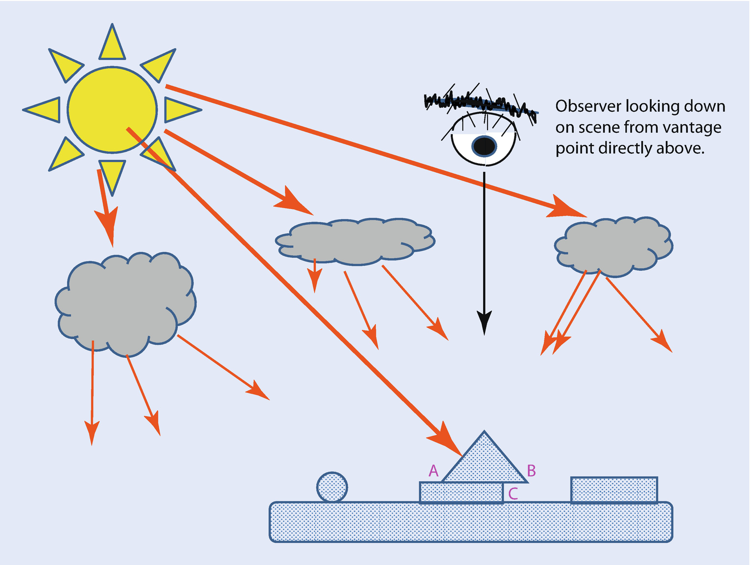
Human visual experience equivalent to the observer position and lighting situation of the Everhart–Thornley (positive bias) detector

  1. 1.

    The human observer’s eye, which has a very sharply defined line-of-sight, is matched in characteristic by the electron beam, which presents a very narrow cone angle of rays: thus, the observer of an SEM image is effectively looking along the beam, and what the beam can strike is what can be observed in an image.

     
  2. 2.

    The illumination of an outdoor scene by the Sun consists of a direct component (direct rays that strongly light those surfaces that they strike) and an indirect component (diffuse scattering of the Sun’s rays from clouds and the atmosphere, weakly illuminating the scene from all angles). For the E–T detector (positive bias), there is a direct signal component that acts like the Sun (BSEs emitted by the specimen into the solid angle defined by the scintillator, as well as SE1 and SE2 directly collected from the specimen) and an indirect component that acts like diffuse illumination (SE3 collected from all surfaces struck by BSEs).


Though counterintuitive, in the SEM the detector is the apparent source of illumination while the observer looks along the electron beam.

7.3.2.1 Establishing a Robust Light-Optical Analogy

The human visual process has developed in a world of top lighting (◘ Fig. 7.6): sunlight comes from above in the outdoors; our indoor environment is illuminated from light sources on the ceiling or lamp fixtures placed above our comfortable reading chair. We instinctively expect that brightly illuminated features must be facing upward to receive light from the source above, while poorly illuminated features are facing away from the light source. Thus, to establish the strongest possible light-optical analogy for the SEM/E–T (positive bias) image, we need to create a situation of apparent top lighting. Because the strong source of apparent illumination in an SEM image appears to come from the detector (direct BSEs, SE1, and SE2 for an E–T [positive bias] detector), by ensuring that the effective location of the E–T detector is at the top of the SEM image field as it is presented to the viewer, any feature facing the E–T detector will appear bright, thus establishing that the apparent lighting of the scene presented to the viewer will be from above. All features that can be reached by the electron beam will produce some signal, even those facing away from the E–T (positive bias) detector or that are screened by local topography, through the collection of the SE3 component. Thus, if we imagine the specimen scene to be illuminated by a primary light source, then that light source occupies the position of the E–T detector and the viewer of that scene is looking along the electron beam. The SE3 component of the signal provides a general diffuse secondary source of illumination that appears to come from all directions.
../images/271173_4_En_7_Chapter/271173_4_En_7_Fig6_HTML.png
Fig. 7.6

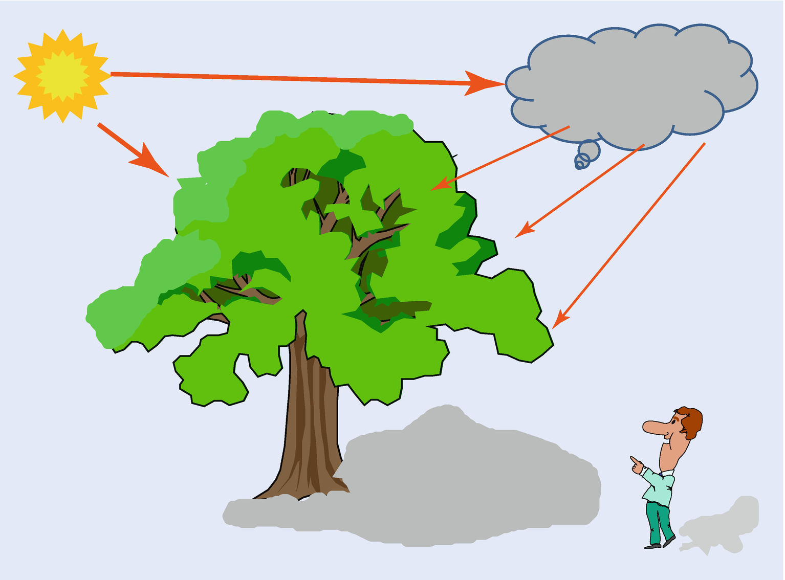
We have evolved in a world of top lighting. Features facing the Sun are brightly illuminated, while features facing away are shaded but receive some illumination from atmospheric scattering. Bright = facing upwards

7.3.2.2 Getting It Wrong: Breaking the Light-Optical Analogy of the Everhart–Thornley (Positive Bias) Detector

If the microscopist is not careful, it is possible to break the light-optical analogy of the Everhart-Thornley (positive bias) detector. This situation can arise through improper collection of the image by misuse of the feature called “Scan Rotation” (or in subsequent off-line image modification with image processing software). “Scan Rotation” is a commonly available feature of nearly all SEM systems that allows the microscopist to arbitrarily orient an image on the display screen. While this may seem to be a useful feature that enables the presentation of the features of a specimen in a more aesthetically pleasing manner (e.g., aligning a fiber along the long axis of a rectangular image), scan rotation changes the apparent position of the E–T detector (indeed, of all detectors) in the image with potentially serious consequences that can compromise the light-optical analogy of the E–T (positive bias) detector. The observer is naturally accustomed to having top illumination when interpreting images of topography, that is, the apparent source of illumination coming from the top of the field-of-view and shining down on the features of the specimen. When the top lighting condition is violated and the observer is unaware of the alteration of the scene illumination, then the sense of the topography can appear inverted. Arbitrary scan rotation can effectively place the E–T detector, or any other asymmetrically placed (i.e., off-axis) detector, at the bottom or sides of the image, and if the observer is unaware of this situation of unfamiliar illumination, misinterpretation of the specimen topography is likely to result. This is especially true in the case of specimens for which there are limited visual clues. For example, the SEM image of an insect contains many familiar features—e.g., head, eyes, legs, etc.—that make it almost impossible to invert the topography regardless of the apparent lighting. By comparison, the image of an undulating surface of an unknown object may provide no clues that cause the proper sense of the topography to “click in” for the observer. Having top illumination is critical in such cases. When a microscopist works in a multi-user facility, the possibility must always be considered that a previous user may have arbitrarily adjusted the scan rotation. As part of a personal quality-assurance plan, the careful microscopist should confirm that the location of the E–T detector is at the top center of the image. ◘ Figure 7.7 demonstrates a procedure that enables unambiguous location of the E–T detector. Some (but not all) implementations of the E–T detector enable the user to “deconstruct” the E–T detector image by selectively excluding the SE component of the total signal—either by changing the Faraday cage voltage to negative values to reject the very low energy SEs (e.g., −50 V cage bias) or by eliminating the high potential on the scintillator so that SEs cannot be accelerated to sufficient kinetic energy to excite scintillation. Even without the high potential applied to the scintillator, the E–T detector remains sensitive to the high energy BSEs generated by a high energy primary beam, for example., E 0 ≥ 20 keV, which creates a large fraction of BSEs with energy >10 keV. As a passive scintillator or with the negative Faraday cage potential applied, the E–T (negative bias) detector only collects the small fraction of high energy BSEs scattered into the solid angle defined by the E–T scintillator. When the direct BSE mode of the E–T (negative bias) detector is selected, debris on a flat surface is found to create distinct shadows that point away from the apparent source of illumination, the E–T detector. By using the scan rotation, the effective position of the E–T detector can then be moved to the top of the image, as shown in the sequence of ◘ Fig. 7.7a–c, thus achieving the desired top-lighting situation. When the conventional E–T (positive bias) is used to image this same field of view (◘ Fig. 7.7d), the strong shadow of the particle disappears because of the efficient collection of SEs, particularly the SE3 component, and now has a bright edge along the top which reinforces the impression that it rises above the general surface.
../images/271173_4_En_7_Chapter/271173_4_En_7_Fig7_HTML.jpg
Fig. 7.7

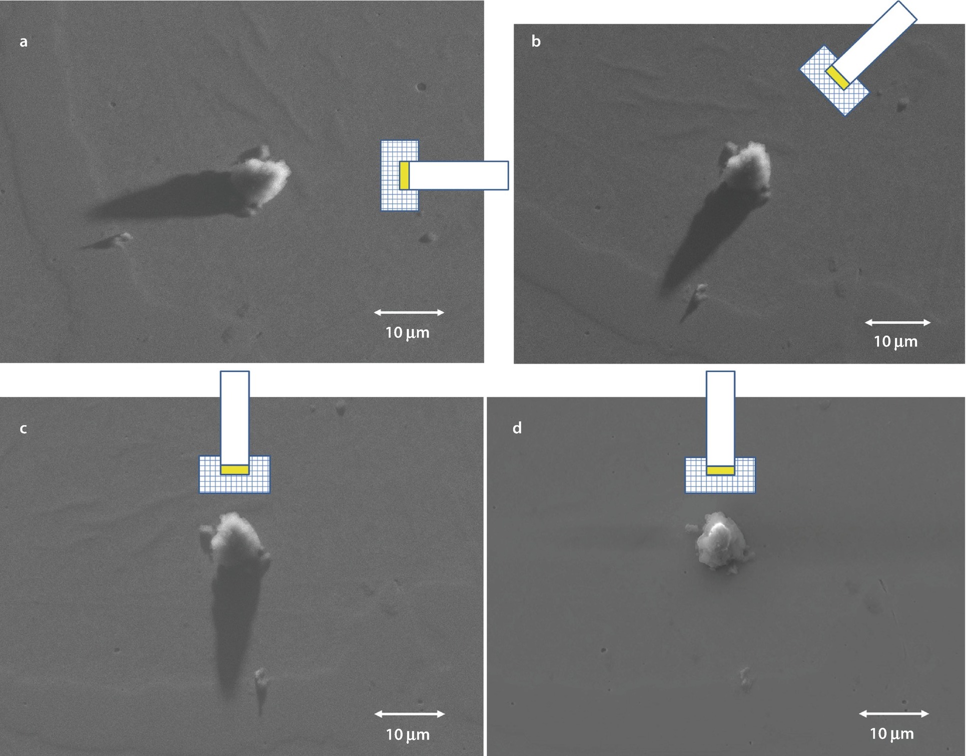
a SEM image of a particle on a surface as prepared with the E–T (negative bias) detector in the 90° clockwise position shown; E 0 = 20 keV. Note strong shadowing pointing away from E–T . b SEM image of a particle on a surface as prepared with the E–T (negative bias) detector in the 45° clockwise position shown; E 0 = 20 keV. Note strong shadowing pointing away from E–T . c SEM image of a particle on a surface as prepared with the E–T (negative bias) detector in the 0° clockwise (12 o’clock) position shown; E 0 = 20 keV. Note strong shadowing pointing away from E–T . d SEM image of a particle on a surface as prepared with the E–T (positive bias) detector in the 0° clockwise (12 o’clock) position shown; E 0 = 20 keV. Note lack of shadowing but bright surface facing the E–T (positive bias) detector

Note that physically rotating the specimen stage to change the angular relation of the specimen relative to the E–T (or any other) detector does not change the location of the apparent source of illumination in the displayed image. Rotating the specimen stage changes which specimen features are directed toward the detector, but the scan orientation on the displayed image determines the relative position of the detector in the image presented to the viewer and the apparent direction of the illumination.

7.3.2.3 Deconstructing the SEM/E–T Image of Topography

It is often useful to examine the separate SE and BSE components of the E–T detector image. An example of a blocky fragment of pyrite (FeS2) imaged with a positively-biased E–T detector is shown in ◘ Fig. 7.8a. In this image, the effective position of the E–T detector relative to the presentation of the image is at the top center. ◘ Figure 7.8b shows the same field of view with the Faraday cage biased negatively to exclude SEs so that only direct BSEs contribute to the SEM image. The image contrast is now extremely harsh, since topographic features facing toward the detector are illuminated, while those facing away are completely lost. Comparing ◘ Fig. 7.8a, b, the features that appear bright in the BSE-only image are also brighter in the full BSE + SE image obtained with the positively biased E–T detector, demonstrating the presence of the direct-BSE component. The much softer contrast of nearly all surfaces seen in the BSE + SE image of ◘ Fig. 7.8a demonstrates the efficiency of the E–T detector for collection of signal from virtually all surfaces of the specimen that the primary beam strikes.
../images/271173_4_En_7_Chapter/271173_4_En_7_Fig8_HTML.jpg
Fig. 7.8

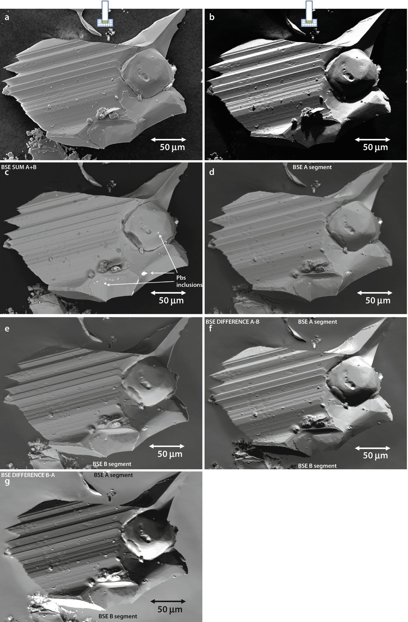
a SEM/E–T (positive bias) image of a fractured fragment of pyrite; E 0 = 20 keV. b SEM/E–T (negative bias) image of a fractured fragment of pyrite; E 0 = 20 keV. c SEM/BSE (A + B) SUM-mode image of a fractured fragment of pyrite; E 0 = 20 keV. d SEM/BSE (A segment) image (detector at top of image field) of a fractured fragment of pyrite (FeS2); E 0 = 20 keV. e SEM/BSE (B segment) image (detector at bottom of image field) of a fractured fragment of pyrite (FeS2); E 0 = 20 keV. f SEM/BSE (A−B) image (detector DIFFERENCE image) of a fractured fragment of pyrite (FeS2); E 0 = 20 keV. g SEM/BSE (B−A) image (detector DIFFERENCE image) of a fractured fragment of pyrite (FeS2); E 0 = 20 keV

7.3.3 Imaging Specimen Topography With a Semiconductor BSE Detector

A segmented (A and B semicircular segments) semiconductor BSE detector placed directly above the specimen is illustrated schematically in ◘ Fig. 7.9. This BSE detector is mounted below the final lens and is placed symmetrically around the beam, so that in the summation mode it acts as an annular detector. A simple topographic specimen is illustrated, oriented so that the left face directs BSEs toward the A-segment, while the right face directs BSEs toward the B-segment. This A and B detector pair is typically arranged so that one of the segments, “A,” is oriented so that it appears to illuminate from the top of the image, while the “B” segment appears to illuminate from the bottom of the image. The segmented detector enables selection of several modes of operation: SUM mode (A + B), DIFFERENCE mode (A−B), and individual detectors A or B) (Kimoto and Hashimoto 1966).
../images/271173_4_En_7_Chapter/271173_4_En_7_Fig9_HTML.jpg
Fig. 7.9

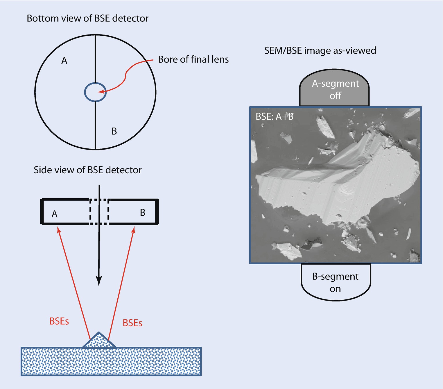
Schematic illustration of a segmented annular semiconductor BSE detector

7.3.3.1 SUM Mode (A + B)

The two-segment semiconductor BSE detector operating in the summation (A + B) mode was used to image the same pyrite specimen previously imaged with the E–T (positive bias) and E–T (negative bias), as shown in ◘ Fig. 7.8c. The placement of the large solid angle BSE is so close to the primary electron beam that it creates the effect of apparent wide-angle illumination that is highly directional along the line-of-sight of the observer, which would be the light-optical equivalent of being inside a flashlight looking along the beam. With such directional illumination along the observer’s line-of-sight, the brightest topographic features are those oriented perpendicular to the line-of-sight, while tilted surfaces appear darker, resulting in a substantially different impression of the topography of the pyrite specimen compared to the E–T (positive bias) image in ◘ Fig. 7.8a. The large solid angle of the detector acts to suppress topographic contrast, since local differences in the directionality of BSE emission caused by differently inclined surfaces are effectively eliminated when the diverging BSEs are intercepted by another part of the large BSE detector.

Another effect that is observed in the A + B image is the class of very bright inclusions which were subsequently determined to be galena (PbS) by X-ray microanalysis. The large difference in average atomic number between FeS2 (Z av = 20.7) and PbS (Z av = 73.2) results in strong atomic number (compositional) between the PbS inclusions and the FeS2 matrix. Although there is a significant BSE signal component in the E–T (positive bias) image in ◘ Fig. 7.8a, the topographic contrast is so strong that it overwhelms the compositional contrast.

7.3.3.2 Examining Images Prepared With the Individual Detector Segments

Some semiconductor BSE detector systems enable the microscopist to view BSE images prepared with the signal derived from the individual components of a segmented detector. As illustrated in ◘ Fig. 7.9 for a two-segment BSE detector, the individual segments effectively provide an off-axis, asymmetric illumination of the specimen. Comparing the A-segment and B-segment images of the pyrite crystal in ◘ Fig. 7.8d, e, the features facing each detector can be discerned and a sense of the topography can be obtained by comparing the two images. But note the strong effect of the apparent inversion of the sense of the topography in the B-segment image, where the illumination comes from the bottom of the field, compared to the A-segment image, where the illumination comes from the top of the field of view.

7.3.3.3 DIFFERENCE Mode (A−B)

The signals from the individual BSE detector segments “A” and “B” can be subtracted from each other, producing the image seen in ◘ Fig. 7.8f. Because the detector segments “A” and “B” effectively illuminate the specimen from two different directions, as seen in ◘ Fig. 7.8d, e, taking the difference A–B between the detector signals tends to enhance these directional differences, producing the strong contrast seen in ◘ Fig. 7.8f.

Note that when subtracting the signals the order of the segments in the subtraction has a profound effect on appearance of the final image. ◘ Figure 7.8g shows the image created with the order of subtraction reversed to give B–A. Because the observer is so strongly biased toward interpreting an image as if it must have top lighting, bright features are automatically interpreted as facing upward. This automatic assumption of top lighting has the effect for most viewers of ◘ Fig. 7.8g to strongly invert the apparent sense of the topography, so that protuberances in the A–B image become concavities in the B–A image. If BSE detector difference images are to be at all useful and not misleading, it is critical to determine the proper order of subtraction. A suitable test procedure is to image a specimen with known topography, such as the raised lettering on a coin or a particle standing on top of a flat surface.

Creative Commons

Open Access This chapter is licensed under the terms of the Creative Commons Attribution-NonCommercial 2.5 International License (http://creativecommons.org/licenses/by-nc/2.5/), which permits any noncommercial use, sharing, adaptation, distribution and reproduction in any medium or format, as long as you give appropriate credit to the original author(s) and the source, provide a link to the Creative Commons license and indicate if changes were made.

The images or other third party material in this chapter are included in the chapter's Creative Commons license, unless indicated otherwise in a credit line to the material. If material is not included in the chapter's Creative Commons license and your intended use is not permitted by statutory regulation or exceeds the permitted use, you will need to obtain permission directly from the copyright holder.