© Springer Science+Business Media LLC 2018
Joseph I. Goldstein, Dale E. Newbury, Joseph R. Michael, Nicholas W.M. Ritchie, John Henry J. Scott and David C. JoyScanning Electron Microscopy and X-Ray Microanalysishttps://doi.org/10.1007/978-1-4939-6676-9_9

9. Image Defects

Joseph I. Goldstein1 , Dale E. Newbury2, Joseph R. Michael3, Nicholas W. M. Ritchie2, John Henry J. Scott2 and David C. Joy4
(1)
University of Massachusetts, Amherst, Massachusetts, USA
(2)
National Institute of Standards and Technology, Gaithersburg, Maryland, USA
(3)
Sandia National Laboratories, Albuquerque, New Mexico, USA
(4)
University of Tennessee, Knoxville, Tennessee, USA
 

SEM images are subject to defects that can arise from a variety of mechanisms, including charging, radiation damage, contamination, and moiré fringe effects, among others. Image defects are very dependent on the specific nature of the specimen, and often they are anecdotal, experienced but not reported in the SEM literature. The examples described below are not a complete catalog but are presented to alert the microscopist to the possibility of such image defects so as to avoid interpreting artifact as fact.

9.1 Charging

Charging is one of the major image defects commonly encountered in SEM imaging, especially when using the Everhart–Thornley (positive bias) “secondary electron” detector, which is especially sensitive to even slight charging.

9.1.1 What Is Specimen Charging?

The specimen can be thought of as an electrical junction into which the beam current, i B, flows. The phenomena of backscattering of the beam electrons and secondary electron emission represent currents flowing out of the junction, i BSE (= η i B) and i SE (= δ i B). For a copper target and an incident beam energy of 20 keV, η is approximately 0.3 and δ is approximately 0.1, which together account for 0.4 or 40 % of the charges injected into the specimen by the beam current. The remaining beam current must flow from the specimen to ground to avoid the accumulation of charge in the junction (Kirchoff’s current law). The balance of the currents for a non-charging junction is then given by

$$ \sum {i}_{\mathrm{in}}=\sum {i}_{\mathrm{out}} $$

$$ {i}_{\mathrm{B}}={i}_{\mathrm{B}\mathrm{SE}}+{i}_{\mathrm{SE}}+{i}_{\mathrm{SC}} $$
(9.1)
where i SC is the specimen (or absorbed) current. For the example of copper, i SC = 0.6 i B.
The specimen stage is typically constructed so that the specimen is electrically isolated from electrical ground to permit various measurements. A wire connection to the stage establishes the conduction path for the specimen current to travel to the electrical ground. This design enables a current meter to be installed in this path to ground, allowing direct measurement of the specimen current and enabling measurement of the true beam current with a Faraday cup (which captures all electrons that enter it) in place of the specimen. Moreover, this specimen current signal can be used to form an image of the specimen (see the “Electron Detectors” module) However, if the electrical path from the specimen surface to ground is interrupted, the conditions for charge balance in Eq. (9.1) cannot be established, even if the specimen is a metallic conductor. The electrons injected into the specimen by the beam will then accumulate, and the specimen will develop a high negative electrical charge relative to ground. The electrical field from this negative charge will decelerate the incoming beam electrons, and in extreme cases the specimen will actually act like an electron mirror. The scanning beam will be reflected before reaching the surface, so that it actually scans the inside of the specimen chamber, creating an image that reveals the objective lens, detectors, and other features of the specimen chamber, as shown in ◘ Fig. 9.1.
../images/271173_4_En_9_Chapter/271173_4_En_9_Fig1_HTML.jpg
Fig. 9.1

SEM image (Everhart–Thornley detector, positive bias) obtained by disconnecting grounding wire from the specimen stage and reflecting the scan from a flat, conducting substrate; E 0 = 1 keV

If the electrical path to ground is established, then the excess charges will be dissipated in the form of the specimen current provided the specimen has sufficient conductivity. Because all materials (except superconductors) have the property of electrical resistivity, ρ, the specimen has a resistance R (R = ρ L/A, where L is the length of the specimen and A is the cross section), and the passage of the specimen current, i SC, through this resistance will cause a potential drop across the specimen, V = i SC R. For a metal, ρ is typically of the order of 10−6 Ω-cm, so that a specimen 1-cm thick with a cross-sectional area of 1 cm2 will have a resistance of 10−6 Ω, and a beam current of 1 nA (10−9 A) will cause a potential of about 10−15 V to develop across the specimen. For a high purity (undoped) semiconductor such as silicon or germanium, ρ is approximately 104 to 106 Ω-cm, and the 1-nA beam will cause a potential of 1 mV (10−3 V) or less to develop across the 1-cm cube specimen, which is still negligible. The flow of the specimen current to ground becomes a critical problem when dealing with non-conducting (insulating) specimens. Insulating specimens include a very wide variety of materials such as plastics, polymers, elastomers, minerals, rocks, glasses, ceramics, and others, which may be encountered as bulk solids, porous solids, foams, particles, or fibers. Virtually all biological specimens become non-conducting when water is removed by drying, substitution with low vapor pressure polymers, or frozen in place. For an insulator such as an oxide, ρ is very high, 106 to 1016 Ω-cm, which prevents the smooth motion of the electrons injected by the beam through the specimen to ground; electrons accumulate in the immediate vicinity of the beam impact, raising the local potential and creating a range of phenomena described as “charging.”

9.1.2 Recognizing Charging Phenomena in SEM Images

Charging phenomena cover a wide range of observed behaviors in SEM images of imperfectly conducting specimens. Secondary electrons (SEs) are emitted with very low energy, by definition E SE < 50 eV, with most carrying less than 5 eV. Such low energy, slow-moving SEs can be strongly deflected by local electrical fields caused by charging. The Everhart–Thornley (positive bias) detector collects SEs by means of a positive potential of a few hundred volts (e.g., +300 V) applied to the Faraday cage at a distance of several centimeters (e.g., 3 cm) from the specimen, creating an electrical field at the specimen of approximately 104 V/m. SEs emitted from a conducting specimen are strongly attracted to follow the field lines from the grounded specimen surface to the positively biased Faraday cage grid, and thus into the high voltage field applied to the face of the scintillator of the Everhart–Thornley (E–T) detector. If the specimen charges locally to develop even a few volts’ potential, the local electrical field from the charged region relative to nearby uncharged areas of the specimen a few micrometers away or to the grounded stub a few millimeters away is likely to be much stronger (105 to 107 V/m) than the field imposed by the E–T detector. Depending on the positive or negative character, this specimen field may have either a repulsive or an attractive effect. Thus, depending on the details of the local electrical field, the collection of SEs by the E–T detector may be enhanced or diminished. Negatively charging areas will appear bright, while in positively charging areas the SEs are attracted back to the specimen surface or to the stub so that such a region appears dark. Thus, the typical appearance of an isolated insulating particle undergoing charging on a conducting surface is a bright, often saturated signal (possibly accompanied by amplifier overloading effects due to signal saturation) surrounded by a dark halo that extends over surrounding conducting portions of the specimen where the local field induced by the charging causes the SEs to be recollected. This type of voltage contrast must be regarded as an artifact, because it interferes with and overwhelms the regular behavior of secondary electron (SE) emission with local surface inclination that we depend upon for sensible image interpretation of specimen topography with the E–T detector. ◘ Figure 9.2 shows examples of charging effects observed when imaging insulating particles on a conducting metallic substrate with the E–T (positive bias) detector. There are regions on the particles that are extremely bright due to high negative charging that increases the detector collection efficiency surrounded by a dark “halo” where a positive mirror charge develops, lowering the collection efficiency. Often these charging effects, while extreme in the E–T (positive bias) image due to the disruption of SE trajectories, will be negligible in a backscattered electron (BSE) image simultaneously collected from the same field of view, because the much higher energy BSEs are not significantly deflected by the low surface potential. An example is shown in ◘ Fig. 9.3, where the SE image, ◘ Fig. 9.3a, shows extreme bright-dark regions due to charging while the corresponding BSE image, ◘ Fig. 9.3b, shows details of the structure of the particle. In more extreme cases of charging, the true topographic contrast image of the specimen may be completely overwhelmed by the charging effects, which in the most extreme cases will actually deflect the beam causing image discontinuities. An example is shown in ◘ Fig. 9.4, which compares images (Everhart–Thornley detector, positive bias) of an uncoated calcite crystal at E 0 = 1.5 keV, where the true shape of the object can be seen, and at E 0 = 5 keV, where charging completely overwhelms the topographic contrast.
../images/271173_4_En_9_Chapter/271173_4_En_9_Fig2_HTML.jpg
Fig. 9.2

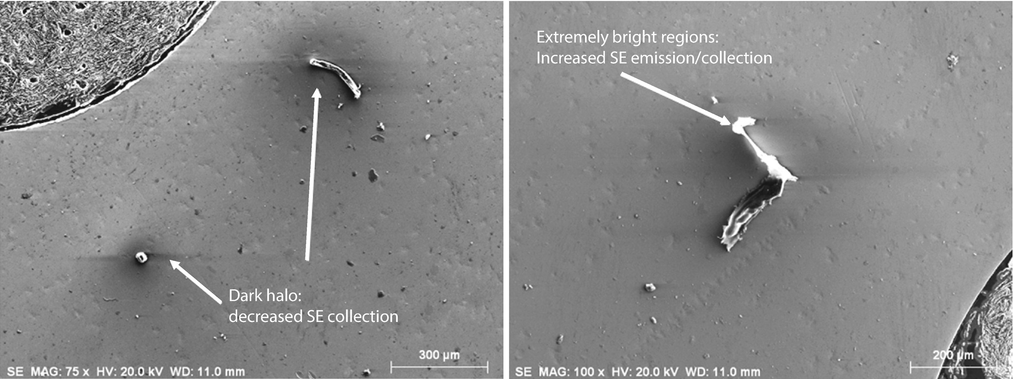
Examples of charging artifacts observed in images of dust particles on a metallic substrate. E 0 = 20 keV; Everhart–Thornley (positive bias) detector

../images/271173_4_En_9_Chapter/271173_4_En_9_Fig3_HTML.jpg
Fig. 9.3

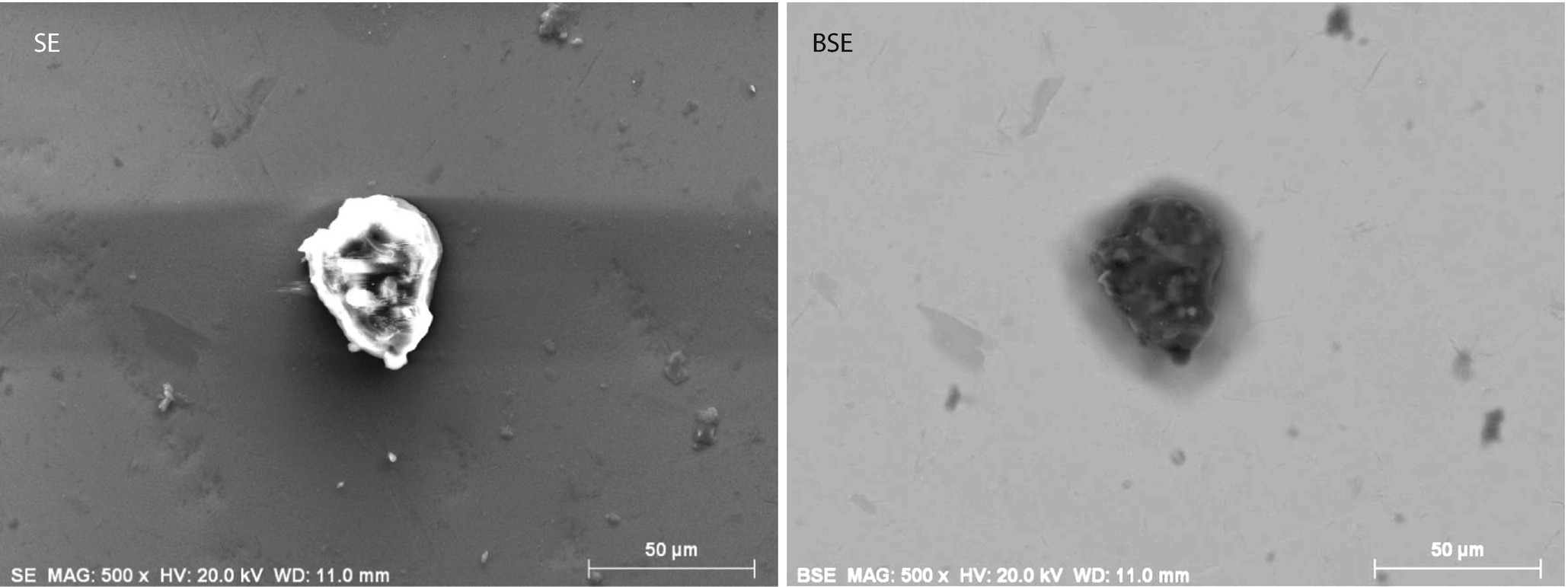
Comparison of images of a dust particle on a metallic substrate: (left) Everhart–Thornley (positive bias) detector; (right) semiconductor BSE (sum) detector; E 0 = 20 keV

../images/271173_4_En_9_Chapter/271173_4_En_9_Fig4_HTML.jpg
Fig. 9.4

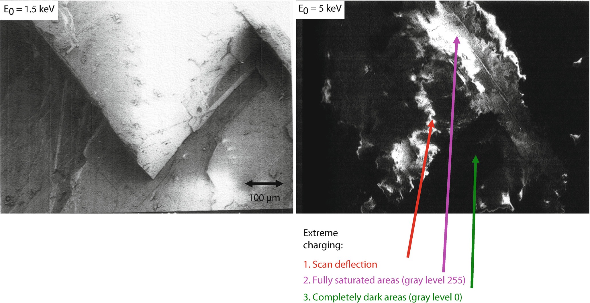
Comparison of images of an uncoated calcite crystal viewed at (left) E 0 = 1.5 keV, showing topographic contrast; (right) E 0 = 5 keV, showing extreme charging effects; Everhart–Thornley (positive bias) detector

Charging phenomena are incompletely understood and are often found to be dynamic with time, a result of the time-dependent motion of the beam due to scanning action and due to the electrical breakdown properties of materials as well as differences in surface and bulk resistivity. An insulating specimen acts as a local capacitor, so that placing the beam at a pixel causes a charge to build up with an RC time constant as a function of the dwell time, followed by a decay of that charge when the beam moves away. Depending on the exact material properties, especially the surface resistivity which is often much lower than the bulk resistivity, and the beam conditions (beam energy, current, and scan rate), the injected charge may only partially dissipate before the beam returns in the scan cycle, leading to strong effects in SEM images. Moreover, local specimen properties may cause charging effects to vary with position in the same image. A time-dependent charging situation at a pixel is shown schematically in ◘ Fig. 9.5, where the surface potential at a particular pixel accumulates with the dwell time and then decays until the beam returns. In more extreme behavior, the accumulated charge may cause local electrical breakdown and abruptly discharge to ground. The time dependence of charging can result in very different imaging results as the pixel dwell time is changed from rapid scanning for surveying a specimen to slow scanning for recording images with better signal-to-noise. An example of this phenomenon is shown in ◘ Fig. 9.6, where an image of an uncoated mineral fragment taken with E 0 = 1 keV appears to be free of charging artifacts with a pixel dwell time of 1.6 μs, but longer dwell times lead to the in-growth of a bright region due to charging. Charging artifacts can often be minimized by avoiding slow scanning through the use of rapid scanning and summing repeated scans to improve the signal-to-noise of the final image.
../images/271173_4_En_9_Chapter/271173_4_En_9_Fig5_HTML.png
Fig. 9.5

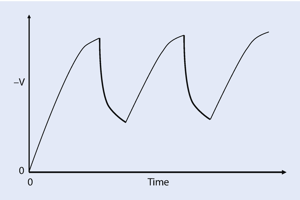
Schematic illustration of the potential developed at a pixel as a function of time showing repeated beam dwells

../images/271173_4_En_9_Chapter/271173_4_En_9_Fig6_HTML.jpg
Fig. 9.6

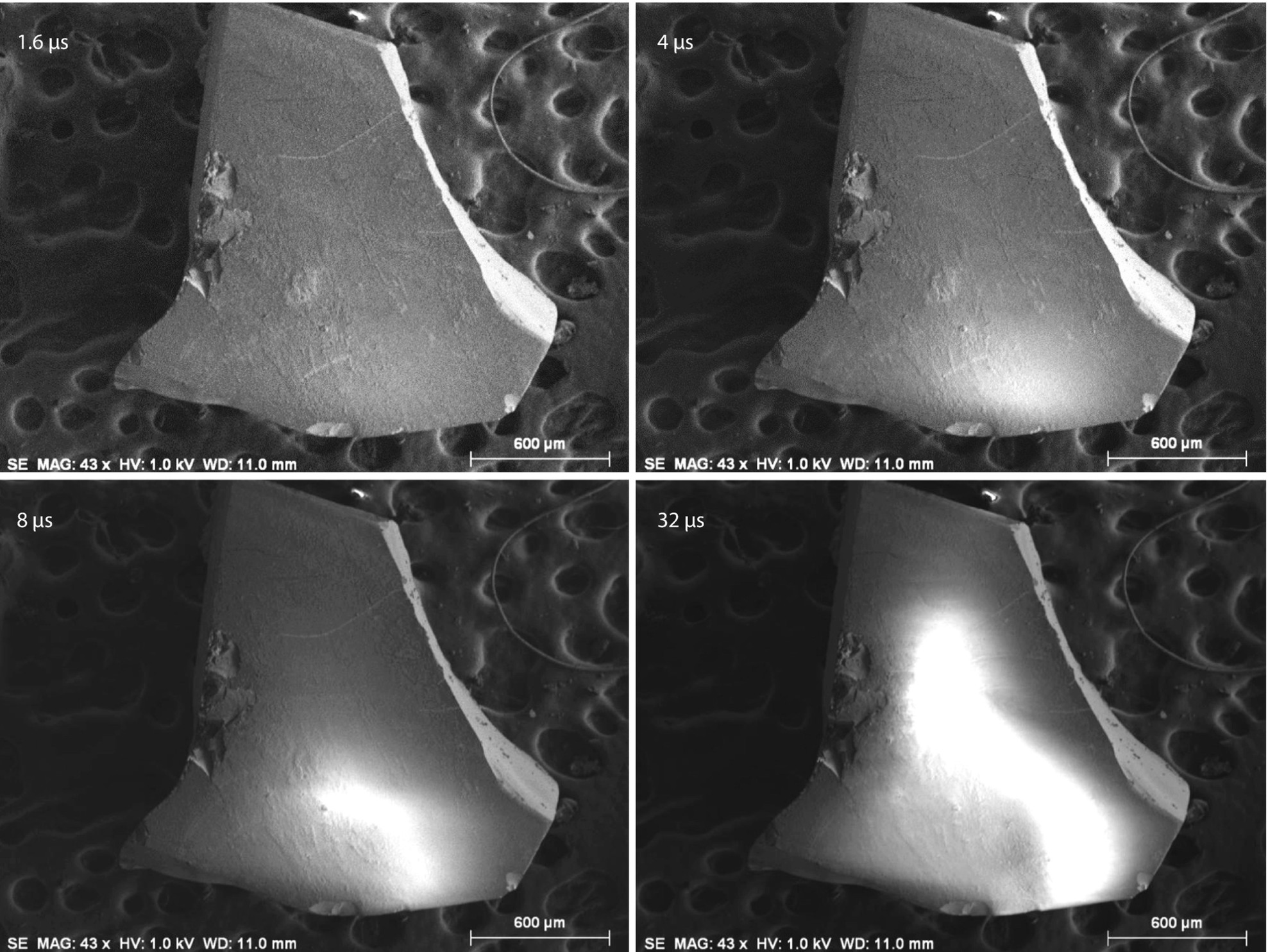
Sequence of images of an uncoated quartz fragment imaged at E 0 = 1 keV with increasing pixel dwell times, showing development of charging; Everhart–Thornley (positive bias) detector

Charging of some specimens can create contrast that can easily be misinterpreted as specimen features. An example is shown in ◘ Fig. 9.7, where most of the polystyrene latex spheres (PSLs) imaged at E 0 = 1 keV with the Everhart–Thornley (positive bias) detector show true topographic details, but five of the PSLs have bright dots at the center, which might easily be mistaken for high atomic number inclusions or fine scale topographic features rising above the spherical surfaces. Raising the beam energy to 1.5 keV and higher reveals progressively more extensive and obvious evidence of charging artifacts. The nature of this charging artifact is revealed in ◘ Fig. 9.8, which compares an image of the PSLs at higher magnification and E 0 = 5 keV with a low magnification image of a large plastic sphere (5 mm in diameter) that was first subjected to bombardment at E 0 = 10 keV, followed by imaging at E 0 = 2 keV where the deposited charge acts to reflect the beam and produce a “fish-eye” lens view of the SEM chamber. Close examination of the higher magnification PSL images shows that each of these microscopic spheres is acting like a tiny “fish-eye lens” and producing a highly distorted view of the SEM chamber.
../images/271173_4_En_9_Chapter/271173_4_En_9_Fig7_HTML.jpg
Fig. 9.7

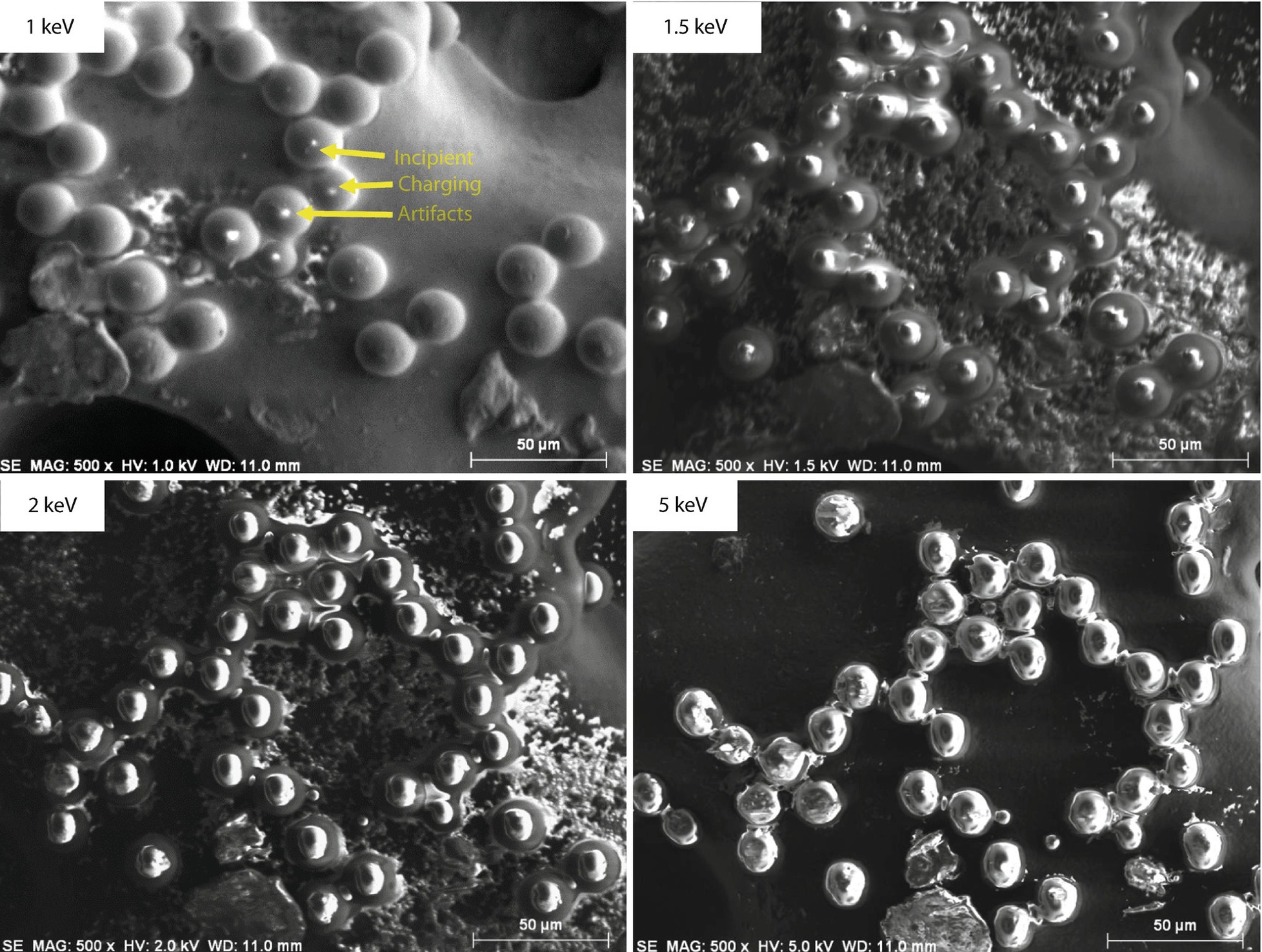
Polystyrene latex spheres imaged over a range of beam energy, showing development of charging artifacts; Everhart–Thornley (positive bias) detector

../images/271173_4_En_9_Chapter/271173_4_En_9_Fig8_HTML.jpg
Fig. 9.8

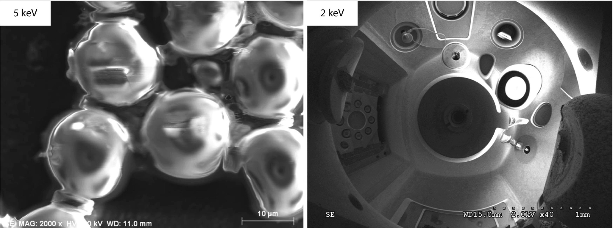
(left) Higher magnification image of PSLs at E 0 = 5 keV; (right) reflection image from large plastic sphere that was charged at E 0 = 10 keV and then imaged at E 0 = 2 keV; Everhart–Thornley (positive bias) detector

9.1.3 Techniques to Control Charging Artifacts (High Vacuum Instruments)

9.1.3.1 Observing Uncoated Specimens

To understand the basic charging behavior of an uncoated insulator imaged with different selections of the incident beam energy, consider ◘ Fig. 9.9, which shows the behavior of the processes of backscattering and secondary electron emission as a function of beam energy. For beam energies above 5 keV, generally η + δ < 1, so that more electrons are injected into the specimen by the beam than leave as BSEs and SEs, leading to an accumulation of negative charge in an insulator. For most materials, especially insulators, as the beam energy is lowered, the total emission of BSEs and SEs increases, eventually reaching an upper cross-over energy, E 2 (which typically lies in the range 2–5 keV depending on the material) where η + δ = 1, and the charge injected by the beam is just balanced by the charge leaving as BSEs and SEs. If a beam energy is selected just above E 2 where η + δ < 1, the local build-up of negative charge acts to repel the subsequent incoming beam electrons while the beam remains at that pixel, lowering the effective kinetic energy with which the beam strikes the surface eventually reaching the E 2 energy and a dynamically stable charge balance. For beam energies below the E 2 value and above the lower cross-over energy E 1 (approximately 0.5–2 keV, depending on the material), the emission of SE can actually reach very large values for insulators with δ max ranging from 2 to 20 depending on the material. Thus, in this beam energy region η + δ > 1, resulting in positive charging which increases the kinetic energy of the incoming beam electrons until the E 2 energy is reached and charge balance occurs. This dynamic charge stability enables uncoated insulators to be imaged, as shown in the example of the uncoated mineral particle shown in ◘ Fig. 9.10, where a charge-free image is obtained at E 0 = 1 keV, but charging effects are observed at E 0 ≥ 2 keV. Achieving effective “dynamic charge balance microscopy” is sensitive to material and specimen shape (local tilt as it affects BSEs and particularly SE emission), and success depends on optimizing several instrument parameters: beam energy, beam current, and scan speed. Note that the uncoated mineral specimen used in the beam energy sequence in ◘ Fig. 9.10 is the same used for the pixel dwell time sequence at E 0 = 1 keV in ◘ Fig. 9.6 where charging is observed when longer dwell times are used, demonstrating the complex response of charging to multiple variables.
../images/271173_4_En_9_Chapter/271173_4_En_9_Fig9_HTML.png
Fig. 9.9

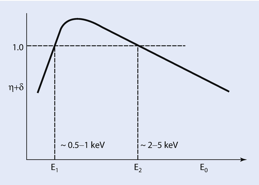
Schematic illustration of the total emission of backscattered electrons and secondary electrons as a function of incident beam energy; note upper and lower cross-over energies where η + δ = 1

../images/271173_4_En_9_Chapter/271173_4_En_9_Fig10_HTML.jpg
Fig. 9.10

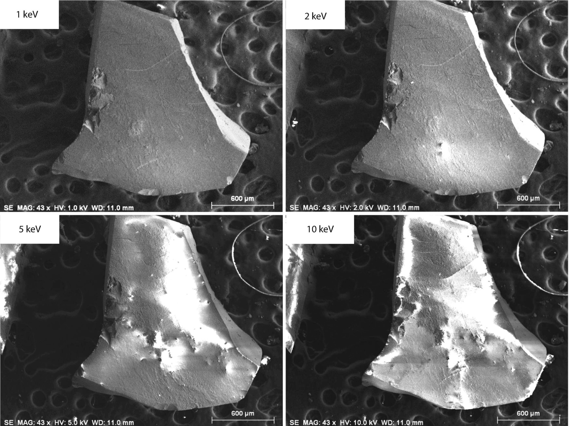
Beam energy sequence showing development of charging as the energy is increased. Specimen: uncoated quartz fragment; 1.6 μs per pixel dwell time; Everhart–Thornley (positive bias) detector

9.1.3.2 Coating an Insulating Specimen for Charge Dissipation

Conductive coatings can be deposited by thermal evaporation with electron beam heating (metals, alloys) or with resistive heating (carbon), by high energy ion beam sputtering (metals, alloys), or by low energy plasma ion sputtering (alloys). The coating must cover all of the specimen, including complex topographic shapes, to provide a continuous conducting path across the surface to dissipate the charge injected into the specimen by the electron beam. It is important to coat all surfaces that are directly exposed to the electron beam or which might receive charge from BSEs, possibly after re-scattering of those BSEs. Note that applying a conductive coating alone may not be sufficient to achieve efficient charge dissipation. Many specimens may be so thick that the sides may not actually receive an adequate amount of the coating material, as illustrated in ◘ Fig. 9.11, even with rotation during the coating process. It is necessary to complete the path from the coating to the electrical ground with a conducting material that exhibits a low vapor pressure material that is compatible with the microscope’s vacuum requirement, such as a metal wire, conducting tape, or metal foil.
../images/271173_4_En_9_Chapter/271173_4_En_9_Fig11_HTML.png
Fig. 9.11

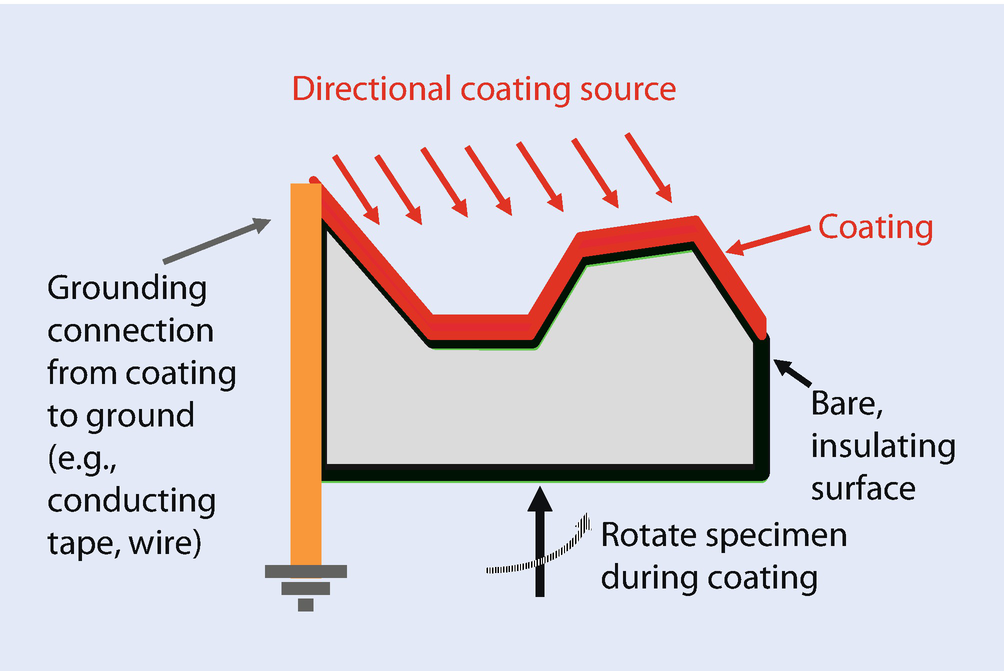
Schematic diagram showing the need to provide a grounding path from a surface coating due to uncoated or poorly coated sides of a non-conducting specimen

It is desirable to make the coating as thin as possible, and for many samples an effective conducting film can be 2–10 nm in thickness. A beam with E 0 > 5 keV will penetrate through this coating and 10–100 times (or more) deeper depending on material and the incident beam energy, thus depositing most of the charge in the insulator itself. However, the presence of a ground plane and conducting path nanometers to micrometers away from the implanted charge creates a very high local field gradient, >106 V/m, apparently leading to continuous breakdown and discharging. The strongest evidence that a continuous discharge situation is established that avoids the build-up of charge is the behavior of the Duane–Hunt energy limit of the X-ray continuum. As the beam electrons are decelerated in the Coulombic field of the atoms, the energy lost is emitted as photons of electromagnetic radiation, termed bremsstrahlung, or braking radiation, and forming a continuous spectrum of photon energies up to the incident beam energy, which is the Duane–Hunt energy limit. Examination of the upper limit with a calibrated EDS detector provides proof of the highest energy with which beam electrons enter the specimen. When charging occurs, the potential that is developed serves to decelerate subsequent beam electrons and reduce the effective E 0 with which they arrive, lowering the Duane–Hunt energy limit. ◘ Figure 9.12 illustrates such an experiment. The true beam energy should first be confirmed by measuring the Duane–Hunt limit with a conducting high atomic number metal such as tantalum or gold, which produces a high continuum intensity since I cm scales with the atomic number. Note that because of pulse coincidence events, there will always be a small number of photons measured above the true Duane–Hunt limit. The true limit can be estimated with good accuracy by fitting the upper energy range of the continuum intensity, preferably over a region that is several kilo-electronvolts in width and that does not contain any characteristic X-ray peaks, and then finding where the curve intersects zero intensity to define the Duane–Hunt limit. NIST DTSA II performs such a fit and the result is recorded in the metadata reported for each spectrum processed. Once the beam energy is established on a conducting specimen, then the experiment consists of measuring a coated and uncoated insulator. In ◘ Fig. 9.12 (upper plot) spectra are shown for Si (measured Duane–Hunt limit = 15.11 keV) and coated (C, 8 nm) SiO2 (measured Duane–Hunt limit = 15.08 keV), which indicates there is no significant charging in the coated SiO2. When an uncoated glass slide is bombarded at E 0 = 15 keV, the charging induced by the electron beam causes charging and thus severely depresses the Duane–Hunt limit to 8 keV, as seen in ◘ Fig. 9.12 (lower plot), as well as a sharp difference in the shape of the X-ray continuum at higher photon energy.
../images/271173_4_En_9_Chapter/271173_4_En_9_Fig12_HTML.jpg
Fig. 9.12

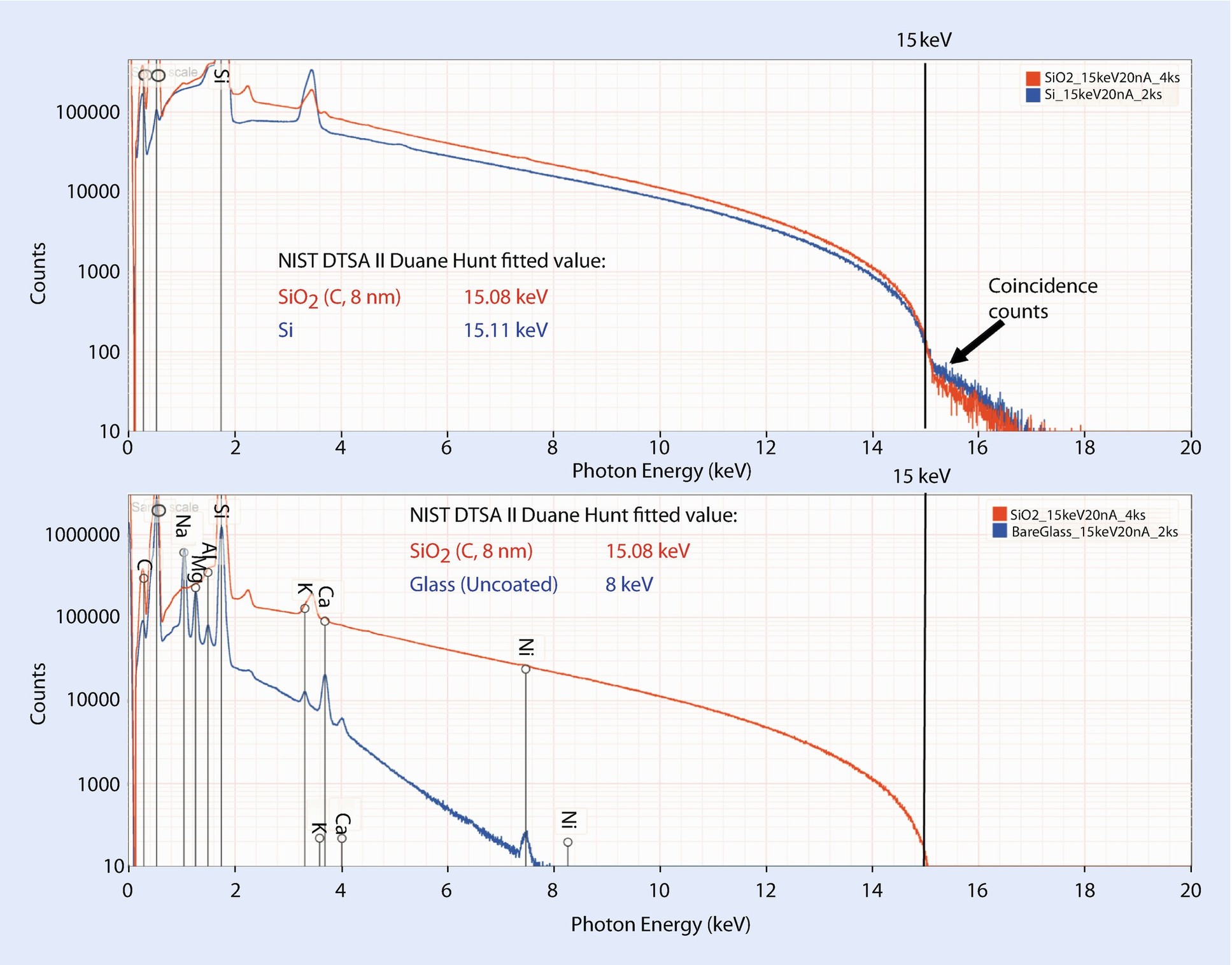
Effects of charging on the Duane–Hunt energy limit of the X-ray continuum: (upper) comparison of silicon and coated (C, 8 nm) SiO2 showing almost identical values; (lower) comparison of coated (C, 8 nm) SiO2 and uncoated glass showing significant depression of the Duane–Hunt limit due to charging

Choosing the Coating for Imaging Morphology

The ideal coating should be continuous and featureless so that it does not interfere with imaging the true fine-scale features of the specimen. Since the SE1 signal is such an important source of high resolution information, a material that has a high SE coefficient should be chosen. Because the SE1 signal originates within a thin surface layer that is a few nanometers in thickness, having this layer consist of a high atomic number material such as gold that has a high SE coefficient will increase the relative abundance of the high resolution SE1 signal, especially if the specimen consists of much lower atomic number materials, such as biological material. By using the thinnest possible coating, there is only a vanishingly small contribution to electron backscattering which would tend to degrade high resolution performance.

Although gold has a high SE coefficient, pure gold tends to form discontinuous islands whose structure can interfere with visualizing the desired specimen fine scale topographic structure. This island formation can be avoided by using alloys such as gold-palladium, or other pure metals, for example, chromium, platinum, or iridium, which can be deposited by plasma ion sputtering or ion beam sputtering. The elevated pressure in the plasma coater tends to randomize the paths followed by the sputtered atoms, reducing the directionality of the deposition and coating many re-entrant surfaces. For specimens which are thermally fragile, low deposition rates combined with specimen cooling can reduce the damage.

9.2 Radiation Damage

Certain materials are susceptible to radiation damage (“beam damage”) under energetic electron bombardment. “Soft” materials such as organic compounds are especially vulnerable to radiation damage, but damage can also be observed in “hard” materials such as minerals and ceramics, especially if water is present in the crystal structure, as is the case for hydrated minerals. Radiation damage can occur at all length scales, from macroscopic to nanoscale. Radiation damage may manifest itself as material decomposition in which mass is actually lost as a volatile gas, or the material may change density, either collapsing or swelling. On an atomic scale, atoms may be dislodged creating vacancies or interstitial atoms in the host lattice.

An example of radiation damage on a coarse scale is illustrated in ◘ Fig. 9.13, which shows a conductive double-sided sticky polymer tab of the type that is often used as a substrate for dispersing particles. This material was found to be extremely sensitive to electron bombardment. As the magnification was successively reduced in a series of 20-s scans, radiation damage in the form of collapse of the structure at the previous higher magnification scan was readily apparent after a single 20-s scan (20 keV and 10 nA). Note that when this tab is used as a direct support for particles, the susceptibility of the tab material to distortion due radiation damage can lead to unacceptable image drift. Instability in the position of the target particle occurs due to changes in the support tape immediately adjacent to the particle of interest where electrons strike, directly at the edges of the image raster and as a result of backscattering off the particle. Other support materials are less susceptible to radiation damage. ◘ Figure 9.14 shows a detail on a different conductive sticky tape material. After a much higher dose (15 min of bombardment at 20 keV and 10 nA), a much less significant collapse crater is seen to have formed. It is prudent to examine the behavior of the support materials under electron bombardment prior to use in a particle preparation.
../images/271173_4_En_9_Chapter/271173_4_En_9_Fig13_HTML.png
Fig. 9.13

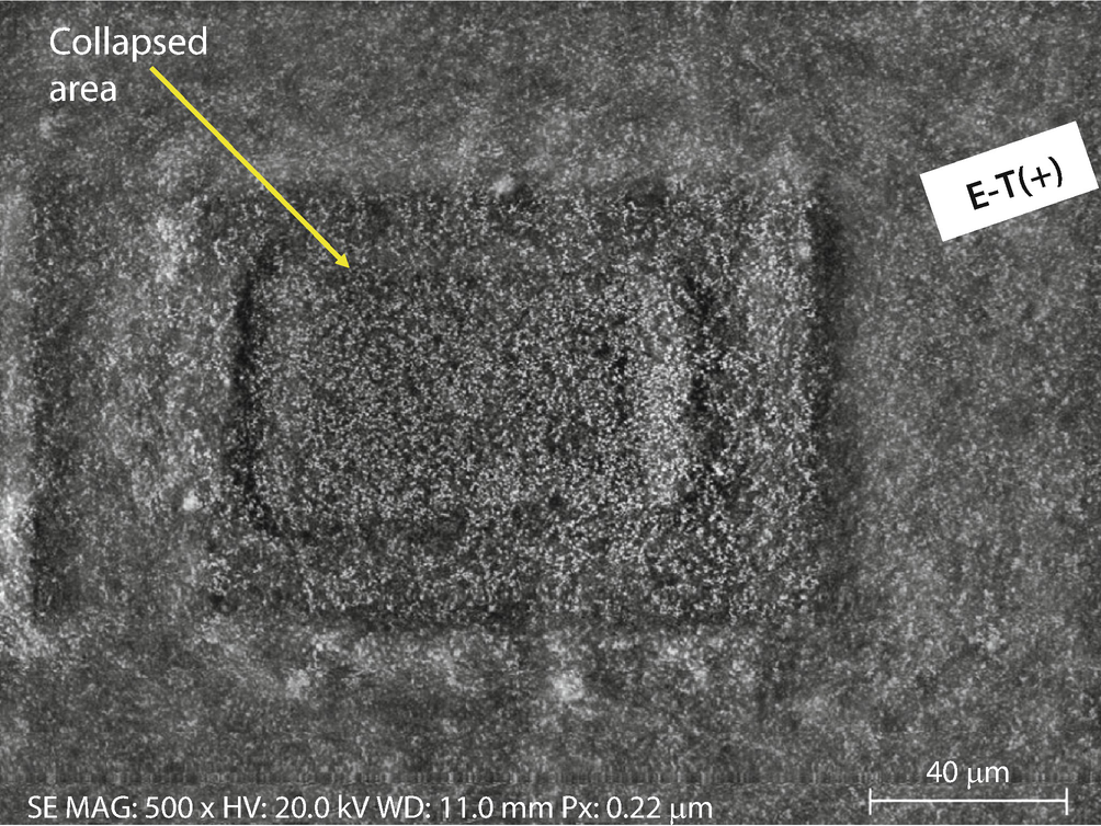
SEM Everhart–Thornley (positive bias) image of double-sticky conducting tab

../images/271173_4_En_9_Chapter/271173_4_En_9_Fig14_HTML.jpg
Fig. 9.14

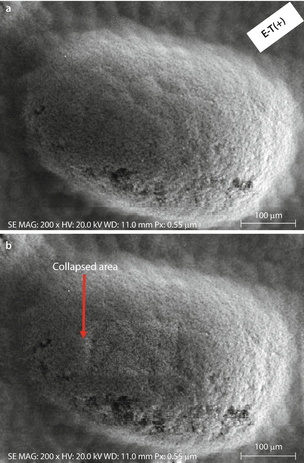
Conducting tape: a Initial image. b Image after a dose of 15 min exposure at higher magnification (20 keV and 10 nA); Everhart–Thornley (positive bias)

If radiation damage occurs and interferes with successful imaging of the structures of interest, the microscopist has several possible strategies:
  1. 1.
    Follow a minimum dose microscopy strategy.
    1. a.

      Radiation damage scales with dose. Use the lowest possible beam current and frame time consistent with establishing the visibility of the features of interest. It may be necessary to determine these parameters for establishing visibility for the particular specimen by operating initially on a portion of the specimen that can be sacrificed.

       
    2. b.

      Once optimum beam current and frame time have been established, the SEM can be focused and stigmated on an area adjacent to the features of interest, and the stage then translated to bring the area of interest into position. After the image is recorded using the shortest possible frame time consistent with establishing visibility, the beam should be blanked (ideally into a Faraday cup) to stop further electron bombardment while the stored image is examined before proceeding.


  2. 2.

    Change the beam energy

    Intuitively, it would seem logical to lower the beam energy to reduce radiation damage, and depending on the particular material and the exact mechanism of radiation damage, a lower beam energy may be useful. However, the energy deposited per unit volume actually increases significantly as the beam energy is lowered! From the Kanaya–Okayama range, the beam linear beam penetration scales approximately as E 0 1.67 so that the volume excited by the beam scales as (R K-O)3 or E 0 5. The energy deposited per unit volume scales as E 0/E 0 5 or 1/E 0 4. Thus, the volume density of energy deposition increases by a factor of 104 as the beam energy decreases from E 0 = 10 keV to E 0 = 1 keV. Raising the beam energy may actually be a better choice to minimize radiation damage.

     
  3. 3.

    Lower the specimen temperature

    Radiation damage mechanisms may be thermally sensitive. If a cold stage capable of achieving liquid nitrogen temperature or lower is available, radiation damage may be suppressed, especially if low temperature operation is combined with a minimum dose microscopy strategy.


9.3 Contamination

“Contamination” broadly refers to a class of phenomena observed in SEM images in which a foreign material is deposited on the specimen as a result of the electron beam bombardment. Contamination is a manifestation of radiation damage in which the material that undergoes radiation damage is unintentionally present, usually as a result of the original environment of the specimen or as a result of inadequate cleaning during preparation. Contamination typically arises from hydrocarbons that have been previously deposited on the specimen surface, usually inadvertently. Such compounds are very vulnerable to radiation damage. Hydrocarbons may “crack” under electron irradiation into gaseous components, leaving behind a deposit of elemental carbon. While the beam can interact with hydrocarbons present in the area being scanned, electron beam induced migration of hydrocarbons across the surface to actually increase the local contamination has been observed (Hren 1986). Sources of contamination can occur in the SEM itself. However, for a modern SEM that has been well maintained and for which scrupulous attention has been paid to degreasing and subsequently cleanly handling all specimens and stage components, contamination from the instrument itself should be negligible. Ideally, an instrument should be equipped with a vacuum airlock to minimize the exposure of the specimen chamber to laboratory air and possible contamination during sample exchange. A plasma cleaner that operates in the specimen airlock during the pump down cycle can greatly reduce specimen-related contamination by decomposing the hydrocarbons, provided the specimen itself is not damaged by the active oxygen plasma that is produced.

A typical observation of contamination is illustrated in ◘ Fig. 9.15a, where the SEM was first used to image an area at certain magnification and the magnification was subsequently reduced to scan a larger area. A “scan rectangle” is observed in the lower magnification image that corresponds to the area previously scanned at higher magnification. Within this scan rectangle, the SE coefficient has changed because of the deposition of a foreign material during electron bombardment, most likely a carbon-rich material which has a lower SE coefficient. Note that the contamination is most pronounced at the edge of the scanned field, where the beam is briefly held stationary before starting the next scanned line so that the greatest electron dose is applied along this edge.
../images/271173_4_En_9_Chapter/271173_4_En_9_Fig15_HTML.jpg
Fig. 9.15

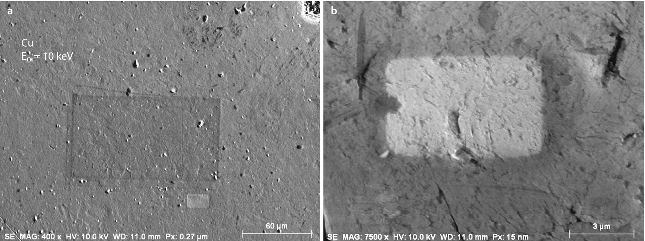
a Contamination area observed after a higher magnification scan; Everhart–Thornley (positive bias). The extent of the contamination is visible upon lowering the magnification of the scan, thus increasing the scanned area. b Etching of a surface contamination layer observed during imaging of an aluminum stub; Everhart–Thornley (positive bias); 10 keV and 10 nA

“Etching,” the opposite of contamination, can also occur (Hren 1986). An example is shown in ◘ Fig. 9.15b, where a bright scan rectangle is observed in an image of an aluminum stub after reducing the magnification following scanning for several minutes at higher magnification. In this case, the radiation damage has actually removed an overlayer of contamination on the specimen, revealing the underlying aluminum with its native oxide surface layer (~4 nm thick), which has an increased SE coefficient compared to the carbon-rich contamination layer.

Contamination is usually dose-dependent, so that the high dose necessary for high resolution microscopy, for example, a small scanned area (i.e., high magnification) with a high current density beam from a field emission gun, is likely to encounter contamination effects. This situation is illustrated in ◘ Fig. 9.16, which shows contamination in scanned areas on a patterned silicon sample used for dimensional metrology (Postek and Vladar 2014). The contamination in this case was so severe that it actually altered the apparent width of the measured features. To perform successful measurements, the authors developed an aggressive cleaning procedure that minimized contamination effects for this class of specimens. Their strategy may prove useful for other materials as well (Postek and Vladar 2014).
../images/271173_4_En_9_Chapter/271173_4_En_9_Fig16_HTML.png
Fig. 9.16

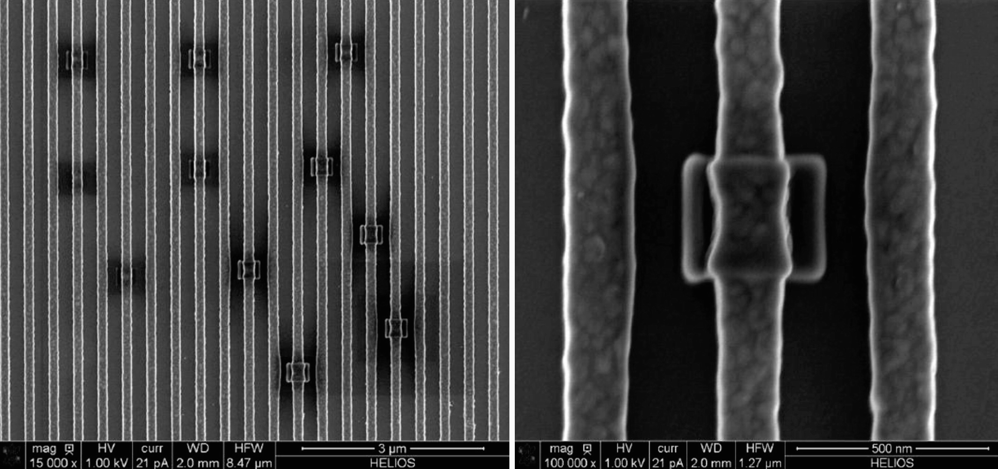
Contamination observed during dimensional measurements performed under high resolution conditions on a patterned silicon substrate (Postek and Vladar 2014). Note broadening of the structure (right) due to contamination

9.4 Moiré Effects: Imaging What Isn’t Actually There

An SEM image appears to be continuous, but it is constructed as a regular repeating two-dimensional pattern of pixels. Thus, the viewer is effectively looking at the specimen through a two-dimensional periodic grid, and if the specimen itself has a structure that has a regularly repeating pattern, then a moiré pattern of fringes can form between the two patterns. The form of the moiré interference fringes depends on the spacing and orientation of the specimen periodic pattern and the scan pattern. Moiré patterns are maximized when the spatial frequencies of the two patterns are similar or an integer multiple of each other (i.e., they are commensurate). The formation of moiré patterns is illustrated in ◘ Fig. 9.17, which shows various etched patterns in the NIST RM 8820 magnification calibration artifact. The structures have different spacings in each of the fields viewed at the lowest magnification so that different moiré patterns are observed in each field. As the magnification is increased the scan field decreases in size so that the SEM pattern changes its periodicity (spatial frequency), causing the moiré pattern to change. Finally, at sufficiently high magnification, the specimen periodic structure becomes sufficiently different from the scan pattern that the moiré fringes are lost.
../images/271173_4_En_9_Chapter/271173_4_En_9_Fig17_HTML.jpg
Fig. 9.17

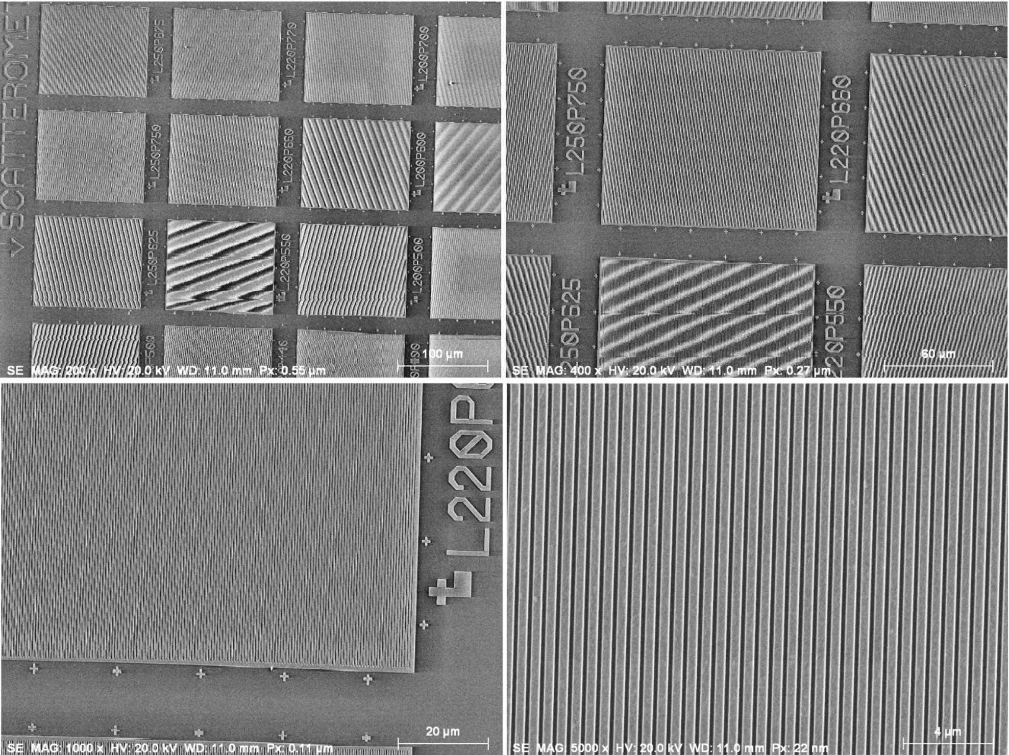
Moiré fringe effects observed for the periodic structures in NIST RM 8820 (magnification calibration artifact). Note the different moiré patterns in the different calibration regions; Everhart–Thornley (positive bias) detector

Moiré effects can be very subtle. The periodic bright flares at fine edges, as seen in ◘ Fig. 9.18, are moiré patterns created when the fine scale structure approaches the periodicity of the scan grid.
../images/271173_4_En_9_Chapter/271173_4_En_9_Fig18_HTML.png
Fig. 9.18

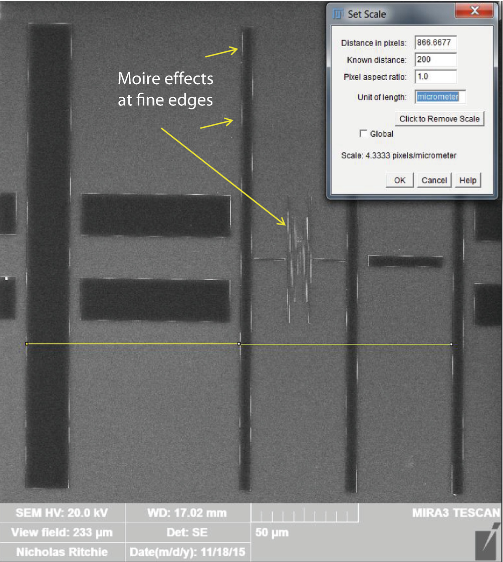
Moiré effects seen as periodic bright flares at the edge of fine structures in NIST RM 8820 (magnification calibration artifact); Everhart–Thornley (positive bias) detector

To avoid interpreting moiré effects as real structures, the relative position and/or rotation of the specimen and the scan grid should be changed. A real structure will be preserved by such an action, while the moiré pattern will change.

Creative Commons

Open Access This chapter is licensed under the terms of the Creative Commons Attribution-NonCommercial 2.5 International License (http://creativecommons.org/licenses/by-nc/2.5/), which permits any noncommercial use, sharing, adaptation, distribution and reproduction in any medium or format, as long as you give appropriate credit to the original author(s) and the source, provide a link to the Creative Commons license and indicate if changes were made.

The images or other third party material in this chapter are included in the chapter's Creative Commons license, unless indicated otherwise in a credit line to the material. If material is not included in the chapter's Creative Commons license and your intended use is not permitted by statutory regulation or exceeds the permitted use, you will need to obtain permission directly from the copyright holder.