6
Reversible Computing and Quantum Computing
Reversible computing was introduced in Chapter 2 with regard to the link established between information and dissipation. It was also presented as a technique for implementing adiabatic principles. This chapter is a general introduction to reversible computing, allowing us to define the different reversible logic gate families, as well as the basic elements for synthesizing reversible logic architectures. Reversible computing makes extensive use of group theory, of which a few reminders will be given in the different sections of this chapter. The subject may seem complicated, but it will also be new for many readers, as this approach is neither well known nor taught often. The reader will no doubt find the mathematical richness of these concepts introduced, as well as by the contribution that group theory has made to synthesizing reversible logic architectures, very useful. This chapter builds on the very expansive book by Alexis De Vos [DE 10].
6.1. The basis for reversible computing
6.1.1. Introduction
The current computers/calculators are reversible. The result of a calculation is known when the inputs are defined, but, in general, the output values are not enough to find the input values. Let us use the example of a simple adder. As the output A + B is given, there are various combinations with the values A and B which give the same result. In order to find the input values, the calculator only needs to have an additional output, A – B, for example. Therefore, the calculator is reversible.
This definition can be applied in the same way to the logic gates, with the gate considered a binary elementary calculator. An AND gate is irreversible because, as the output is zero, there are three possible input combinations: (0,0), (0,1), (1,0). The inverter, on the other hand, is reversible. It is not difficult to understand that a Boolean function is reversible when a bijection is defined between the different possible input combinations and the different corresponding outputs. The result is that the reversible gates must have the two following properties:
- 1) The number of outputs is equal to the amount of inputs.
- 2) For two different input words, the output words are different.
The word is a given combination of the values “0” and “1”. Figure 6.1 gives two examples of reversible gates and one example of an irreversible gate.

Figure 6.1. Reversible and irreversible gates
When the gate is reversible, the outputs are one of the possible permutations of the inputs. The number of inputs equal to the amount of outputs is the gate width w. The number of possible words at input or output is 2w. In Figure 6.1, the reader will easily be able to recognize the identity (gate b) and the parallel placing of a function AND and a function OR (gate c). Gate c shows that having the same amount of inputs and outputs is not enough to be reversible. Finally, every reversible gate has an inverse gate. We can keep the same truth table, but permutate the inputs and outputs. The product of a gate and its inverse is the identity.
6.1.2. Group structure of reversible gates
Let us recall the properties of a group. In reversible computing, the operation consists of cascading the gates. We need to ensure that the following properties are present:
- – the group is closed, meaning a ○ b belongs to the group;
- – the operation is associative, meaning (a ○ b) ○ c = a ○ (b○ c );
- – the group has a unit element I such that: a ○ i = a ;
- – every a element has an inverse a−1, such that a ○ a−1 = i.
The amount of elements is the order of the group. The last property explains the natural link between reversible gates and group theory.
The group will, therefore, be a set of gates of a given width. If all operations are possible, the amount of possible functions or gates is 2W. In fact, 2W is the number of possible words, in the binary sense of the terms, for a gate’s inputs. Reversibility implies that the possible outputs are all of the possible permutations corresponding to a given word. Let us use the example of gates with a width of 2 and now we construct a reversible gate based on the list of all possible input combinations.
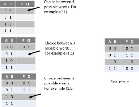
Figure 6.2. Constructing a reversible gate with a width of 2
In this example, there are a total of 4 possible gates. For a width of 3, the amount of possible gates would be 40,320. The order of the group rapidly increases with the width.
There is obviously a unit element that exists. The outputs are identical to the inputs. The existence of an inverse gate for each of the group’s gates is just trivial because it is enough to choose the gate that enables a return to the input among the possible gates. This choice is possible and unique, given the permutation definitions.
6.1.3. Conservative gates, linearity and affinity
The reversible gates may be conservative, linear or affine. These properties allow sub-groups to be defined.
6.1.3.1. Conservative gates
They form a sub-group with the following property: the number of “1” at output is equal to the number of “1” at input.
6.1.3.2. Linear gates
The definition of this is the same as that for classic logic. A reversible logic gate is linear if each of the outputs is a linear Boolean function of the inputs. Each output can, therefore, be written with coefficients Ci that are zero or equal to one in the following form, which only uses an exclusive OR function:

An example of a linear gate is the gate defined by:

It can also be defined by the matrix:

6.1.3.3. Affine linear gates
The definition for this is the same as for classic logic. The Reed–Muller development can also contain constants. An example of a linear gate is the gate defined by:

In this case,

Here, we refer to a remarkable theorem of reversible Boolean logic: a reversible gate is universal (meaning that each function can be constructed by combining a certain number of gates of this same type) if and only if it is not an affine linear. Note that synthesizing a function in reversible logic cannot be done by applying an output to various inputs. An explanation for this fundamental rule called the “no fan-out” rule will be given in 6.1.6. The vast majority of reversible gates are not affined linear, and, therefore, they can be considered potential universal gates.
6.1.4. Exchange gates
This is a sub-group that is particularly significant in reversible logic. The definition is quite restricting because each output must be one of the inputs. For example, the following gate is an exchange gate:

The graphical representation is given as follows:

The truth table is presented in Table 6.1.
Table 6.1. The truth table
| A | B | C | P | Q | R |
| 0 | 0 | 0 | 0 | 0 | 0 |
| 0 | 0 | 1 | 0 | 0 | 1 |
| 0 | 1 | 0 | 1 | 0 | 0 |
| 0 | 1 | 1 | 1 | 0 | 1 |
| 1 | 0 | 0 | 0 | 1 | 0 |
| 1 | 0 | 1 | 0 | 1 | 1 |
| 1 | 1 | 0 | 1 | 1 | 0 |
| 1 | 1 | 1 | 1 | 1 | 1 |
This function can be represented in two possible ways: the first is a column permutation and the second is a line permutation. They lead to two different matrices:
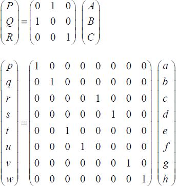
The second matrix is less obvious and is in fact the matrix associated with the permutation corresponding to the reversible function. It is constructed based on the truth table. The elements (a,b,c,…) and (p,q,r,…) are the possible words for input and output.
By using the cycle notation of group theory, it is written (3,5) (4,6), which means that the third line becomes the fifth line, and that the fourth line becomes the sixth line. The others remain unchanged.
Table 6.2. The truth table
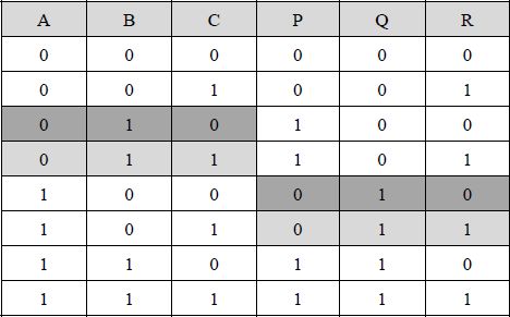
There are two possible permutations: line permutation or column permutation.
When only two inputs are exchanged, the exchange gates are called “swap gates” and they make up a particular set, which is not a group. In fact, cascading of the two swap gates in a series is not necessarily a swap gate.
An affined exchanger is the exclusive OR of an exchanger and a constant. For example:
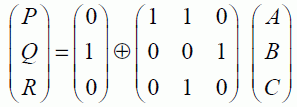
Finally, note that the cascading operation is not generally commutative. The writing order for the invertible functions is, therefore, very important.
6.1.5. Control gates
This is the last reversible sub-group that we will introduce. This is the most important sub-group as the control gates are mainly used in synthesis. Figure 6.3 represents a control gate in general.
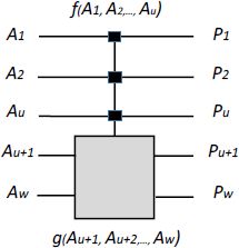
Figure 6.3. Control gate
- – There are two types of inputs: the control inputs in the number u and the controlled inputs in the number w–u. When the function f of the control inputs is “0”, the outputs are all a simple copy of the inputs. When the function of the control inputs is “1”, the control inputs are transmitted, but the controlled outputs are the outputs of a reversible function g for the controlled inputs w–u.
- – This set effectively has a group structure and can be considered a particular sub-group of the reversible gates group. We will satisfy ourselves by graphically showing that cascading two control gates is also a control gate.
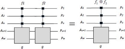
Figure 6.4. Cascading two control gates
When the two functions are performed simultaneously, the output of the reversible cascaded gates is really a copy of the inputs. The command function to apply is the exclusive OR. The reader is also encouraged to ensure that the control gate’s inverse is the control gate itself.
When the command function is an AND function, a black circle is used instead of a black rectangle. When the inverse variable is used in the AND function, the circle is white. These conventions are specific to the reversible logic.
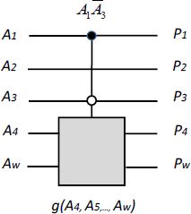
Figure 6.5. The conventions of reversible logic for a control gate
Now, we are going to introduce some well-known gates: the control inverter, the Toffoli gate, the Feynman gate and the Fredkin gate:
- – The control inverter:
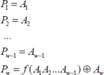
The function g is reduced to a single-variable function: the transmitter or the inverter is the only possibility.
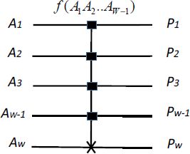
Figure 6.6. Control inverter
The logical functions can be written as follows:
- – The Toffoli gate:
The function g is the inverter and the control function is an AND function. The inverter function is represented by a cross.
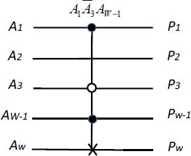
Figure 6.7. Toffoli gate
- – Feynman gate:
This is a particular Toffoli gate, as the control function depends only on one variable.
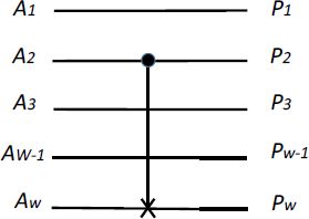
Figure 6.8. Feynman gate
- – Fredkin gate:
This is a “swap gate” with an AND function as a control function.

Figure 6.9. Fredkin gate
6.1.6. Two basic theorems: “no fan-out” and “no cloning”
Reversible logic imposes some very specific constraints, which are not very intuitive for those accustomed to classic logic. The first is the prohibition of connecting a reversible gate output to more than one gate input. This is called the “no fan-out” theorem. The second is the prohibition of duplicating an output by a simple cabling, which would be a particular way of breaching the previous principle. In order to establish this theorem, we must consider separating a signal into two identical signals like a particular gate. The first two diagrams are not possible in reversible logic because a reversible gate must have the same number of inputs and outputs. The one-input Feynman gate, on the other hand, is a possible implementation. A supplementary signal with a constant “0” value has been added to the input.

Figure 6.10. Duplicating a signal and a fan-out
The consequence of these rules is that the structure of a system performing a reversible function can only be a cascading structure of gates of the same width. This topological “simplicity” is to be compared with the complexity of an irreversible system authorizing duplications and “fan-outs”.
6.2. A few elements for synthesizing a function
6.2.1. The problem and constraints on synthesis
To synthesize a function is to conceive a logic gate architecture that performs a given logical function. The previous considerations have shown that many gate families can be used to do this and that only the affine linear gates were outlawed. However, all of the solutions are not equivalent and there are some criteria which need to be defined for optimization.
Two reversible logic criteria may be found: the cost as measured by the amount of elementary gates and the depth of the logic. The depth of the logic means the maximum number of stages put into a series. Thus, we understand that, by reducing the number of gates, they are reducing the cost and the dissipation. Reducing the depth of the logic means that the circuit speed will be increased.
Now, there is another criterion introduced (the cost expressed as the number of switches), but for that we need to have a minimum knowledge of the technology used. The way in which the cost in the number of gates is to be evaluated is the subject of many debates, but there is a simple way which consists of assigning a cost of absolute zero to an exchange gate and a cost of 1 to a control gate. This counting method assumes that the exchange gates are simpler to design.
Before the synthesis, there are two possible cases: the logical function is reversible or irreversible. In the case where the function is reversible, methods inspired by group theory will be used. In the case where the logical function is irreversible, the first step is to transform it into a reversible function. We will present a few introductory elements for synthesizing reversible functions.
6.2.2. Synthesizing a reversible function
Sylow circuits give an initial idea of what methods are possible. Figure 6.11 represents a Sylow cascade with a dimension of 4 and a width decreasing from left to right.
This pattern was inspired by a control inverter and shows how to cascade gates with an “active” decreasing width. In fact, the total width remains the same in the chain, as the reversible logic imposes, but the “active” part is of a decreasing width.
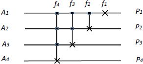
Figure 6.11. Sylow cascade
These synthesis methods appeal to the group’s properties that we will develop in this chapter. Using the “cosets” and “double cosets” allows an efficient synthesis algorithm [DE 10] to be developed. These are the group’s partitions considered to be in the order G in the G/H sub-groups of the order H. Therefore, it is possible to break down a reversible function in a cascade of controlled inverters and “twin circuits”.
The twin circuit is represented in Figure 6.12. The twin circuits with a given dimensions have the structure of thee sub-group from the reversible gate group with the same dimensions.
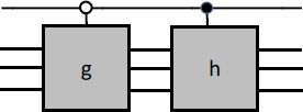
Figure 6.12. The “twin circuit”
This circuit performs the reversible function h if the command is “1” and g if the command is “0”.
Thus, it has been shown that every reversible gate with the width w can be performed using the following cascade:
- – a “twin gate” with the width w–1;
- – a controlled inverter;
- – a second “twin gate” with the width w–1.
This process can continue by decreasing the block width each time.

Figure 6.13. Synthesis of a reversible function
The reversible functions with an inferior width are determined by the algorithm and are different too the initial function. This method is very efficient, but it is not the only one.
Another method allows each step to be broken down into an irreversible function in a cascade with three functions:
- – a controlled inverter with the width w–11;
- – a “twin gate”;
- – a second controlled inverter with the width w–1.
The total synthesis of the circuit is done according too the steps shown in Figure 6.14. The width of the functions decreases with every step, which enables the final synthesis. The algorithm is actually simple enough, but it has not been described in detail in this chapter, which is just a simple introduction to reversible logic. However, it is cited in [DDE 10].
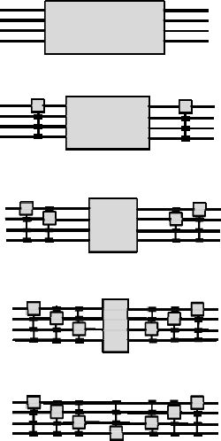
Figure 6.14. The synthesis steps
6.2.3. Synthesizing an irreversible function
In practice, this is the most frequent problem, as the logical functions are generally defined in irreversible logic. Let us use the example of the binary adder with N bits.
In order to use the synthesis given in the previous section, it is first necessary to understand how it is possible to transform an irreversible function into a reversible function. This exercise will introduce the notion of “garbage” in reversible computing and of overhead of gate numbers, which is often quite rightly presented as a major drawback.
Let us use another example: the simple copying of a Boolean variable. As we have already seen, it is not possible to physically duplicate the signal as it would mean inserting an irreversible gate into a reversible gate chain. A simple solution to this is to add the function into the truth table by copying a supplementary input F.
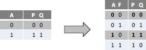
Figure 6.15. The reversible copy
So, placing F at “0” is enough for the outputs P and Q to be two copies of A. The global truth table is really that of a reversible gate.
A second example is that of reversible or irreversible interpretation of a controlled inverter. The control function F is assumed to be irreversible. A controlled inverter can “board” this function. A supplementary input U must be added. Therefore, the logical equations are:

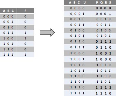
Figure 6.16. Controlled inverter boarding an irreversible function
The useful output is the output S, while the outputs P, Q and R are not used. These are called “garbage”. The total reversible function can then be synthesized by following the principles outlined earlier.
Another example is that of the majority gate. Output is equal to zero if the majority of inputs are “0”, and equal to “1” otherwise. This is a reversible function that we will board onto a reversible function by adding two supplementary inputs. Figure 6.17 describes the two truth tables. There are many ways of completing the initial table in order to obtain a reversible table. The simplest solutions may be chosen because the supplementary variables are not used. Then, the synthesis can be done by cascading the controlled inverters, all while following the synthesis algorithm.
6.2.4. The adder example
Although this is a textbook case, it can also be a real problem because addition is the basic operation in binary calculation. It is an irreversible operation. Ai and Bi are the input bits, Ci is the carry-in bit and Ci+1 is the carry-out bit. The logical equations written for Si are:
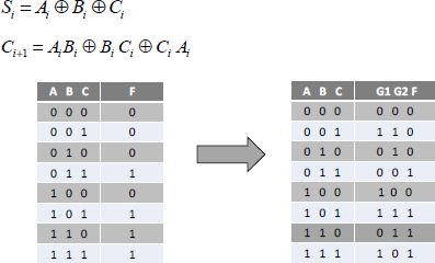
Figure 6.17. Example of a majority gate
The truth table can, therefore, be extended, as shown in Figure 6.18.

Figure 6.18. Truth table of a reversible adder
In the first step, two outputs are added so that the same word does not appear many times, which would be contrary to the reversibility. A supplementary column in this case is enough. Then, a column is added to the input so that the number of outputs is equal to the number of inputs. The two supplementary variables that are part of the “garbage” are G1 and G2. They are simply Bi and Ci.
The general algorithm leads to 2w–1 or 7 control gates to carry out the synthesis. The control functions as determined by the algorithm are:
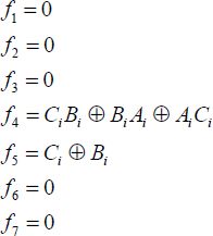
The pattern can be reduced to two control gates because five control functions are at absolute zero. It is shown in Figure 6.19.

Figure 6.19. Synthesis of a reversible binary adder
Classically, these one-bit adders can be assembled by forming an adder with any number of bits, as shown in Figure 6.20.
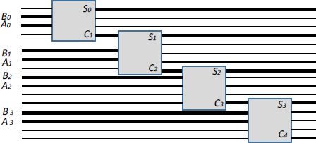
Figure 6.20. A 4-bit reversible adder
The really useful signal lines are marked in bold in the figure. This example shows the overhead off logic gates when the reversible solution is chosen.
6.2.5. Hardware implementation of reversible gates
The material implementations of gates are only pertinent if they are compatible with the adiabatic principle of optimal capacitor charge and discharge. They are inspired by the following functional architectures. The controlled inverters are taken as examples.
6.2.5.1 . Inverter controlled by a single control bit
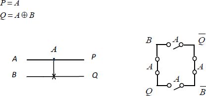
Figure 6.21. Inverter controlled by a single control bit
The switches are commanded by the variable A. They are in the position shown in the diagram when the control variable, A in the occurrence, has the value of “0”. They change position when the variable A has the value “1”. When A is at “0”; the output Q is then connected to B. If A is at “1”, the output Q is connected to  . The output P is connected to A.
6.2.5.2. Inverter controlled by two control bits
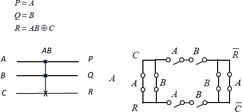
Figure 6.22. Inverter controlled by two inputs
In CMOS technology, the switches are either NMOS or PMOS. However, in a more beneficial way, transmission gates are made by putting the PMOS and NMOS parallel, which are commanded by a signal and the complementary signal. The electrical properties are, therefore, improved and closer to those of the ideal switch.
In order to attain the aims of low consumption, the reversible gates must implement the adiabatic principle outlined in Chapter 2. This principle leads to giving the signals a quasi-ideal form of ascending and descending ramps (as studied in Chapter 2). Alexis De Vos proposed giving the signals a triangular form (as shown in Figure 6.23). Two constant logical states are shown, one in the “on” state and another in the “off” state. The third signal moves from the “off” state to the “on” state.
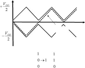
Figure 6.23. The signals in reversible adiabatic logic
Let us now consider a reversible circuit with two inputs v and w as depicted Figure 6.24. One input stays in the “on” state, while the second moves from the “off” state to the “on” state. We assume that the “off” state corresponds to the negative values and the “on” state to the positive values. Figure 6.23 shows a possible configuration. It should be carefully noted that a signal that does not change the state is not electrically constant, as it also changes linearly during the transition and then returns to its original level.

Figure 6.24. Adiabatic command of a reversible circuit
The electrical connection between input and output is made by a transmission gate formed by putting the NMOS and PMOS in parallel and commanded by complementary signals. This device commanded by a signal “1” is always moving, except during the time interval between which the command voltage w is less than the minimum v +VT and - v + VT . The variable VT is the common value of the two thresholds of the transmission gate, which are supposed identical. Calculating the dissipated energy (a rather long, but simple calculation) leads to the following result. This section does not describe this in detail:
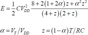
The time T is the rise time of the ramp when the signal changes and R is the value assumed to be constant for the transmission gate’s resistance. The two extreme cases are the following:
- – ramp rise time is much lower than RC:

- – ramp rise time is much greater than RC:

In absolute terms, applying the adiabatic principle to perform the reversible gates in CMOS technology collides with the threshold voltage value. This voltage cannot be very weaker due to the sub-threshold current. This restriction shows that, in every case, whether reversible or not, the trade-off between static and dynamic power counters a very significant dissipation reduction. This result has already been proven in the quasi-adiabatic pipeline.
6.3. Reversible computing and quantum computing
This last section is a short introduction to quantum computing because there are strong links between it and the reversible logic.
6.3.1. Principles of quantum computing
Quantum computing, which was introduced in the 1980s by Feynman and Bennett, is based on two main ideas. The first is the electronic miniaturization that leads to changing the functioning laws of electronic devices, going from the classical domain to the quantum domain. The second is that computers are still based on the Turing model, but this model becomes probabilistic. The concepts of reversible logic are very useful for implementing these new computers. Quantum gates were then introduced.
The bit is the support for the information in classical logic (either reversible or irreversible). It is either in the “off” state or the “on” state. In quantum computing, the support for the information is the qubit, which is a linear superposition of the possible states noted as  , for example, the two states corresponding to two energy levels or two spin orientations or two polarizations. The qubit is a quantum state written as:

Coefficients a and b are any complex amounts that obey the following condition:

This condition is called the normalization condition.
In quantum computing, the qubit represents both the information and the physical state that brings about the information, at the same time. In classic computing, the two concepts are separated and a logic state is carried out by a large amount of physical states. An atom with two states, one fundamental and another excited, for example, can represent a qubit. An external perturbation (interaction with a photon) can make the system move from one state to another. A measuring operation in the quantum mechanics sense allows the state of the atom to be decided, and, therefore, for the state  or
or  to be read.
A classical register is a set of n bits, written for instance as (1, 0, 1), for n equal to three. A n quantum register is a qubits set in a space of 2n dimensions. It is written as:

The qubits can be transformed by the logical operators that can be represented by the matrices with the dimension 2n times 2n by defining the actions on the basic vectors. Either these operations or the matrices will be assumed to be unitary, meaning that the matrix product by its conjugated transposition is the matrix unit.
Reversible computing makes use of invertible matrices with coefficients 0 or 1. Quantum computing makes use of matrices with any complex coefficient with a unitary property, because a logical operation is the evolution of the physical state of the qubits system in question. It must be associated with a unitary evolution operator such as that imposed by quantum mechanics. The normalization condition must also be fulfilled. These matrices form a Lie group in the order of n. The matrices of reversible computing are a sub-group of this group, although quantum computing can be considered a generalized version of reversible computing.
6.3.2. Entanglement
This notion is very specific to quantum computing and is not very intuitive. Before defining it, let us go back to classical computing and we will see how we can turn a one-bit system into a two-bit system. The two states of the one-bit system are considered as two vectors in a discrete space of two dimensions. These two vectors are:

Due to a tensor product, it is possible to construct a two-bit space, such as:

It is then easy to show that all the other vectors in the two-bit space can be obtained using the tensor product. Note that the operation is not commutative. Therefore, it can be said that the states are separable.
This property is no longer verified in quantum computing and the states obtained by tensor product represent only a small part of the possible states. The inseparable states are said to be entangled. The vector corresponding to two qubits is generally written as:

It is not necessarily written in the form of a two-state tensor product, each of which corresponds to one qubit. Below is an example of an entangled state:

This qubit can also be written as:

It is not possible to break this vector down into a tensor product. In fact, if that were the case, the two qubits would need to verify the below:
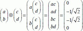
There is no solution to this four-equation system. The entangled states of a quantum register are, therefore, the most numerous states and carry more information than the constitutive qubits.
The basic vectors of a quantum register are noted as 
 , or, in a more compact way,
  by taking the numbers of the associated decimals.
6.3.3. A few examples of quantum gates
Let us place a qubit in a space. A useful quantum operator is defined as the square root of the inverter. The inverter v is naturally defined as exchanging the states “0” and “1”. This operator σ must be unitary and verify: σ2 = v. It is just easy to find that the associated matrix is:

Therefore, it can be verified that the inverse is the transposed matrix and that the squared matrix is equal to the inverter:
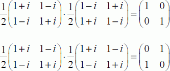
Thus, the two properties are established. The four matrices σ, v, σ2, φ make up a group of the order 4, the matrix φ being the matrix unit. This group is isomorphic to the cyclical group in the order 4.
Now, let us place it in the space corresponding to two qubits. The operators are represented by the 4× 4 matrices. The square root matrix is, therefore, defined as:

The following property is also verified:

If we now make the set made up of σ and the two matrices a and b, we obtain a group of the order 192. This property, that is difficult to establish, is not demonstrated in this introduction. The two matrices a and b are the two usual operators.

A complete quantum adder is shown in Figure 6.25. It uses the square root and the controlled inverter in the same way as in classical reversible computing.

Figure 6.25. Quantum adder
This last example illustrates a more general theorem: every quantum gate can be broken down into a cascade of uncontrolled qubits and gates controlled by a single qubit.
6.3.4. The example of Grover’s algorithm
In summary, quantum computing has points in common with reversible computing, especially when we think of descriptive mathematical tools and synthesis methods. However, it is fundamentally different because it does not manipulate “0” and “1” matrix elements like reversible computing, but uses more complex matrices. In this way, it is more akin to analogue computing.
We can understand the power of quantum computing when they consider reversible Boolean computing to be a restriction on quantum computing. A quantum circuit somehow simultaneously performs all the calculations corresponding to all the possible values of input variables, including the particular Boolean values. This property is often portrayed as a type of generic parallelism.
In order to illustrate this property, which is a huge part of quantum computing, let us use the example of Grover’s algorithm, the aim of which is to find an element in an unordered database. This database could be, for example, the list of N telephone numbers with the names of the associated subscribers in the alphabetical order. The aim is to find the name of the subscriber corresponding to a given telephone number as quickly as possible.
In classical computing, we need approximately N/2 tries to find the subscriber. In quantum computing, this number is reduced to  with an error probability of 1/N. The principle is to apply a series of operations to a quantum register representing the data. The final state converges toward the solution to the problem. An output register contains the solution to the problem at the end of the sequence.
In order to find this operation series, which is far from being intuitive, it is necessary to define the two operators (Sψ and O), which are called Hadamard’s operator and the oracle operator, respectively.
The N inputs are considered the N basic vectors, noted as  in an input quantum register. Let us call
  the basic vector corresponding to the required telephone number. The function f(x) associates each
  with the value 0 if
  is different from
  and with the value 1 if
  is equal to
  . The output register is, in two dimensions, corresponding to whether the function has been performed or not. The output qubits are noted as
  and the basic vectors are
  .
.
The quantum transformation oracle acting on the two input and output registers is defined by:

Hadamard’s operator applied to the input register’s basic vectors is defined by:

The notation xz actually represents the sum  of the binary decomposition coefficients associated with the basic vectors
  .
.
Now, let us assume that the output register with one qubit is placed in the state:

The quantum oracle operator applied to a basic vector gives the following result:

Finally, we define the operators S0 and Sψ as follows:
The operator S0 when applied to a basic vector changes its sign, except for  . The operator Sψ is defined by:

Grover’s operator G is then defined by:

Note that the oracle operator is the equivalent of a basic element exam in classic computing. The difference is in fact that the oracle is not applied to a basic vector, but to a state made by linear superposition of all the basic vectors constituting quantum parallelism.
The algorithm can be summarized as follows:
- – preparing the data by defining the input state as a uniform linear superposition of input vectors;
- – applying Grover’s transformation
 times;
 - – measuring the most probable output state. The solution to the problem is then found to have an error probability of 1/N.
A thorough demonstration of this algorithm’s convergence is outside the framework of this book. We will satisfy ourselves with a geometric explanation. The vector  is the solution to the problem. The orthogonal vector to this vector is
  . The initial vector can be broken down as follows:

This expression is also written with 

Those readers familiar with operations in vector spaces will be able to easily verify that applying the oracle is equivalent to a symmetry against the axis  . Those readers will also be able to easily verify that applying Sψ is equivalent to a symmetry against
  . In absolute terms, Grover’s transformation reconciles the
  state, according to an angle θ rotation. The new state according to the k applications of the transformation is written as:

The gap between  is minor, because
  even if N is high,
Notice that the final state is not necessarily  and, therefore, that there is a weak probability 1N of making a mistake in the final measurement. Quantum computing allows this example to move from N/2 iterations to
  iterations, which procures a significant gain when the basis has a large amount of elements.
This gain is possible, on the condition that the coherence of the state made up of linear superpositions of basic vectors is conserved during the calculation. Physical interactions with the environment can actually contain the circuit’s vector state in order to project the state into a more restricted space. In practice, we must devise physical components capable of not only performing quantum gate operations, but also restricting the interactions with the environment and keeping the coherence time compatible with the computing time. This difficulty has still not been resolved today, even if considerable gains have been made.
There is a second difficulty, which is linked to the analogue nature of the computing. In order to resolve a problem, we must actually transform it into a particular algorithm compatible with the operations that the quantum gates can perform. There have been two general algorithms designed since quantum computing was introduced. One of them is Shor’s algorithm that enables us to write a number as a product of prime numbers and Groves’ algorithm that enables an element to be found in an unordered database. This limited number shows how difficult the method is.
Furthermore, these two algorithms are very important for obtaining reasonable computing times in coding and searching problems in the database, the two basic problems in digital technologies. In both of these cases, the contribution that quantum computing has made is undeniable. In conclusion, quantum circuits could be used as the co-processors to more conventional computers in the distant future.