3
Applications of the WCIP Method to Frequency Selective Surfaces (FSS)
The iterative method Wave Concept Iterative Procedure (WCIP) as applied to planar structures is set out. Based upon a formulation in transverse waves and wave gathering at interface level, the solution to the electromagnetic issue is obtained through using an iterative procedure. The use of bounded operators within the iterative method makes convergence a certainty, independently of the planar circuit on the frequency selective surfaces (FSS) interfaces. Diodes, inserted to obtain an active FSS structure, as well as gaps and short-circuits have the role of both controlling and adjusting the characteristics of FSS diffractions. Within Frequency Selective Surfaces (FSSs) controlled by diodes, the latter are considered surface impedances within the iterative method and its two-port network may thus be established. The WCIP method, switches between the spatial domain and the modal domain via the Fast Modal Transform (FMT) – to resolve the electromagnetic issue. The FMT based upon the algorithm of the bi-dimensional FFT (Fast Fourier Transform) then allows significant savings both in terms of computational time and memory space. Several FSS structures have been analyzed by using the WCIP method. The results obtained are compared with the measurement results and the simulation from the works in the field, and an overall consensus of findings is then evident.
3.1. Introduction
Frequency Selective Surfaces (FSS) are largely used as low-pass filters, high-pass filters, notch filters, or band-pass filters [GAO 05, MON 05]. Charged Frequency Selective Surfaces (FSSs) make flexibility within the adjustment of transmission characteristics possible. However, electronically-adjusted, or so-called active FSSs, are very significant in compensating for manufacturing errors and for the adaptation of the FSS filters to frequency variations in the operation of wireless communication systems [MAR 05, MAR 05]. The use of short-circuits within FSS dielectric rings ensures precise resonance frequency control [MAR 01] by varying the position of inserted short-circuits. For multi-band and large-band, multi-ring FSSs [VOY 06, AUB 06, QUI 06] and multilayer plated FSSs are used [UCA 08, SON 08, ERD 08]. It is possible to create dual-polarized FSSs when a careful decision upon FSS circuit is made.
Several methods have been used to resolve such problems. Amongst these methods, the Finite-Difference-Time-Domain (FDTD) method, the Transmission Line Matrix (TLM), the immittance method in conjunction with the method of moments [CAM 02, GOM 02] are currently adopted. Nevertheless, the tendency towards “Full Wave” simulations of entire microwave systems is expanding rapidly [WAN 03, BAU 03]. Indeed, this approach gives more accurate results, when compared with multi-block modeling and assembly with a series of element behaviors, making up a comprehensive circuit, where the linking of elements is simply neglected. The iterative “Wave Concept Iterative Procedure” (WCIP) method, developed for several years within the electronics laboratory LEN7 in Toulouse France, responds to these demands and offers an efficient and general solution for planar structures, when the analysis revolves around transverse waves. It also sets out a solution for all types of structure if volumes waves are used.
The iterative WCIP method considers the FSS structure as a form of periodic structure. The analysis of such a structure is reduced to that of the unit cell, indeed a so-called “repeated cell”, to determine characteristics of the entire FSS structure. Virtual walls, so-called periodic walls, are assumed to separate unit cells within the FSS structure. The analysis using the iterative WCIP method is completed in two essential, but repeated, stages until method convergence happens. The first stage is the diffraction of incident waves across the interface, which is characterized by the presence of metal, and the second stage is the wave reflection by the covers enclosing the unit cell of the given FSS, which is subject to analysis. The projection of diffracted waves within the base of modes of periodic wall housing (whether TEM modes – transverse electromagnetic modes, TE modes – transverse electric modes or TM modes – transverse magnetic modes) takes place by using FMT-Fast modal Transform. In returning to the spatial domain, the inverse transform applying the FMT− mode is used. The use of the algorithm bi-dimensional FFT algorithm makes savings possible both in terms of computation time and the required memory space.
The results obtained via the iterative WCIP method accord well with the measurement results, carried out at the Centre Fédéral d'Éducation Technologique de Paraíba João Pessoa du Brésil (a technological education institution located in João Pessoa, Paraíba, Brazil), together with the results of field findings.
3.2. Formulation of the iterative WCIP method
The iterative WCIP is based around the formulation in transverse waves and the information gathering at the interface, which contains the given circuit. The iterative method is summarized in two essential stages. The first stage represents the diffraction of the incident wave across the interface and the second stage the reflected waves by the closure covers of the rectangular housing with periodic walls. Hence, the use of two given operators: the diffraction operator, defined within the spatial domain, and the reflective operator defined with the spectral domain. These two operators are of a restricted type, hence the method convergence being ensured, independently of the structure studied.
FSSs are periodic structures, operating as filters and displaying spectral selectivity, which depend upon the incident wave polarization, the geometry of the planar circuit and the separation distance between the FSS elements.

Figure 3.1. Some examples of FSS; a) FSS examples with circular metallic rings, and b) quasi-open square rings
To explain the WCIP method, the FSS structure in Figure 3.2 may be studied.
In the iterative WCIP method, the FSS structure is regarded as a periodic structure and the analysis thereof breaks down to to the unit cell shown in Figure 3.2(b). The broken lines in Figure 3.2(a) represent virtual periodic walls, which are assumed to separate adjacent FSS cells. The dual media issue within the iterative method is shown in Figure 3.1(c) where the waves are on both sides of the interface Ω on which the FSS circuit is etched.
Incident waves  and diffracted waves
  within the media i are calculated from the tangential fields by [RAV 03, CON 99] using the following equations:
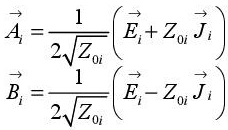
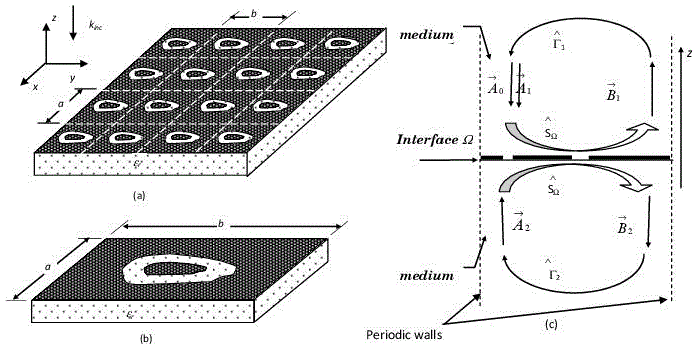
Figure 3.2. a) Geometry of an FSS with dielectric rings taking an arbitrary shape; b) unit cell within the FSS structure; c) section of the unit cell of; b) along the y axis
Zoi is the typical impedance of the medium i. The current density  of the medium i is linked to the magnetic field by the equation:

where  is the normal vector of the interface Ω. The electric field and the current density may be calculated from the transverse waves by the equation:


In referring to Figure 3.2, diffracted waves  are obtained from incident waves
  by applying the diffraction operator
  with the following equation:

The diffracted waves  are reflected across the housing casing covers with periodic walls enclosing the FSS unit cell, and becoming incident waves
  after the addition of the source
  The application of the reflection operator to diffracted waves is given in the equation:

 is the reflection coefficient.
A flow diagram of the WCIP method, applied to FSS, is given in Figure 3.3.
3.2.1. Determining the diffraction operator
The diffraction operator is determined from both the FSS geometry and the interface boundary conditions Ω.
Two types of FSS may be considered. Those FSSs which are uncharged and those which are charged. Charges are inserted within the FSS structure to ensure a better flexibility within the FSS selectivity. Generally, there are three domains: the metallic domain, the dielectric domain and the electrical charge domain. Uncharged FSSs are obtained by associating the charge domain with the dielectric domain or the metallic domain. The charge domain may contain several lumped elements (for example resistances, capacitances, inductances). These three domains are defined by Heaviside's functions, that is to say the equations:


The boundary conditions, at the interface level, within each domain are:

within the metallic domain HM.

within the (dielectric) insulating domain HI.
In the electrical charge domain, the boundary condition is shown by the formula:

The impedance of the surface Zs is calculated from the impedance ZL from the lumped element, using the formula:

where Wz and Lz are the width and length of the equivalent domain of the lumped element.
By applying the boundary conditions to the interface Ω and upon each domain, the global diffraction operator may be calculated by the equations:

with 
3.2.2. Determining the reflection operator
Not knowing the reflection coefficient with the spatial domain, the transition to the modal domain is essential. As a consequence, the projection of diffracted waves on the modal basis must occur before the calculation of the reflected waves. In the case of FSSs, the entire modal basis is made up of the TEM mode, the TEmn modes and the TMmn modes. It is a question of the transition from the spatial domain to the modal domain, which is achieved through using the FMT. When reflected waves are obtained and the source addition is then made, it is necessary to return to the spatial domain via the use of the inverse FMT.
The reflection coefficient within the modal domain is given as the equation:

where  is the admittance of the mnth mode at the medium i and α represents the TE or TM modes. Here
  may be calculated by:
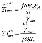
 is the propagation constant of the mode mn within the medium i. It may be obtained by the equation:

εo, εri and µo are, respectively, the permittivity in a vacuum, the permittivity relating to the medium i and the permeability of the vacuum.

Figure 3.3. Flow diagram of the WCIP method
3.2.3. The fast modal transform FMT and its inverse FMT−1
The FMT facilitates the transition from the spatial domain to the modal domain, and the inverse FMT enables the return to the spatial domain with the following relevant equations:
The logical development of [3.15] is set out in [TIT 07a].
3.2.4. FSS multilayer devices
The issue of multilayer FSSs is considered in an inherent way within the analysis of FSSs on a single interface, since the air layer adds to the lower layer and the problem is reduced to being simply the WCIP issue with two media (Figure 3.2) by bringing the admittance of the air layer to the interface for each mode. Generally, multilayer FSSs are dealt with by bringing the admittance of the air layer to the interface Ω, covering the various dielectric layers and using the equation:

Thus, the admittance  is brought back to the interface separating both layers (i+1) and i through the ith layer thickness hi using
  as the ith layer characteristic impedance for the a mode.
3.2.5. Multi-level plated FSSs
Multi-level plating FSSs may be used to achieve multi-frequency band or broadband FSSs. Within the iterative method, the layer separating two consecutive interfaces is modeled as a guide length, and a transition operator between these two layers is defined within the modal domain and is an intermediate stage within the calculation. This operator is given by [GAR 01] with the equation as follows:
with 
hi is the thickness of the layer separating both consecutive interfaces and  is the impedance of the mode mn of the type α, which may be TE or TM.
In Figure 3.4, an example of an FSS double-plated layer and its corresponding diagram are shown.

Figure 3.4. FSS double-layer plating a) section of unitary cell; b) corresponding diagram
3.3. Application of the iterative WCIP method to different FSSs
The iterative method is applied to several types of FSS such as the dielectric short-circuited ring FSSs [TIT 08], the FSS charged with lumped elements and the active FSS [TIT 07], FSS concentric metallic rings [TIT 08], FSS double polarization and FSS broadband. The results obtained with the WCIP method are shown with both the measurement results and/or simulation measurement results to enable a comparison.
3.3.1. Dielectric short-circuited FSS rings
The insertion of two short-circuits and four short-circuits in variable angular positions offers more flexibility in the adjustment of the FSS resonance frequency with circular dielectric rings shown in Figure 3.5. Circular rings are printed on a thickness substrate of 0.51 mm and a dielectric constant of 3.4. The internal radius and the external radius of the dielectric rings are respectively 3.8 mm and 4.5 mm. The dimensions of the unitary cell are a = 11.43 mm and b = 10.13 mm.

Figure 3.5. Circular ring FSS with short circuits, a) FSS with two short circuits; b) FSS with four short circuits
Figure 3.6 shows the reflection coefficient of the FSS in Figure 3.5 when it is fed with a normally incident plane wave in both the x and the y polarizations, respectively. The interface is described as having a grid of 120 × 120 pixels and the iterative procedure is halted after 1,600 iterations.
For increased flexibility within the resonance frequency, two other short-circuits are added in specific angular positions as in Figure 3.5(b). Figure 3.7 shows the reflection coefficient according to the frequency for φ = 20°, 40°, 30° and 60°, when the FSS is illuminated by a normally incident plane wave in the y polarization.

Figure 3.6. Reflection coefficient variation according to the FSS frequency with two short ring circuits with a normally incident source in the x polarization and in the y polarization [TIT 08]

Figure 3.7. Variation of the reflection coefficient according to frequency, with different values for the angular position φ, the four FSS circular ring short circuits with a normal incidence, that is polarized in y [TIT 08], a) φ = 20°, φ = 40° (b) φ = 30°, φ = 60°
The variation of the angular position of the four short-circuits φ = 20° at φ = 100° results in scanning a frequency band which ranges from around 10.9 GHz to 19.2 GHz [MAR 01, TIT 08].
3.3.2. FSSs charged by lumped elements and active FSSs
Using FSSs charged with passive elements and active elements is another alternative way to achieve the FSS concept, with a more variable selectivity. To check that the WCIP iterative method supports charged FSSs, it is applied to a circular FSS dielectric ring, which is charged by capacitors, inductances or PIN diodes.
Figure 3.8 shows the reflection coefficient of this FSS, with a thickness substrate of 0.102 mm and a dielectric constant of 2.4. It has a resonance of nearly 13.9 GHz.
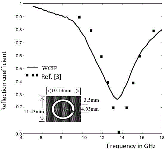
Figure 3.8. Reflection coefficient of an uncharged dielectric FSS circular ring [TIT 08]
3.3.2.1. FSS charged by passive elements
The circular FSS rings are now charged by capacitors and inductances, and corresponding reflection coefficients are shown in Figures 3.9(b) and (c), respectively.
The increase in capacitance decreases the resonance frequency in relation to an uncharged FSS. On the other hand, the increase in inductance also increases the resonance frequency of the FSS, charged with inductances, as Figure 3.9 shows. Hence, a large frequency range, centered upon the resonance frequency of an uncharged FSS, may be detected.
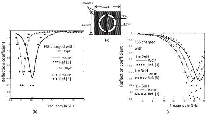
Figure 3.9. Reflection coefficient for FSS devices charged by passive elements [TIT 08], a) the geometry of the charged FSS structure; b) FSS charged by capacitance; c) FSS charged by inductances
3.3.2.2. Active FSSs
To avoid regularly changing the capacitance to vary the FSS frequency, which is charged with capacitors, PIN diodes may be used to give electronically-controlled FSS devices. Active FSS devices are highly significant in compensating for manufacturing errors and adapting the FSS filter to variations in operational frequency of wireless communication systems [TIT 07]. It is enough to vary the reverse bias voltage for the capacitance of the PIN diode to then fluctuate. The inverse polarization diodes may be modeled as a resistance connected in parallel with a capacitance [MAR 05]. As a consequence, the analysis of the active FSS is reduced to the FSS being charged by a charge which has an impedance of the surface Zs (that being obtained from the resistance in parallel with the capacitance modeling the reverse bias diode).
Figure 3.10 shows the reflection coefficient with the same FSS structure. However this time, it is charged with PIN diodes which are polarized with a voltage of −30 V, −3 V and 0 V.

Figure 3.10. FSS unitary cell with circular rings and the FSS with the two rectangular rings: a) FSS reflection coefficient with dielectric circular rings charged with PIN iodes [TIT 08]; b) FSS geometry with two metallic concentric discs [TIT 08]; c) variation of the transmission coefficient according to the operating frequency [TIT 08]
3.3.3. Multi-frequency band FSSs
In the case of FSS single interfaces and for multi-frequency band applications, the metallic concentric FSS rings [TIT 08] or FSSs with fractal geometry [KIM 06] may be used. The open quasi-square FSSs with metallic rings allow two frequency bands in a given polarization direction, and a single frequency band in the perpendicular polarization direction.
3.3.3.1. FSS with metallic rectangular concentric rings
Figure 3.10(a) shows a FSS with two metallic rectangular concentric rings. The structure is fed with a normally incident plane wave. The transmission coefficient represented in Figure 3.10(b) shows the presence of a second frequency band, which is due to the addition of a second ring.
3.3.3.2. Metallic FSS quasi-rectangular open rings
The FSS structure with metallic open quasi-square rings is shown in Figure 3.1(b) and the unitary cell is shown in Figure 3.11(a). The FSS structure is printed on a substrate with both a thickness of 1 mm and a dielectrc constant of 4. Figure 3.11(b) shows the transmission coefficient of the FSS with metallic open quasi-square rings when it is illuminated by a normally incident wave plane in both of the polarizations x and y. This FSS offers scope for precise resonance frequency adjustment for the two frequency bands within the polarization x and that of the single band in polarization y, by varying the coupling length of the parallel FSS strips. The presence of both resonances as well as their variations is due to two strip lengths being understood to have an assumed quasi-symmetrical axis in the y direction. The resonance variation at the time of the polarization of y is caused by capacitance created by both strips, and the increase in the coupling length also increases the facing surface area of the capacitance metallic plates.
3.3.3.3. U-shaped FSS
U-shaped FSSs afford two rejection bands if the source is polarized in the x direction. Figure 3.12(a) shows the metallic pattern U-shaped FSS unitary cell, with dimensions 20 mm x 20 mm. In Figure 3.12(b), the transmission coefficient is shown. The two resonances are controlled by the two lengths d1 and d2, which are both inversely proportional to the resonance frequencies.

Figure 3.11. FSS with an open quasi-square ring [TIT 09]: a) geometry of the unitary cell; b) transmission coefficient
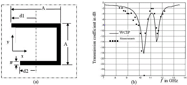
Figure 3.12. Metallic pattern U-shaped FSS with dimensions of: A = 10 mm, d1 = 2.5 mm, d2 = 5 mm, W = 2 mm, εr = 4 and h = 1mm [TIT 09]: a) unitary cell; b) transmission coefficient according to the operating frequency
3.3.4. Double-layer FSS plating
Double-layer FSS plating makes it possible to achieve integrated structures enabling stacked topologies, which are required both within the technology of integrated circuits [WAN 03, BAU 03] and new applications where the target antenna is accounted for with FSS structure in modeling, to take account of mutual interactions [MON 07]. In general, the addition of an interface containing a planar circuit translates as the addition of a resonance. This may also lead to an improvement in the rejected band (or band pass), provided the two resonances are sufficiently near to each other.
3.3.4.1. Rectangular FSS rings across the two interfaces
The double-layer plated FSS structure under consideration is that of Figure 3.4 with εr1 = εr4 = 4.5. This is a substrate of glass fibers labeled “FR-4”. The thickness of both substrates is 1 mm. An air layer with a thickness of 3.3 mm separates both the interfaces Ω1 and Ω2. The external square dimension length of the FSS square ring at the interface Ω1 and that of the interface Ω2 are respectively A1 = 9.8 mm and A2 = 8.2 mm. The width of the metal strip within both of the FSSs is 2 mm. The transmission coefficient of this FSS is shown in Figure 3.13.

Figure 3.13. FSS double-layer plating: a) FSS geometry at levels 1 and 2; b) section of FSS unitary cell; c) power transmitted according to operating frequency
3.3.4.2. Broadband FSS
Multilayer plated FSS devices may afford a broad band of rejection, provided a judicious choice of FSS configuration is made. This type of FSS may serve as a ground plane for transmitter broadband antennas [ERD 02].
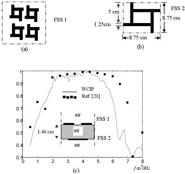
Figure 3.14. Metallic configuration FAN type FSS [ERD 02] with double-layer plating: a) FSS 1; b) FSS 2; c) FSS Reflection coefficient
3.3.5. Triple-layer plating
An increase in FSS bandwidth may be achieved by adding an additional level of plating. In Figure 3.15, identical triple-layer FSS plating is studied through using the WCIP method. The unitary FSS cell etched on the triple-layer plating FSS is shown in Figure 3.15(a). Figure 3.15(b) shows a section of the resulting FSS. Its characterization by the WCIP method is based upon the extension of the FSS double-layer plating approach to that of the triple-layer plating approach, by resorting to inter-level adjacent transition operator specified in [3.17].
Five poles can be noted within the increased bandwidth as Figure 3.15 shows, when characterizing an FSS with identical rectangular slits etched on three levels of plating. Two poles occur due to the resonances of the dielectric thickness, which separates the metal screens. The other poles result from both the resonances of the metal screen and the symmetry displayed by the structure.
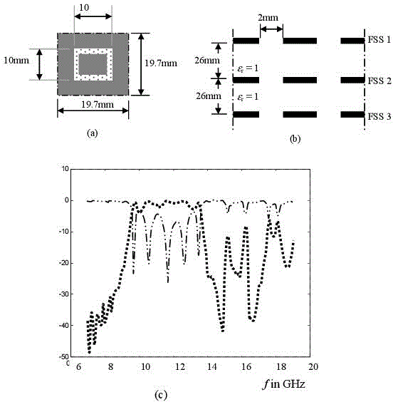
Figure 3.15. Triple-layer plated FSS with identical square slits: a) unitary cell of a square-slit FSS; b) triple-layer plated FSS section; c) reflection coefficient with dielectric rings triple-layer plating FSS obtained by WCIP
3.3.6. Thick FSSs
In reality, the thickness of the metal within FSSs is not always insignificant. As a consequence, significantly thick FSS devices have been studied for several decades [LUE 78]. Improvements in the WCIP method to analyze thick FSSs have been made. Within the thick perforated metallic screens, the screen is considered as a network of identical metallic waveguides. Within the WCIP method this thick screen introduces a level of additional plating and the problem to be resolved is that of double-layer FSS plating. However, in this case both plated layers are enclosed within a non-periodic but metal waveguide.
The thick multi-layer plated FSSs afford structures, which behave as a pseudo-elliptic filter. This is a type of filter which is significant in industry due to its straight band transition characteristics from the pass-band to the stop-band and of the number of transmission zeros that can be adjusted.
3.3.6.1. WCIP method adapted to thick FSS devices
Figure 3.16 shows an FSS with dielectric slits based upon a metal screen placed upon a dielectric substrate, and fed by a plane wave with a normal incidence. The virtual dotted lines in Figure 3.2 represent periodic walls, restricting the FSS unitary cell. A section of the FSS unitary cell FSS under consideration is shown in Figure 3.17. It consists of three so-called regions which are formulated as region I, region II and region III.

Figure 3.16. FSS thick slit resonant FSSs
The dielectric layer made up of air and substrate in Figure 3.17 is converted into a single WCIP layer. This is done by reducing the admittances of the TE and TM modes of the air layer to the interface separating region III from region II passing through the substrate thickness layer h [TIT 7a]. The resulting model shown in Figure 3.18 is the WCIP problem containing three FSS thick slit resonant media.
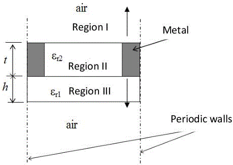
Figure 3.17. Section of the unitary cell of the thick FSS device

Figure 3.18. The three-layer media WCIP issue containing resonant FSS thick slits
Regions I and III are restricted by periodic walls. In these two regions, the conventional WCIP method, adapted to the FSS, is used as explained in detail in [TIT 07a, TIT 07b]. The wave diffracted in region I (or region III) is equal to the part of the wave diffracted from the metallic domain plus the wave coming from region III (or region I) through the rectangular-shaped metallic waveguide. This may be expressed as the equation:

where hm is the indicator function of the metal domain.  are respectively waves coming from region III and arriving in region I, and waves leaving region I to reach region III through region II. Region II is modeled by a rectangular metallic waveguide with a length t being the thickness of the perforated metallic screen.
  are expressed as:
with hi being the indicator function of the dielectric domain filling the metal waveguide, possessing a rectangular shape which models the thickness of the perforated metallic sheet.
 defined within the modal domain is the transition operator crossing both interfaces Ω1 and Ω2, determining the extent of the perforated metal sheet as shown in Figure 3.18. It is expressed by:


where α designates TEmn modes and TMmn, Zα is the impedance of the mode TEmn or the mode TMmn of the metallic surface rectangular waveguide, which is modeled upon region II. Z0II is the characteristic impedance of the dielectric filling the waveguide, limited by the two interfaces Ω1 and Ω2, and γII,mn is the propagation constant of the mode TEmn or the mode TMmn within region II.
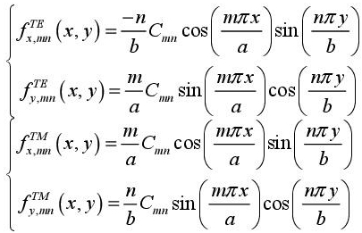
The generating functions of the modes TE and TM of a rectangular metallic waveguide are shown in [WAN 03] described in the following equations:
where the following equations also apply:

Incident waves  across interfaces Ω1 and Ω2 are projected upon the entire modal base [3.21] to determine the amplitudes for modes TE and TM, giving rise to waves that reach regions I and III through metal wave guides replicating the outline of the perforated metal sheet.
To maintain the characteristic of the WCIP method, as regards reduced computational time, through the use of the exponential FFT2 algorithm, a FFT2 algorithm based upon the functions cosi and sico must be derived from the exponential form of an FFT2, being the bi-dimensional Fast Fourier Transform specified in [TIT 07a]. The functions cosi and sico are stated in:
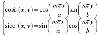
The FFT2 based upon the functions cosi and sico, which characterize the metallic rectangular waveguides, is obtained directly by doubling the structure restricted by periodic walls in the x direction and in the y direction, taking into consideration the wave direction to check the boundary conditions, as shown in Figure 3.19. The region in gray in Figure 3.19 represents the rectangular waveguide restricted by periodic walls.
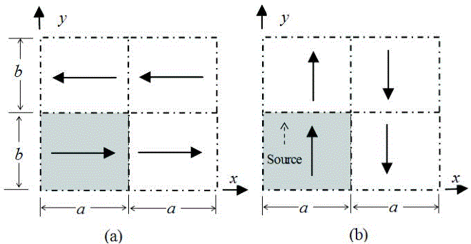
Figure 3.19. Wave direction hi  and i
and i  in the structure when doubled a) according to the x axis direction; b) according to the y axis direction
Incident waves across the structure when doubled in the x axis direction and in the y axis direction are inserted in [3.19] to determine the waves reaching regions I and III, and coming, respectively, from regions III and I via region II.
3.3.6.2. Validation of the improved WCIP method
The FSS structure in Figure 3.16 is analyzed by the method WCIP in which the perforated metal sheet has a thickness of t = 0.0175 cm and slits of dimensions W = 1.32 cm and L = 0.128 cm. The dimensions of the unitary cell are 1.78 cm x 1.78 cm. The FSS structure is fed by a normally incident plane wave and polarized in the y direction. The FSS structure to be analyzed may be used as a radome where a superior dielectric material (the so-called superstrate) may be added to insulate the antenna compartment [MON 07]. The resulting structure was made up of four dielectric layers in which the bottom layer and the top layer are both made up of air. The WCIP multilayer problem [TIT 08] should be applied to bring the TE and TM modes admittance of the air layers to the interfaces Ω1 and Ω2 through the dielectric slabs covering the perforated metal sheet which are the superstrate and the substrate, resorting to the model of the length of the guide. The interfaces Ω1 and Ω2 and the FSS unitary cell are each divided into 128 × 128 pixels and the iterative method is halted after 1,200 iterations.
Figure 3.20 shows the power transmitted and the power reflected according to the thick FSS operating frequency based uniquely upon the perforated metal sheet with a thickness t = 0.175 mm, without either a superstrate or a substrate and without a dielectric medium in the holes. The WCIP approach which is improved and adapted to thick FSS devices is validated in Figure 3.20. In filling the slits by an insulator with a dielectric constant εr = 4, a reduction in the resonance frequency shown in Figure 3.21 was observed comparative to the resonance frequency of the same FSS but without any dielectric in the slits, seen in Figure 3.20.
In Figures 3.22, 3.23 and 3.24 the power transmitted relates to the perforated metallic sheet placed upon a substrate and covered with a superstrate both of the thickness h and of the same dielectric constant εr. The resonance frequency is inversely proportional to the thickness h of the substrate and that of the superstrate.

Figure 3.20. Power both transmitted and reflected according to frequency in the case of a thick FSS with slits filled with air
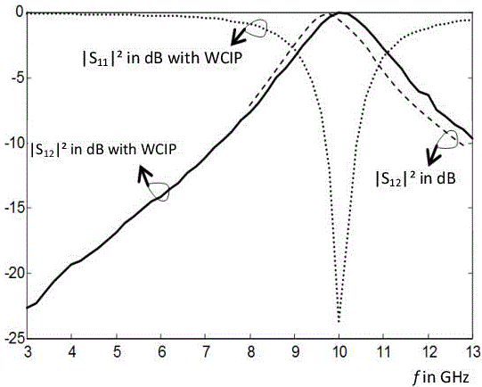
Figure 3.21. Power outputs transmitted and reflected according to frequency in the case of a thick FSS with slits filled with a dielectric medium εr = 4
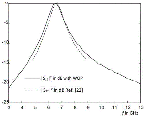
Figure 3.22. Power transmitted through a thick metal sheet with rectangular slots sandwiched between the substrate and a superstrate both being identical and having εr = 4 and h = 0.79 mm

Figure 3.23. Power transmitted through thick metal perforated sheets with rectangular slits sandwiched between a substrate and a superstrate both the same having εr = 4 and h = 1.585 mm
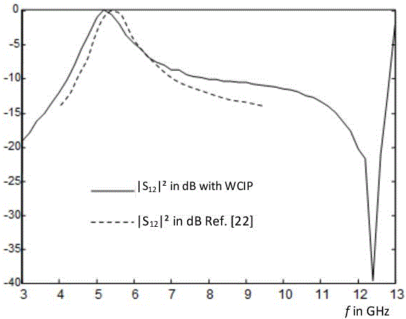
Figure 3.24. Power transmitted through a thick metal perforated sheet with rectangular holes and sandwiched between the substrate and a superstrate both identical with εr = 4 and h = 3.17 mm
The increase in the thickness h results in an increase in the effective dielectric constant of regions I and III with the WCIP triple media issue in Figure 3.18. Consequently, the resonance frequency diminishes as it is inversely proportional to the effective dielectric constant. This property of the material may be applied for an extensive adjustment of the FSS structure. The results of improved WCIP method agree with the simulation results in [MON 07].
To study the effect of the thickness of the perforated metal sheet upon diffraction parameters of the resonant FSS, the power of the non-dielectric FSS, both transmitted and reflected, which is displayed for different values for the sheet thickness t, are shown in Figure 3.25. The power transmitted by the conventional WCIP method and the improved and adapted WCIP method for thick FSSs, for t = 0 coincides to validate the approach of the thick FSS for the WCIP method since the thin FSS which has the value t = 0 is only one particular case of the thick FSS if t = 0. In Figure 3.25 it may also be observed that the resonance frequency of the thick FSS with rectangular holes is directly proportional to the thickness of the perforated metal sheet within the thick FSS, which allows the fine-tuning of the FSS resonant frequency.

Figure 3.25. Powers both transmitted and reflected according to the frequency of a thick FSS in the absence of an insulator in the holes for different thickness values of the perforated metal sheet
Due to the maximal transmission of the power around the resonance for the case of the thick FSS without the dielectric of Figure 3.25, the hole of the unitary cell of the FSS may be represented schematically by a capacitance C in parallel with an inductance L. The capacitance is due to the fringe effects of the rectangular cavity, modeling the metal waveguide of the intermediate region II. Since the majority of modes within the rectangular hole are evanescent, the fields at the interfaces Ω1 and Ω2, which come out of regions I and III, increase when the length of the hole t decreases. Consequently the capacitance C increases and the resonant frequency of the thick FSS reduces.
The power which is both transmitted and reflected in Figure 3.26 relates to the thick FSS structure with rectangular holes, filled with an insulator with a relative dielectric constant εr= 4 for different thickness values for the perforated metal sheet. The perforated metal sheet filled with dielectric material is sandwiched between the air layers. The resonant frequency of the resulting FSS structure diminishes when the thickness of the metal sheet t increases. Hence the possibility of broadening the precision control band of the resonant frequency is present when in the simultaneous presence of both this behavior and that shown in Figure 3.25.

Figure 3.26. Powers which are both transmitted and reflected according to the frequency of a thick FSS with an insulator in the holes with εr = 4 for different thickness values for the perforated metal sheet
In this case the hole consists of a single propagating mode. As a consequence, an increase in capacitance resulting from the presence of dielectric material covering the slits (rectangular-shaped holes) leads to a reduction in the resonant frequency. The same behavior is observed in Figures 3.20 and 3.21, when the insulator is inserted in the holes of the thick FSS sheet.
3.4. Anisotropic FSS
The anisotropic dielectric layers are characterized by less loss comparative to isotropic dielectrics. For the case study relating to the uniaxial anisotropic dielectrics, the approach of the isotropic layer equivalent to the dielectric anisotropic layer is presented in [HOR 80], using a quasi-static approach. A metal strip etched on an anisotropic uniaxial substrate placed upon a metal ground plane is shown in Figure 3.27. The uniaxial dielectric constant of the anisotropic substrate is given in [3.24]:

Figure 3.27. Transmission line on an anisotropic substrate with a system of coordinates
In the case where εxx = εyy the equivalent dielectric layer may have an equivalent thickness heq and a dielectric constant εeq given by [HOR 80], and the following equations apply:
The iterative method is used to characterize an FSS rectangular patch etched on two dielectric anisotropic layers, by adopting the equivalent layer approach presented in [3.25] and [3.26]. In addition, simulation results are given in Figure 3.28.

Figure 3.28. Powers reflected and transmitted according to the operating frequency of a rectangular FSS patch etched on an air-like layer sandwiched between the patch and a dielectric anisotropic layer [TIT 07a, TIT 13]
3.5. Measurement system
The data acquisition system applied for these measurements consists of a microwave network analyzer (of the N5230A Agilent type) which has the ability to increase to a frequency of 18 GHz and possesses two 12 dB amplification cone-shaped antenna, as shown in Figure 3.29. Measurements have been carried out upon FSS sheets of configurations of 10 × 10 unitary cells. The FSSs are made using PCB “Printed Circuit Board” technology with copper. FSS patterns are etched on the substrate of glass fibers known as “FR-4”.
The difference between these measurement results and those of the WCIP is due to the fact that the substrate dielectric constant used is not precisely known; the latter may also be subject to variations when the FSS structure encompasses the various implementation stages through the use of PCB technology.
3.6. Conclusion
The WCIP method is applied to various types of FSS planar structures as follows:
- 1) the FSS with dielectric circular rings charged with passive and active elements for an adjustable selectivity;
- 2) the FSS with two metal rectangular-shaped rings, and the FSS with a U-shaped metal pattern for multiple-band applications;
- 3) the FSS open quasi-square ring for multiple-band applications having two perpendicular polarizations;
- 4) the FSS with double-layer triple-layer plating for multiple-band applications and applications which necessitate large bandwidths and/or very little volume for miniaturization purposes encountered in integrated circuits.
The results obtained with the WCIP method agree both with the measurement results and those of the works in the field.

Figure 3.29. Measurement system and the FSS with metallic rectangular rings
Inhomogeneous layers, which are seen in integrated circuits, are due to the presence of DT “deep-tranch” and/or GR “guard ring” devices used to ensure insulation between the various circuit ports to ensure their anticipated function and to prevent undesired elements coupling. In addition, inhomogeneous layers are present in FSSs in Tera-Hertz applications, when the patterns are made of dielectrics, which are obviously of a given thickness. An integrated model with the WCIP method for thin inhomogeneous layers is being correctly tested.
The WCIP method might be extended to studying multi-layer plating FSS integrated with antennas and antenna arrays, such as arrays of metallic rectangular waveguides, to reduce the volume of the resulting structure if both are independently designed. Furthermore, the interaction between the two is inherently taken into account by the WCIP method. Such structures are necessary to prevent interferences when many communication systems are placed near each other in addition to the possibility of improving the antennas gain.
The WCIP method may also be extended to so-called 3-D (three-dimensional) problems, by using current volume density instead of tangential magnetic fields. This approach will clearly be applied to a dielectric or metal via holes-based problems encountered in substrate integrated waveguide circuits (SIWs).
3.7. Acknowledgments
The authors wish to thank Professor Alfrêdo Gomes Neto of the Telecommunications–Electromagnetism group, the Centre Fédéral de l’Education Technologique de Paraiba, João Pessoa, Brésil (the Telecommunications and Electromagnetism group at Paraiba’s Federal Centre for Technological Education) for all of his measurements used as well as for supplying both the FSS and the measurement system pictures.
Chapter written by Mohammed TITAOUINE and Henri BAUDRAND.


