8Solar Energy: Working at the Edge of Feasibility (1979–2007)
Ovshinsky’s vision of solar energy focused on making efficient and affordable solar panels “by the mile.” While he could clearly imagine this goal, ECD scientists were faced with the enormous practical problems of continuously passing a flexible stainless steel substrate, the web, on which thin layers of amorphous silicon would be deposited, through a series of gas-filled chambers without any cross-contamination. As the physicist Joe Doehler observed, the challenge forced them to work “at the edge of feasibility.”
Over a hundred million dollars was eventually required to prove the concept, but Ovshinsky was equal to the task. His passionate belief in his vision enabled him to persuade the leaders of large corporations to invest the substantial sums needed for ECD’s research, displaying his gift for what Mike Fetcenko called “reeling in whales.” ARCO Solar was the first, investing tens of millions of dollars in Ovshinsky’s solar vision; others included Standard Oil of Ohio, the Japanese electronics giant Canon, and the big Belgian-based wire company Bekaert. All the whales swam away after a few years, usually because changes in management led to their withdrawing support.1 Yet the end of each funding agreement left ECD with greater resources for research and development, and over the next two decades Ovshinsky’s bold plan for mass-producing the solar panels was indeed realized.
ARCO (1979–1983)
Solving the problems of mass-producing amorphous silicon solar panels began soon after Ovshinsky had negotiated ECD’s second, much larger contract with ARCO Solar (see chapter 6). Early in January 1980, he called a series of staff meetings to announce the new effort and to share the ideas he had been developing. Jeff Yang remembered one such meeting on the first day after the holiday break, to which Ovshinsky had brought a pile of books with relevant pages marked. Gesturing with his hands, he began by reminding the group of how a solar cell works and then described his plans to make thin-film cells in large quantities. Yang was impressed when Ovshinsky proclaimed that ECD’s goal would not be to make the best solar cells but rather to change the world by making them cheaply. Only by achieving economies of scale, he argued, could they reach the goal of making fossil fuel obsolete.
But when Ovshinsky went on to present his concept for mass-producing the solar cells by roll-coating them in large volume, those hearing it for the first time were highly skeptical because he had extrapolated from measurements made on tiny fingernail-sized experimental devices to miles of material.2 At another meeting held at Ovshinsky’s home on a Sunday night, Dick Blieden recalled that “virtually everyone there” had serious doubts, and that Steve Hudgens, who had earlier been one of Hellmut Fritzsche’s PhD students and had just joined ECD, muttered something like “this guy is crazy. Maybe I’d better find something else to do.” At the same time, even to the skeptics Ovshinsky’s concept was powerfully attractive. Hudgens remembered appreciating the boldness of “thinking about building a 1-megawatt production plant for thin-film solar when the world market for solar cells was three megawatts.” Ovshinsky’s argument was characteristic of the way he thought about technology: by the time the proposed 1-megawatt machine was built, the market would be 20 megawatts, and when that was achieved the market would be 100 megawatts.3
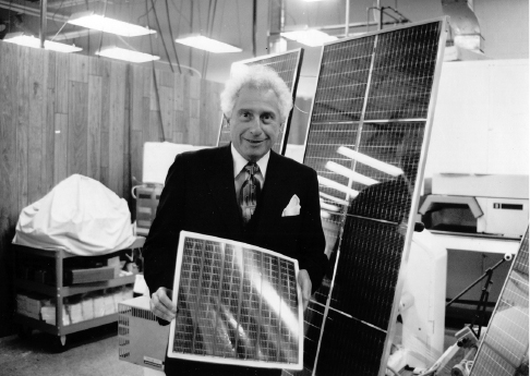
Figure 8.1 Ovshinsky and an Ovonic solar panel, late 1980s.
To appreciate the challenge of building the roll-to-roll machine, we need to review the design of the thin-film solar cells, as discussed in chapter 6, and then consider the manufacturing process. Each cell consisted of three layers of hydrogenated amorphous silicon produced from silane gas (SiH4) by plasma deposition. The P-type layer (doped with a small amount of boron) and the N-type (doped with phosphorus), sandwiched a thicker undoped, or intrinsic (I) layer; these were deposited in sequence on a stainless steel substrate. (Later, two and then three of these PIN cells would be stacked to increase efficiency.) Light shining onto the cell is absorbed mainly in the intrinsic layer and is then reflected back by the substrate. In the electric field created inside the cell by the PIN structure, the electrons freed from the I-layer by the light move to the N-layer, while the holes they leave behind move to the P-layer. When the cell is inserted in a circuit, current flows.
Previously, the layers of N-, I-, and P-type silicon were each deposited separately in a slow and expensive batch process. To deposit them continuously on a moving substrate with plasma-enhanced chemical vapor deposition (PVD) was another story.4 Each layer required a separate gaseous environment, and while the stainless steel web passed through the successive vacuum chambers, the silane gas in each chamber had to be isolated from its neighbors, so that the P and N dopants didn’t get into the I-layer. Preventing such contamination was extremely difficult. Joe Doehler, like Steve Hudgens, first thought, “This is impossible,” and he became even more pessimistic when he went back to his office and did some quick calculations.5 Considering the possibility of using a “gas gate” of differential gas pressure between the chambers to prevent diffusion of impurities from one to the next, he realized that “the degree to which you needed isolation was incredible.” But when he shared his results with Ovshinsky, he recalled, “Stan looked at me and said, ‘Joe, you’re going to prove to me that it doesn’t work or you’re going to make it work.’”6
Doehler then worked on the gas gates with his collaborators in Masat Izu’s group for about a year, making elaborate calculations to understand the fluid dynamics of the gases and adjusting the design of the chambers.7 When they finally succeeded, “it was an intellectual thrill,” he recalled. Keeping the pressure in the intrinsic chamber higher than in its neighbors created a “silane wind” flowing in both directions through the slots that kept out boron or phosphorus atoms. The gas gates were crucial in making the roll-to-roll machine work, though there would be many other problems to solve as ECD built successively larger machines over the years, from the first 1.5-megawatt machine built for Sharp in the early 1980s to a huge 30-megawatt machine by 2005.
Even before the first roll-to-roll machine was completed, Ovshinsky moved quickly to patent it. The job fell largely to the attorney Larry Norris, who joined ECD in the spring of 1980 and worked on patent applications as well as business and license agreements.8 Within a few years more than a dozen basic patents were issued, most with the help of a second patent attorney, Marvin Siskind, who joined Norris in March 1982. Together they built up a patent department at ECD. In the early days, “Larry typically worked on the big picture, and I did much more of the nitty-gritty,” Siskind said. An important objective was to obtain broad enough coverage to control secondary patents dealing with improvements.9
Over the next three decades, Siskind took on the main responsibility for converting Ovshinsky’s confusing explanations into clear patent descriptions. As Mike Fetcenko recalled, “While others would pull their hair out after listening to Stan describing his inventions, Marv was the guy who could turn it into strength.” Siskind realized that Ovshinsky skipped thoughts along the way, often jumbling them, so that what he said was not necessarily what he meant. When Siskind took notes during their meetings he would write what he thought Ovshinsky meant, rather than what he said. “If you couldn’t do that, you would never be able to deal with Stan,” he said.10
In April 1981, when the first of the two ARCO grants covering solar work ended, Ovshinsky attempted to extend and increase the R&D and cross-licensing agreement to a full-fledged joint venture.11 But, unlike Bradshaw, the new executive vice president of ARCO Solar didn’t share Ovshinsky’s vision, and ARCO “really didn’t think big company–little company joint ventures work,” Nancy Bacon explained. Soon Ovshinsky was talking with both Sohio and Sharp in his efforts to raise further support. Making the new agreements was aided considerably by the fact that when the ARCO agreement ended, ECD was able to keep the technologies that had been developed, a coup that John de Neufville attributed to “the fine negotiating skills of Nancy Bacon.”12 These favorable terms set a precedent for ECD’s negotiations with later patrons. With each successive partner in the solar program, as well as with most of those in the other energy and information programs, ECD was able to keep both the intellectual and physical property that had been created under the collaboration. As we shall see, these cumulative gains eventually enabled the company to grow from a contract R&D lab into an independent manufacturer.
Sohio and Sharp (Early to Mid-1980s)
Ovshinsky negotiated agreements in 1981 with the Cleveland-based Standard Oil of Ohio (Sohio) and at the same time with Sharp of Osaka; the result was overlapping joint ventures.13 ECD’s initial contact with Sohio concerning photovoltaics occurred late in 1980, when Ovshinsky’s old Akron friend Harvey Leff put Bacon in touch with Sohio’s Dick Smith, who in turn negotiated with Ovshinsky. Sohio was at this point rich from its oil fields on the north slope of Alaska, and like other oil companies was hedging its bets by building a broad portfolio that included a number of alternative energy approaches. To help him with the negotiations, Ovshinsky brought in Dick Blieden, who had been instrumental earlier in arranging the ARCO Solar contract (see chapter 6). Blieden worked initially on a consulting basis and eventually joined ECD’s staff.
In negotiating with Sohio, Ovshinsky said he wanted to build a 4-megawatt machine, but Sohio negotiated it down to a demonstration 2-megawatt pilot production machine, the TA2 (Tandem Two) machine, designed to create double (i.e., six-layer) cells, for reasons of efficiency discussed later in this chapter. ECD’s contract with Sohio ultimately contributed some $80 million of funding for solar, as Bacon recalled, supporting considerable research aimed at improving the efficiency of the solar cells.
Before the negotiation with Sohio was concluded, ECD also agreed to build a 1.5-megawatt machine for Sharp, the TA1, which created single three-layer cells.14 At the time Sharp joined with ECD, it had one of the biggest solar cell manufacturing operations in Japan, but their cells were made of crystalline silicon. When Tadashi Sasaki of Sharp learned about the pilot production machine that ECD was building, he wondered whether using a roll-to-roll machine to produce amorphous solar cells could also fit Sharp’s needs. He negotiated the deal that resulted in the Sharp machine, built between the summers of 1982 and 1983 during the early years of ECD’s joint venture with Sohio. ECD then disassembled and delivered the machine to Japan in August 1983, where it was used by Sharp for some years.
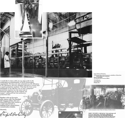
The TA1, ECD’s first commercial roll-to-roll machine, produced small solar cells for use in hand-held calculators, the first products that used amorphous silicon. Ovshinsky would proudly hand out the $10 solar-powered calculators to employees and visitors. To commemorate the historic achievement, he had a poster made that juxtaposed a picture of the Sharp machine with one of Ford’s Model T, the first affordable, mass-produced automobile. Just as Ford’s assembly line replaced the slower, more expensive process of making cars one by one, ECD’s roll-to-roll machine replaced the slower, more expensive batch production of solar cells. As we discuss in chapter 11, this experience with amorphous silicon solar panels later enabled Sharp to make thin-film transistors (TFTs), eventually used in their work on flat panel displays.
Figure 8.2 Poster comparing Ovshinsky’s roll-to-roll machine to Ford’s Model T assembly line.
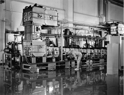
Figure 8.3a The Sharp machine in Japan.
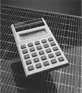
Figure 8.3b Sharp solar-powered calculator.
The efforts to increase the efficiency of the amorphous silicon solar cells proceeded simultaneously along multiple tracks. While contamination had been the largest problem in designing the roll-to-roll machine, now the largest problem was the Staebler-Wronski effect. This had been discovered at RCA in 1977 by David Staebler and Christopher Wronski, who found that exposing amorphous silicon solar cells to sunlight over a six-month period causes a 10–30% decrease in efficiency.15 While this degradation can never be completely eliminated, ECD developed various strategies to minimize it. The most important was making the intrinsic layer so thin that nearly all the electron-hole pairs created when light impinges on the cell can be collected by the electrodes before they recombine and create defects. Thinner solar cells, however, absorb proportionately less light than thicker ones, so the team stacked first two and later three thin cells on top of each other. A reflective layer at the back sent the remaining light up through the cell to generate more current.
Stacking two or three thin solar cells (i.e., increasing from three to six or nine layers) also opened the way to “spectrum splitting,” developed in the early 1980s by Steve Hudgens, in which the stacked cells are not compositionally or optically identical. Incorporating different proportions of germanium in the silicon allowed the layers to absorb different light wavelengths.16 The concept did not originate with ECD, but the material produced elsewhere was poor. ECD perfected the process. “Nobody else knew how to make silicon germanium alloy better than ECD,” Jeff Yang said. In the triple cell, the top cell captured the blue end of the spectrum; the bottom cell captured the red, and the middle cell all the frequencies in the range in-between. The result was that over the course of the day, the newly designed solar panel used more of the solar spectrum than do ordinary crystalline cells; it “wakes up earlier, goes to bed later, and performs better in high heat and diffused light,” explained Steve Heckeroth, an architect and builder who installed the solar panels in several of his projects.
Other important contributions to improving efficiency came from Subhendu Guha, who arrived at ECD in February 1982. The respected physicist had been working on amorphous hydrogenated silicon for about five years.17 Finding a paper by Ovshinsky on using fluorinated amorphous silicon “of interest,” Guha wrote to him asking whether he might come to ECD for his upcoming academic sabbatical leave from the Tata Institute of Fundamental Research in Bombay (now Mumbai).18 Ovshinsky replied that he had heard about Guha’s work and suggested he come to ECD for two years. Guha joined the group then headed by Hudgens.19 After some months, Guha accepted Ovshinsky’s invitation to stay on indefinitely, and within two years he had risen to be manager of the Advanced Research Group.
Soon Guha and Yang were collaborating on further increasing the efficiency of the solar cells, in which they made two major advances. The first was finding a way to invert the cell structure, from PIN, where P is on the bottom, to NIP, where P is on top. Basic physics principles indicated that it would be better to have the light enter through the P-layer, but the amorphous P-type material is very absorbent and so lowers the efficiency of the whole device. Guha suggested making the P-layer of microcrystalline rather than amorphous silicon, which made the NIP structure possible because microcrystalline silicon has higher conductivity and is less absorbent.20 The second advance, known as “band gap profiling,” increased the efficiency by varying the germanium/silicon ratio continuously over the thickness of each intrinsic layer.21 Both advances substantially increased the efficiency, raising it to a record-setting 13%.
When Yang announced ECD’s new efficiency record at a conference, however, he found himself in a bind because of Ovshinsky’s commandment, “Thou shall not disclose the device structure.” So when, in response to Yang’s talk, someone asked him, “What is your device structure? Is it NIP or PIN?” he replied, “It depends on which way you look at it.”
Sohio’s generous support had led to remarkable progress in the design of the cells, but after five years British Petroleum, which had taken over Sohio, ended the agreement. “BP just wanted to focus on oil,” Blieden said. But once again, with the help of Bacon and the attorneys, ECD benefitted from the dissolution. When Sohio-BP withdrew, they “left ECD with more technology, more understanding and in complete ownership, which allowed us to go forward and make a new deal,” said Herb Ovshinsky, who added that “every back-out turned out to be for the benefit of ECD. Every single one.” “It was sort of like swallowing an elephant,” Blieden added, “because we had this small company.”
But after ECD had swallowed the elephant there was little more to eat for some years. Ben Chao remembered “big layoffs in 1986 and 1987. We lost at least 40% of our people; maybe three hundred people left.”22 Those who remained at ECD during those dark days were sustained by their belief in Ovshinsky’s goal “to make the planet a better place to live,” Chao said. And once ECD’s financial situation improved, “a lot of people came back.”
In the midst of the lean years, a new funding opportunity arose from one of ECD’s many patent disputes. Canon, a major manufacturer of copiers, was trying to make its copier drums with amorphous silicon instead of such toxic materials as selenium and arsenic. Because they were using the technique of plasma-enhanced chemical vapor deposition developed by ECD, the patent attorneys Marv Siskind and Larry Norris went to Japan, as Siskind said, “basically to charge Canon with patent infringement. They were doing it with radio frequency, but nonetheless they were doing it.” The discussion eventually took a more positive turn. “After a while,” Siskind recalled, “we convinced them we’re not just here to say hey, you have a patent problem, but we think we can help you out with your commercialization. And so things changed quite a bit.” As a result, Canon agreed in 1985 to pay ECD $10 million to develop the drums. Steve Hudgens solved the problem of depositing the required 30 microns of amorphous silicon at a high rate by changing to microwave frequency. Developing the license agreements for Canon’s copier technology began what would become a close business relationship, leading eventually to a 1990 joint venture in solar energy. Meanwhile, as Siskind said, ECD “lived off of Canon in the last part of the 1980s.”
Canon: Creating United Solar Systems (1990–2000)
After ECD’s work on the copier drums, Canon expressed interest in buying a research machine for making solar cells.23 This initiative became the occasion of another financial drama, which began on a Monday morning when Ovshinsky told Jeff Yang that ECD might not be able to meet the payroll at the end of the week unless they could demonstrate the machine’s capacity to make a 12% silicon cell while a visiting Canon scientist watched. “It was kind of like having a gun at your head,” Yang said. At this point the band-gap-profiling concept was not yet fully developed, so making a triple junction cell with the required efficiency in a few days was “like running before you were walking.” But on Thursday they crossed the 12% threshold, and Canon agreed to pay a million dollars to have the machine dismantled and rebuilt in Japan. Then another plot twist came when it turned out that the money couldn’t be moved from Japan by the next day. Nancy Bacon suggested selling the machine to Canon USA instead; the lawyers and accountants worked through the night, and by Friday the money for the payroll was in the bank.
The pressure continued even after ECD convinced Canon to begin supporting solar work while they were still arranging the joint venture. Yang recalled the grueling negotiating sessions: arriving in Tokyo in the evening, starting early the next morning and continuing for twelve hours, then dinner followed by an invitation to karaoke. “Subhendu was polite enough to say yes, but I said I really can’t. Then at 7 o’clock the next morning, it starts all over, with the minutes of yesterday’s whole discussion on a white board, day after day after day!”
The work with Canon in the pre-joint venture period was uncomfortable for other reasons, too. Guha recalled that he and Yang were sent to Japan to meet Hiroshi Tanaka, Canon’s aggressive and imaginative senior managing director, known as “Tiger Tanaka.” Before the meeting Yang and Guha met Momoko Ito for breakfast. She greeted them with “Congratulations on getting 15% efficiency.” “I beg your pardon?” Guha responded. “You didn’t get 15%?” she asked. He explained that they were then at roughly 13%. “Oh my god,” she replied and promptly went to work to straighten matters out. Besides the embarrassments caused by Ovshinsky’s tendency to exaggerate, he was also sometimes challenging for Canon’s representatives to negotiate with. When Tanaka complained that Ovshinsky had misled him, Ovshinsky fired back with “What do you know about science?” Ovshinsky’s tough negotiating style and characteristic demands for “more” could create tensions with his partners and sometimes contributed to the breakdown of collaborations. That did not happen in this case, but it does seem to have contributed to a shift in his role in ECD’s solar program.
When the agreement with Canon was finally concluded in 1990, it was for a 50/50 joint manufacturing venture separate from ECD, to be called United Solar Systems (USSC).24 Since the funding was coming entirely from Canon, they controlled the new company, including, crucially, its operational management. Ovshinsky had thought Guha would continue doing research in ECD while United Solar handled production, but Canon preferred to bring Guha into the joint venture. He thus became responsible for the operations of the new organization, becoming vice president for research and technology and later executive vice president in charge of both research and production. Canon was represented by a series of executives who typically came for a week each month.
The birth of United Solar was an important turning point in ECD’s history. On the one hand, it greatly advanced Ovshinsky’s vision of mass-producing thin-film solar panels, of which the new company eventually became the largest manufacturer. But in the process, he gradually lost control of the solar effort.25 Under Canon, ECD’s solar program was transformed from an R&D into a manufacturing operation. “We learned a lot from Canon,” Guha remarked. “We learned manufacturing. They taught us you run it as a real company, not as an R&D company anymore. To be truthful, at the time ECD did not have a clue as to how to do manufacturing. Manufacturing is a different discipline. You don’t make big changes. Canon’s philosophy is what is known in Japan as kaizen. Make small changes—don’t make big changes.” That disciplined conservative approach was the antithesis of Ovshinsky’s bold decision to go directly from solar cells measured in centimeters to making continuous panels by the mile. He could imagine and inspire that dramatic effort, but he was not so well suited to directing its day-to-day operations.26
By 1997, United Solar had a 5-megawatt plant in Troy producing triple junction panels in 12-inch- and later 14-inch-wide rolls. The coated webs were cut into panels in Mexico in a maquiladora operation just south of San Diego, where the labor-intensive finishing processes of laminating and adding connections could be done at lower cost. But outsourcing the last stage of production caused problems when it came to installing the panels. Some got bent during shipping from Mexico and had to be expensively rewired by electricians after installation, and the adhesive initially used for attaching the panels melted at 180 degrees and even, as the talented Indian-born engineer and technician Arun Kumar recalled, “caught fire big time.” Steve Heckeroth encountered many of those problems in using United Solar roofing on projects in northern California. He tried to raise these issues after Ovshinsky appointed him ECD vice president of building-integrated photovoltaics, but that just created conflict with United Solar management, who resisted Ovshinsky’s interference. Heckeroth found this all “hard to watch” because he felt ECD’s solar product was outstanding and “they could have been so far ahead of everybody.”
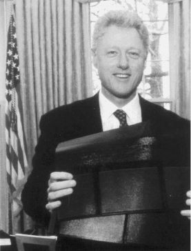
Figure 8.4 President Clinton in the Oval Office, holding an Ovonic solar panel.
Such problems were in time corrected, and United Solar became very successful, even winning an endorsement from the White House. “You remember those solar panels, how big they used to be?” President Bill Clinton said, holding up a United Solar panel. “Look at this. I want everybody to look at this and consider this for your home. Look how thin they are. It’s really an amazing thing, and most Americans have not yet seen these, but they can make a huge difference in what we have to do.”27
Ovshinsky’s role in all this, however, was reduced, and his attention shifted to other research areas such as hydrogen and fuel cells (see chapter 9). Eventually, as with the ARCO and Sohio joint ventures, the partnership with Canon ended with a change in its management. Tanaka, the greatest proponent of photovoltaics, lost his battle for power in the company, and the new president, as Robert (Bob) Stempel later put it, “took the view that nothing should be Canon’s business unless it had a lens.”28
Sovlux (1990–1996)
In 1990, while the Canon joint venture was underway, ECD also formed Sovlux, a joint venture with Kvant, which was a part of the Soviet nuclear industry. ECD built a huge 2-megawatt photovoltaic machine in Michigan, then disassembled and shipped it to Moscow to be reassembled and installed. By the time it arrived, however, the Soviet Union had dissolved, and both installing it and getting payment from the Russians took longer than expected. A large ECD team, headed by Roger Woz, spent a long time working in Moscow to get the Sovlux machine running. Arun Kumar was the main troubleshooter, the one who “made sure the machines ran properly and the electric work was done well,” Ovshinsky said. “If there was a noise, he’d stay up all night to find out where the noise came from.” Kumar spent so much time there that he learned to speak Russian. He found that the machine had sat on the docks for months, and most of the electronics had become corroded by the salt air. “So the moment we got there, we took a lot of time cleaning that stuff out and getting it to work.” By 1996, the ECD team had the machine running and turned it over to the Russians.
Bekaert (2000–2005)
Around the time when Canon was preparing to pull out of the United Solar joint venture, Guha received an inquiry from Bekaert, a large Belgian-based manufacturer.29 He first thought they wanted to sell something to ECD, but when their representative arrived and expressed interest in investing, “that certainly got my attention,” he said. Bekaert wanted to get into alternative energy, and after looking at all the current solar programs had chosen United Solar as the most promising. They initially proposed a tripartite venture, but Canon preferred to leave, so Bekaert bought out Canon’s share, and in June 2000 ECD and Bekaert formed a 50/50 joint venture. As with the Canon venture, all the money—over $80 million—came from Bekaert, so they were in control, but they left the R&D and manufacturing with United Solar while putting in their own sales and marketing staff. Also like Canon, Bekaert stipulated that Guha remain in charge, and he now became president of United Solar.
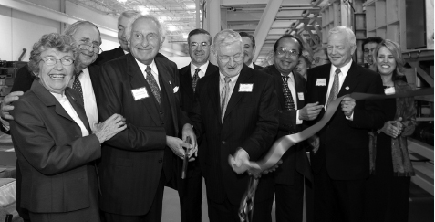
The new investment led to another giant step in production capacity. From the 5-megawatt capacity of the Canon machine, Bekaert agreed to the ambitious goal of building a 25-megawatt machine.30 The key to this advance was Herb Ovshinsky’s suggestion to turn the stainless steel web on its edge, running six rolls vertically at once.31 Like Ovshinsky’s original roll-to-roll concept, it was an extremely complex engineering task, requiring a high degree of teamwork, but again the ECD staff succeeded. The ribbon-cutting ceremony in July 2005 for the plant in Auburn Hills, Michigan, was attended by US secretary of energy Samuel Bodman, who gave the keynote speech. Over the next few years, the first plant was joined by a second, and then two more were built in Greenville, each with four production lines, which gave ECD’s solar program an enormously increased capacity.
Figure 8.5 The ribbon-cutting ceremony for the 25-megawatt plant, July 2005.
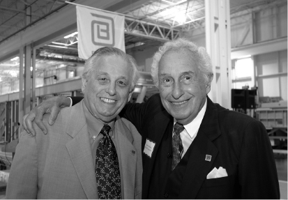
Figure 8.6 Herb and Stan Ovshinsky at the ribbon-cutting ceremony.
Partnering with Bekaert also helped ECD find new markets for solar panels, especially in Europe, where there was increased interest in solar power after the Chernobyl nuclear accident and generous subsidies in Germany. United Solar’s thin-film laminated roofing panels gained increasing acceptance, and by 2009, 80 percent of their greatly enlarged production was being exported.32 By then, however, the partnership with Bekaert had ended. Once again, a change in leadership led to the breakup. With the declining European economy, Bekaert’s new management became increasingly worried about the high cost of the new machine and whether it would really work. Eventually Bekaert decided not to continue, and in 2005 ECD bought them out for a fraction of what they had invested. “In retrospect,” Bob Stempel noted, “that’s one of the great things that happened for United Solar, because now the machine was ours.” Several months later the machine began running, producing good material. “The sad part,” Stempel added, “was the people from Belgium who helped us bring the machine up to speed. When they found out their company was going to leave, those guys were actually in tears some of them, because they knew the machine was ready to run and produce.”
Once again, ECD had benefited from the ending of a major joint venture. United Solar became a fully owned subsidiary and the largest US manufacturer of thin-film solar panels. It was now primarily oriented toward increasing production, though it also continued research on improving efficiency.33 Guha stressed how much the company had gained from its large corporate partners. “We learned a lot from Canon in terms of manufacturing. We learned a lot from Bekaert in terms of financial discipline.” But, he also emphasized, “the innovation came from ECD.”
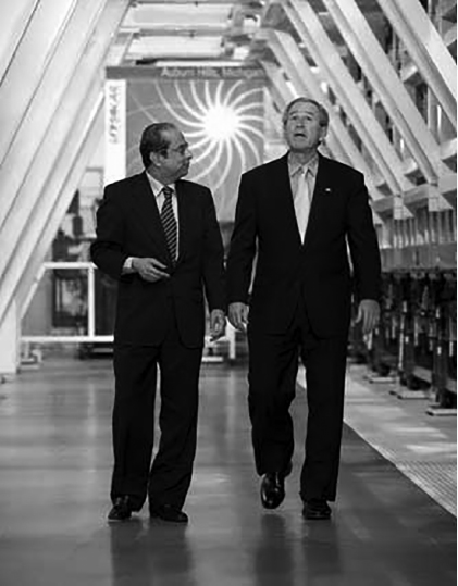
It appeared by 2005 that a tipping point had been reached in the world’s appreciation of the need for alternative energy. United Solar’s large area solar panels were selling so well that they had a backlog of orders. Even President George W. Bush, who as Ovshinsky said had been “brought up as an oil person,” took notice of ECD and its impressive solar energy efforts when he visited the United Solar plant in Auburn Hills on February 20, 2006.34 Despite having very different politics from Bush, Ovshinsky welcomed the visit: “First of all, he’s President of the United States, and he came to see something that he normally would not.”
Figure 8.7 Subhendu Guha showing President Bush the new solar plant, February 2006.
For several years after ECD bought out Bekaert, United Solar dominated the amorphous silicon solar panel market. Over the course of twenty-five years, ECD had developed an outstanding product, cheaper than crystalline solar cells, adaptable to more kinds of installation, and much less fragile.35 Ovshinsky, however, wanted more. Still intent on making solar energy cheaper than fossil fuel, he proposed another huge jump in production capacity, from the 25- to a 1,000-megawatt (1-gigawatt) machine. The concept depended on depositing the amorphous silicon at a much higher speed and would require an enormous investment of new funds. Guha and others at United Solar didn’t think this was a feasible or affordable goal, or that it was needed. In time, Ovshinsky would proceed with the gigawatt concept on his own (see chapter 12).