6
Controlling Light Propagation with Interfacial Phase Discontinuities
This chapter is devoted to the phase response of plasmonic antennas and their applications. Plasmonic antennas are optical resonators that convert light propagating in free space into spatially localized energy. These antennas have a wide range of potential applications [1–6]. One of the main themes of previous research efforts has been the capability of optical antennas in efficiently capturing and concentrating light power; however, the antenna phase response and its implications in controlling the propagation of light have not been systematically studied and will be the focus of this chapter. This chapter is organized as follows.
Part I of the chapter discusses a few models with varying complexity that illustrate the physics behind the phase response of optical antennas. In Section 6.1, we provide an intuitive physical picture in analogy to the impedance of electric circuit elements, where the evolution of charge, current, and near-field distributions of an optical antenna across a resonance is explained. Sections 6.2 and 6.3 discuss 1D and 2D oscillator models considering explicitly the radiation damping effects besides the ohmic absorption losses for plasmonic antennas supporting one plasmonic mode and two independent, orthogonal plasmonic modes, respectively. Section 6.4 presents the results of two analytical models based on solving rigorous integral equations of antenna currents that consider retardation effects and near-field interactions. We adapt methods used in radio frequency antennas for optical frequencies and verify the validity of our models by comparing the results with full-wave simulations. Section 6.5 discusses the properties of V-shaped optical antennas by mapping out their two plasmonic eigenmodes and polarization conversion properties. These antennas are ideal examples of 2D plasmonic structures and are the building blocks of antenna arrays to be discussed later in the chapter.
Part II of the chapter discusses several applications of phased optical antenna arrays, dubbed “meta-interfaces, ” which are able to mold the incident wavefronts into desired shapes over a propagation distance comparable to the optical wavelength. These include demonstration of generalized laws of reflection and refraction in the presence of linear interfacial phase distributions, demonstration of giant and tuneable birefringence, and generation of optical vortices that carry orbital angular momentum.
6.1 PHASE RESPONSE OF OPTICAL ANTENNAS
6.1.1 Introduction
In the field of physical optics, which explores the propagation of electromagnetic waves, the general function of most optical devices can be described as the modification of the wavefront of light by altering its phase and amplitude in a desired manner. The class of optical components with a spatially varying phase response includes lenses, prisms, spiral phase plates [7], axicons [8], phase retarders, and more generally spatial light modulators (SLMs), which are able to imitate many of these components by means of a dynamically tuneable spatial phase response [9]. Another class of optical components such as gratings and holograms is based on diffractive optics [10], where diffracted waves from different parts of the components interfere in the far field to produce the desired optical pattern. All of these optical components shape optical wavefronts by relying on gradual phase shifts accumulated during different optical lengths. This approach is generalized in transformation optics [11, 12] which utilizes metamaterials to engineer the spatial distribution of refractive indices and therefore bend light in unusual ways, achieving such phenomena as negative refraction, subwavelength-focusing, and optical cloaking [13, 14].
It is possible to break away from our reliance on the propagation effect and attain new degrees of freedom in optical design by introducing abrupt phase changes into the optical path [15–20]. This can be achieved by using the large and controllable phase shift between the excitation and radiated light of optical resonators. This approach enables the design of a new class of optical devices with pixelated phase elements, which are thin compared to the wavelength of light. The choice of optical resonators is potentially wide-ranging, from nanocavities [21, 22], to nanoparticles clusters [23, 24] and optical antennas [1, 2]. We concentrated on the latter in this chapter, due to their widely tailorable optical properties and the ease of fabricating planar antennas of nanoscale thickness. In general, resonant behavior can be found for any type of vibration, including mechanical, electrical, optical, and acoustic, among others, and can be utilized in the manipulation of these various kinds of waves (e.g., [25, 26]).
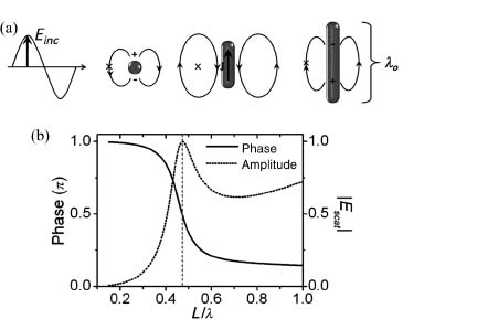
The phase shift between the scattered and incident light of an optical resonator sweeps a range of ∼π across a resonance. This π phase shift across resonance is observed in many other resonator systems between the response of a resonator and its driving force (e.g., when the frequency of an applied force tunes over the resonant frequency of a mechanical harmonic oscillator). Without resorting to any rigorous theoretical models or full-wave simulations, let us first gain a physical understanding of this phenomenon qualitatively by analyzing the phase response of a straight optical antenna of length L. If the antenna is optically small (L/λo << 1), its charge distribution instantaneously follows the incident field (Fig. 6.1a, panel two), that is,  where
where  is the charge density at one end of the antenna. Therefore, the emitted electric field, which is proportional to the acceleration of the charges (Larmor formula [27]), is
  That is, the incident and scattered fields are π out of phase. At antenna resonance (L/λo ∼ 1/2), the incident field is in phase with the current at the center of the antenna (Fig. 6.1a, panel three), that is,
  and therefore drives the current most efficiently. As a result,
  the phase difference between
  and
and  is π/2. For a long antenna with length comparable to the wavelength (L/λo ∼ 1), the antenna impedance (defined as the incident field divided by the current at the center of the antenna) is primarily inductive, or
  Consequently, the scattered and incident light are almost in phase (Fig. 6.1a, panel four),
  In summary, for a fixed excitation wavelength, the impedance of an antenna changes from capacitive, to resistive, and to inductive across a resonance as the antenna length increases. A single antenna resonance therefore is only able to provide a range of phase change at most π between the scattered and incident light.
FIGURE 6.1 (a) Schematics showing the instantaneous distributions of charge, current, and near field (represented by electric field lines) of rod antennas of different sizes when the incident electric field (first panel) is upward and has the largest amplitude. A perfectly conducting metal is assumed and antennas are in the free space. The second panel shows that maximum amount of charges accumulates at the ends of an optically small antenna with length L << λo and the current on the antenna is zero. The third panel shows that the instantaneous current on a resonant antenna with L ≈ λo/2 is maximum and is in phase with the incident field, while there are no charge accumulations. In the last panel, for an antenna with L ≈ λo, again the charge accumulation is maximum (but located at a distance of about L/4 from the ends [28]) and there is no antenna current. Let us take a monitor point λo/4 away from the antennas (the crosses in the second, third and fourth panels of Fig. 6.1a) and count the phase difference ΔΦ between the antenna radiation at that point and the incident field. One can easily tell that ΔΦ is π, π/2, and 0 for the three antennas with L << λo, L ≈ λo/2, and L ≈ λo, respectively, by comparing the electric field lines around the antennas and the instantaneous incident field. (b) Amplitude and phase response of a rod antenna as a function of antenna length calculated by analytically solving Hallén's integral equations for linear antennas [28]. The antenna is located in vacuum and has a circular cross-section with radius r = L/50. Incident monochromatic light impinges normal to the rod and is polarized along it. The scattered light is monitored in the far field along the direction of the incident light.
6.1.2 Single Oscillator Model for Linear Optical Antennas
In this section, we describe a simple oscillator model for optical antennas and, in general, any nanostructures supporting localized surface plasmon resonances (LSPRs) [29, 30]. The model treats the resonant, collective oscillations of electrons in the nanostructure as a damped, driven harmonic oscillator consisting of a charge on a spring. Unlike previously proposed models in which all damping mechanisms were combined into a single loss term proportional to the charge velocity [31–33], we explicitly account for two decaying channels for LSPR modes: free carrier absorption (internal damping) and emission of light into free space (radiation damping) [16].
We begin by analyzing a system in which a charge q located at x(t) with mass m on a spring with spring constant κ (Fig. 6.2a) is driven by an incident electric field with frequency ω and experiences internal damping with damping coefficient Γa:
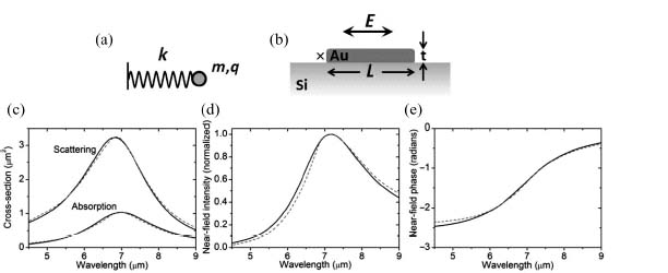
FIGURE 6.2 (a) Representation of an optical antenna in oscillator form, where q is the charge, m is the inertial mass, and x(t) is the displacement from the equilibrium position. (b) Schematics for FDTD simulations. A gold optical antenna (length L = 1 μm, thickness t = 50 nm, width w = 130 nm) sits on a silicon substrate and is illuminated by a normally incident plane wave polarized along the antenna axis. The cross represents the point ∼4 nm away from the antenna edge where the near field is calculated. Complex permittivity of gold is taken from Palik [42]. (c) Scattering and absorption cross-sections as calculated via FDTD (dashed curves) and the model (solid curves). (d) Near-field intensity calculated by the oscillator model (solid curve) and via FDTD (dashed curve) at the location identified by the cross, with the incident field subtracted off. (e) Oscillator phase (solid curve) and the phase of the near field calculated via FDTD (dashed curve).
In addition to the internal damping force Fa(ω) = Γadx/dt, the charge experiences an additional force Fs(ω) = Γsd3x/dt3 due to radiation reaction, where  This term describes the recoil that the accelerating charge feels when it emits radiation that carries away momentum and is referred to as the Abraham–Lorentz force or the radiation reaction force [34]. The recoil can also be seen as the force that the field produced by the charge exerts on the charge itself [35]. For our charge-on-a-spring model, the radiation reaction term has to be included for physical consistency and cannot be absorbed into the internal damping coefficient Γa.
By assuming harmonic motion x(ω, t) = x(ω)eiωt we can immediately write down the steady-state solution to Equation 6.1 as
where x(ω) contains the amplitude and phase response of the oscillator and  The time-averaged absorbed power by the oscillator can be written as Pabs(ω) = Fa(ω)*(iωx(ω)), where Fa(ω)* is the complex conjugate of the internal damping force. Similarly, the time-averaged scattered power by the oscillator is Pscatt(ω) = Fs(ω)*(iωx(ω)). Therefore, we have
where
Our oscillator model can shed light on the relationship between the near-field, absorption, and scattering spectra in optical antennas. If we interpret the optical antenna as an oscillator that obeys Equations 6.1, 6.2, 6.3, 6.4, and 6.5, we can associate Pscat and Pabs in Equations 6.3 and 6.4 with the scattering and absorption spectra of the antenna. Furthermore, we can calculate the near-field intensity enhancement at the tip of the antenna as |Enear(ω)|2  |x(ω)|2 [30].
By examining Equations 6.3 and 6.4 and noting that Pscat  ω2 Pabs
  ω4|Enear(ω)|2 we can deduce that the scattering spectrum Pscat(ω) will be blue-shifted relative to the absorption spectrum Pabs(ω), which will in turn be blue-shifted relative to the near-field intensity enhancement spectrum |Enear(ω)|2. This is in agreement with experimental observations that the wavelength dependence of near-field quantities such as the electric field enhancement can be significantly red-shifted compared with far-field quantities such as scattering spectra [36–41]. These spectral differences can also be clearly seen in finite difference time domain (FDTD) simulations of gold linear antennas on a silicon substrate designed to resonate in the mid-infrared spectral range (Fig. 6.2b). In Figures 6.2c–6.2e, we show the scattering and absorption cross-sections, the near-field intensity, and the near-field phase, respectively, for our antenna as calculated by FDTD (dashed lines). We fit the simulation results presented in Figure 6.2c with Equations 6.3 and 6.4 to obtain the parameters q, m, ω0, and Γa. The resulting model is able to explain the peak spectral position and general shape of the near-field intensity (Fig. 6.2d), as well as the phase response of the antenna (Fig. 6.2e). Note that no additional fitting was done to obtain the near-field curves in Figures 6.2d and 6.2e. This result suggests that this model can predict the near-field amplitude and phase response from experimental far-field spectra of antennas, which are much easier to obtain than near-field measurements.
The parameters obtained from the fit are consistent with the interpretation that the driving and radiative damping of the antenna mode are due to conduction electrons in the antenna. Assuming a carrier density of 5.9 × 1022 cm−3 in gold [43] and volume V = 6.5 × 10⁻¹⁵ cm3 for the antenna in Figure 6.2b, we expect ∼3.8 × 10⁸ free electrons to be present in the antenna. A Drude model fit to the mid-IR data for gold in Palik [42] yields a plasma frequency of ωp ∼ 1.2 × 10¹⁶/s, which suggests an electron optical effective mass  (as defined in Reference 44) where me is the free electron mass. On the other hand, the parameters q and m from our fit correspond to ∼2.3 × 10⁸ electrons of effective mass
  close to the previous values. The total charge participating appears to be ∼60% of the combined charge of the conduction electrons in the antenna, which is consistent with the fact that not all of the electrons interact equally with the driving and the scattered fields due to the skin depth effect.
Our model shows that in LSPR systems the near-field, absorption, and scattering spectra are all expected to peak at different frequencies and have distinct profiles, which agree very well with electromagnetic simulations of plasmonic antennas in the mid-infrared, and are consistent with experiments.
6.1.3 Two-Oscillator Model for 2D Structures Supporting Two Orthogonal Plasmonic Modes
To gain full control over an optical wavefront, we need a subwavelength optical element able to tailor the phase of the radiated light relative to that of the incident light over a range of 2π. Single oscillators such as the linear optical antennas shown in the last section cannot be engineered in a way to provide an arbitrary phase response over the entire 2π range while maintaining a large scattering cross-section (Figs. 6.2c and 6.2e), so a more elaborate oscillator element is required. In this section, we show that an element consisting of two independent and orthogonally oriented oscillator modes is sufficient to provide arbitrary amplitude and phase response and is therefore suitable for the creation of designer optical interfaces. We derive the phase and amplitude properties of this two-oscillator system and illustrate how the phase coverage is extended due to the dual oscillator modes and a phase contribution from a coordinate transformation [17].
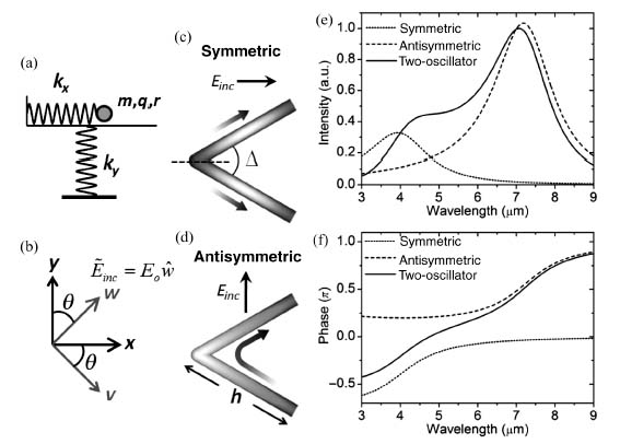
We focus on lithographically defined nanoscale V- and Y-shaped plasmonic antennas as examples of two-oscillator systems. These antennas exhibit two noninteracting plasmonic modes, each of which can be treated as an independent oscillator. We choose our axes such that the two oscillators are oriented along x- and y-axes, respectively, with the incident light propagating along z and its electric field oriented along an axis w, which lies in the x–y plane at an angle θ from the y-axis (Fig. 6.3b). According to Equation 6.4 the fields scattered by the oscillators oriented along the x- and y-axes can be written respectively as
(6.6) 
(6.7) 
where  contains the angular and radial dependence of the emitted field. In general, light is scattered by our two-oscillator element into some elliptical polarization state. We focus on light scattered only into the polarization state along the v-axis in Figure 6.3b, which is the cross-polarized direction relative to the incident polarization. The reason for this particular choice is twofold. The first is a matter of experimental convenience as it allows us to fully decouple the scattered light from the incident light by simply filtering out the former with a linear polarizer. The second is more subtle; as we will show, this configuration provides an additional phase shift which extends the potential phase coverage of our elements to the full 2π range.
FIGURE 6.3 (a) Charge-oscillator model for a two-oscillator element, where q is the charge and m is the inertial mass. (b) Two coordinate systems related by a rotation by angle θ. The x–y axes are along the two fundamental oscillator modes, the w-axis is along the polarization of the incident field, and the v-axis is along the cross-polarization direction with respect to the incident polarization. A V-shaped optical antenna is a simple example of a plasmonic two-oscillator element. Its two orthogonal modes, that is, symmetric and antisymmetric modes, are shown, respectively, in (c) and (d). The schematic current distribution on the antenna is represented in gray scale with lighter tones indicating larger current density. The instantaneous direction of current flow is indicated by arrows with gradient. (e) Calculated intensity (|E|2) of the field scattered into the cross-polarization by individual oscillators representing the two modes of a V-shaped antenna (dashed and dotted curves) with Δ = 90° and h = 650 nm and by the two-oscillator system representing the V-antenna (solid curve) for θ = 45°. Note that the solid curve is not simply the sum of the dashed and dotted curves because of the coherent addition of fields. (f) Phase of the field scattered into the cross-polarization by the individual oscillators (dashed and dotted curves) and by the two-oscillator system (solid curve).
Given an incident field polarized along the w-axis (Fig. 6.3b), we wish to study the component of the emitted field polarized along the v-direction Es, v(ω). We can break up this polarization conversion process into two steps: the in-coupling of incident light into the two oscillator modes and the out-coupling of cross-polarized light from the oscillators. The in-coupling process depends on θ because it involves the projection of the incident field along the two oscillator modes, that is,  and
and  For the out-coupling process, we project the field scattered by each oscillator onto the v-axis (Fig. 6.3b):
(6.8) 
(6.9) 
After summing these projections, the total cross-polarized field emitted by the structure Es, v can be written as
where we assumed that  which is true for light emitted approximately normal to the orientation of the two oscillators. Equation 6.10 provides a complete description of the generation of cross-polarized light by our two-oscillator system.
A large class of plasmonic elements can support two orthogonally orientated modes. We choose V-shaped antennas consisting of two arms of equal length h connected at one end at an angle Δ. They support “symmetric” and “antisymmetric” modes (Figs. 6.3c and 6.3d), which are excited by electric field components parallel and perpendicular to the antenna symmetry axis, respectively. In the symmetric mode, the current and charge distributions in the two arms are mirror images of each other with respect to the antenna's symmetry plane, and the current vanishes at the joint that connects the two arms (Fig. 6.3c). This means that, in the symmetric mode, each arm behaves similarly to an isolated rod antenna of length h, and therefore the first-order antenna resonance occurs at h ≈ λeff/2, where λeff is the effective wavelength [2]. In the antisymmetric mode, antenna current flows across the joint (Fig. 6.3d). The current and charge distributions in the two arms have the same amplitude but opposite sign, and they approximate those in the two halves of a straight rod antenna of length 2h, and the condition for the first-order resonance of this mode is 2h ≈ λeff/2. The calculations of Figure 6.3e indeed show that the two modes differ by about a factor of 2 in resonance wavelength.
The calculated intensity |Es, v(ω)|2 and phase  (ω) of the cross-polarized light Es, v(ω) = |Es, v(ω)|ei
 (ω) for a representative V-antenna are plotted in Figures 6.3e and 6.3f. The specific parameters Γa, i, Γs, i, mi, ω0, i (i
  x, y) for its two modes correspond to antenna geometries specified in the caption of Figure 6.3. As can be clearly seen from the solid curve in Figure 6.3f, our two-oscillator element is able to span twice the range of phase of either single oscillator (dashed or dotted), even though the two oscillators are uncoupled. This phase extension, which can be seen as the eiπ term in Equation 6.10, is due to the fact that the projections of the scattered fields from the spatially overlapped x- and y-oriented oscillators onto the v-axis are opposite in phase (Fig. 6.3b).
Equation 6.10 encodes the θ-dependence of the polarization conversion properties with a sin(2θ) term. No cross-polarized light is generated for θ = 0° or 90° when the incident field is aligned along one of the two orthogonally oriented modes, and maximum polarization conversion is obtained for θ = 45°. A feature of the two-oscillator element is that the rotation of both oscillators relative to the incident polarization allows for control of the scattering amplitude independent of the phase response or the line width of the resonances. Within the 0°–90° range, the θ-dependence in Equation 6.10 only affects the amplitude of Es, v, so θ can be used as a degree of freedom to control the cross-polarized scattering amplitude of the two-oscillator element without altering its phase response. Due to the sin(2θ) dependence, a rotation of the structure by 90° maintains the amplitude of cross-polarized scattering while adding an extra phase of π to the scattered light. This feature is used later to generate 8 distinct phase elements from 4 structures and allows us to construct antenna elements that are able to span the full 0-to-2π range in phase, while maintaining relatively large scattering amplitudes.
6.1.4 Analytical Models for V-Shaped Optical Antennas
In this section, we present the results of analytical models for solving the current distribution and scattered fields of V-shaped antennas and in doing so obtain a detailed picture of their near- and far-field properties. In particular, we are able to study the near-field coupling between the two antenna arms, and accurately map the amplitude, phase, and polarization of the antenna radiation in arbitrary directions. The convenient modeling tools enable us to select and assemble various V-shaped antennas into more complex optical systems.
Models describing the response of antennas have been extensively studied [28, 45–47]. One of the main challenges is that the integral equations governing the behavior of antennas have no exact analytical solutions. However, the integral equations can be solved in an approximate way by following an iteration procedure developed in 1950s by King [28]. Furthermore, with the development of numerical methods in the last few decades, we can obtain accurate numerical solutions of the integral equations in an efficient manner following the method of moments (MoM). We present in the Appendix of this chapter the integral equations for V-antennas, as well as the iteration method and the MoM used to calculate the antenna behavior. We study how the methods and approximations used for long wavelengths apply to the mid-infrared spectral range, where plasmonic properties play a significant role, by comparing the results of our analytical models with the results of FDTD simulations. Our main goal here was to propose fast and efficient methods as alternatives to full-wave simulations to probe a large design parameter space, bringing techniques commonly used in the microwave and radio frequency ranges to the attention of the optics community.
Our solutions follow the derivations presented in Reference 28 for solving Hallén's integral equation using the iteration method and in Reference 47 for solving Pocklington's integral equation using the MoM. We first derive the integral equations governing the behavior of V-shaped cylindrical antennas, reduce the 2D problem to one dimension, and implement a numerical solution based on the iteration method or the MoM. We obtain the current distribution driven at the surface of the antenna by an incident excitation field. The far field scattered by the antenna in any direction, with amplitude, phase, and polarization information, is then calculated as the coherent sum of the fields scattered by a series of infinitesimal current elements distributed along the antenna and having their amplitude and phase given by the current distribution, using an analytical expression for the radiation pattern of interfacial dipoles [48].
The main approximation used in our derivations is the thin-wire approximation (a << λo and a << h, with a being the antenna radius and h its arm length) which enables us to consider the current distribution on the antenna to be purely axial and azimuthally invariant [46, 47]. While fully justified at long wavelengths, this approximation may seem crude for mid-infrared antennas for which typically λo/a ∼ 50 and h/a ∼ 10. Our first task is thus to validate our results by comparing them to the results of well-established simulation tools such as FDTD. We assume monochromatic light at λo = 7.7 μm coming at normal incidence with respect to the antenna plane. We calculated the amplitude and phase of the scattered light in the far field, in the direction normal to the plane of the antenna, for different antenna arm lengths h, ranging from 0.3 to 1.6 μm, and different opening angles Δ, ranging from 0° to 180°. The results are summarized in Figure 6.4 for the symmetric and antisymmetric plasmonic modes (see inset schematics). We observe a good agreement between FDTD calculations and our calculations based on the MoM and iteration method. The locations of the two modes are different with respect to h because the physical length of the antenna for the two modes differs by a factor of 2. We also observe a phase shift approximately equal to π across the resonances, as is expected across any resonance. We note that our calculations are in good agreement with FDTD simulations for Δ < 90°, where the shift of the resonance peaks occurs, indicating that the near-field interactions between the antenna arms are well accounted for in our analytical models. These maps were obtained in about 20 s using the MoM and about half an hour using the iteration method on a desktop computer, compared to about 1 month for the FDTD calculations.
FIGURE 6.4 The first, second, and third rows are, respectively, FDTD simulations, method of moments (MoM) calculations, and calculations following King's iteration method of the amplitude and phase responses of V-antennas. The first and third columns are the amplitudes of the scattered light (|E|) as a function of the antenna arm length h and the angle between the antenna arms Δ, for the antisymmetric and the symmetric modes, respectively. The second and fourth columns are the phases of the scattered light for the antisymmetric and the symmetric modes, respectively. The arrows indicate the orientation of the two antenna modes.
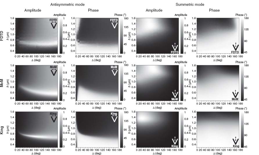
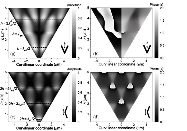
Figure 6.5 shows the current distributions on the antenna (in curvilinear coordinates) as a function of arm length h for the symmetric modes with Δ = 45° (a and b) and for the antisymmetric modes with Δ = 135° (c and d). We observe that the antenna resonances occur when the physical length of the antenna equals an odd integer multiple of half effective wavelength, that is, h ≈ Nλo/(2neff) for the symmetric modes and 2h ≈ Nλo/(2neff) for the antisymmetric modes, where N = 1, 3, 5, … Interestingly, we also observe “forbidden” resonances when the antenna length equals an integer multiple of the effective wavelength, that is, h ≈ Nλo/neff, for the symmetric modes when Δ is small (Fig. 6.5a). In straight rod antennas, these resonances feature symmetric charge distributions (e.g., + – +) along the antenna axis and cannot be excited by plane waves [49, 50]. In the case of our V-antennas, the coupling between the two arms breaks this symmetry so these “forbidden” resonances can be optically addressed.
FIGURE 6.5 (a) Amplitude and (b) phase of the current along an antenna with opening angle Δ = 45° and antenna arm length h varying from 0.3 to 5 μm. The incident electric field is polarized along the symmetry axis. The incident wavelength is λo = 7.7 μm. (c) and (d) are similar to (a) and (b) for an incident electric field polarized perpendicular to the antenna symmetry axis and for an opening angle Δ = 135°.
6.1.5 Optical Properties of V-Shaped Antennas: Experiments and Simulations
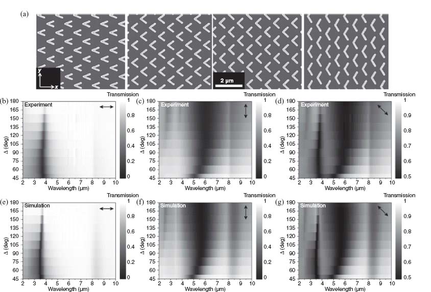
We characterize the spectral response of these antennas by Fourier transform infrared (FTIR) spectroscopy and numerical simulations. In Figure 6.6, we mapped the two oscillator modes of V-shaped antennas as a function of wavelength and opening angle Δ by showing the measured (b–d) and calculated (e–g) transmission spectra. The gold antennas fabricated on silicon wafers have arm length h = 650 nm, width w = 130 nm, thickness t = 60 nm, and opening angle ranging from 45° to 180°. The orientation of the incident polarization is shown in the upper right corner. Figures 6.6b and 6.6e correspond to excitation of only the x-oriented symmetric antenna mode, whereas Figures 6.6c and 6.6f correspond to the y-oriented antisymmetric mode and Figures 6.6d and 6.6g show both excited modes. The spectral position of these resonances are slightly different from the first-order approximation which would yield λx ≈ 2hneff ≈ 3.4 μm and λy ≈ 4hneff ≈ 6.8 μm, taking neff as 2.6 [15–17], with the differences attributed to the finite aspect ratio of the antennas and near-field coupling effects, which are especially strong for small Δ when the arms are in closer proximity to each other, leading to a significant resonance shift (Figs. 6.6c and 6.6f). All of the results of the experiment are reproduced very well in simulations, including the feature at 8–9 μm due to a phonon resonance in the 2 nm native silicon oxide layer on the silicon substrate, which is enhanced by the strong near fields formed around the metallic antennas. In Figures 6.6c, 6.6d, 6.6f), and 6.6g, a higher order antenna mode is clearly visible at λo ≈ 2.7 μm for large Δ.
FIGURE 6.6 (a) SEM images of gold V-shaped antennas fabricated on a silicon substrate with opening angles Δ = 45°, 75°, 90°, and 120° from left to right. (b–d) Measured transmission spectra through the V-antenna arrays at normal incidence as a function of wavelength and angle Δ for fixed arm length h = 650 nm. The incident light is polarized (b) along the symmetry axis of the antennas, (c) perpendicular to the symmetry axis, and (d) at a 45° angle. (e–g) FDTD simulations corresponding to the experimental spectra in (b–d), respectively. The feature at λo = 8–9 μm is due to the phonon resonance in the ∼2 nm SiO2 on the substrate.
We measured the generated cross-polarization using our FTIR setup in transmission mode, inserting a polarizer after the sample at 90° to the incident polarization. The resulting spectra for incident polarization 45° from the x-axis (Fig. 6.6a), normalized to the light directly transmitted through the bare silicon substrate, are shown in Figure 6.7a. As expected, the polarization conversion peaks in the 3–8 μm range, in the vicinity of the two antenna resonances. The corresponding FDTD simulations are shown in Figure 6.7b and retain the same features as the experiment, though the simulated polarization conversion spectra are more clearly broken up into two resonances. The experimental data show less of this separation probably because of inhomogeneous broadening in the experiment due to fabrication imperfections, non-normal incident angle in our FTIR-microscope setup (numerical aperture of the microscope lens is ∼0.4), and limited coherence area of our thermal source.
FIGURE 6.7 Experimental measurements (a), FDTD simulations (b), and MoM calculations (without considering the absorption of the SiO2 layer on the silicon substrate) of the cross-polarized scattering for the V-antenna arrays in Figure 6.6. The arrows indicate the polarization of the incident and output light.

6.2 APPLICATIONS OF PHASED OPTICAL ANTENNA ARRAYS
6.2.1 Generalized Laws of Reflection and Refraction: Meta-Interfaces with Phase Discontinuities
In this section, we show one of the most dramatic demonstrations of controlling light using the tuneable phase shift between the emitted and incident radiation of optical resonators; that is, a linear phase variation along an interface introduced by an array of phased optical antennas leads to anomalously reflected and refracted beams in accordance with generalized laws of reflection and refraction.
The propagation of light is governed by Fermat's principle, which states that the trajectory taken between two points A and B by a ray of light is that of least optical path,  where
where  is the local index of refraction. Light chooses this least path from point A to B because it lies at an extremum, where the derivative of the optical path length, or equivalently the accumulated optical phase
  with respect to infinitesimal variation of the path, is zero. Light waves that stay close to the variationally stable path arrive at their destination with nearly the same phase and therefore interfere constructively. In this sense, Fermat's principle can be stated as the principle of stationary phase [51–53]. Now suppose an abrupt phase shift
  is introduced in the optical path by suitably engineering the interface between two media;
  depends on the coordinate
  along the interface. Then the total phase shift
  must be stationary for the actual path that light takes. This allows us to revisit and generalize the laws of reflection and refraction.
Consider an incident plane wave at an angle θi. Assuming that the two paths are infinitesimally close to the actual light path (Fig. 6.8), then the phase difference between them is zero:
(6.11) 
where θt is the angle of refraction, Φ and Φ + dΦ are, respectively, the phase shifts at the locations where the two paths cross the interface, dx is the distance between the intersections, and ni and nt are the refractive indices of the two media. If the phase gradient along the interface is designed to be constant, the previous equation leads to the generalized Snell's law of refraction:
FIGURE 6.8 Schematics used to derive the generalized Snell's law of refraction. The interface between the two media is artificially structured in order to introduce an abrupt phase shift in the light path, which is a function of the position along the interface. Φ and Φ + dΦ are the phase shifts where the two paths cross the boundary.
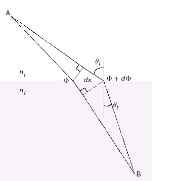
Equation 6.12 implies that the refracted ray can have an arbitrary direction, provided that a suitable constant gradient of phase discontinuity along the interface (dΦ/dx) is introduced. Because of the nonzero phase gradient in this modified Snell's law, the two angles of incidence ±θi lead to different values for the angle of refraction. As a consequence, there are two possible critical angles for total internal reflection, provided that nt < ni:
Similarly, for the reflected light we have
where θr is the angle of reflection. There is a nonlinear relation between θr and θi, which is dramatically different from conventional specular reflection. Equation 6.14 predicts that there is always a critical incidence angle
(6.15) 
above which the reflected beam becomes evanescent.
As shown in previous sections, the phase shift between the scattered and the incident radiation of an optical antenna changes appreciably across a resonance. By spatially tailoring the geometry of the antennas in an array and hence their phase response, one can design the linear phase shift along the interface and mold the wavefront of the reflected and refracted beams in nearly arbitrary ways. The spacing between the antennas in the array should be subwavelength to provide efficient scattering and to prevent the occurrence of grating diffraction. However, it should not be too small to introduce strong near-field coupling between neighboring antennas that will perturb their phase responses. Note that due to the discreteness in our approach to approximate the linear phase distribution, in general there will always be regularly reflected and refracted beams, which follow conventional laws of reflection and refraction (i.e., dΦ/dx = 0 in Eqs. 6.12 and 6.14). The antenna packing density controls the relative amount of energy in the anomalously reflected and refracted beams.
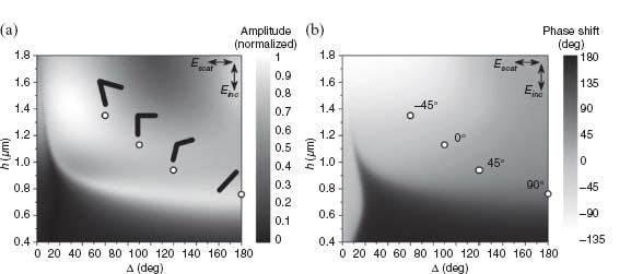
Figure 6.9 shows the amplitude and phase responses of gold V-antennas calculated using the iteration method previously discussed. The antenna symmetry axis is along 45° direction so that both the symmetric and antisymmetric plasmonic modes are excited, given a vertical incident polarization (Fig. 6.9a inset). As a result of the modal properties of the V-antennas and the degrees of freedom in choosing antenna geometry (h and Δ), the cross-polarized scattered light can have a large range of amplitudes and phases for a given wavelength λo = 8 μm. We chose four antennas indicated by circles in Figure 6.9, which provide an incremental phase of π/4 from left to right and almost equal scattering amplitudes for the cross-polarized scattered light.
FIGURE 6.9 Analytically calculated amplitude (a) and phase shift (b) of the cross-polarized scattered light for gold V-antennas at λo = 8 μm. The four circles in the figures indicate the values of h and Δ used in experiments.
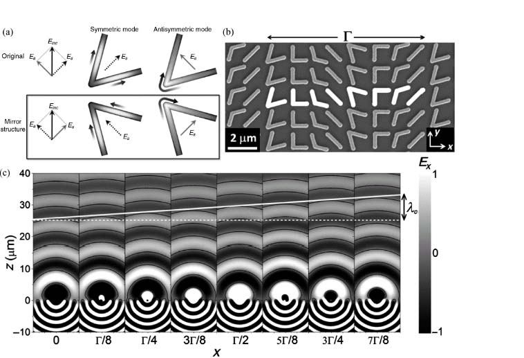
Phase shifts covering the entire 0-to-2π range are needed to provide full control of the wavefront. We take the mirror structure (Fig. 6.10a, lower panel) of an existing V-antenna (Fig. 6.10a, upper panel) (or rotate the original antennas clockwise by 90°) so that the cross-polarized emission has an additional π phase shift. This is evident by observing that the currents leading to cross-polarized radiation are π out of phase in the two panels of Figure 6.10a. A set of eight antennas are thus created from the initial four antennas shown in Figure 6.9, and by periodically arranging these eight antennas we created meta-interfaces that can imprint a linear phase shift to the optical wavefronts. A representative fabricated sample with the densest packing of antennas is shown in Figure 6.10b. FDTD simulations confirm that the amplitudes of the cross-polarized radiation scattered by the eight antennas are nearly equal with phases in π/4 increments (Fig. 6.10c). The periodic antenna arrangement is used here for convenience, but is not necessary to satisfy the generalized laws of reflection and refraction. It is only necessary that the phase gradient is constant along the plasmonic interface and that the scattering amplitudes of the antennas are all equal. The phase increments between nearest neighbors do not need to be constant, if one relaxes the unnecessary constraint of equal spacing between nearest antennas.
FIGURE 6.10 (a) V-antennas (upper panel) and their mirror structures (lower panel). The horizontal components of the scattered electric field in the two cases have a π phase difference. (b) SEM image of a meta-interface consisting of a phased optical antenna array fabricated on a silicon wafer. The meta-interface can introduce a linear phase distribution along the interface and is used to demonstrate the generalized laws of reflection and refraction. The unit cell of the structure (highlighted) comprises eight gold V-antennas of width ∼220 nm and thickness ∼50 nm and it repeats with a periodicity of Γ = 11 μm in the x-direction and 1.5 μm in the y-direction. The antennas are designed to have equal scattering amplitudes and constant phase difference ΔΦ = π/4 between neighbors. (c) FDTD simulations of the scattered electric field for the individual antennas composing the unit cell. Plots show the scattered electric field polarized in the x-direction for y-polarized plane wave excitation at normal incidence from the silicon substrate. The silicon substrate is located at z ≤ 0. The antennas are equally spaced at a subwavelength separation Γ/8, where Γ is the unit cell length. The tilted white solid line is the envelope of the projection on the x–z plane of the spherical waves scattered by the antennas. On account of Huygens' principle, the anomalously refracted beam resulting from the superposition of these spherical waves is then a plane wave that satisfies the generalized Snell's law (Eq. 6.12) with a phase gradient |dΦ/dx| = 2π/Γ along the interface.
We used a setup like the schematics shown in Figure 6.11a to demonstrate the generalized laws of reflection and refraction. Large arrays (∼230 μm × 230 μm) like the one shown in Figure 6.10b were fabricated to accommodate the size of the plane-wave-like excitation (beam radius ∼100 μm). Figure 6.11b summarizes the experimental results of ordinary and anomalous refraction for six samples with different Γ at normal incidence. The sample with the smaller Γ corresponds to larger phase gradient and more efficient light scattering into the cross-polarized anomalous beams. We observed that the angles of anomalous refraction agree well with theoretical prediction (Fig. 6.11b):
which is obtained by substituting –2π/Γ into Equation 6.12 for dΦ/dx and the refractive indices of silicon and air (nSi and 1) for ni and nt. Our FDTD simulations indicate that the scattering cross-sections σscat of the antennas range from 0.7 to 2.5 μm2, which is comparable to or smaller than the average area each antenna occupies, σaver (i.e., the total area of the array divided by the number of antennas). Therefore, it is reasonable to assume that near-field coupling between antennas will introduce only small deviations from the response of isolated antennas. Simulations also show that the absorption cross-sections σabs are ∼5–7 times smaller than σscat, indicating comparatively small ohmic losses in the antennas at mid-infrared wavelength range.
FIGURE 6.11 (a) Schematic experimental setup for y-polarized excitation (electric field normal to the plane of incidence). Angle of refraction and angle of reflection for the ordinary and anomalous beams, as well as angle of incidence, are labeled. (b) Measured far-field intensity profiles of the refracted beams for incidence normal to the interface. The gray and black curves are measured with and without a polarizer, respectively, for six samples with different Γ. The amplitude of the gray curves is magnified by a factor of three for clarity. The polarizer is used to filter out the anomalous refraction. The arrows indicate the calculated angles of anomalous refraction according to Equation 6.16. (c) Angle of refraction versus angle of incidence for the sample with Γ = 15 μm. The curves are theoretical calculations using the generalized Snell's law (Eq. 6.12) and the symbols are experimental data. The two arrows indicate the modified critical angles for total internal reflection. The shaded region represents “negative” refraction for the cross-polarized light as illustrated in the inset. (d) Angle of reflection versus angle of incidence for the sample with Γ = 15 μm. The upper left inset is the zoom-in view. The curves are theoretical calculations using Equation 6.14 and the symbols are experimental data. The arrow indicates the critical incidence angle above which the anomalously reflected beam becomes evanescent. The shaded region represents “negative” reflection for the cross-polarized light as illustrated in the lower right inset.
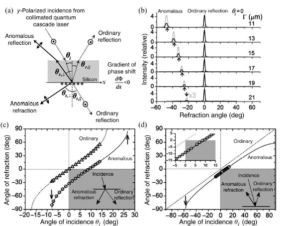
Figures 6.11c and 6.11d show the angles of refraction and reflection, respectively, as a function of θi for both the silicon–air interface and the meta-interface. In the range of θi = 0°–9°, the meta-interface exhibits negative angle of refraction and reflection for the cross-polarized scattered light (schematics are shown in the lower right insets of Figs. 6.11c and 6.11d). The critical angle for total internal reflection is modified to about –8° and +27° for the meta-interface in accordance with Equation 6.13 compared to ±17° for the silicon–air interface; the anomalous reflection does not exist beyond θi = –57°. We note that antenna arrays in the microwave and millimeter-wave regime have been used for the shaping of reflected and transmitted beams in the so-called reflectarrays and transmitarrays. There is a connection between that body of work and our results in that both use abrupt phase changes associated with antenna resonances. However, the generalization of the laws of reflection and refraction we present is made possible by the deep-subwavelength thickness of our optical antennas and their subwavelength spacing. It is this meta-surface nature of the plasmonic interface that distinguishes it from reflectarrays and transmitarrays, which typically consist of a double-layer structure separated by a dielectric spacer of finite thickness, and the spacing between the array elements is not subwavelength.
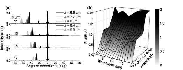
The antenna designs in Figure 6.10b are broadband; that is, they provide approximately 0-to-2π phase coverage with approximately π/4 intervals over a wide range of wavelengths. Figure 6.12a shows experimental results of ordinary and anomalous refraction for normally incident light at five different wavelengths. There are four samples with unit cell length Γ ranging from 11 to 17 μm, corresponding to different phase gradients. For all samples and all excitation wavelengths, we observe anomalously refracted beams away from the surface normal by an angle –arcsin(λo/Γ), predicted by the generalized laws. Most importantly, we see negligible intensity at +arcsin(λo/Γ), indicating that the interfaces operate in the metamaterial regime and do not function like a grating with periodicity Γ. The reason for this broadband behavior can be understood by looking at the phase responses of the eight constituent antennas (Fig. 6.12b). Although the antennas were designed to generate anomalous beams at λo = 8 μm, their phase responses, in terms of both the total phase coverage and the incremental phase between neighbors, do not vary significantly over a large range of wavelengths from λo = 6 to 14 μm.
FIGURE 6.12 (a) Experimental results showing anomalous refraction (located at θt < 0) from meta-interfaces with various phase gradients (from 2π/11 to 2π/17 μm) at different wavelengths (from 5.5 to 9.9 μm), as well as the ordinary refraction (located at θt = 0), given normal incidence excitation. (b) FDTD simulations of the phase responses of the eight antennas in Figure 6.10b at wavelengths ranging from 4 to 20 μm. The phase response is roughly linear from 0 to 2π for wavelengths from λo = 6 to 14 μm. The phase response of the first antenna is used as the reference, which is set to be zero.
6.2.2 Out-of-Plane Reflection and Refraction of Light by Meta-Interfaces
A key feature of the conventional laws of reflection and refraction is that the incident, reflected, and transmitted beams lie in the same plane, that is, the plane of incidence. Recent research on metamaterials and in particular on left-handed optical materials has shown that even if light can be refracted in unusual ways, the refraction angle is still described by the traditional form of Snell's law, albeit with a negative index of refraction [54–58]. In this section, we derive laws of reflection and refraction in three dimensions, applicable to the case in which the interfacial phase gradient does not lie in the plane of incidence, leading to the remarkable features of out-of-plane reflection and refraction [19].
We use the principle of stationary phase to derive the 3D reflection and refraction laws. Suppose the two paths in Figure 6.13a are infinitesimally close to the actual optical path. We shall have  where the integrals are along the paths through point A and B on the interface, respectively. The equation can be rewritten as
where  is the wavevector of light in the medium of index ni (nt) and
  is the position of A (B) on the x–y plane. For constant phase gradients, the accumulated phase of rays intersecting the interface is a convex downward function for all values of x and y [59], so we can rewrite the stationary phase condition in Equation 6.17 for the x and y spatial coordinates independently:
FIGURE 6.13 Schematics used to describe the generalized refraction at an interface with arbitrary orientation of the phase gradient. (a) The interface between two media of refractive index ni and nt is structured to introduce a constant interfacial phase gradient  Two points, Pi and Pt, are located, respectively, in mediums 1 and 2. The difference of the phase accumulated along two paths from Pi to Pt that are infinitesimally close to the actual optical path is zero according to Fermat's principle of stationary phase. (b and c) The projection of the incident wavevector on the interface
  forms a nonzero angle with the direction of the interfacial phase gradient. As a result during the interaction with the meta-interface, the light beams acquire a k-vector component equal to the phase gradient
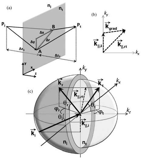
Note that due to the lack of translational invariance along the interface the tangential wavevector of the incident photon is not conserved; the interface contributes an additional “phase matching” term equal to the phase gradient. By considering two infinitesimally close paths separating two points located in the same medium one can immediately see that similar equations hold for the wavevector components kx, r and ky, r of the reflected beam.
Without loss of generality, we choose the coordinate system such that  lies in the y–z plane (the plane of incidence), that is, kx, i = 0 (Fig. 6.13b). Equation 6.18 shows that it is no longer possible to define a plane that contains the incident, reflected, and transmitted beams. The usual planar k-space representation used to illustrate refraction and reflection needs to be extended into three dimensions. The angle of reflection (refraction) is now given by the wavevector that satisfies the tangential wavevector relation (Fig. 6.13b) and intersects the k-sphere in the medium 1 (2) of radius k = ni ko (k = nt ko). A schematic of this new physical situation is presented in Figure 6.13c. This 3D geometrical k-space representation is widely used to describe electron, neutron, and X-ray diffraction and is known in the literature as Ewald's sphere [60].
The directions of the reflected and refracted wavevectors are characterized by the angles θr(t) (the angle between  and its projection on the x–z plane) and
  r(t) (the angle formed by the projection of
  on the x–z plane and the z-axis), as defined in Figure 6.13c. With this choice of notation, we obtain the generalized law of reflection in 3D,
(6.19) 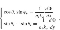
and the generalized law of refraction in 3D,
Notice that when the phase gradient is oriented along the plane of incidence (dΦ/dx = 0) the anomalous reflection and refraction are in plane and one recovers Equations 6.12 and 6.14. The nonlinear nature of these equations is such that two different critical angles now exist for both reflection and refraction. When a ray of light traverses an interface, it will propagate in the new medium as long as its longitudinal wavevector kz remains real. This implies that the tangential components of the k-vector have to be smaller than the modulus of the k-vector in the medium. When a phase gradient along the interface provides an additional tangential component of the k-vector, the condition for the existence of a transmitted or reflected propagating beam is changed. From Equation 6.20, we can find the condition for kz, t to be zero (φt = 90°), leading to the expression for two critical angles for refraction:
(6.21) 
Note that a critical angle for refraction may exist even when ni < nt for some interfacial phase gradients. For reflection, the nonlinear relation between θr and θi yields two critical angles for reflection:
(6.22) 
We experimentally observed out-of-plane refraction in accordance with the new 3D law (Eq. 6.20) using an interface patterned with phased optical antenna arrays oriented in such a way that the interfacial phase gradient forms an angle α with respect to the plane of incidence (Fig. 6.14).
FIGURE 6.14 Schematic representation of the reflection and refraction of light in three dimension. The incident light from a collimated quantum cascade laser emitting at λo = 8 μm impinges at an angle θi with respect to the z-axis on an interface between silicon and air. The incidence is from silicon and the polarization of the incident light is maintained so that it forms an angle of 45° with respect to the two plasmonic modes of the antennas. The sample is the same as that used in Figure 6.10b. When the interfacial phase gradient  imposed by the V-antenna arrays is not parallel to the y-axis, a component of the phase gradient out of the plane of incidence is created, resulting in out-of-plane anomalous beams satisfying the 3D laws of reflection and refraction (Eqs. 6.19 and 6.20).
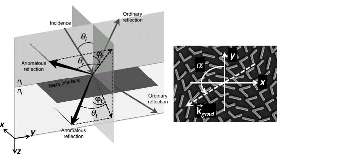
We studied both the ordinary and anomalous refraction for various incidence angles and various phase gradient orientations. The magnitude of the phase gradient is fixed to dΦ/dr = 2π/15 (radian/μm) for all the experiments. The experimental results are summarized in Figure 6.15b and unambiguously show out-of-plane refraction that agrees well with the prediction of Equation 6.20. Figure 6.15a shows measured far-field intensity distribution for a phase gradient perpendicular to the plane of incidence.
FIGURE 6.15 Experimental observation of out-of-plane refraction. (a) Measured far-field intensity as a function of the angular position of the detector θ and φ (defined in a similar way as θt and φt in Fig. 6.14) for a laser beam incident on the interface from the silicon side at an angle θi = –8.45° and for a phase gradient perpendicular to the plane of incidence. As expected, the ordinary refracted beam is in plane (φ = 0°) at an angle following the conventional Snell's law, that is, θ = –30°. The anomalous beam is refracted out of plane at angles φ = –38° and θ = –30°. The inset shows the angular distribution of the intensity at a fixed angle φ = –38° (light curve) and at a fixed angle θ = –30° (dark curve). (b) Angles of refraction versus angles of incidence and orientations of phase gradient α. Curves are theoretical calculations based on the 3D Snell's law (Eq. 6.20). Circles are experimental data.
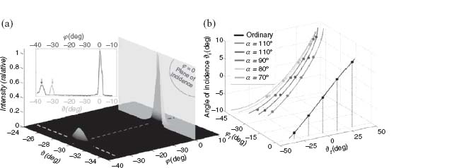
In summary, 3D laws of reflection and refraction are derived for optically thin meta-interfaces that impart to the incident wavefront a phase gradient arbitrarily oriented with respect to the plane of incidence. Due to the tangential wavevector provided by the anisotropic interface, the incident beam and the anomalously reflected and refracted beams are in general non-coplanar and two different critical angles exist for both reflection and refraction. The beams' direction can be controlled over a wide range by varying the angle between the plane of incidence and the phase gradient. Experiments on arrays of subwavelength optical antennas demonstrate out-of-plane refraction in excellent agreement with the 3D Snell's law, illustrating the unique beaming capabilities of meta-interfaces at optical frequencies.
6.2.3 Giant and Tuneable Optical Birefringence
We have shown that the optical properties of V-antennas, and in general any 2D plasmonic structures that support two charge-oscillation eigenmodes, can be captured by a simple model involving two independent, orthogonally oriented harmonic oscillators. We show in this section that meta-interfaces consisting of V- and Y-shaped plasmonic antennas exhibit widely tailorable birefringence, where the optical anisotropy can be controlled by interference between the light scattered by the two plasmonic eigenmodes of the antennas.
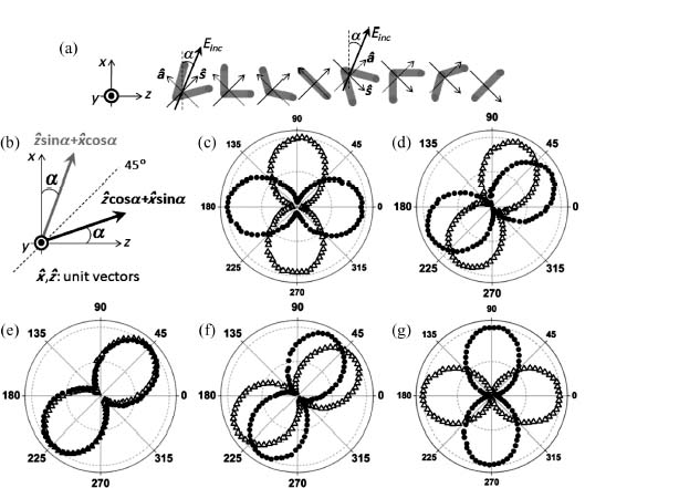
We studied the birefringence properties of the meta-interfaces shown in Figure 6.10b by changing the incident polarization at normal incidence so that the two orthogonal plasmonic modes are excited with different amplitudes, leading to a rotation of the polarization of the scattered light. Assume that the angle between the incident polarization and the x-axis is α and the symmetry axes of the eight antenna elements are 45° away from the vertical direction (Fig. 6.16a). We decompose the incident electric field into components that drive the symmetric and antisymmetric modes, respectively (i.e., parallel and perpendicular to the antenna symmetry axis), and calculate the scattered light based on the amplitude and phase responses of the two modes. Theoretical analysis shows that the scattered light contains two contributions that are polarized along the α-direction and (90° – α)-direction, respectively (Fig. 6.16b). The (90° – α)-polarized components of all eight antennas have the same amplitude and incremental phase of π/4, which give rise to an anomalously refracted beam. The α-polarized components, however, do not have the same amplitude and the proper phase relation between neighboring antennas, which lead to a beam that propagates in the same direction as the ordinary refraction, as well as a small optical background over a large angular range. These birefringence properties of the meta-interface are experimentally confirmed at λo = 8 μm, and Figures 6.16c–6.16g show measured intensity of the ordinarily and the anomalously refracted beams as a function of the rotation angle of a linear polarizer located in front of the detector for different incident polarizations. The “eight” patterns in the figures indicate that both beams are linearly polarized, and that the polarizations of the ordinary and anomalous refraction are symmetric with respect to the 45° direction.
FIGURE 6.16 (a) Schematics of the eight-antenna unit cell and the incident polarization. The antenna symmetry axes, ŝ, are 45° from the vertical direction. (b) For incident polarization along the α-direction, the scattered fields from the antennas contain two components, directed along the gray and black arrows, respectively. Only the latter has the properly engineered phase response, that is, π/4 phase difference between neighbors, which leads to anomalously refracted beams polarized along the (90° – α)-direction. (c–g) Measured intensity of the ordinarily and anomalously refracted beams (triangles and dots, respectively) as a function of the rotation angle of a linear polarizer located in front of a detector (α = 0°, 30°, 45°, 60°, and 90° from (c) to (g)). The free-space wavelength is 8 μm.
The spectral position of the two plasmonic modes of V-antennas can be tuned by varying the arm length h and, to a smaller extent, by adjusting the opening angle Δ (Fig. 6.9). However, both of these simultaneously shift the resonance frequencies of the symmetric and antisymmetric modes of the antenna. By appending a “tail” to the V-antenna as shown in Figure 6.17a, an additional degree of freedom is attained that allows for independent tuning of the spectral position of the symmetric mode [17]. By increasing the tail length, hT, the symmetric mode is red-shifted without affecting the antisymmetric mode. This is confirmed by mapping out the two plasmonic modes for four different values of hT, by measuring the reflection spectra from arrays of these antennas (Figs. 6.17b and 6.17c) and by FDTD simulations (Figs. 6.17f and 6.17g).
FIGURE 6.17 Y-shaped plasmonic antennas. (a) SEM image of the antenna array. (b and c) Measured normal incidence reflectivity spectra of the symmetric and antisymmetric antenna modes, respectively, as a function of tail length hT, which varies from 100 nm to 700 nm by increments of 200 nm. The reflectivity of the bare silicon substrate is ∼0.3. The vertical dashed line shows that for hT = 500 nm the two modes are overlapping. The arrows in the insets indicate the polarization of the incident field. (d) Polarization conversion spectrum with incident polarization along 45°, with the incident and measured polarizations indicated with arrows. The polarization conversion is nearly extinguished for one intermediate value of hT. (e) Diagram explaining the extinguishment of polarization conversion due to destructive interference between contributions of the two antenna modes when hT is adjusted such that the two modes have the same resonant response. (f–h) FDTD simulations corresponding to the measurements in (b–d).
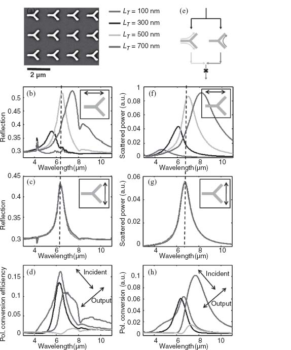
The measured polarization conversion efficiency of the Y-antennas is plotted in Figure 6.17d, given incident polarization along 45° with respect to the antenna symmetry axis, such that the projections of the incident field along the two antenna modes are equal. There is a substantial amount of polarization conversion for hT = 100, 300, and 700 nm. However, for hT = 500 nm, the polarization conversion is almost completely extinguished. FDTD simulations (Fig. 6.17h) demonstrate the same behavior as in the measurements. The origin of this effect can be interpreted as destructive interference between the contributions to the cross-polarization generation from the two oscillator modes. As illustrated in Figure 6.17e, the incident field excites both modes of the Y-antenna, each of which contributes to the cross-polarized field. However, as shown in Figure 6.3b, the projections of the emission of the two modes onto the v-axis are opposite in phase, so when the two modes are nearly identical in amplitude and phase responses (as is the case for hT = 500 nm), their contributions to the polarization conversion are π out of phase, resulting in destructive interference. In general, arrays of resonant structures which support two orthogonal plasmonic eigenmodes can be viewed as meta-interfaces with large and tuneable birefringence: They can rotate the polarization of light over a thickness of just tens of nanometers at optical wavelengths, and the degree of polarization rotation is controlled by the phase and amplitude responses of the two modes. This type of birefringence in anisotropic structures is referred to as “form birefringence” in literature (see, e.g., References 61–64).
6.2.4 Vortex Beams Created by Meta-Interfaces
To demonstrate the versatility of the concept of interfacial phase discontinuities, we fabricated meta-interfaces capable of creating vortex beams upon illumination by normally incident linearly polarized light [15, 18]. Optical vortices are a peculiar type of beams that have a doughnut-like intensity profile and a helicoidally shaped wavefront [65, 66]. Unlike plane waves for which the Poynting vector (or the energy flow) is always parallel to the propagation direction of the beam, the Poynting vector of a vortex beam follows a spiral trajectory around the beam axis (Fig. 6.18a). This circulating flow of energy gives rise to an orbital angular momentum [66].
FIGURE 6.18 (a–c) Wavefronts of optical vortex beams with topological charge l = 1, 2, and 3; l represents the number of twists of wavefront within a wavelength. (d) and (e) show common methods for characterizing an optical vortex. One can interfere the vortex beam with a diverging or converging Gaussian beam, producing a spiral interference pattern, as demonstrated in (d) by the spiral intersection between the wavefronts of the two beams. Alternatively, one can interfere the vortex beam with a plane wave, producing an interference pattern with dislocated fringes, schematically shown in (e).
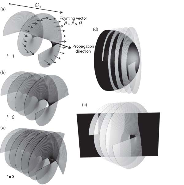
The wavefront of optical vortices has an azimuthal phase dependence, exp(ilθ), with respect to the beam axis. The number of twists, l, of the wavefront within a wavelength is called the topological charge of the beam and is related to the orbital angular momentum L of photons by the relationship L = ħl [66, 67], where ħ is the Planck's constant. Note that the polarization state of an optical vortex is independent of its topological charge. For example, a vortex beam with l = 1 can be linearly polarized or circularly polarized. The wavefront of the vortex beam can be revealed by a spiral interference pattern produced by the interference of the beam with the strongly curved spherical wavefront of a Gaussian beam (Fig. 6.18d). The topological charge can be identified by the number of dislocated interference fringes when the vortex beam and a plane-wave-like beam intersect with a small angle (Fig. 6.18e).
Optical beams with such helical phase profile are conventionally generated using spiral phase plates [68], SLMs [69], or holograms with fork-shaped patterns [70]. This type of beam can also be directly generated by lasers as an intrinsic transverse mode [71]. Optical vortices are of great fundamental interest since they carry optical singularities [65, 72] and can attract and annihilate each other in pairs, making them the optical analogue of superfluid vortices [73, 74]. Vortex beams are also important for a number of applications, such as stimulated emission depletion microscopy (STED) [75], optical trapping and manipulation [76, 77], and in optical communication systems, where the quantized orbital angular momentum can carry additional information [78, 79].
Figure 6.19 shows the experimental setup used to generate and characterize the optical vortices. It consists of a Mach–Zehnder interferometer where the optical vortices are generated in one arm and their optical wavefronts are revealed by interference with a reference Gaussian beam propagating through the other arm. A laser beam from a distributed feedback QCL emitting monochromatic light at λo = 7.75 μm in continuous wave mode with power of ∼10 mW is collimated and separated in two parts by a beam splitter. One part of the beam is rotated in polarization using a set of mirrors to serve as the reference beam. The second part is focused on a meta-interface phase mask using a ZnSe lens (20 inch focal length, 1 inch diameter). The phase mask comprises a silicon–air interface decorated with a 2D array of V-shaped gold plasmonic antennas designed and arranged so that it introduces a spiral shaped phase distribution to the scattered light cross-polarized with respect to the incident polarization. The inset SEM image of Figure 6.19 corresponds to l = 1. We chose a packing density of about 1 antenna per 1.5 μm2 (∼λo2/40), to maximize the efficiency of the device while avoiding strong near-field interactions. About 30% of the light power impinged on the meta-interfaces is transferred to the vortex beams.
FIGURE 6.19 Experimental setup based on a Mach–Zehnder interferometer used to generate and characterize optical vortices. The bottom inset SEM image shows a meta-interface phase plate with topological charge one. The plate consists of eight regions, each occupied by one of the eight elements in the unit cell in Figure 6.10b. The antennas are arranged to generate a phase shift that varies azimuthally from 0 to 2π, thus producing a helicoidal scattered wavefront.
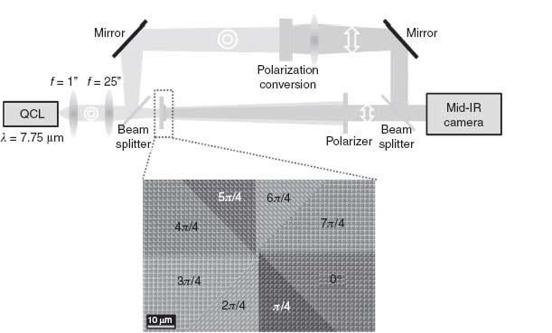
Figure 6.20a shows interferograms created by the interference between a plane-wave-like reference beam and the beam generated by the meta-interface while the two intersect with a small angle. The dislocation at the center of the interferograms confirms the presence of a phase defect at the core of the beam generated by the meta-interface. The orientation and the number of the dislocated fringes of the interferograms can be used to characterize the sign and the topological charge L of the vortex beam.
FIGURE 6.20 (a) Interferograms obtained from the interference between a plane-wave-like reference beam and optical vortices with different topological charges. The dislocation of the fringe pattern indicates the presence of a phase defect along the axis of the transmitted beam. Vortex beams with single (double) charge(s) are generated by introducing an angular distribution ranging from 0 to 2π (4π) using meta-interfaces. The azimuthal direction of the angular phase distribution defines the sign of the topological charge (also called chirality). (b) Spiral interferograms created by the interference of vortex beams and a co-propagating Gaussian beam.
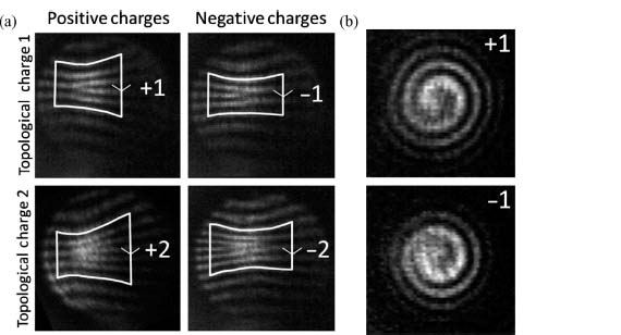
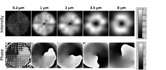
Figure 6.21 presents FDTD simulations of the evolution of the cross-polarized scattered field after a Gaussian beam at λo = 7.7 μm impinges normally on a 50 × 50 μm2 meta-interface phase plate like the one shown in Figure 6.19. We observe that a phase singularity, where the phase is undefined, is established at the center of the phase distribution as close as 1 μm (∼λo/8) away from the interface. The presence of such phase singularity produces the characteristic zero of intensity at the beam axis less than a wavelength away from the interface. The fact that a meta-interface molds the incident wavefront into an arbitrary shape almost instantaneously presents an advantage over conventional optical components, such as liquid-crystal SLM, which is optically thick, and diffractive optics, which require observers to be in the far-field zone characterized by Fraunhofer distance 2D2/λo, where D is the size of the element [59].
FIGURE 6.21 FDTD simulations of the cross-polarized scattered field as a function of distance from a meta-interface phase plate designed to create a single-charged optical vortex. The characteristic zero intensity at the center of the beam and the phase singularity develop as soon as the evanescent near-field components vanish, that is, about 1 μm or one-eighth of wavelength behind the interface.
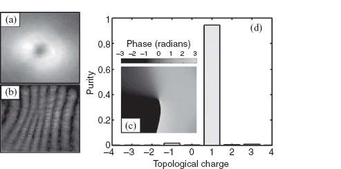
Meta-interfaces with discretized spiral phase distribution (e.g., the one shown in Fig. 6.19) are used and thus we are concerned about the quality of the optical vortex beams. We conducted a quantitative analysis of the generated optical vortices in terms of the purity of their topological charge. The amplitude distribution of the optical vortex is obtained from the measured intensity distribution (Fig. 6.22a), and its phase profile (Fig. 6.22c) is obtained by the recorded interferogram (Fig. 6.22b). The purity of the optical vortex is calculated by decomposing its complex field on a complete basis set of optical modes with angular momentum, that is, the Laguerre–Gaussian (LG) modes  [80]. The weight of a particular LG mode in the vortex beam is given by
  where Evortex is the complex electric field of the vortex beam, the star denotes complex conjugate, and the integers l and p are the azimuthal and radial Laguerre–Gaussian mode indices, respectively. The relative charge distribution of an optical vortex is obtained by summing all the modes with the same azimuthal index lo,
  A histogram representing the charge distribution for our vortex beam is plotted in Figure 6.22d. The purity of the single-charged vortex (l = 1) created with our technique is above 90%, similar to the purity of vortex beams obtained with conventional SLMs.
FIGURE 6.22 Analysis of the purity of the optical vortices generated by meta-interface phase masks. (a) Measured donut-shaped intensity profile of a vortex beam with l = 1. (b) Measured interferogram of the vortex beam when it interferes with a plane wave. The phase profile of the vortex beam in (c) is extracted via 2D Fourier and inverse Fourier transforms of the interferogram in (b), separating the vortex and reference beam in the Fourier space. (d) Histogram representing the decomposition of the single-charged vortex beam on a basis set of Laguerre–Gaussian modes with topological charge index lo.
In summary, this chapter discusses the phase response of plasmonic antennas and a new class of planar optical components, “meta-interfaces, ” which are based on phased optical antenna arrays. The control of phase response is achieved by choosing antenna geometry so it operates at different positions on the antenna resonance curve, corresponding to different phase shifts between the scattered and incident light. The meta-interface design features subwavelength control of phase, amplitude, and polarization of optical wavefront without relying on the propagation effect. This is very different from conventional optical components such as lenses, diffractive optics, and wave plates. The subwavelength resolution of meta-interface will enable not only far-field engineering but also near-field and meso-field engineering of optical wavefronts.
Assume the V-antenna is composed of two rods with length h and radius a, located in the x–z plane (Fig. 6.A.1). The angle between the two rods is Δ. One antenna rod, denoted No. 1, is aligned with z-axis, while the other, denoted No. 2, is aligned with s-axis. The wavevector of the linearly polarized incident light,  , lies in the symmetry plane of the V-antenna (light blue in Fig. 6.A.1A) and the angle between
  and the x–z plane is θ. The antenna response can be decomposed into a linear combination of two modes characterized by symmetric and antisymmetric current distributions in the two rods as discussed in the main text. The currents in the two rods satisfy
(6.A.2) 
where the superscripts “a” and “s” are used to distinguish the two modes. The boundary conditions at the ends and the joint of the V-antenna for the antisymmetric mode are
The latter states that the scalar potential is zero where the two rods join. This is due to antisymmetry, that is,  and electrical contact, that is,
  For the symmetric mode, we have
(6.A.5) 
The vector potential at the antenna joint is nearly zero because it is primarily determined by the current in the immediate vicinity of the joint (see Eqs. 6.A.8, 6.A.9, and 6.A.10), which is close to zero for the symmetric mode. For a better approximation, one can calculate the vector potential at the end of an isolated straight rod antenna of length h and use it to replace the zero at the right-hand side of Equation (6.A.6).
The boundary condition on the surface of the first rod reads
where  and
and  1 are the vector and scalar potentials on the surface of the rod, respectively; A1z is the z-component of
  ; β is free-space wavevector; and ω is angular frequency. Note that we have used the Lorentz gauge
  Equation 6.A.7 states that the tangential component of the electric field on the surface of the rod E1z is zero, which is valid for antennas made of perfect electric conductors. It can be generalized to account for antennas made of realistic metals, which will be discussed later. There are three contributions to the vector potential on the surface of an antenna rod: (1) that due to the current distribution on the rod itself (“self-interaction”), (2) that due to the current distribution on the other rod (“mutual interaction”), and (3) that due to the incident light. For example,
  is the z-component of the vector potential on the surface of the first antenna rod for the antisymmetric mode, where the three terms on the right-hand side represent the three contributions. As a result, Equation 6.A.7 can be rewritten as
where
are, respectively, contributions to the vector potential on the first rod from its own current and from the z- and x-components of the current in the second rod.  and
and  are, respectively, the distances between the element of integration on the two rods (primed coordinates) and the monitor point on the first rod (unprimed coordinates) (see Fig. 6.A.1B). μo is the magnetic permeability of the surrounding dielectric. Note that in Equations 6.A.10 and 6.A.11, we have used the antisymmetric current condition (6.A.1). The contribution to the vector potential on the first rod from the incident light satisfies the following equation [33]:
where
(6.13) 
(6.14) 
and  is the component of the incident electric field that drives the antisymmetric mode (Fig. 6.A.1A).
According to (6.A.11) it can be shown that
Substitute (6.A.12) and (6.A.15) into (6.A.8), we have
Solution to Equation 6.A.16 is
where
The scalar potential on antenna arm No. 1 is
where we have used Equation 6.A.15 and  With Equation 6.A17a, Equation 6.A.18 can be expressed explicitly as
With boundary condition (6.A.4), one can solve for one of the unknown constants in Equation 6.A.19:
Using (6.A.17b) and (6.A.20), (6.A.17a) reduces to
Substitute Equations 6.A.9 and 6.A.15 into Equation 6.A.21, we can derive the integral equation for the current in the first antenna rod for the antisymmetric mode:
where
(6.A.23) 
ηo is the impedance of the surrounding medium, and C1 in Equation 6.A.22 is a constant to be determined.
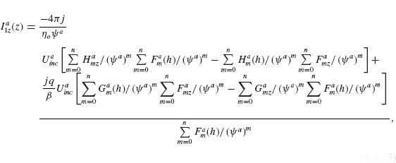
We then follow an iteration procedure as discussed in Reference 33 and use boundary condition (6.A.3) to eliminate C1 and solve the integral equation (6.A.22). The current distribution in the rod No.1 to the nth-order correction for the antisymmetric mode is
in which
(6.A.26) 
and
where X can be F, G, or H and  is the same as Ja(z) in Equation 6.A.24 but with
  substituted for
  According to Equation 6.A.25, the solution with the first-order correction is
(6.A.30) 
where
(6.A.31) 
and
(6.A.32) 
The zeroth-order current for normal incidence (q = 0) is
which is exactly the same as the zeroth-order solution of the current in an infinitely thin straight receiving antenna of length 2h [33]. This makes sense because in the zeroth-order approximation the electromagnetic interactions between different parts of a V-antenna are not considered. Therefore its optical response is only determined by the antenna length as shown in Equation 6.A.33.
We can similarly derive the integral equation for current in the first rod for the symmetric mode:
(6.A.34) 
where
(6.A.35) 
(6.A.36) 
(6.A.37) 
(6.A.38) 
in which  is the component of the incident electric field driving the symmetric mode (Fig. 6.A.1A).
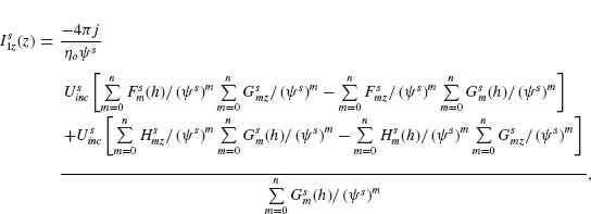
The current distribution in the rod No.1 to the nth-order correction for the symmetric mode is
where
(6.A.40) 
and F, G, and H are similarly defined as in Equations 6.A.27, 6.A.28, and 6.A.29.
The current distribution with the first-order correction is
(6.A.41) 
where
(6.A.42) 
and
(6.A.43) 
The zeroth-order current for normal incidence (q = 0) is
Let h = 2h' and z = z' + h' in Equation 6.A.44. We have
(6.A.45) 
Thus we recover the zeroth-order current distribution in an infinitely thin straight receiving antenna of length 2h' = h. One can further check that according to Equation 6.A.44,
(6.A.46) 
That is, there is no current at the joint of the V-antenna for the symmetric mode.
The above derivation assumes that the antenna is made of a perfect electric conductor. To model real metals, one has to add a term to the right-hand side of Equation 6.A.7 and the new boundary condition on the surface of the rod No. 1 reads
where zi is the surface impedance per unit length of the antenna [33]:
(6.A.48) 
The concept of surface impedance is valid for mid-infrared and longer wavelengths [37]. If the displacement current is much smaller than the conduction current as in the case of highly conductive metals  the impedance per unit length of antenna will be
(6.A.49) 
As a result of the correction in Equation 6.A.47, one additional term should be added to Equation 6.A.29 for the antisymmetric mode and the similar expression for the symmetric mode (other equations previously derived will not change):
(6.A.50) 
Combining the results of current distributions for the antisymmetric and symmetric modes, Equations 6.A.25 and 6.A.39, the currents in the two antenna arms can be written as
(6.A.51) 
(6.A.52) 
based on which one can calculate the amplitude and phase shift of antenna radiation in the far field. Corrections up to the second order were used in our calculations (Figs. 6.2d and 6.2e).
REFERENCES
1. Grober RD, Schoelkopf RJ, Prober DE (1997) Optical antenna: towards a unity efficiency near-field optical probe. Appl. Phys. Lett. 70: 1354–1356.
2. Novotny L, van Hulst N (2011) Antennas for light. Nat. Photon. 5: 83–90.
3. Xu Q, Bao J, Rioux RM, Perez-Castillejos R, Capasso F, Whitesides GM (2007) Fabrication of large-area patterned nanostructures for optical applications by nanoskiving. Nano Lett. 7: 2800–2805.
4. Sukharev M, Sung J, Spears KG, Seideman T (2007) Optical properties of metal nanoparticles with no center of inversion symmetry: observation of volume plasmons. Phys. Rev. B 76: 184302.
5. Biagioni P, Huang JS, Duò L, Finazzi M, Hecht B (2009) Cross resonant optical antenna. Phys. Rev. Lett. 102: 256801.
6. Ginn J, Shelton D, Krenz P, Lail B, Boreman G (2010) Polarized infrared emission using frequency selective surfaces. Opt. Express 18: 4557–4563.
7. Watanabe T, Fujii M, Watanabe Y, Toyama N, Iketaki Y (2004) Generation of a doughnut-shaped beam using a spiral phase plate. Rev. Sci. Instrum. 75: 5131.
8. McLeod JH (1954) The axicon—a new type of optical element. J. Opt. Soc. Am. 44: 8.
9. Casasent D (1977) Spatial light modulators. Proc. IEEE 65: 1.
10. Goodman JW (2004) Introduction to Fourier Optics. Roberts & Co.
11. Pendry JB, Schurig D, Smith DR (2006) Controlling electromagnetic fields. Science 312: 1780–1782.
12. Leonhardt U (2006) Optical conformal mapping. Science 312: 1777–1780.
13. Cai W, Shalaev V (2009) Optical Metamaterials: Fundamentals and Applications. Springer.
14. Engheta N, Ziolkowski RW (2006) Metamaterials: Physics and Engineering Explorations. Wiley-IEEE Press.
15. Yu N, Genevet P, Kats MA, Aieta F, Tetienne JP, Capasso F, Gaburro Z (2011) Light propagation with phase discontinuities: generalized laws of reflection and refraction. Science 334: 333–337.
16. Kats MA, Yu N, Genevet P, Gaburro Z, Capasso F (2011) Effect of radiation damping on the spectral response of plasmonic components. Opt. Express 19: 21749.
17. Kats MA, Genevet P, Aoust G, Yu N, Blanchard R, Aieta F, Gaburro Z, Capasso F. (2012) Giant birefringence in optical antenna arrays with widely tailorable optical anisotropy. Proceedings of the National Academy of Sciences of the United States of America 109: 12364–12368
18. Genevet P, Yu N, Aieta F, Lin J, Kats MA, Blanchard R, Scully MO, Gaburro Z, Federico Capasso (2012) Ultra-thin plasmonic optical vortex plate based on phase discontinuities. Appl. Phys. Lett. 100: 013101.
19. Aieta1 F, Genevet P, Yu N, Kats MA, Gaburro Z, Capasso F. Out-of-plane reflection and refraction of light by plasmonic interfaces with phase discontinuities. Submitted to Nat. Phys.
20. Blanchard R, Aoust G, Genevet P, Yu N, Kats MA, Gaburro Z, Capasso F (2012) Modelling nanoscale V-shaped antennas for the design of optical phased arrays. Phys. Rev. B 85: 155457.
21. Miyazaki HT, Kurokawa Y (2006) Controlled plasmon resonance in closed metal/insulator/metal nanocavities. Appl. Phys. Lett. 89: 211126.
22. Fattal D, Li J, Peng Z, Fiorentino M, Beausoleil RG (2010) Flat dielectric grating reflectors with focusing abilities. Nat. Photonics 4: 466–470.
23. Fan1 JA, Wu C, Bao K, Bao J, Bardhan R, Halas NJ, Manoharan VN, Nordlander P, Shvets G, Capasso F (2010) Self-assembled plasmonic nanoparticle clusters. Science 328: 1135–1138.
24. Luk'yanchuk B, Zheludev NI, Maier SA, Halas NJ, Nordlander P, Giessen H, Chong CT (2010) The Fano resonance in plasmonic nanostructures and metamaterials. Nat. Mater. 9: 707–715.
25. Hu X, Chan CT, Ho KM, Zi J (2011) Negative effective gravity in water waves by periodic resonator arrays. Phys. Rev. Lett. 106: 174501.
26. Liu Z, Zhang X, Mao Y, Zhu YY, Yang Z, Chan CT, Sheng P (2000) Locally resonant sonic materials. Science 289: 1734–1736.
27. Jackson JD (1999) Classical Electrodynamics. 3rd ed. John Wiley & Sons, Inc. p 665.
28. King RWP (1956) The Theory of Linear Antennas. Harvard University Press.
29. Maier SA (2007) Plasmonics: Fundamentals and Applications. Springer.
30. Novotny L, Bert H (2011) Principles of Nano-Optics. Cambridge University Press.
31. Zuloaga J, Nordlander P (2011) On the energy shift between near-field and far-field peak intensities in localized plasmon systems. Nano Lett. 11: 1280.
32. Zhang S, Genov DA, Wang Y, Liu M, Zhang X (2008) Plasmon-induced transparency in metamaterials. Phys. Rev. Lett. 101: 047401.
33. Liu N, Langguth L, Weiss T, Kastel J, Fleischhauer M, Pfau T, Giessen H (2009) Plasmonic analogue of electromagnetically induced transparency at the Drude damping limit. Nat. Mater. 8: 758.
34. Griffiths DJ (1999) Introduction to Electrodynamics. 3rd ed. Benjamin Cummings.
35. Heitler W (1954) The Quantum Theory of Radiation. 3rd ed. London: Oxford University Press.
36. Kelly KL, Coronado E, Zhao LL, Schatz GC (2003) The optical properties of metal nanoparticles: the influence of size, shape, and dielectric environment. J. Phys. Chem. B 106: 668.
37. Grady NK, Halas NJ, Nordlander P (2004) Influence of dielectric function properties on the optical response of plasmon resonant metallic nanoparticles. Chem. Phys. Lett. 399: 167.
38. Bruzzone S, Malvaldi M, Arrighini GP, Guidotti C (2004) Light scattering by gold nanoparticles: role of simple dielectric models. J. Phys. Chem. B 108: 10853.
39. Grimault AS, Vial A, de la Chapelle ML (2006) Modeling of regular gold nanostructures arrays for SERS applications using a 3D FDTD method. Appl. Opt. B 84: 111.
40. Bryant GW, de Abajo FJG, Aizpurua J (2008) Mapping the plasmon resonances of metallic nanoantennas. Nano Lett. 8: 2.
41. Ross BM, Lee LP (2009) Comparison of near- and far-field measures for plasmon resonance of metallic nanoparticles. Opt. Lett. 34: 7.
42. Palik ED (1997) Handbook of Optical Constants of Solids. Vol. 3. Academic Press.
43. Ashcroft NW, Mermin ND (1976) Solid State Physics. Thomson.
44. van Driel HM (1984) Optical effective mass of high density carriers in silicon. Appl. Phys. Lett. 44: 6.
45. Stutzman WL, Thiele GA (1981) Antenna Theory and Design. New York: John Wiley & Sons, Inc.
46. Balanis CA (1982) Antenna Theory, Analysis and Design. New York: John Wiley & Sons, Inc.
47. Orfanidis SJ. (2010) online publication Electromagnetic Waves and Antennas. http://www.ece.rutgers.edu/~orfanidi/ewa.
48. Engheta N, Papas CH, Elachi C (1982) Radiation patterns of interfacial dipole antennas. Radio Sci. 17: 1557.
49. Cubukcu E, Capasso F (2009) Optical nanorod antennas as dispersive one-dimensional Fabry-Perot resonators for surface plasmons. Appl. Phys. Lett. 95: 201101.
50. Huang J-S, Kern J, Geisler P, Weinmann P, Kamp M, Forchel A, Biagioni P, Hecht B (2010) Mode imaging and selection in strongly coupled nanoantennas. Nano Lett. 10: 2105–2110.
51. Brorson SD, Haus HA (1988) Diffraction gratings and geometrical optics. J. Opt. Soc. Am. B 5: 247–248.
52. Feynman RP, Hibbs AR (1965) Quantum Mechanics and Path Integrals. New York: McGraw-Hill.
53. Hecht E (1997) Optics. 3rd ed. Addison Wesley Publishing Company.
54. Veselago VG (1968) The electrodynamics of substances with simultaneously negative values of  and μ. Sov. Phys. Usp. 10: 509–514.
55. Pendry JB (2000) Negative refraction makes a perfect lens. Phys. Rev. Lett. 85: 3966–3969.
56. Shelby RA, Smith DR, Schultz S (2001) Experimental verification of a negative index of refraction. Science 292: 77–79.
57. Parazzoli CG, Greegor RB, Li K, Koltenbah BEC, Tanielian M (2003) Experimental verification and simulation of negative index of refraction using Snell's law. Phys. Rev. Lett. 90: 107401.
58. Houck AA, Brock JB, Chuang IL (2003) Experimental observations of a left-handed material that obeys Snell's law. Phys. Rev. Lett. 90: 137401.
59. Born M, Wolf E (1999) Principles of Optics. 7th ed. Cambridge University Press.
60. Ewald PP (1969) Introduction to the dynamical theory of X-ray diffraction. Acta Crystallogr. A 25: 103–108.
61. Kikuta H, Ohira Y, Iwata K (1997) Achromatic quarter-wave plates using the dispersion of form birefringence. Appl. Opt. 36: 7.
62. Sung J, Sukharev M, Hicks EM, Van Duyne RP, Seideman T, Spears KG (2008) Nanoparticle spectroscopy: birefringence in two-dimensional arrays of L-shaped silver nanoparticles. J. Phys. Chem. C 112: 3252.
63. Feng L, Mizrahi A, Zamek S, Liu Z, Lomakin V, Fainman Y (2011) Metamaterials for enhanced polarization conversion in plasmonic excitation. ACS Nano 5: 6.
64. Shcherbakov MR, Dobynde MI, Dolgova TV, Tsai D-P, Fedyanin AA (2010) Full Poincare sphere coverage with plasmonic nanoslit metamaterials at Fano resonance. Phys. Rev. B 82: 193402.
65. Nye JF, Berry MV (1974) Dislocations in wave trains. Proc. R. Soc. Lond. A 336: 165–190.
66. Padgett M, Courtial J, Allen L (2004) Light's orbital angular momentum. Phys. Today 57: 35–40.
67. Allen L, Beijersbergen MW, Spreeuw RJC, Woerdman JP (1992) Orbital angular momentum of light and the transformation of Laguerre-Gaussian laser modes. Phys. Rev. A 45: 8185–8189.
68. Beijersbergen MW, Coerwinkel RPC, Kristensen M, Woerdman JP (1994) Helical-wavefront laser beams produced with a spiral phaseplate. Opt. Commun. 112: 321–327.
69. Heckenberg NR, McDuff R, Smith CP, White AG (1992) Generation of optical phase singularities by computer-generated holograms. Opt. Lett. 17: 221–223.
70. Yu V, Vasnetsov MV, Soskin MS (1990) Laser beams with screw dislocations in their wavefronts. JETP Lett. 52: 429.
71. White AG, Smith CP, Heckenberg NR, Rubinsztein-Dunlop H, McDuff R, Weiss CO, Tamm C (1991) Interferometric measurements of phase singularities in the output of a visible laser. J. Mod. Opt. 38: 2531.
72. M., Berry, Nye J, Wright F (1979) The elliptic umbilic diffraction catastrophe. Philos. Trans. R. Soc. Lond. 291: 453.
73. Coullet P, Gil L, Rocca F (1989) Optical vortices. Opt. Commun. 73: 403.
74. Genevet P, Barland S, Giudici M, Tredicce JR (2010) Bistable and addressable localized vortices in semiconductor lasers. Phys. Rev. Lett. 104: 223902.
75. Hell SH (2007) Far-field optical nanoscopy. Science 316: 1153.
76. He H, Friese MEJ, Heckenberg NR, Rubinsztein-Dunlop H (1995) Direct observation of transfer of angular momentum to absorptive particles from a laser beam with a phase singularity. Phys. Rev. Lett. 75: 826–829.
77. Padgett M, Bowman R (2011) Tweezers with a twist. Nat. Photonics 5: 343.
78. Leach J, Padgett MJ, Barnett SM, Franke-Arnold S, Courtial J (2002) Measuring the orbital angular momentum of a single photon. Phys. Rev. Lett. 88: 257901.
79. Gibson G, Courtial J, Padgett M, Vasnetsov M, Pas'ko V, Barnett S, Franke-Arnold S (2004) Free-space information transfer using light beams carrying orbital angular momentum. Opt. Express 12: 5448–5456.
80. Siegman AE (1986) Lasers. Sausalito, CA: University Science Books. Chapter 16.


