8
Terahertz Plasmonic Surfaces for Sensing
The terahertz (THz) band occupies the region in the electromagnetic spectrum between microwaves and infrared, lying at the intersection of the electronic and optical regimes. It is broadly defined as the electromagnetic energy with wavelength range between 1000 and 100 μm (300 GHz and 3 THz). The band has attracted significant attention in recent years due to its scientific richness and promise of many exciting new applications which exploit the unique properties of this submillimeter-wave radiation. Potential applications span the gamut from the detection of chemical, biological, and explosive agents, security imaging and material science, to biomedical applications [1, 2].
The adaption of plasmonic concepts from the optical region of the spectrum to the THz band offers the exciting potential to realize new applications as well as overcome some of the limitations of the band. The inherently long wavelength of THz radiation poses a challenge for sensing and imaging objects of interest with feature sizes below the diffraction limit of hundreds of microns. The deep subwavelength confinement offered by plasmonics allows objects well below this limit to be sensed and imaged. Furthermore, the weakness of THz sources and the deficiency of its detectors can be somewhat compensated for by the use of resonant plasmonic structures to locally confine and enhance the electromagnetic field, allowing for sensitive detection.
This chapter first briefly examines some of the sensing applications of THz radiation that make the band so interesting. We then show how THz plasmonics can be realized by way of semiconductor and engineered metal surfaces and how they can be applied toward sensing. The use of THz plasmonic antennas for receiving and concentrating THz radiation and the phenomena of extraordinary transmission (ET) in the THz band are described in Sections 8.5 and 8.6, respectively. The chapter concludes with a description of some of the possibilities offered by the exciting new material graphene.
8.1 THE TERAHERTZ REGION FOR SENSING
THz radiation has a number of unique properties which make it suitable for a range of applications, which are often not possible elsewhere in the spectrum. It shares the ability of radio waves to penetrate a large range of nonmetallic, nonpolar substances such as cardboards, plastics, and common clothing fabrics but with a wavelength short enough to allow a submillimeter imaging resolution. X-rays have a similar ability to penetrate materials; however, the low energy of THz photons means that THz radiation does not pose the same ionizing risk to biological tissues.
Perhaps the most compelling feature of THz waves is the fact that a large number of atoms and molecules have rotational, translational, and vibrational responses which uniquely occur in the THz band [3]. Gases, in particular, have strong and narrow absorption lines. These responses allow substances to be distinguished and identified based on their THz spectral signature or fingerprint. Some examples of this include detecting biological agents [4, 5] and explosives [6–8] and chemical recognition of gas mixtures [9, 10]. While surface plasmon-based sensors are typically sensitive over a narrow frequency range, they can be designed to target specific narrowband spectral features, allowing a specific substance to be detected.
One area where THz surface plasmon sensors may play an important role is in the field of biosensing. THz radiation allows for the direct probing of the molecular dynamics of many biomolecules. For large biomolecules, the THz response is primarily determined by the low-frequency vibrational modes and side chain rotations [11, 12]. The high density of state of these modes means that individual absorption lines cannot be easily resolved leading to a broad THz absorption spectrum that is relatively featureless; however, this spectrum tends to be different between biomolecules allowing them to be distinguished [11–13].
THz waves have been shown to be highly sensitive to hydration, binding, and conformational change of proteins which may prove useful for sensing applications [12]. Nagel et al. demonstrated the label-free analysis of DNA molecules using THz radiation [14]. Combining surface plasmon sensors with microfluidic chips offers the most promising approach to realizing sensitive THz biochips [15, 16].
8.2 THz PLASMONICS
The metals commonly employed in the visible part of the spectrum for supporting SPPs, such as gold and silver, have significantly different properties in the THz regime which make them less suitable for sustaining SPPs at a flat interface. Far below their plasma frequency, these materials have significantly larger negative real and positive imaginary parts of the permittivity, more closely resembling a perfect electric conductor (PEC). Higher conductivity means that an SPP's electric field only slightly penetrates the metal causing it to be loosely bound to the surface and exhibit poor confinement, losing many of its advantages.
There are two common approaches for overcoming this lack of confinement. The first is to replace the metal with a semiconductor whose lower free-carrrier density causes its plasma frequency to fall in the THz band. This approach allows many plasmonic devices operating in the visible part of the spectrum to be simply scaled to operate in the THz band and has the additional advantage that the material dielectric properties can be tuned through optical, thermal, or electronic means, providing a way to actively control the SPPs propagation. The second approach is to use metals whose surface has been textured so that the electric field effectively penetrates further into the metal side of the interface. These engineered metal surfaces support SPP-like modes which are called designer or spoof surface plasmon polaritons (SSPPs) because their dispersion properties closely resemble real SPPs. The theory and properties of SPPs and SSPPs as well as their sensing applications will be discussed in Sections 8.3 and 8.4, respectively.
8.3 SPPs ON SEMICONDUCTOR SURFACES
The complex dielectric function of many semiconductors in the THz regime can be described by the Drude model, which we reprint here for convenience:
where  ∞ is the high-frequency permittivity and γ = e/m*μ is the characteristic collision frequency with μ being the carrier mobility. The plasma frequency is given by
  , where n is the free-carrier density, e the electron charge, m* the effective charge mass, and
  0 the permittivity of free space.
Since the plasma frequency is primarily determined by the free-carrier density, choosing an intrinsic or doped semiconductor with an appropriate carrier density allows the plasma frequency to be shifted to a desired frequency in the THz band. Ideally, the semiconductor should have a high carrier mobility to reduce the carrier collision frequency and hence loss due to absorption. Materials that suit these requirements include InSb, GaAs, and InAs. Another commonly used material is p- or n-doped silicon despite its comparatively lower carrier mobility.
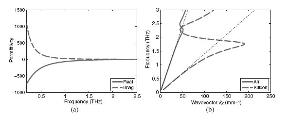
Intrinsic InSb has one of the highest carrier mobilities for a bulk semiconductor and is often the material of choice for THz plasmonics [17]. With a carrier density of n  1.6 × 1016 cm−3, it has a plasma frequency of ωp = 9.60 THz and collision frequency of γ = 1.79 THz [18]. Its permittivity properties are plotted in Figure 8.1a and the dispersion characteristics for an SPP propagating at air–InSb and silicon–InSb interfaces are shown in Figure 8.1b. It can be seen that a modest amount of confinement is possible when the frequency approaches the surface plasmon frequency, limited primarily by the loss in the InSb.
FIGURE 8.1 (a) Complex permittivity of InSb. (b) Dispersion properties of an SPP propagating on air–InSb and silicon–InSb interfaces.
Gómez-Rivas et al. [19] and Kuttge et al. [20] have demonstrated the propagation of SPPs on gratings made from n- and p-doped silicon wafers. The grating structuring of the surface was shown to provide additional degrees of freedom for tailoring the SPP propagation characteristics allowing the group velocity to be controlled as well as the creation of stop gaps in the spectral response. It was shown that resonant scattering at the edge of the stop gap reduced the group velocity by a factor of two which is useful for broadband spectroscopy and nonlinear applications [19].
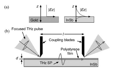
Isaac et al. demonstrated the much greater sensitivity offered by an SPP propagating on the surface of InSb compared to a planar gold surface in Reference 21. In their experimental configuration, depicted in Figure 8.2, they used razor blades as scatterers to couple free-space propagating THz waves to and from an SPP traveling on an InSb or gold surface. They showed that the enhanced confinement of the SPP on the InSb surface leads to a stronger light–matter interaction than for the gold case and was capable of sensing thin polymer layers which were a thousand times thinner than the THz free-space wavelength.
FIGURE 8.2 (a) Improved confinement of the electric field on an InSb surface compared with a gold surface. (b) Diagram of the experimental configuration showing how the THz energy is coupled into and out of the propagating SPP mode. Reprinted with permission from Reference 21. Copyright 2008 American Institute of Physics.
8.3.1 Active Control of Semiconductor Plasmonics
The nature of the electronic band structure of semiconductors allows the tuning of their material properties, which in turn creates the possibility of controlling the characteristics of SPPs excited on their surface. The existence of a band gap and unfilled electron energy states in the conduction band of semiconductors means that electrons can be promoted from the valence band to the conduction band, varying the free-carrier density which modifies the Drude dielectric response of the material. This can be achieved through photo-excitation of electrons or by varying the material’s temperature. Alternatively, an applied electric field can be used to create a local depletion region or free carriers can be directly injected to increase the local density.
Examining the Drude model given by Equation 8.1, it can be seen that the square of the plasma frequency is proportional to the free-carrier density. The collision frequency is also affected by an increase in free-carrier density through the accompanying reduction in carrier mobility. This means that as a semiconductor’s temperature is increased or is illuminated with light containing photons with energy greater than the semiconductor’s band gap, the material properties become more metallic-like with the skin depth and SPP confinement being reduced. Of all the methods for modifying the free-carrier density, photo-excitation holds the most promise since it offers the possibility of controlling plasmons on picosecond timescales [22], opening the door to ultrafast active plasmonic components in the THz range.
A significant amount of work on active THz plasmonics has focused on modifying the transmission properties of THz radiation through gratings of subwavelength apertures [17, 22–26]. The sensitivity of these structures to the dielectric properties of the underlying semiconductor makes them ideal for active control. The phenomena of ET will be discussed later in Section 8.6.
8.4 SSPP ON STRUCTURED METAL SURFACES
Surface waves propagating on metal–dielectric interfaces have been studied for more than a century, beginning with the seminal work of Sommerfeld investigating propagation on cylindrical surfaces (Sommerfeld waves) in 1899 [27] and Zenneck examining propagation on flat surfaces (Zenneck waves) in 1907 [28]. The surface waves studied were highly delocalized with the field extending a significant distance into the dielectric and closely resemble a plane wave propagating at a grazing angle to the surface. In 1950, Goubau [29] demonstrated that structuring the metal surface or the addition of a thin dielectric coating to the interface allowed the field extension to be controlled and confinement improved.
More recently, Pendry et al. [30] showed that a highly conductive metal surface perforated with subwavelength holes would support a surface wave and pointed out its connection with SPPs in the optical regime. As a result, these waves have since been termed spoof surface plasmon polaritons. The addition of the holes to the metal surface allows the field to effectively penetrate further into the metal, improving confinement of the wave. The use of general texturing of the metal surface allows us to engineer a Drude-like response similar to that of a metal close to the plasma frequency and gives us control over the propagation characteristics and plasmon confinement [30–32]. This ability to tailor the surface characteristics means that we can replicate the plasmon sensing undertaken in the visible part of the spectrum in the THz region while taking advantage of the unique properties of THz radiation. Some potential applications of SSPPs are subwavelength waveguiding [33–36], superfocusing [37, 38], near-field imaging, and biosensing with improved sensitivity.
A number of researchers have examined THz SSPPs propagating on corrugated or grooved surfaces [39, 40], hole arrays [40–44], and gratings [45]. More exotic spoof plasmon waveguides considered include wedges [33], V-channels [34], dominos [35], and slanted grooves [36]. As an illustrative example, we consider the relatively simple case of an SSPP propagating on a 1D grooved highly conductive metal surface. The dispersion relationship for this geometry can be derived by matching the field inside the grooves with the field above in vacuum. This is done by expanding the field inside the grooves in terms of the forward and backward propagating fundamental TE mode. The field above the surface is expressed in terms of an incident p-polarized free-space wave and its reflection from the surface. Matching the fields and applying the relevant boundary condition leads to the dispersion equation [32, 40]
(8.2) 
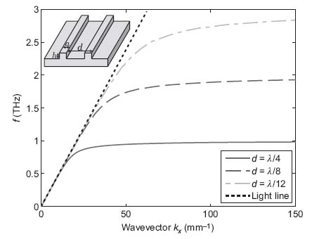
where k0 is the free-space wave vector, d the groove spacing, a the groove width, and h the groove height. Plotting this dispersion relationship in Figure 8.3 for the case a = 0.2d and h = d, we can see that despite the highly conductive nature of the metal, the wave vector kx bends away from the light line and strong confinement is achieved. It can be observed that by simply varying the parameters defining the geometry (d, a, and h) the surface wave properties can be controlled and this is demonstrated for several values of d in Figure 8.3.
FIGURE 8.3 Dispersion diagram for an SSPP propagating on a highly conductive grooved surface. The plot was generated using the parameters a = 0.2d and h = d, with several different groove spacings d as indicated in the plot legend as a fraction of the free-space wavelength λ at 1 THz.
We next consider the case of an SSPP propagating on the surface formed by a 2D array of holes in a highly conductive metal which are filled with a dielectric material of permittivity  . The holes are assumed to be square with dimension a × a and have an array period of d in both dimensions of the interface. Using a similar approach to the grooved surface case, we look for divergences in the reflection coefficient of the incident field due to coupling to a surface mode. From this the dispersion relationship can then be shown to be [40]
(8.3) 
where
(8.4) 
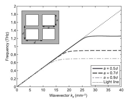
Figure 8.4 plots this dispersion characteristic when d = 75 μm for the three cases: a = 0.5d, a = 0.7d, and a = 0.9d. It can be again seen that by structuring the surface, in this case with appropriately sized and spaced holes, the dispersion relationship can be engineered to achieve a tight confinement at any desired frequency in the THz band.
FIGURE 8.4 Dispersion diagram for an SSPP propagating on the surface of a 2D square hole array in a highly conductive metal filled with a dielectric of permittivity  = 10. The hole period is d = 75 μm with several different hole dimensions a × a as indicated in the plot legend.
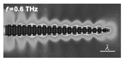
Metal wires can also be used to efficiently guide THz radiation [37, 46–50]. Maier et al. demonstrated how surface corrugations on wires can be exploited to confine and focus an SSPP to make a THz probe in Reference 37. Figure 8.5 illustrates how the surface geometry of the corrugated wire was used to greatly reduce the radial extent of the SSPP electric field and achieve subwavelength concentration of the energy at the tip. This probe could be used as a flexible endoscope for spectroscopy or imaging well below the diffraction limit [48].
FIGURE 8.5 Focusing and guiding of an SSPP on a corrugated PEC cone surface. Reprinted with permission from Reference 49. Copyright 2008 IEEE.
8.5 THz PLASMONIC ANTENNAS
Antennas provide an efficient means of transferring freely propagating electromagnetic waves from the far field to the near field, wherein the energy can be localized and concentrated into a subwavelength volume. The advantage of using an antenna is that it allows the diffraction limit to be overcome and the field intensity to be enhanced by several orders of magnitude at a defined location. It is for these reasons that optical nanoantennas have been found useful for a range of applications [51, 52] and it is therefore useful to extend the concept to the THz region. Sensing applications of THz antennas will likely be found in technological areas such as spectroscopy, biosensing, and security.
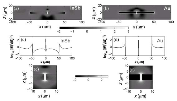
It is possible to adapt conventional (typically metal-based) antenna designs commonly used in the radiowave and microwave regimes for use in the THz band since metals remain reasonably conductive. However, it has been shown by Giannini et al. [53] that the adoption of plasmonic antennas allows greater enhancement of THz radiation. For example, in Figure 8.6 the field enhancement of a rectangular dimer antenna made from gold is compared with one made from InSb. It can be seen that the localized plasmonic resonance in the InSb antenna achieves a field enhancement of the order of 102–103 in the gap between dimers, which is greater than that for the gold antenna. Bow-tie antennas which are formed from two triangular dimers with their apex facing each other and a subwavelength gap in-between have been demonstrated to have even higher field enhancement than rectangular dimer antennas, partly due to the lightning rod effect which occurs at the triangle corners [53, 54].
FIGURE 8.6 (a) Near-field intensity distribution at the resonance of an InSb dimer antenna with a gap Δ = 2 μm, length L = 50 μm, height h = 5 μm, and f = 1.62 THz. (b) Gold antenna with the same dimension as (a) but at f = 1.73 THz. (c) Horizontal cut of (a) at z = 0. (d) Horizontal cut of (b) at z = 0. (e) Close-up view of the gap of (a). (f) Close-up view of the gap of (b). Reprinted with permission from Reference 53. Copyright 2010 Optical Society of America.
Plasmonic antennas that have a broadband response can be designed through the use of transformation optics, which has been demonstrated as a technique for transferring the broad bandwidth behavior of plasmonic waveguides to nano- and micro-antennas using geometric singularities [55]. A broad bandwidth response is important for sensing applications where the object being sensed has a broad dielectric response such as in the case of large biomolecules rather than a narrowband resonance.
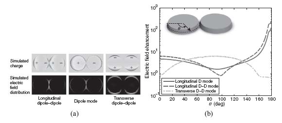
Hanham et al. [18] investigated a periodic array of THz InSb disk dimers which were only just touching, a geometry shown in Figure 8.7 which has been predicted by transformation optics to efficiently harvest light over a broad bandwidth [55]. He demonstrated that the plasmonic interaction between the disks led to spectral broadening of the absorption cross section of the structure due to the excitation of multiple plasmonic modes. When an incident wave’s polarization aligns with the dimer axis then single dipole and double dipole longitudinal modes are excited on the structure. Their charge distribution shown in Figure 8.8a reveals the associated buildup of charge in the disk gap region which leads to a strong field enhancement in the gap. In contrast, the transverse dipole mode which is excited when illuminated with orthogonally polarized light does not display the same field enhancement, underlining the importance of the plasmonic interaction between the disks for field enhancement. Figure 8.8b plots the field enhancement seen around the outside of the disk dimers relative to the incoming wave amplitude for several modes supported by the touching disks structure. It can be seen that the field is enhanced by a factor of 270 in the sub-micron gap between the disks.
FIGURE 8.7 THz InSb touching disks. (a) The periodic array of disk dimers. (b) A close-up view of the touching region of one of the dimers. Reprinted with permission from Reference 18. Copyright 2012 WILEY-VCH Verlag GmbH & Co. KGaA, Weinheim.
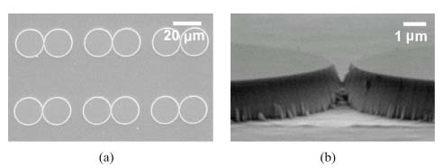
FIGURE 8.8 (a) Charge and electric field distribution for the modes supported by the touching disk dimers. (b) Simulated electric field amplitude enhancement for the different modes. Reprinted with permission from Reference 18. Copyright 2012 WILEY-VCH Verlag GmbH & Co. KGaA, Weinheim.
An important property of semiconductor-based THz antennas is their ability to be controlled and tuned. As discussed in Section 8.3.1, a semiconductor’s dielectric properties depend on free-carrier concentration and mobility. By modifying the free-carrier concentration, the far-field and near-field properties of an antenna can be controlled. A potential use of this could be modifying the resonant frequency of an antenna to scan in frequency for a spectroscopy-type application. Berrier et al. demonstrated this capability in Reference 54 where the resonant frequency of a bow-tie antenna was blue-shifted and its extinction spectra increased by 40% by increasing the illumination fluence of the silicon antenna by a frequency-doubled 800 nm pulsed laser.
Berrier et al. later demonstrated the use of doped silicon bow-tie antennas for enhanced sensing of thin dielectric layers [56]. By exciting LSPR modes on individual antennas and monitoring the resonant frequency shift due to the presence of an inorganic film they were able to detect films 3750 times thinner than the free-space wavelength. This is a 10 times improvement in sensitivity compared to the approach using an SPP propagating on a flat plasmonic surface [21, 56]. This technique is ideally suited for applications involving small sensing volumes such as cells, microorganisms, and explosives detection.
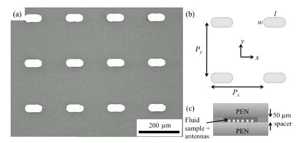
An interesting approach to sensing is the use of the collective response of an antenna array. In Reference 57, a 2D array of gold rectangular antennas are printed on a μm thick polyethylene naphthalate substrate, shown in Figure 8.9. The array is designed such that a diffractive mode of a normal incident THz wave couples to the individual dipole resonances of each antenna, creating a combined or lattice resonance of the array. This resonance can be used for sensing since the addition of a thin dielectric layer will modify the phase-matching condition required for the coupling between antennas resulting in a frequency shift of the resonance, which corresponds to a minimum in the extinction spectra of the array. This approach was shown to be useful for sensing thin films of liquids and gases and has a relatively high Q-factor of 20.
FIGURE 8.9 (a) Microscope image of the rectangular antenna array. (b) Schematic diagram of THz antenna array with antennas of length l = 85 μm, width w = 38 μm, and periods Px = 200 μm, and Py = 220 μm in the x and y directions, respectively. (c) Schematic diagram of the fluid chamber assembly used for transmission measurements. Reprinted with permission from Reference 57. Copyright 2011 Optical Society of America.
8.6 EXTRAORDINARY TRANSMISSION
The concept of extraordinary transmission (ET) where light incident on an aperture has a transmission efficiency greater than unity when normalized by the aperture area can be extended to the THz regime. This phenomenon has been explained by the tunneling of surface plasmons propagating on one or both sides of the surface containing the aperture [58–60]. For the case of an array of apertures, the scattering of the incident light on the aperture boundaries can lead to enhanced resonant excitation of surface plasmons which couple with neighboring apertures [61]. The excited SPP waves excite the waveguide mode inside each aperture which mediates the tunneling of light from the entrant to the exit surface. The size and geometry of the apertures determines whether the waveguide mode is evanescent or propagating and the strength of the coupling.
In the THz regime, semiconductor surfaces supporting SPPs have been shown to be suitable for achieving ET [17, 21, 23, 25, 26, 62]. These surfaces have the additional feature that the transmission properties can be controlled by modifying the temperature [26] or through above-bandgap photo-illumination [23, 25]. The latter has the advantage that the transmission properties can be rapidly varied allowing the creation of a THz switch or modulator with a broad bandwidth [23].
ET can also be achieved by way of spoof plasmons propagating on textured metal surfaces [63–66]. In this case, the requisite texturing of the metal surface to support the SSPP can be provided by the array of apertures in the surface. The periodicity of the apertures helps convert the normal incident light into SSPPs by providing the additional momentum required for their excitation [58]. The excited SSPPs propagate along the surface and couple to neighboring apertures aiding the excitation of the aperture waveguide mode.
The resonant nature of ET makes it extremely sensitive to the local dielectric environment near the apertures, which is ideal for the detection of small quantities of samples located in the vicinity. Miyamaru et al. have demonstrated the use of metal hole arrays for sensing thin dielectric films [66, 67]. By monitoring the frequency shift of the peak in transmission through the hole array, they were able to detect a 5 μm thick dielectric layer. They explained that the relatively long localization of the SSPP in the vicinity of the apertures leads to improved sensitivity over conventional THz spectroscopy approaches [67].
An interesting demonstration of the near-field imaging capabilities of a metal hole array is shown in Figure 8.10. Miyamaru et al. [65] acquired a THz image of a fingerprint deposited on a dielectric film using a metal plate containing a triangular lattice of holes and compared it with an image taken the conventional way. The metal hole array was placed in contact with the dielectric film to take advantage of the enhanced field strength around the holes and the subwavelength spatial sensitivity. The significantly improved resolution and sensitivity can be clearly seen in the images obtained.
FIGURE 8.10 (a) Photograph of a fingerprint deposited on a polypropylene film. THz image of the fingerprint created (b) with and (c) without the metal hole array. Reprinted with permission from Reference 65. Copyright 2007 Optical Society of America.

Other applications of aperture arrays include the creation of THz filters for probing specific frequency windows for possible spectral features, which may prove useful for applications in chemistry and biology. The advantage of using a hole array is that the transmitted frequency can be varied simply by adjusting the array period.
Seo et al. [68] showed that THz radiation could pass through a nano-slit in a metal plate with a gap width of only 70 nm, which is below the metal’s skin depth. The transmission of the THz radiation was accompanied by a two orders of magnitude increase in the electric field intensity inside the gap. It is thought that this approach could find application in near-field imaging and allow focusing of THz waves beyond the skin depth toward the Thomas–Fermi length scale.
8.7 THz PLASMONS ON GRAPHENE
Graphene is a promising material for the development of high-speed electronic devices due to its unique electronic structure which leads to useful phenomena such as massless charge carriers and ballistic transport [69, 70]. Graphene has several characteristics which make it extremely attractive for THz plasmonics. First, graphene will support THz plasmons when it is appropriately structured and the coupling of the plasmons to THz radiation is relatively strong despite the graphene surface being only a single atomic layer thick [71]. Second, the carrier concentration can be readily controlled through chemical doping and electrostatic gating [72]. This capability allows the plasmonic properties to be dynamically controlled and tailored across a single graphene sheet.
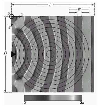
Engheta and coworkers demonstrated the extreme flexibility of graphene as a plasmonic material operating above the THz band in the mid-infrared in Reference 72. They were able to show theoretically how plasmonic devices such as waveguides and Luneburg lenses could be created by spatially manipulating the conductivity across the graphene surface. Figure 8.11 shows a simulation of their graphene Luneburg lens collimating a point source-excited SPP. By appropriately biasing the graphene they were able to grade the lenses’ conductivity such that a diverging plasmonic surface wave is refracted to form a collimated beam. Ju et al. showed along similar lines that microribbons of graphene can be used to create tuneable THz metamaterials [71]. This ability to engineer and control the properties of graphene combined with the extreme surface plasmon confinement makes graphene an ideal material for future THz plasmonic devices for sensing.
FIGURE 8.11 The collimation of an SPP by a Luneburg lens made from graphene. The plot shows the phase of the y-component of the electric field at f = 30 THz. In the plot D = 1.5 mm, w = 75 nm, L = 1.6 mm. Reprinted from Reference 72 with permission from AAAS.
REFERENCES
1. Siegel PH (2002) Terahertz technology. IEEE Trans. Microw. Theory Tech. 50(3): 910–928.
2. Siegel PH (2004) Terahertz technology in biology and medicine. IEEE Trans. Microw. Theory Tech. 52(10): 2438–2447.
3. Mittleman DM, Jacobsen RH, Nuss MC (1996) T-ray imaging. IEEE J. Sel. Top. Quant. 2(3): 679–692.
4. Brown ER, Woolard DL, Samuels AC, Globus T, Gelmont B (2002) Remote detection of bioparticles in the THz region. IEEE MTT-S Digest. Vol. 3. pp 1591–1594.
5. Wang S, Ferguson B, Abbott D, Zhang XC (2003) T-ray imaging and tomography. J. Biol. Phys. 29(2): 247–256.
6. Tribe WR, Newnham DA, Taday PF, Kemp MC (2004) Hidden object detection: security applications of terahertz technology. Proc. SPIE 5354: 168-176.
7. Huang F, Schulkin B, Altan H, Federici JF, Gary D, Barat R, Zimdars D, Chen M, Tanner DB (2004) Terahertz study of 1, 3, 5-trinitro-s-triazine by time-domain and Fourier transform infrared spectroscopy. Appl. Phys. Lett. 85(23): 5535–5537.
8. Federici JF, Schulkin B, Huang F, Gary D, Barat R, Oliveira F, Zimdars D (2005) THz imaging and sensing for security applications–explosives, weapons and drugs. Semicond. Sci. Technol. 20: S266-S280.
9. Jacobsen RH, Mittleman DM, Nuss MC (1996) Chemical recognition of gases and gas mixtures with terahertz waves. Opt. Lett. 21(24): 2011–2013.
10. Hassani A, Skorobogatiy M (2008) Surface plasmon resonance-like integrated sensor at terahertz frequencies for gaseous analytes. Opt. Express 16(25): 20206–20214.
11. Smye SW, Chamberlain JM, Fitzgerald AJ, Berry E (2001) Topical review: the interaction between terahertz radiation and biological tissue. Phys. Med. Biol. 46: R101–R112.
12. Markelz AG (2008) Terahertz dielectric sensitivity to biomolecular structure and function. IEEE J. Sel. Top. Quant. 14(1): 180–190.
13. Globus T, Woolard D, Bykhovskaia M, Gelmont B, Werbos L, Samuels A (2003) THz-frequency spectroscopic sensing of DNA and related biological materials. Int. J. High Speed Electron. Syst. 13(4): 903–936.
14. Nagel M, Richter F, Haring-Bolivar P, Kurz H (2003) A functionalized THz sensor for marker-free DNA analysis. Phys. Med. Biol. 48: 3625-3636.
15. Laurette S, Treizebre A, Bocquet B (2011) Co-integrated microfluidic and THz functions for biochip devices. J. Micromech. Microeng. 21: 065029.
16. George PA, Hui W, Rana F, Hawkins BG, Smith AE, Kirby BJ (2008) Microfluidic devices for terahertz spectroscopy of biomolecules. Opt. Express 16(3): 1577–1582.
17. Gómez-Rivas J, Janke C, Bolivar P, Kurz H (2005) Transmission of THz radiation through InSb gratings of subwavelength apertures. Opt. Express 13(3): 847–859.
18. Hanham SM, Fernández-Domínguez AI, Teng JH, Ang SS, Lim KP, Yoon SF, Ngo CY, Klein N, Pendry JB, Maier SA (2012) Broadband terahertz plasmonic response of touching InSb disks. Adv. Mater. 24(35): OP226–OP230.
19. Gómez-Rivas J, Kuttge M, Bolivar PH, Kurz H, Sánchez-Gil JA (2004) Propagation of surface plasmon polaritons on semiconductor gratings. Phys. Rev. Lett. 93(25): 256804.
20. Kuttge M, Kurz H, Rivas JG, Sánchez-Gil JA, Bolivar PH (2007) Analysis of the propagation of terahertz surface plasmon polaritons on semiconductor groove gratings. J. Appl. Phys. 101(2): 023707.
21. Isaac TH, Barnes WL, Hendry E (2008) Determining the terahertz optical properties of subwavelength films using semiconductor surface plasmons. Appl. Phys. Lett. 93(24): 241115–241115.
22. Gómez-Rivas J, Kuttge M, Kurz H, Bolivar PH, Sánchez-Gil JA (2006) Low-frequency active surface plasmon optics on semiconductors. Appl. Phys. Lett. 88(8): 082106.
23. Janke C, Rivas JG, Bolivar PH, Kurz H (2005) All-optical switching of the transmission of electromagnetic radiation through subwavelength apertures. Opt. Lett. 30(18): 2357–2359.
24. Hendry E, Lockyear MJ, Rivas JG, Kuipers L, Bonn M (2007) Ultrafast optical switching of the THz transmission through metallic subwavelength hole arrays. Phys. Rev. B 75(23): 235305.
25. Hendry E, García-Vidal FJ, Martín-Moreno L, Rivas JG, Bonn M, Hibbins AP, Lockyear MJ (2008) Optical control over surface-plasmon-polariton-assisted THz transmission through a slit aperture. Phys. Rev. Lett. 100(12): 123901.
26. Gómez-Rivas J, Bolivar PH, Kurz H (2004) Thermal switching of the enhanced transmission of terahertz radiation through subwavelength apertures. Opt. Lett. 29(14): 1680–1682.
27. Sommerfeld A (1899) Ueber die fortpanzung elektrodynamischer wellen längs eines drahtes. Ann. Phys-Berlin 303(2): 233–290.
28. Zenneck J (1907) Über die fortpanzung ebener elektromagnetischer wellen längs einer ebenen leiterfläche und ihre beziehung zur drahtlosen telegraphie. Ann. Phys-Berlin 328(10): 846–866.
29. Goubau G (1950) Surface waves and their application to transmission lines. J. Appl. Phys. 21(11): 1119–1128.
30. Pendry JB, Martín-Moreno L, García-Vidal FJ (2004) Mimicking surface plasmons with structured surfaces. Science 305(5685): 847–848.
31. Raether H (1988) Surface Plasmons on Smooth and Rough Surfaces and on Gratings. Vol. 111. Berlin: Springer.
32. Fernández-Domínguez AI, Martín-Moreno L, García-Vidal FJ (2011) In: Surface Electromagnetic Waves on Structured Perfectly Conducting Surfaces. Maradudin AA, editor. Structured Surfaces as Optical Metamaterials. Cambridge University Press. Chapter 7.
33. Fernández-Domínguez AI, Moreno E, Martín-Moreno L, García-Vidal FJ (2009) Terahertz wedge plasmon polaritons. Opt. Lett. 34(13): 2063–2065.
34. Fernández-Domínguez AI, Moreno E, Martín-Moreno L, García-Vidal FJ (2009) Guiding terahertz waves along subwavelength channels. Phys. Rev. B 79(23): 233104.
35. Martín-Cano D, Nesterov ML, Fernández-Domínguez AI, García-Vidal FJ, Martín-Moreno L, Moreno E (2010) Domino plasmons for subwavelength terahertz circuitry. Opt. Express 18(2): 754–764.
36. Wood JJ, Tomlinson LA, Hess O, Maier SA, Fernández-Domínguez AI (2012) Spoof plasmon polaritons in slanted geometries. Phys. Rev. B 85(7): 075441.
37. Maier SA, Andrews SR, Martín-Moreno L, García-Vidal FJ (2006) Terahertz surface plasmon-polariton propagation and focusing on periodically corrugated metal wires. Phys. Rev. Lett. 97(17): 176805.
38. Zhan H, Mendis R, Mittleman DM (2010) Superfocusing terahertz waves below λ/250 using plasmonic parallel-plate waveguides. Opt. Express 18(9): 9643–9650.
39. Mukina LS, Nazarov MM, Shkurinov AP (2006) Propagation of THz plasmon pulse on corrugated and at metal surface. Surf. Sci. 600(20): 4771–4776.
40. García-Vidal FJ, Martín-Moreno L, Pendry JB (2005) Surfaces with holes in them: new plasmonic metamaterials. J. Opt. A Pure Appl. Opt. 7: S97–S101.
41. Ulrich R, Tacke M (1973) Submillimeter waveguiding on periodic metal structure. Appl. Phys. Lett. 22(5): 251–253.
42. Williams CR, Andrews SR, Maier SA, Fernández-Domínguez AI, Martín-Moreno L, García-Vidal FJ (2008) Highly confined guiding of terahertz surface plasmon polaritons on structured metal surfaces. Nat. Photonics 2(3): 175–179.
43. Williams C, Misra M, Andrews S, Maier S, Carretero-Palacios S, Rodrigo S, García-Vidal F, Martín-Moreno L (2010) Dual band terahertz waveguiding on a planar metal surface patterned with annular holes. Appl. Phys. Lett. 96: 011101.
44. Maier SA, Andrews SR (2006) Terahertz pulse propagation using plasmon-polariton-like surface modes on structured conductive surfaces. Appl. Phys. Lett. 88(25): 251120.
45. Mills DL, Maradudin AA (1989) Surface corrugation and surface-polariton binding in the infrared frequency range. Phys. Rev. B 39(3): 1569.
46. King M, Wiltse J (1962) Surface-wave propagation on coated or uncoated metal wires at millimeter wavelengths. IRE Trans. Ant. Prop. 10(3): 246–254.
47. Wächter M, Nagel M, Kurz H (2005) Frequency-dependent characterization of THz Sommerfeld wave propagation on single-wires. Opt. Express 13(26): 10815–10822.
48. Wang K, Mittleman DM (2004) Metal wires for terahertz wave guiding. Nature 432(7015): 376–379.
49. Fernández-Domínguez AI, Martín-Moreno L, García-Vidal FJ, Andrews SR, Maier SA (2008) Spoof surface plasmon polariton modes propagating along periodically corrugated wires. IEEE J. Sel. Top. Quant. 14(6): 1515–152.
50. Fernández-Domínguez AI, Williams CR, García-Vidal FJ, Martín-Moreno L, Andrews SR, Maier SA (2008) Terahertz surface plasmon polaritons on a helically grooved wire. Appl. Phys. Lett. 93(14): 141109.
51. Giannini V, Fernández-Domínguez AI, Heck SC, Maier SA (2011) Plasmonic nanoantennas: fundamentals and their use in controlling the radiative properties of nanoemitters. Chem. Rev. 111: 3888–3912.
52. Novotny L, van Hulst N (2011) Antennas for light. Nat. Photonics 5(2): 83–90.
53. Giannini V, Berrier A, Maier SA, Sánchez-Gil JA, Rivas JG (2010) Scattering efficiency and near field enhancement of active semiconductor plasmonic antennas at terahertz frequencies. Opt. Express 18(3): 2797–2807.
54. Berrier A, Ulbricht R, Bonn M, Rivas JG (2010) Ultrafast active control of localized surface plasmon resonances in silicon bowtie antennas. Opt. Express 18(22): 23226–23235.
55. Aubry A, Lei DY, Fernández-Domínguez AI, Sonnefraud Y, Maier SA, Pendry JB (2010) Plasmonic light-harvesting devices over the whole visible spectrum. Nano Lett. 10(7): 2574–2579.
56. Berrier A, Albella P, Poyli MA, Ulbricht R, Bonn M, Aizpurua J, Gómez-Rivas J (2012) Detection of deep-subwavelength dielectric layers at terahertz frequencies using semiconductor plasmonic resonators. Opt. Express 20(5): 5052–5060.
57. Ng B, Hanham SM, Giannini V, Chen ZC, Tang M, Liew YF, Klein N, Hong MH, Maier SA (2011) Lattice resonances in antenna arrays for liquid sensing in the terahertz regime. Opt. Express 19(15): 14653–14661.
58. Ebbesen TW, Lezec HJ, Ghaemi HF, Thio T, Wolff PA (1998) Extraordinary optical transmission through sub-wavelength hole arrays. Nature 391(6668): 667–669.
59. Martín-Moreno L, García-Vidal FJ, Lezec HJ, Pellerin KM, Thio T, Pendry JB, Ebbesen TW (2001) Theory of extraordinary optical transmission through subwavelength hole arrays. Phys. Rev. Lett. 86(6): 1114–1117.
60. Genet C, Ebbesen TW (2007) Light in tiny holes. Nature 445(7123): 39–46.
61. Popov E, Bonod N (2011) Physics of extraordinary transmission through hole arrays. In: Maradudin AA, editor. Structured Surfaces as Optical Metamaterials. Cambridge University Press. Chapter 1.
62. Gómez-Rivas J, Schotsch C, Bolivar PH, Kurz H (2003) Enhanced transmission of THz radiation through subwavelength holes. Phys. Rev. B 68(20): 201306.
63. Qu D, Grischkowsky D, Zhang W (2004) Terahertz transmission properties of thin, subwavelength metallic hole arrays. Opt. Lett. 29(8): 896–898.
64. Cao H, Nahata A (2004) Resonantly enhanced transmission of terahertz radiation through a periodic array of subwavelength apertures. Opt. Express 12(6): 1004–1010.
65. Miyamaru F, Takeda MW, Suzuki T, Otani C (2007) Highly sensitive surface plasmon terahertz imaging with planar plasmonic crystals. Opt. Express 15(22): 14804–14809.
66. Miyamaru F, Sasagawa Y, Takeda MW (2010) Effect of dielectric thin films on reflection properties of metal hole arrays. Appl. Phys. Lett. 96(2): 021106.
67. Miyamaru F, Hayashi S, Otani C, Kawase K, Ogawa Y, Yoshida H, Kato E (2006) Terahertz surface-wave resonant sensor with a metal hole array. Opt. Lett. 31(8): 1118–1120.
68. Seo MA, Park HR, Koo SM, Park DJ, Kang JH, Suwal OK, Choi SS, Planken PCM, Park GS, Park NK, Park HQ, Kim SD (2009) Terahertz field enhancement by a metallic nano slit operating beyond the skin-depth limit. Nat. Photonics 3(3): 152–156.
69. Novoselov KS, Geim AK, Morozov SV, Jiang D, Katsnelson MI, Grigorieva IV, Dubonos SV, Firsov AA (2005) Two-dimensional gas of massless Dirac fermions in graphene. Nature 438(7065): 197–200.
70. Castro Neto AH, Guinea F, Peres NMR, Novoselov KS, Geim AK (2007) The electronic properties of graphene. Rev. Mod. Phys. 81(1): 109–162.
71. Ju L, Geng B, Horng J, Girit C, Martin M, Hao Z, Bechtel HA, Liang X, Zettl A, Shen YR, Wang F (2011) Graphene plasmonics for tuneable terahertz metamaterials. Nat. Nanotechnol. 6(10): 630–634.
72. Vakil A, Engheta N (2011) Transformation optics using graphene. Science 332(6035): 1291.
