9
Subwavelength Imaging by Extremely Anisotropic Media
9.1 INTRODUCTION TO CANALIZATION REGIME OF SUBWAVELENGTH IMAGING
Lens-based imaging devices such as conventional microscopes cannot provide resolution better than λ/2, where λ is the wavelength of radiation. This restriction is known as the diffraction limit, and holds irrespectively of the frequency of operation—from microwave frequencies up to the visible range. Conventional lenses operate only with the far field of the source, which is formed by propagating spatial harmonics. The information related to the near field of the source is transported by evanescent spatial harmonics, which exhibit exponential decay in all natural materials as well as in free space. For this reason, the subwavelength details of the near field are not directly accessible with conventional imaging systems. In practice, the near field can be scanned, point by point, using small near-field probes. However, scanning near-field microscopy is a rather slow process, and thus lenses that may enable the simultaneous imaging of the whole region of interest with super-resolution would be extremely useful.
The diffraction limit can be surpassed only if one adopts a conceptually different imaging technique. In order to obtain imaging with subwavelength resolution, it may be necessary to overstep beyond the frontiers of naturally available materials and to use specially engineered artificial media with electromagnetic properties not readily available in nature. In recent years, several techniques have been put forward aiming at imaging with super-resolution in different ranges of the electromagnetic spectrum. These proposals include perfect lenses [1], silver superlenses [2], hyperlenses [3–7], and stimulated emission depletion (STED) fluorescence microscopes [8]. Another option, which is the topic of this chapter, is based on the use of materials with extreme optical anisotropy.
Let us consider an uniaxial dielectric medium with permittivity dyadic of the form
(9.1) 
The dispersion equation for extraordinary waves in such medium reads
where kx, ky, kz are the components of wave vector k; ω is the frequency of operation; and c is the speed of light in vacuum.
If the material is characterized by extreme optical anisotropy such that  then Equation 9.2 has the following solution:
(9.3) 
Therefore, all extraordinary waves in a medium with extreme optical anisotropy are dispersionless: The electromagnetic waves travel along the optical axis of the material with a fixed phase velocity independently of the transverse phase variations. Note that  xx does not have to be necessarily a real number. It may be a complex number with a large absolute value. The imaginary part of
  xx representing losses has very little influence on the wave propagation.
To a good approximation, the class of dielectrics with extreme optical anisotropy can be described by a dielectric function of the form
The infinite value appearing in Equation 9.4 should not be treated as something exceptional or unusual. The corresponding material relations read as Ex = 0, Dy =  Ey, and Dz =
  Ez. This actually means that the medium is perfectly conducting along the x-direction.
The latter fact gives a hint of how media with extreme optical anisotropy can be created artificially. An array of parallel metallic wires, also known as “wire medium” [9], may provide the necessary properties at frequencies up to the infrared band [10] (see Sections 9.2, 9.3, and 9.4 for more details). In the visible range, one of the options may be a layered metal–dielectric structure [11] which has an effective permittivity consistent with Equation 9.4 (see Section 9.6 for more details).
Materials with extreme anisotropy have remarkable properties: All the extraordinary waves supported by the media are propagating waves (see Fig. 9.1). Thus, theoretically, it is possible to transport an arbitrary field distribution with suitable polarization through such material with no loss of resolution. Lenses formed by slabs of such materials provide a unique opportunity to transmit the near field with super-resolution. At the front interface with free space, the evanescent waves are transformed into propagating waves, which prevents their decay and preserves the subwavelength information. The propagating waves travel through the slab and reproduce the image at the back interface of the lens. This phenomenon is known as canalization [2]. This regime is especially appropriate for the transmission of images with super-resolution over significant distances in terms of the wavelength. This effect cannot be achieved using other available imaging techniques.
Basically, the canalization regime is very similar to the fiber-optic effect which is observed in the “TV rock” (see Fig. 9.2). This mineral consists of parallel tiny optical fibers which are capable of transporting images pixel by pixel. The significant difference is that the canalization regime provides super-resolution, whereas the resolution provided by the TV rock is determined by dimensions of the fibers which are greater than the wavelength. In order to get super-resolution one has to use an array of subwavelength waveguides such as an array of metallic wires.
An alternative and widely known opportunity of subwavelength imaging is the perfect lens concept [1]. It is based on the amplification of evanescent harmonics by a metamaterial, rather than on their conversion into propagating waves. This may enable imaging objects which are placed at some significant distance from the lens interface, like buried objects. However, the perfect lens relies on the resonant excitation of surface plasmon polaritons at the interfaces of a metamaterial slab, and hence it is very sensitive to losses [13]. The amplification of the evanescent waves requires such a low level of losses in the metamaterial that it may be extremely difficult to achieve in practice. Even if the current race to create the metamaterial required for the implementation of the perfect lens in the optical range [14–17] is successfully accomplished then such material will be inevitably lossy and its use as a subwavelength imaging device may be of limited interest.
The effect of losses on the canalization regime is much less restrictive. Losses cause the decay of propagating waves inside of the material, but the decaying factor is the same for the whole spatial spectrum. This means that losses cause only a degradation of intensity but do not corrupt the form of the image [18]. This makes lenses operating in the canalization regime easier to fabricate as compared to perfect lenses, regardless of the frequency range of operation.
9.2 WIRE MEDIUM LENS AT THE MICROWAVE FREQUENCIES
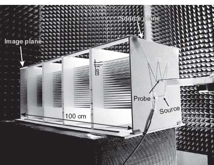
In principle, materials with extreme optical anisotropy are not directly available in nature. However, these materials may be synthesized as microstructured materials. In particular, an array of long thin parallel metallic wires (Fig. 9.3) is characterized by extreme anisotropy in the long wavelength limit. The emergence of extreme anisotropy in this structure is due to the strong electric polarizability of the rods along the direction of the axes. The wire medium supports electromagnetic modes that are effectively described by a dielectric function of the form (9.4) with  equal to the permittivity of the host matrix [9]. Such “transmission line” modes travel along the wires with the speed of light in the host medium and can have an arbitrary transverse wave vector.
FIGURE 9.1 (a) Isofrequency contours in an isotropic material (e.g., free space). For |ky| > ω/c the spatial harmonics correspond to evanescent waves (shaded region). (b) Isofrequency contours in a material with extreme optical anisotropy. All the spatial harmonics are propagating waves.
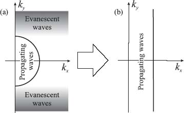
FIGURE 9.2 The fiber-optic effect by “TV rock, ” a mineral ulexite (NaCaB5O9·8H2O, hydrated sodium calcium borate hydroxide). (a) Top view. (b) Side view.
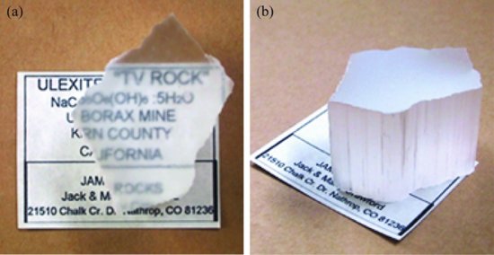
FIGURE 9.3 Photograph of the wire medium lens used in experiment [20]: 21×21 array of parallel 1 m long aluminum wires. The period of the array is 1 cm. The radius of the wires is 1 mm. The source in the form of a crown is adjacent to the front interface of the lens. The source is fed by a coaxial cable connected to a network analyzer. The small electric probe used for near-field scan is shown together with the supporting arm. Reprinted with permission from Reference 20. Copyright 2008 American Physical Society.
It is important to mention that the description of the wire medium using the permittivity model (9.4) is only a rough approximation. In reality, the wire medium is a spatially dispersive material and thus its electrodynamics is more complicated than suggested by Equation 9.4 [9]. However, for very long wavelengths the spatial dispersion effects are to some extent of second order [19], and the dielectric function (9.4) may describe fairly well the response of the material.
A planar wire medium slab (Fig. 9.3) enables the transformation of the near field produced by a source placed in the vicinity of the slab into propagating transmission line modes. These modes propagate along the direction normal to the interfaces and transfer the distribution of electric field from the front interface of the lens to the back interface without distortion, closely mimicking the behavior of a material with extreme anisotropy.
In a different but equivalent perspective, the slab of a wire medium may also be regarded as a bundle of very subwavelength waveguides performing pixel-to-pixel imaging. Each wire plays the role of a waveguide delivering information from one side of the lens to the other. The electric field distribution transported by a specific wire is approximately radial, and due to this reason the waveguides are nearly decoupled. This enables the propagation of waves along neighboring wires with a negligibly small interaction. The imaging resolution is approximately two periods of the wire medium [19], and, in principle, can be made as small as required by a given application.
In contrast to conventional lenses, near field lenses have to be placed in the close vicinity of the source in order to capture evanescent waves. Thus, it is important to ensure that the lens does not distort the source field distribution. An ideal near field lens should not produce any reflection. The problem of possible harmful reflections from a slab of a material with extreme anisotropy can be eliminated by properly choosing its thickness so that it operates as a Fabry–Perot resonator. The thickness should be equal to an integer number of half-wavelengths inside of the host material. In the case of an ideal material described by the dielectric function (9.4), the Fabry–Perot condition is verified simultaneously for all angles of incidence, including evanescent waves. This collective resonance makes the lens virtually transparent to any propagating or evanescent wave. This outstanding property is justified by the fact that all transmission line modes travel across the slab with the same phase velocity, irrespective of transverse wave vector. Thus, the total electrical length of the slab remains the same for all possible incidence angles.
A prototype of a 1 m long wire medium lens with 1 cm period is reported in Figure 9.3. The photograph shows the lens located in the anechoic chamber together with the setup for near field scan. The lens was designed to operate at frequencies around 150n MHz, which correspond to Fabry–Perot resonances of the nth order [20]. The measurements were made at frequencies around 900 and 1050 MHz corresponding to Fabry–Perot resonances of the 6th and 7th orders, respectively. This prototype is about seven times longer than the 15 cm long lens used for the preliminary experiments reported in References 21 and 22.
A wire antenna shaped as a crown was taken as the near field source. The source was placed near the front interface of the wire medium lens as shown in Figure 9.2, and the near field was scanned using an automatic mechanical planar near field scanner at a distance of 2 mm from the front and back interfaces of the lens (source and image planes). In order to confirm that the lens does not perturb or distort the near field of the source, the collected data were compared with the reference near field distributions obtained by scanning the near field created by the source in free space. The results of the near field scan at 898 and 1038 MHz are reported in Figures 9.4 and 9.5. A near field distribution reproducing the crown shape is clearly visible at the image plane. It is practically indistinguishable from the distributions in the source plane both with and without the presence of the wire medium lens. Despite the distance in-between the source and image planes at 898 and 1038 MHz being as large as 3 and 3.5 wavelengths, respectively, the imaging resolution is about two periods of the wire medium (2 cm), which in terms of the wavelength corresponds to λ/15. To the best of our knowledge, this is up to date the only demonstration of subwavelength imaging with such fine resolution over a distance much larger than the wavelength. In all other subwavelength imaging experiments reported in the literature, the distance between the source and image planes was only a small fraction of the wavelength, whereas the imaging resolution was much worse.
FIGURE 9.4 Results of the near field scan at the source plane (2 mm away from the front interface of the lens) without (left column) and with (central column) the wire medium lens and (right column) at the image plane (2 mm away from the back interface of the lens) at 890, 898, and 906 MHz.
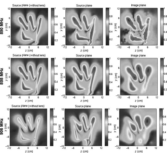
FIGURE 9.5 Results of the near field scan at the source plane (2 mm away from the front interface of the lens) without (left column) and with (central column) the wire medium lens and (right column) at the image plane (2 mm away from the back interface of the lens) at 1030, 1034 and 1038 MHz.
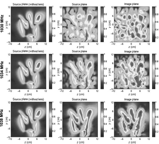
The near-field scan results reported in Figures 9.4 and 9.5 enable to clarify how the resolution of the wire medium lens depends on the frequency of operation. As mentioned before, the lens thickness is supposed to verify the Fabry–Perot condition. Actually, as it was shown in Reference 19, the best imaging is achieved at a frequency slightly below the Fabry–Perot condition. At higher frequencies subwavelength imaging is still observed, but with worse resolution. This can be clearly seen in Figure 9.4: The widths of the lines at the image plane become wider above the Fabry–Perot resonance. The amount of reflection provided by the wire medium slab at these frequencies is quite small: In Figure 9.4 the difference between the source plane distributions with and without the presence of the lens is not significant. These properties are typical of wire medium lenses [19, 22]. At frequencies below the Fabry–Perot resonance the imaging is disturbed by the excitation of surface waves at both the front and back interfaces of the lens. This effect can be clearly seen in Figure 9.5 where the image and the source plane field distributions in the presence of the lens at frequencies below Fabry–Perot resonance are completely distorted by the ripples caused by the excitation of surface wave modes [19, 22].
Despite the described dependency of the resolution on frequency, the resolving capabilities of wire medium lenses are reasonably wide-band. The actual bandwidth of operation depends on the complexity of the near field source and on its sensitivity to external fields [22], but it cannot be smaller than the fundamental theoretical limit formulated in Reference 19. In practice, a bandwidth of the order of a few percents is observed: 4.5% in Reference 22 for a half-wavelength thick lens with a complex meander-like source, and 2% in experiment with a 3 wavelength thick lens with a crown-shaped source [20]. For less complex sources the same lenses may provide much better bandwidth. For example, in Reference 21 the bandwidth was 18%, for a half-wavelength thick lens with a source shaped in the form of letter “P.”
In principle, the resolution of the wire medium lens can be made as fine as required by a specific application by just using materials with smaller periods. For example, instead of a lens with 1 cm period and wires with 1 mm radius (as in Fig. 9.3) providing resolution λ/15, one can manufacture a structure with 1 mm period and 100 μm radius of wires which would provide a resolution of λ/150 and so on.1 Basically, the minimum achievable resolution is limited only by the manufacturing capabilities and by the skin depth of the metal. In order to operate the wire medium in the canalization regime it is necessary that the radius of the rods is greater than the skin depth of the metal [23]. At microwaves, the skin depth of good metals is of the order of a few micrometers, and is thus negligible. The ultimate limit of resolution of wire medium lenses in different frequency regimes is discussed in Section 9.4.
9.3 MAGNIFYING AND DEMAGNIFYING LENSES WITH SUPER-RESOLUTION
Processing of subwavelength images, such as magnification or demagnification, can be performed by tapering the array of wires. Thus, by gradually increasing (decreasing) the spacing between wires from the front interface to the back interface, it is possible to magnify (demagnify) the subwavelength details of an image.
A numerical simulation of the tapered version of the 1 m lens described in Section 9.2 was performed using a commercial electromagnetic simulator based on the method of moments (MoM) [24]. The geometry of the structure is presented in Figure 9.6a. The spacing between the wires at the front interface is 1 cm (as in Fig. 9.3) and it gradually increases up to 3 cm at the back interface. The front and back interfaces of the lens are spherical surfaces with 50 and 150 cm radii, respectively. The lens is excited by a planar center-fed wire antenna in the form of letter “M, ” which is placed in the close vicinity of the front interface. The frequency of operation (910 MHz) is chosen slightly higher than the Fabry–Perot resonance of the 6th order (900 MHz) in order to achieve the best quality of imaging [25].
FIGURE 9.6 (a) Geometry of the magnifying wire medium lens excited by a planar near field source shaped as the letter “M.” The distance between the source and the center of the front interface is 13 mm. All the length dimensions in the figure are given in millimeters. Calculated distributions of the electric field normal component: (b) on a planar surface located (13+8) mm away from the lens input interface (the reference plane is displaced 8 mm from the source) and (c) on a spherical surface displaced 15 mm from the output interface. The frequency of operation is 910 MHz. Reprinted with permission from Reference 20. Copyright 2008 American Physical Society.
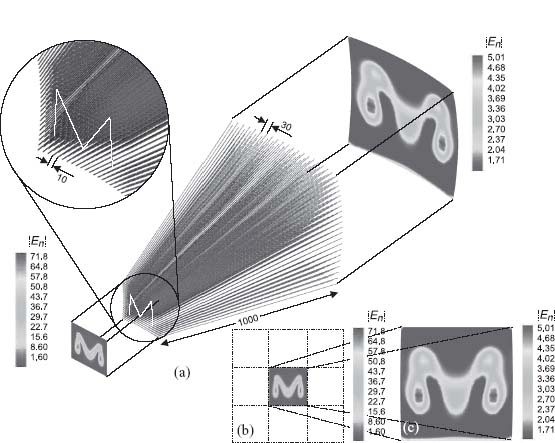
This structure enables a threefold magnification of the source. This fact is clearly seen in Figures 9.6b and 9.6c where the distributions of the normal (with respect to the interface) component of electric field at 8 mm distance from the source and 15 mm distance from the back interface are plotted. The distance in-between the source and the image is about 3 wavelengths. In both figures a sharp near field distribution in the form of the letter M is visible, but remarkably the image is magnified three times as compared to the original. A larger magnification is possible with a similar structure, but it requires the use of a thicker lens.
The proposed tapered lens (Fig. 9.6a) has spherical input and output interfaces, but some applications may require the use of planar interfaces. The difficulty of making a tapered lens with planar interfaces is that it inevitably requires the use of wires with different physical lengths. This may destroy the collective Fabry–Perot resonance and affect the performance of the lens. However, returning to the explanation that each wire of the lens operates as a separate subwavelength waveguide, one can conclude that the physical length of the wires does not really matter, provided its electrical length is invariant. Thus, provided the electrical length of the wires in a tapered lens with planar interfaces is constant, the lens may still operate as desired. One interesting possibility to make this phase compensation is to incorporate a properly shaped dielectric block inside of the lens [26].
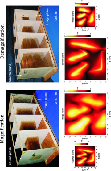
If the variation of lengths of rods in the lens is not significant as compared to the wavelength then the distortions are minimal. The experimental demonstration of this fact has been performed in Reference 27. A tapered wire medium lens has been constructed (see Fig. 9.7) and both threefold magnification and threefold demagnification with subwavelength resolution were demonstrated. The results of near field scans in the source and image planes presented in Figure 9.7 clearly demonstrate the performance of the device.
FIGURE 9.7 Magnification and demagnification experiments with tapered array of brass wires. The geometries of the lenses and the near field distributions in the source and image planes are shown. The frequency of operation for magnification regime is 1047 MHz and for demagnification 455 MHz. Reprinted with permission from Reference 27. Copyright 2010 American Institute of Physics.
Magnifying lenses are expected to find immediate application in near field microscopy as near field to far-field transformers [4–7] since they may allow mapping field distributions with subwavelength details into images with details larger than the wavelength, which can be processed using conventional diffraction-limited imaging techniques. Also, tapered lenses may be used for demagnification of images if the source and image interfaces of the magnifying lens are interchanged. Demagnifying lenses may allow creating complex near field distributions from enlarged copies created in the far field. On this route, it may be possible to create extremely compact near field spots which can be used for dense writing of information on various media, in the same manner as diffraction-limited laser spots are currently used for writing on DVD drives.
Tapered wire medium lenses, especially in the terahertz range, can be regarded as multipixel endoscopes capable of performing direct and inverse manipulations with the electromagnetic fields in the subwavelength spatial scale: capturing an electromagnetic field profile created by deeply subwavelength objects at the endoscope’s tip and magnifying it for observation, or projecting a large mask at the endoscope’s base onto a much smaller image at the tip [28].
In the microwave range the tapered wire medium endoscopes may be possibly applied for the improvement of magnetic resonance imaging (MRI) systems [29]. Such systems use small magnetic probes, whose dimensions determine the resolution of MRI. To ensure a reasonable efficiency the probes cannot be made much smaller than the wavelength. This obviously restricts the resolution of these systems. By placing the tapered wire medium lenses in-between the object under test and the probe of the near field scanner, it may be possible to further reduce the effective size of the probe keeping its efficiency at the same level, and improving in this way the resolution of MRI. Likewise, tapered wire medium endoscopes and lenses can be used to enhance the performance of other mechanical near field microwave scanners suffering from similar problems. Instead of attempting to use small probes in order to improve resolution one can magnify the near field distribution under test and detect the magnified distribution using a conventional probe. It is envisioned that the tapered lenses can be used in two ways: The tapered endoscope can be attached to the probe effectively reducing its size (in this case the scan is performed along the surface under test using the tip of the endoscope) or a large tapered lens can be attached to the whole sample under test and the magnified near field distribution is scanned at the output interface of the lens.
9.4 IMAGING AT THE TERAHERTZ AND INFRARED FREQUENCIES
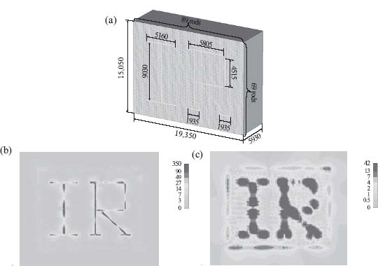
The wire medium lenses described in the previous sections were designed to operate at the microwave frequency range. However, the structures may be easily scaled up to terahertz and even infrared frequencies provided the metal used to fabricate the rods maintains reasonable conductive properties. For example, in Reference 30 it was reported that a wire medium lens made of silver (Ag) nanorods enables subwavelength resolution of λ/10 at 30 THz (λ = 10 μm). Figure 9.8 shows the results reported in Reference 30 for imaging at 31 THz.
FIGURE 9.8 Numerical modeling of subwavelength imaging at 31 THz (λ = 10 μm) [30]. (a) Geometry of the lens: a square array with 215 nm period formed by silver nanorods with 21.5 nm radius embedded into a block of chalcogenide glass (relative permittivity  = 2.2). All dimensions in the figure are given in nanometers. The lens is excited by a planar antenna shaped in the form of the letters “IR, ” and located 107.5 nm apart from the front interface of the lens. Calculated distributions of the normal component of electric field: (b) at the front interface (source plane) and (c) at the back interface (image plane). Reprinted with permission from Reference 30. Copyright 2007 American Physical Society.
The main difficulty with the extension of the wire medium lens concept to the terahertz and infrared regimes is that most metals do not exhibit strong conductive properties at these frequencies, but instead have a plasmonic response. This fact imposes some constraints on the implementation of the canalization regime at the infrared range using arrays of nanorods [30]. As demonstrated in Reference 23, for real metals (with finite conductivity) the resolution of the “wire medium lens” cannot be further improved by reducing the spacing between the wires after the radius of the wires becomes smaller than the skin depth of the metal. In addition, for geometrical reasons the period of the array should be at least two times larger than the radius of rods. Since the resolution of a lens operated in the canalization regime is approximately two times the spacing between the wires [19], we can estimate that the ultimate physical limit of resolution of wire medium lenses is about four times the skin depth of the metal.
Table 9.1 Ultimate Limit of Resolution of Wire Medium Slabs for Several Metals and Frequencies
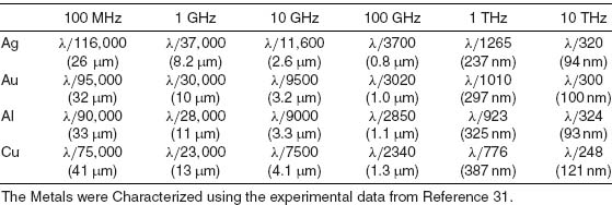
To give an idea of the possibilities, the limits of resolution yielded by rods of silver (Ag), gold (Au), aluminum (Al), and copper (Cu) at several frequencies are compiled in Table 9.1. It was assumed that the metals are described by a Drude model with the plasma and damping frequencies as in References 31 and 32. It is seen that at microwave frequencies the ultimate limit of resolution is several orders of magnitude larger than the classical diffraction limit, and that the best results are achieved with silver. Even at terahertz frequencies the resolution may be of the order of λ/300. In particular, one may conclude that at the terahertz range, arrays of parallel rods made of noble metals and their tapered versions may enable the same manipulations in the subwavelength spatial scale as their microwave counterparts (Figs. 9.3 and 9.6a). The only difference is that the structures for the terahertz range are more difficult to fabricate.
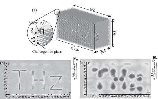
To illustrate the potentials of wire medium lenses at terahertz frequencies, we consider the structure depicted in Figure 9.9a. The lens is formed by an array of silver nanorods supported by a block of chalcogenide glass, which has low losses at terahertz frequencies. The source antenna is shaped as the letters “THz” in order to emphasize the frequency of operation: 5 THz. The performance of the lens was simulated using the commercial electromagnetic solver [33]. The calculated near field distributions at the front and back interfaces are presented in Figures 9.9b and 9.9c, respectively. The letters “THz” are clearly visible in both distributions. The effect of realistic losses in silver at 5 THz [31, 32] was fully taken into account in the simulation. In this example the radius of the rods R was chosen so that R = 4.8δ (δ is the skin depth of silver), which enables very good imaging. The resolution in this example is λ/23 (2.6 μm) and the image is formed at a distance 0.65λ (38.8 μm) from the source.
FIGURE 9.9 Numerical modeling of subwavelength imaging at 5 THz (λ = 60 μm) [23]. (a) Geometry of the lens: a square array with 1.3 μm period formed by silver nanorods with 130 nm radius embedded into a block of chalcogenide glass (relative permittivity  = 2.2). All dimensions in the figure are given in micrometers. The lens is excited by a planar antenna shaped in the form of the letters “THz” and located 650 nm apart from the front interface of the lens. Calculated distributions of the normal component of electric field: (b) at the front interface (source plane) and (c) at the back interface (image plane).
Interestingly, high losses in the rods material may not affect the imaging performance provided the absolute value of permittivity is large enough. This happens because the field canalized through the lens is mainly concentrated in the host material in-between the rods. It is extruded from the rods because of their high permittivity. This means that extremely lossy materials, for example, materials operated near absorption bands, may also be good candidates for the realization of wire media with extreme anisotropy.
Regarding fabrication issues, it has to be noted that the realization of wire medium lenses does not need to be very precise. The lens performance is not sensitive to the exact locations of the rods in the matrix, variations of the radii of the rods, or the precise shape of the rods cross section. The only parameter that it is necessary to control is the length of the rods. It should be roughly the same for all rods, and the rods need to be continuous. Broken rods or rods with conductivity defects may significantly affect the imaging quality.
An experimental demonstration of subwavelength imaging by array of metallic nanorods in the infrared range has been performed in Reference 34. A manufactured nanolens consisted of aligned gold nanowires, with 12 nm diameters and lattice spacing of 25 nm, embedded in 10 μm thick porous alumina template matrix. Figure 9.10 shows the near field optical microscope scans in the source and image planes at 1550 nm wavelength. It is clear that the subwavelength details of the source were transmitted to the image plane with λ/4 resolution over 5λ distance. The manufacturing of nanolenses using porous alumina templates is a very prospective technique for mass production since it uses chemical processes and self-organization mechanisms at the nanoscale which are quite cheap and well established.
FIGURE 9.10 (a) Imaging with subwavelength resolution by the metamaterial nanolens at 1550 nm. The nanolens consists of high aspect ratio metallic nanowires which are embedded in a host dielectric medium. This bulk metamaterial transports subwavelength details of an object at a significant distance of more than six times the wavelength (λ). (b) Scanning electron microscope (SEM) image of the NEU letters (acronym for Northeastern University) milled in 100 nm thick gold metallic film. The letters have 600 nm wide arms (0.4λ). (c) near field scanning optical microscope (NSOM) scan of the source object in the near field at 1550 nm wavelength. (d) NSOM scan of the corresponding image by the metamaterial nanolens above the nanolens surface. Reprinted with permission from Reference 34. Copyright 2010 American Institute of Physics.
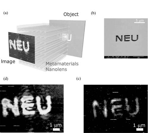
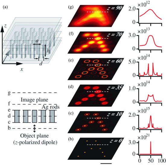
FIGURE 9.11 Subwavelength plasmonic image transfer of a character pattern “λ” with a metallic nanorod array device [35]. (a) The structural model of the device, which is constructed by hexagonally arranged silver nanorods of 20 nm diameter, 50 nm height, and 40 nm pitch, respectively. (b–g) Field propagation process in the image transfer obtained at each longitudinal position by the FDTD simulation. The character pattern is composed of an array of z-polarized dipoles. Left-side images show the cross-sectional intensity distributions in the x–y plane. The plots on the right side show the cross-sectional line profiles of dashed lines in the left images. The object plane and imaging plane are defined as z = 0 and z = 70 nm. The operation wavelength is 488 nm. The size of the scale bar is 50 nm. Reprinted with permission from Reference 35. Copyright 2005 American Physical Society.
9.5 NANOLENSES FORMED BY NANOROD ARRAYS FOR THE VISIBLE FREQUENCY RANGE
In the visible frequency range it may also be possible to achieve subwavelength imaging using metallic nanorods [35]; see Figure 9.11. This possibility is based on the excitation of surface plasmon-polaritons in the metallic rods. However, this regime is highly sensitive to losses and may introduce important phase and amplitude distortions in the image due to the harmful interaction among surface plasmons traveling along adjacent rods. In particular, this may result in the impossibility of resolving certain source field distributions at the image plane.
The nanorod array proposed in Reference 35 operates with incoherent sources and does not image properly coherent sources with certain phase distributions. This happens because the length of nanorods is not properly chosen for imaging at the wavelength of interest. It has been shown in Reference 36 that the proper choice of the nanorod length (so that the length obeys Fabry–Perot resonance condition and thus, the lens operates in canalization regime) makes possible to image arbitrary coherent sources with the same geometry of nanorod array. Figure 9.12 shows how the subwavelength imaging performance of the nanolens depends on the length of the nanorods. The image of six coherent point sources obtained with 50 nm long nanorods replicates the result of Reference 35 and does not represent the original source field distribution. The image that closely mimics the source is the one obtained with 80 nm long rod—this is an optimal length of the nanorod. The field distributions at the image plane obtained with 60, 70, and 90 nm rods give us a misleading vision of source comprised of seven dipoles for a bright point, besides the six that represent the source, at the center is discerned. However, 50 and 100 nm rods give us an impression of a source formed of a single dipole located at the center of the hexagon. The detailed analysis [37] revealed that the lens formed by 80 nm long nanorods is not sensitive to the form of source (the original lens [35] was operating only with sources formed by dipoles located at the axes of the nanorods) and offers about 10% bandwidth of operation.
FIGURE 9.12 (a) Geometry of the finite array of silver nanorods with triangular-lattice arrangement. The point coherent sources are aligned with the axis of the nanorod and are placed at a distance 10 nm away from array interface. The diameter of the nanorods is d = 20 nm, the period of the structure is a = 40 nm. The length of nanorods L is varied. (b) Source and image plane field distribution for various lengths of the nanorod at 488 nm wavelength. The normal component of electric field is sampled at the front interface of the nanolens and across a plane 10 nm away from back interface, respectively. Reprinted with permission from Reference 36. Copyright 2010 American Physical Society.
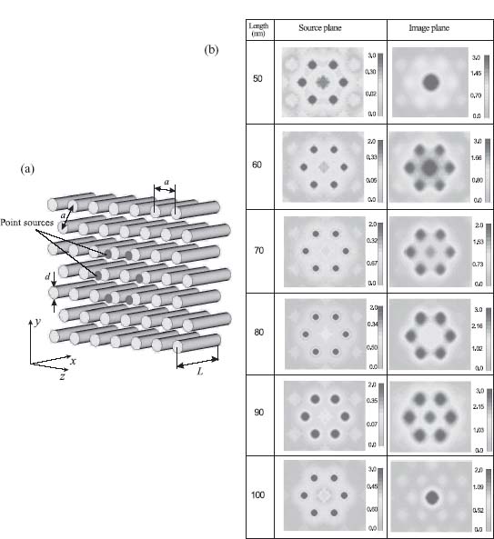
FIGURE 9.13 Long-distance image transfer realization through a stacked arrangement of nanorod arrays. (a) The basic concept of the stacked arrangement of nanorod arrays for long-distance image transfer. In this example, a three-layered stacked arrangement is presented. The image of the letter A is obtained from simulations based on 3D-FDTD calculations. (b) Intensity profiles across 3-, 9-, and 17-layered stacked arrays, showing that neither intensity nor the point spread function has any noticeable dependence on distance, at least up to micrometer-scale distances. The inset shows the line width of the point spread function at the exit of 17 layers. Reprinted with permission from Reference 38. Copyright 2008 Macmillan Publishers Limited.
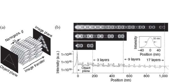
An interesting idea of long-distance transport of color images with subwavelength resolution was proposed in Reference 38. It has been proposed to use multi-segment array of nanorods for transmission of subwavelength images to longer distances as compared to single-nanorod arrays [35–37] by virtue of the so-called domino plasmon effect; see Figure 9.13. The multisegment nanolens offers an attractive possibility of subwavelength imaging in a wide range of frequencies (color imaging) with incoherent sources [38]. The imaging capabilities of the stacked nanolens with coherent sources was studied in Reference 39. The gap between consecutive segments and the length of the nanorod allows to tune the nanolens to operate at a particular frequency in a similar manner as in Reference 36. The typical bandwidths of 3 and 1.5% were observed for three- and six-segment nanolenses, respectively. However, despite all the positive traits for the performance of stacked nanolenses, the color imaging of coherent sources remains elusive.
9.6 SUPERLENSES AND HYPERLENSES FORMED BY MULTILAYERED METAL–DIELECTRIC NANOSTRUCTURES
In the visible frequency range there is an interesting alternative opportunity to create extremely anisotropic material (9.4) without employing metallic nanorods. This can be achieved by using multilayered metal–dielectric nanostructures [40]. Let us consider a layered structure presented in Figure 9.14.
FIGURE 9.14 Geometry of layered metal–dielectric metamaterial.
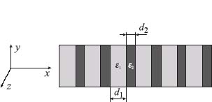
Such a metamaterial can be described using permittivity tensor of the form
where

In order to get  and
and  and obtain a material with permittivity tensor of the form (9.4), required for implementation of the canalization regime, it is necessary to choose parameters of the layered material so that
  1/
1/ 2 = –d1/d2 and
  1 +
1 +  2 = 1. From the first equation it is clear that one of the layers should have negative permittivity and thus the structure has to be formed by one dielectric layer and one metallic layer. For example, one can choose
  1 = 2,
  2 = –1, and d1/d2 = 2, or
  1 = 15,
  2 = –14, and d1/d2 = 15/14.
Note that no layered structure required for canalization regime can be formed using equally thick layers d1 = d2. The layered metal–dielectric structures considered in References 41–43 have completely different properties. As it is noted in Reference 43, the structures with d1 = d2 and  1 = –
1 = – 2 correspond to
 = 0 and
  and operate in tunneling regime as an array of wires embedded into the medium with zero permittivity. The absence of matching causes strong reflections and restricts slab thickness to be thin. More details about differences between canalization and tunneling regimes in multilayered metal–dielectric structures are available in References 44 and 45.
The canalization regime implementation using the suggested metal–dielectric layered structure has been demonstrated in Reference 11 numerically using CST Microwave Studio package [33]. A subwavelength source (a loop of the current in the form of letter P) is placed at 20 nm distance from a 300 nm thick multilayer slab composed of 10 and 5 nm thick layers with  1 = 2 and
  2 = –1, respectively. The detailed geometry of the structure is presented in Figure 9.15. The wavelength of operation λ is 600 nm. The metal with
  = –1 at 600 nm wavelength can be created by doping some lossless dielectric by a small concentration of silver which has
  = –15 at such frequencies, in a similar manner to the ideas of works [46, 47].
FIGURE 9.15 Geometry of transmission device formed by a layered metal–dielectric metamaterial: (a) perspective view, (b) side view, (c) front view, (d) small details. All dimensions are in nanometers. Reprinted with permission from Reference 11. Copyright 2006 American Physical Society.
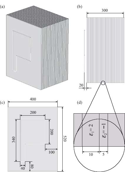
FIGURE 9.16 Distributions of absolute value normal to the interface component of electrical field (arbitrary units): (a) in free space, 20 nm from source; (b) at the front interface; (c) at the back interface; (d) in free space, 20 nm from back interface.
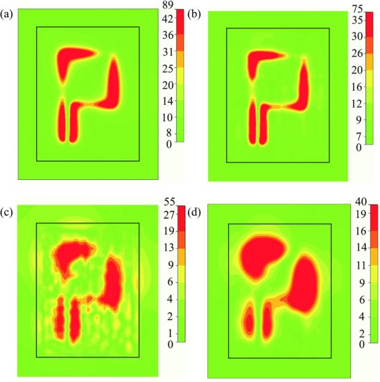
The field distributions in the planes parallel to the interface of the structure plotted in Figure 9.16 clearly demonstrate imaging with 30 nm resolution (λ/20). Figure 9.16a shows the field produced by the source in free space at 20 nm distance. It is practically identical to the field observed at the front interface of the structure (Fig. 9.16b). It confirms that the reflections from the front interface are negligibly small. Actually, the main contribution to the reflected field comes from diffraction at corners and wedges of the device. Figure 9.16c shows the field at the back interface of the structure. The image is clearly visible, but it is a little bit distorted by plasmon-polariton modes excited at the back interface. Being diffracted into the free space this distribution forms an image without distortions produced by plasmon-polariton modes; see Figure 9.16d presenting field distribution at 20 nm distance from the back interface.
The resolution of the proposed layered structure is restricted by its period d = d1 + d2. The model of uniaxial dielectric 1.5 is valid only for a restricted range of wave-vector components. In order to illustrate this an isofrequency contour for the layered structure considered as 1D photonic crystal was calculated using an analytical dispersion equation available in Reference 48. The result is presented in Figure 9.17. While |qzd/π| < 0.5 the isofrequency contour is flat, the homogenized model (9.5) is valid, and the structure operates in the canalization regime. The spatial harmonics which have |qzd/π| > 0.5 will be lost by the device and this defines d/0.5 ≈ λ/20 resolution. The calculation of isofrequency contour for the case of  1 = 15,
  2 = –14, d1 = 7.76 nm, and d2 = 7.24 nm for the same wavelength of 600 nm revealed its flatness for |qxd/π| > 1.5. This allows us to predict d/1.5 ≈ λ/60 resolution for this case. The last structure can be constructed using silicon as dielectric and silver as metal, but very accurate fabrication with error no more than 0.05 nm will be required in order to get proper result. The losses in silver in both cases are already reduced by operating at a rather long wavelength of 600 nm, but in accordance with our estimations they are still high enough to destroy the quality of the subwavelength resolution. This problem can be solved by using active materials [49], for example, doped silicon [43, 46]. The optimal parameters for different constituent materials of the metal–dielectric structure are available in Reference 50. The general study of limitations on homogenization of periodic layered structures is provided in References 48 and 51.
FIGURE 9.17 Isofrequency contour of layered metal–dielectric structure with  1 = 2,
  2 = –1, d1 = 10 nm, d2 = 5 nm, d = d1 + d2 = 15 nm for λ = 600 nm. The region where the dispersion curve is flat (|qzd/π| < 0.5) is shadowed. Reprinted with permission from Reference 11. Copyright 2006 American Physical Society.
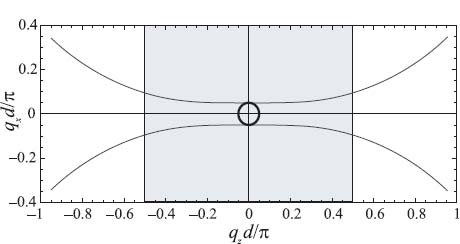
FIGURE 9.18 Hyperlenses. (a) Prism geometry. (b) Cylindrical geometry. Reprinted with permission from Reference 4. Copyright 2006 American Physical Society.
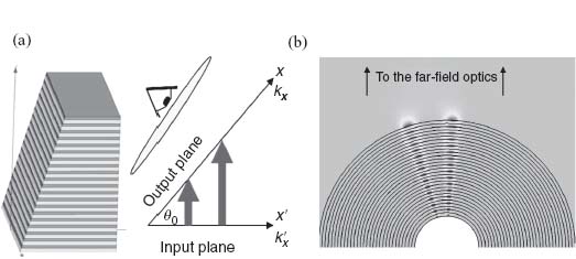
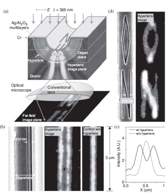
FIGURE 9.19 Magnifying optical hyperlens. (a) Schematic of hyperlens and numerical simulation of imaging of subdiffraction-limited objects. (b) Hyperlens imaging of line pair object with line width of 35 nm and spacing of 150 nm. From left to right, scanning electron microscope image of the line pair object fabricated near the inner side of the hyperlens, magnified hyperlens image showing that the 150-nm-spaced line pair object can be clearly resolved, and the resulting diffraction-limited image from a control experiment without the hyperlens. (c) The averaged cross section of hyperlens image of the line pair object with 150 nm spacing (red), whereas a diffraction-limited image obtained in the control experiment (green). A.U., arbitrary units. (d) An arbitrary object ON imaged with subdiffraction resolution. Line width of the object is about 40 nm. The hyperlens is made of 16 layers of Ag/Al2O3. Reprinted with permission from Reference 7. Copyright 2007 American Association for the Advancement of Science.
The magnifying and demagnifying lenses with subwavelength resolution (hyperlenses, see Section 9.3) formed by layered metal–dielectric nanostructures were proposed simultaneously in References 4 and 5. There are two types of hyperlenses: prism-like superlens and cylindrical superlens (see Fig. 9.18). The cylindrical hyperlens found more applications as compared to prism-like one since every point of its aperture experiences the same transmission characteristic independently of the level of losses in the structure. The cylindrical hyperlenses are using the same principle of operation as the canalization regime, but in order to avoid distortions of the image the thicknesses of the layers have to be tuned accordingly [52].
An experimental demonstration of subwavelength imaging at 365 nm wavelength with 40 nm resolution by hyperlens formed by silver and alumina layers was demonstrated in Reference 7; see Figure 9.19.
REFERENCES
1. Pendry JB (2000) Negative refraction index makes perfect lens. Phys. Rev. Lett. 85: 3966–3969.
2. Fang N, Lee H, Sun C, Zhang X (2005) Subdiffraction-limited optical imaging with a silver superlens. Science 308: 534–537.
3. Narimanov EE, Shalaev VM (2007) Beyond diffraction. Nature 447: 266–267.
4. Salandrino A, Engheta N (2006) Far-field subdiffraction optical microscopy using metamaterial crystals: theory and simulations. Phys. Rev. B 74: 075103.
5. Jacob Z, Alekseyev LV, Narimanov E (2006) Optical hyperlens: far-field imaging beyond the diffraction limit. Opt. Express 14: 8247–8256.
6. Smolyaninov II, Hung Y-J, Davis CC (2007) Magnifying superlens in the visible frequency range. Science 315: 1699–1701.
7. Liu Z, Lee H, Xiong Y, Sun C, Zhang X (2007) Far-field optical hyperlens magnifying sub-diffraction-limited objects. Science 315: 1686.
8. Westphal V, Hell SW (2005) Nanoscale resolution in the focal plane of an optical microscope. Phys. Rev. Lett. 94: 143903.
9. Belov PA, Marques R, Maslovski SI, Nefedov IS, Silverinha M, Simovski CR, Tretyakov SA (2003) Strong spatial dispersion in wire media in the very large wavelength limit. Phys. Rev. B 67: 113103.
10. Silveirinha M (2006) Nonlocal homogenization model for a periodic array of epsilon-negative rods. Phys. Rev. E 73: 046612.
11. Belov PA, Hao Y (2006) Subwavelength imaging at optical frequencies using a transmission device formed by a periodic layered metal-dielectric structure operating in the canalization regime. Phys. Rev. B 73: 113110.
12. Belov PA, Simovski CR, Ikonen P (2005) Canalization of sub-wavelength images by electromagnetic crystals. Phys. Rev. B. 71: 193105.
13. Podolskiy VA, Narimanov EE (2005) Near-sighted superlens. Opt. Lett. 30: 75–77.
14. Yen TJ, Padilla WJ, Fang N, Vier DC, Smith DR, Pendry JB, Basov DN, Zhang Z (2004) Tetrahertz magnetic response from artificial materials. Science 303: 1494–1496.
15. Linden S, Enkrich C, Wegener M, Zhou J, Kochny T, Soukoulis C (2004) Magnetic response of metamaterials at 100 terahertz. Science 306: 1351–1353.
16. Zhang S, Fan W, Panoiu NC, Malloy KJ, Osgood RM, Brueck SRJ (2005) Experimental demonstration of near-infrared negative-index metamaterials. Phys. Rev. Lett. 97: 137404.
17. Shalaev VM (2007) Optical negative-index metamaterials. Nat. Photonics 1: 41–48.
18. Ikonen P, Belov PA, Simovski CR, Maslovski SI (2006) Experimental demonstration of subwavelength field channeling at microwave frequencies using a capacitively loaded wire medium. Phys. Rev. B 73: 073102.
19. Belov PA, Silveirinha MG (2006) Resolution of sub-wavelength lenses formed by a wire medium. Phys. Rev. E 73: 056607.
20. Belov PA, Zhao Y, Tse S, Ikonen P, Silveirinha MG, Simovski CR, Tretyakov SA, Hao Y, Parini C (2008) Transmission of images with subwavelength resolution to distances of several wavelengths in the microwave range. Phys. Rev. B 77: 193108.
21. Belov PA, Hao Y, Sudhakaran S (2006) Subwavelength microwave imaging using an array of parallel conducting wires as a lens. Phys. Rev. B 73: 033108.
22. Belov PA, Zhao Y, Sudhakaran S, Alomainy A, Hao Y (2006) Experimental study of the sub-wavelength imaging by a wire medium slab. Appl. Phys. Lett. 89: 262109.
23. Silveirinha MG, Belov PA, Simovski CR (2008) Ultimate limit of resolution of subwavelength imaging devices formed by metallic rods. Opt. Lett. 33: 1726–1728.
24. FEKO Suite 5.2, EM SOftware & Systems - SA (Pty) Ltd, http://www.feko.info.
25. Ikonen P, Simovski C, Tretyakov S, Belov P, Hao Y (2007) Magnification of subwavelength field distributions at microwave frequencies using a wire medium slab operating in the canalization regime. Appl. Phys. Lett. 91: 104102.
26. Zhao Y, Palikaras G, Belov PA, Dubrovka RF, Simovski CR, Hao Y, Parini CG (2010)t Magnification of subwavelength field distributions using a tapered array of metallic wires with planar interfaces and an embedded dielectric phase compensator. New J. Phys. 12: 103045.
27. Belov PA, Palikaras GK, Zhao Y, Rahman A, Simovski CR, Hao Y, Parini C (2010) Experimental demonstration of multiwire endoscopes capable of manipulating near fields with subwavelength resolution. Appl. Phys. Lett. 97: 191905.
28. Shvets G, Trendafilov S, Pendry JB, Sarychev A (2007) Guiding, focusing, and sensing on the subwavelength scale using metallic wire arrays. Phys. Rev. Lett. 99: 053903.
29. Radu X, Dardenne X, Craeye C (2007) Experimental results and discussion of imaging with a wire medium for mri imaging applications. In: Proceedings of IEEE Antennas and Propagation Society International Symposium. pp 5499–5502.
30. Silveirinha MG, Belov PA, Simovski CR (2007) Sub-wavelength imaging at infrared frequencies using an array of metallic nanorods. Phys. Rev. B 75: 035108.
31. Ordal MA, Bell RJ, Alexander RW, Long LL, Querry MR (1985) Optical properties of fourteen metals in the infrared and far infrared: Al, Co, Cu, Au, Fe, Pb, Mo, Ni, Pd, Pt, Ag, Ti, V, and W. Appl. Opt. 24: 4493–4499.
32. El-Kady I, Sigalas MM, Biswas R, Ho KM, Soukoulis CM (2000) Metallic photonic crystals at optical wavelengths. Phys. Rev. B 62: 15299–15302.
33. CST Microwave Studio 2006, CST GmbH, http://www.cst.com.
34. Casse BDF, Lu WT, Huang YJ, Gultepe E, Menon L, Sridhar S (2010) Super-resolution imaging using a three-dimensional metamaterials nanolens. Appl. Phys. Lett. 96: 023114.
35. Ono A, Kato J, Kawata S (2005) Subwavelength optical imaging through a metallic nanorod array. Phys. Rev. Lett. 95: 267407.
36. Rahman A, Belov PA, Hao Y (2010) Tailoring silver nanorod arrays for subwavelength imaging of arbitrary coherent sources. Phys. Rev. B 82: 113408.
37. Rahman A, Kosulnikov SYu, Hao Y, Parini C, Belov PA (2011) Subwavelength optical imaging with an array of silver nanorods. J. Nanophotonics 5: 051601.
38. Kawata S, Ono A, Verma P (2008) Subwavelength colour imaging with a metallic nanolens. Nat. Photonics 2: 438–442.
39. Voroshilov PM, Rahman A, Kivshar YS, Belov PA (2011) Efficiency of subwavelength imaging with multisegment nanolens. J. Nanophotonics 5: 053516.
40. Shen JT, Catrysse PB, Fan S (2005) Mechanism for designing metallic metamaterials with a high index of refraction. Phys. Rev. Lett. 94: 197401.
41. Shamonina E, Kalinin VA, Ringhofer KH, Solymar L (2001) Imaging, compression and Poynting vector streamlines for negative permittivity materials. Electron. Lett. 37: 1243–1244.
42. Anantha Ramakrishna S, Pendry JB, Wiltshire MCK, Stewart WJ (2003) Imaging the near field. J. Mod. Opt. 50: 1419–1430.
43. Anantha Ramakrishna S, Pendry JB (2003) Removal of absorption and increase in resolution in a near field lens via optical gain. Phys. Rev. B 67: 201101.
44. Li X, He S, Jin Y (2007) Subwavelength focusing with a multilayered Fabry-Perot structure at optical frequencies. Phys. Rev. B 75: 045103.
45. Kotynski R, Stefaniuk T (2009) Comparison of imaging with sub-wavelength resolution in the canalization and resonant tunnelling regimes. J. Opt. A Pure Appl. Opt. 11: 015001.
46. Garcia de Abajo FJ, Gomez-Santos G, Blanco LA, Borisov AG, Shabanov SV (2005) Tunneling mechanism of light transmission through metallic films. Phys. Rev. Lett. 95: 067403.
47. Cai W, Genov DA, Shalaev VM (2005) Superlens based on metal-dielectric composite. Phys. Rev. B 72: 193101.
48. Orlov AA, Voroshilov PM, Belov PA, Kivshar YuS (2011) Engineered optical nonlocality in nanostructured metamaterials. Phys. Rev. B 84: 045424.
49. Vincenti MA, de Ceglia D, Rondinone V, Ladisa A, D’Orazio A, Bloemer MJ, Scalora M (2009) Loss compensation in metal-dielectric structures in negative-refraction and super-resolving regimes. Phys. Rev. A 80: 053807.
50. Pastuszczak A, Kotynski R (2011) Optimized low-loss multilayers for imaging with sub-wavelength resolution in the visible wavelength range. J. Appl. Phys. 109(8): 084302.
51. Chebykin AV, Orlov AA, Vozianova AV, Maslovski SI, Kivshar YuS, Belov PA (2011) Nonlocal effective medium model for multilayered metal-dielectric metamaterials. Phys. Rev. B 84: 115438.
52. Kildishev AV, Narimanov EE (2007) Impedance-matched hyperlens. Opt. Lett. 32: 3432–3434.
1 However, one should keep in mind that to take advantage of a lens with a better resolution the source may need to be placed closer to the front interface.


