10
Active and Tuneable Metallic Nanoslit Lenses
10.1 INTRODUCTION
In diffractive optics, typical feature sizes are on the order of the wavelength, which is around 1 μm for visible and near-infrared light. Although nanometer-scale features do not diffract optical waves, nanosized structures could enable us to design novel diffractive optical devices. Plasmonics and metamaterials are the two ways to couple light into nanoscale. Plasmonics allow the coupling of light with a free-electron gas, thus generating oscillation modes known as plasmons. Metamaterials can be used to create artificial electromagnetic spaces characterized by effective permittivities and permeabilities. In this chapter, we focus our discussion on diffraction lenses made of arrays of nanoslits milled in metallic films. We show that diffraction lenses could go beyond classical optics with plasmonics and metamaterials.
One way to take advantage of plasmonic materials is to make waveguides out of them. In plasmonic waveguides, light propagates as a surface plasmon polariton (SPP) which is nanoscale in size and oscillates at a few hundreds of terahertz. Plasmonic waveguides have the potential to help solve the problem of ever-increasing demand for smaller and faster communication devices. In the design of our nanoslit lenses, we utilize the unique dispersion features of plasmonic waveguides.
Among optical metamaterials [1], a unique class of metal–dielectric lamellar structures called hyperbolic metamaterials (HMMs) have received much recent attention. An HMM has strong uniaxial anisotropy where the principal elements of the permittivity tensor have opposite signs. Hence, the isofrequency curve of hyperbolic media is a hyperbola; this is different from an anisotropic dielectric whose dispersion is ellipsoidal. As a consequence of their hyperbolic dispersion, HMMs theoretically could possess many unique properties such as unbounded effective refractive index and super-resolution capabilities. When subwavelength slits are combined with HMMs, the diffractive nature becomes drastically different from diffraction in free space. For example, inside an HMM, the propagation of diffracted light from a nanoslit is highly directional. By utilizing this unique feature, focusing is possible with a subwavelength spot size [2].
The initial devices based on plasmonics and metamaterials were passive, and thus their functionalities were determined by the initial designs and the materials. As these research fields continue to mature, the demands for the devices to be active and tuneable became much stronger for practical and engineering applications. Therefore, we present our results on active nanoslit lenses and tuneable nanoslit lenses in the following sections. Since plasmonic and metamaterial devices use metals whose losses are not negligible, it is of critical interest to develop active devices. In our chapter, we study the possibility of loss compensation of the HMMs by including a gain medium in the design. When modeling the dispersions of HMMs, we tested four different methods that are commonly used in the community.
We have organized the chapter in the following way. We begin by presenting our recent work on planar plasmonic diffractive focusing devices which consist of arrays of nanoslits milled in gold films [3]. Our planar nanoslit metal lenses work for both TM and TE polarizations and can emulate both convex and concave conventional dielectric lenses. We give a brief overview on the experimental characterization and full-wave numerical simulations of light propagation in the fabricated prototypes. Next we show that the focusing properties of nanoslit lenses can be externally tuned by filling the slits with index-changing materials such as a liquid crystal (LC) material. Using LCs, we can control the focal intensity [4] of the device. With a different index-changing material, in this case a nonlinear medium, we can shift the focal length [5] of the nanoslit lens. Finally, we discuss our work on HMM-assisted nanoslit devices for subwavelength focusing. A case study on active HMM dispersions is provided and discussed [6], followed by the numerical simulations of subwavelength diffraction with active HMMs [7] and the experimental demonstration of subwavelength diffraction with a passive HMM [8].
10.2 POLARIZATION-SELECTIVE GOLD NANOSLIT LENSES
The performance of diffraction optics can be improved by using noble metals in the visible spectral range. When light propagates through metallic apertures (e.g., slits, holes), SPP modes can be generated and used in diffraction lenses. The wavevectors of the SPP mode depend on the dimensions of the apertures. This allows for very flexible control over the phase of the outgoing light, and thus makes it possible to design a focusing device by adjusting the size and the position of the apertures. Recently, a planar metallic lens made of parallel nanoslits milled in a thick metal film has been proposed [9, 10] and then demonstrated experimentally [11]. This nanoslit lens can focus an incoming plane wave, similar to the operation of a traditional convex dielectric lens.
In contrast to convex dielectric lenses, however, nanoslit lenses are flat, are scalable to the order of the wavelength, and can be easily integrated for on-chip applications. In addition, it is possible to design a nanoslit lens whose depth of focus is as short as a few micrometers, which is difficult to achieve with a dielectric lens. Due to these attractive features, planar metallic lenses have been studied extensively [12], and some other planar metal lenses based on similar principles have been proposed. However, those devices, including, for example, an array of nanoholes [13, 14], do not modulate the phase front of the transmitted light by varying the dimensions of each aperture individually. This is a significant difference between our lens design and these previous metal-based lenses.
10.2.1 Design Concept of Gold Nanoslit Lenses
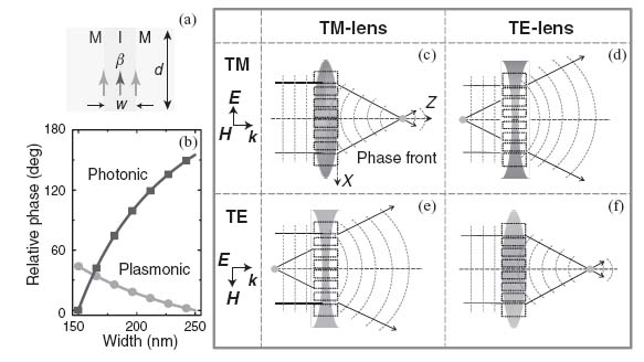
In order to design and analyze our nanoslit lenses, we considered light propagating in a slit milled through a metal film to act as a wave propagating in a metal–insulator–metal (MIM) waveguide (see Fig. 10.1a), where two different modes with distinct dispersion dependencies are possible. The first mode is a long-range SPP mode excited only with TM polarization, as only TM-polarized light can couple to the plasmonic mode. The other mode is the lowest one in the TE polarization (a photonic mode). Equations 10.1 and 10.2 show the dispersion relations calculated from a boundary value problem analysis [15] for the plasmonic and photonic modes, respectively:
FIGURE 10.1 (a) Schematic image of a MIM waveguide. (b) Relative phases plotted against the width of the gold parallel-plate waveguide for 531 nm light. The length of the waveguide, d, is 600 nm. (c–f) Schematic images of TM- and TE-lenses in TM- and TE-polarized light.
Note that  for both Equations 10.1 and 10.2. Also, w is the width of the dielectric core between the two parallel plates, β is the propagation constant,
  m and
m and  d are the permittivities of the cladding metal and the dielectric core, respectively, and k0 = 2π / λ is the wavenumber for the free-space wavelength λ. After a wave propagates through a parallel-plate waveguide for a finite distance d, the relative phase of the outgoing light is
  = arg (β d), where
  also depends on w. In Figure 10.1b, the relative phases of the outgoing light are plotted after propagating through a 600 nm long gold–polymer–gold waveguide, where the permittivity of gold is taken from Reference 16 and the polymer is polyvinylpyrrolidone (PVP) whose refractive index is 1.5. The phase of the plasmonic and photonic modes has opposite dependencies as we increase the width of the MIM waveguide so that we can design devices that will focus TM-polarized light (TM-lenses) or TE-polarized light (TE-lenses).
In a planar TM-lens, the narrowest slit is milled at the center of the lens, while wider slits are milled farther away from the center. A planar TE-lens has an opposite design: The narrowest slits are milled at the periphery of the lens, while the widest slit is milled at the center. Both lenses emulate the behavior of a conventional dielectric convex lens by modifying the phase front of light wave in a very similar manner. This happens because the wavefronts of light transmitted from the central slits are delayed relative to the wavefronts of light transmitted from the periphery slits. But when a TM-lens (TE-lens) is illuminated by TE-polarized (TM-polarized) light, the transmitted light diverges as if it were passing through a conventional dielectric concave lens. In this case, the wavefronts of light transmitted from the periphery slits are delayed relative to the wavefronts of light transmitted from the central slits. The polarization-dependent performance characteristics of both lenses are illustrated in Figures 10.1c–10.1f. The recipe for the initial design of the lens was also obtained and discussed in Reference 3.
10.2.2 Experimental Demonstration of Gold Nanoslit Lenses
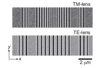
We performed optical experiments to characterize the performance of both TM- and TE-lenses. The TM- and TE-lenses were milled using a focused ion beam (FIB) into 600 nm thick gold films deposited on clean glass substrates. The SEM images of the lenses are shown in Figure 10.2. The length of each nanoslit is 22 μm, and the widths of the nanoslits vary from 69 (215) to 154 nm (163 nm) for the TM-lenses (TE-lenses). Then, a thin film of PVP was spin-coated onto the samples, filling the nanoslits to increase the contrast of the refractive indexes in the MIM slit waveguides.
FIGURE 10.2 SEM images for the TM-lens (top) and the TE-lens (bottom).
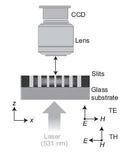
The transmission properties of the samples were measured using a conventional optical microscope with a 100X objective lens (NA = 0.75, W.D. = 0.98 mm). A schematic setup is shown in Figure 10.3. The stage resolution along the vertical direction (z-axis) and the depth of focus for the 100X objective lens are less than 1 μm, which were sufficient for our measurements. The samples were mounted on the microscope stage with the film side up and were illuminated from the substrate side with a linearly polarized, CW laser at 531 nm. The transmission images from the samples were recorded by a CCD camera by moving the height stage in increments of 1 μm. Note that the focal point of the objective lens and the surface of the sample are coincident at z = 0, and x = 0 is the center of the sample. From the obtained images, 2D maps of the transmitted light were created.
FIGURE 10.3 Schematic of the measurement setup. The distance between the lens and the sample was changed to record the irradiance at each Z position.
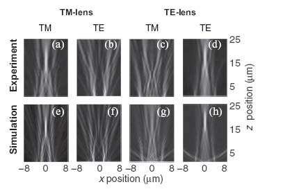
Figures 10.4a–10.4d show the transmitted light irradiance from both the TM-lens and TE-lens for both TM and TE polarizations. The TM-lens (TE-lens) focuses TM-polarized (TE-polarized) light, but diverges TE (TM) incident light. These results are a clear indication that the lenses, which were designed based on the dispersion relations above, do indeed operate as shown in Figure 10.1. The results for both lenses obtained from full-wave numerical simulations using commercial finite-element method (FEM) software (COMSOL Multiphysics) are shown in Figures 10.4e–10.4h. Considering that (i) the recorded images show the average intensity over the depth of focus of the objective lens and (ii) the two outgoing beams in Figures 10.4g and 10.4h are not observed experimentally because of the finite field of view of the objective lens, the corresponding images in Figure 10.4 are in excellent agreement with the experimental results.
FIGURE 10.4 Irradiance of the transmitted light through the nanoslit lenses. (a and b) Measurement results for the TM-lens; (c and d) measurement results for the TE-lens; (e and f) simulations for the TM-lens; (g and h) simulations for the TE-lens. Incident illumination is TM-polarized for (a), (c), (e), and (g) and TE-polarized for (b), (d), (f), and (h). In (a–h), the color scale is normalized to its maximum.
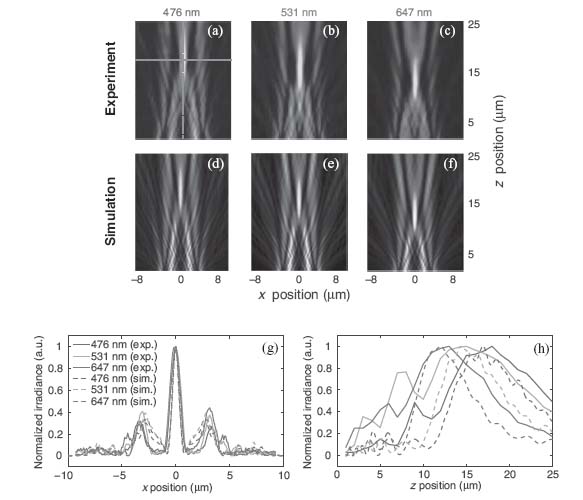
Next, we studied the wavelength-dependent properties of nanoslit lenses. Gold is dispersive, and thus chromatic aberration should exist. Since the TM-lens and the TE-lens work similarly, here we limit ourselves to the TM-lens case. In experiments, we repeated the optical measurement at wavelengths of 476 and 647 nm with TM-polarized light. In simulations, we calculated the electromagnetic field intensities in the device for wavelengths of 476 and 647 nm with the same conditions as 531 nm except for the incident wavelength. The results from the experiments and simulations are summarized in Figure 10.5. As shown in Figure 10.5, the focus distances become shorter as the incident wavelength is reduced. Figures 10.5g and 10.5h depict the cross section of the normalized irradiance at the focal plane heights and the cross section of the normalized irradiance at x = 0, respectively, proving that a good quantitative match exists between our experiments and simulations. The widths of the focal spots are wider in both the x and z directions, which could be due to imperfection of fabrication. Note that it is possible to make use of this wavelength-dependent property (i.e., chromatic aberration) as a micro spectrometer to measure the incident wavelength.
FIGURE 10.5 Wavelength-dependent irradiance of the transmitted light through the TM-lens with TM-polarized light at 467, 531, and 647 nm. (a)–(c) are from the experiments and (d)–(f) are from the FEM simulations. (g) Cross section at the focus distances for the TM-lens at each wavelength. (h) Cross sections at x = 0 μm for the TM-lens at each wavelength. In (g) and (h), each curve is normalized to its maximum; the legend for (g) applies to (h) as well.
10.3 METALLIC NANOSLIT LENSES WITH FOCAL-INTENSITY TUNEABILITY AND FOCAL LENGTH SHIFTING
The nanoslit lenses shown above are passive devices. By incorporating index-changing materials into the nanoslits, we can achieve external control over the focusing properties of the lenses. We chose LCs and a nonlinear semiconductor material as our index-tuneable materials. We then studied the focusing properties of the lenses whose slits were filled with these index-changing materials.
10.3.1 Liquid Crystal-Controlled Nanoslit Lenses
In optics, LCs are known to exhibit large refractive index changes when their orientation or phase changes [17]. Typically, the absolute value of a refractive index change is on the order of 0.1. When LCs are in the nematic phase, the orientation of the LCs can be changed by applying an electric field. Some LC materials have a phase transition temperature between the nematic and isotropic states that is close to room temperature, which makes it easy to control the phase of the LC material.
In our work, we have filled the slits of the nanoslit lenses with LCs in order to take advantage of their index-changing property. We experimentally show that the irradiance pattern changes when LCs change their phase from the nematic state to the isotropic state. These LC-controllable properties are novel features that have not been demonstrated in any previous work on metallic lenses [3, 11].
It is important to note that the purpose of using LCs in our work is to alter the transmission profiles from the nanoslit lenses, while other researchers have used LCs to shift the resonance conditions [18–23]. The LC used in our study is 5CB (4-cyano-4′-pentylbiphenyl), which has also been used in Reference 16] The nematic–isotropic phase transition temperature of 5CB is 35°C, which is close to room temperature and thus makes this LC easy to work with experimentally.
The experimental procedure is quite similar to the previous experiments except all the measurements were carried out both at room temperature (22°C, RT) and at 42°C (HT) by heating the microscope stage. More details of the experimental setup can be found in References 3 and 4.
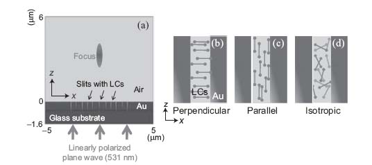
To verify our experimental results, we conducted full-wave numerical simulations using a commercial FEM software package (COMSOL Multiphysics). The geometrical parameters of the sample were taken from scanning electron microscope (SEM) images. The permittivity of gold is −12.8 + 1.12i at 531 nm [16], and the refractive index of the LCs was taken from Reference 17. When simulating for the RT case, we assumed that the LC was in the nematic state and that the LC molecules were aligned perpendicular to the sidewalls of the gold slits [18, 22]. The LC refractive index tensor was defined as n = diag(1.74, 1.55, 1.55). When simulating for the HT case, we assumed the LC to be isotropic and defined the refractive index tensor as n = diag(1.6, 1.6, 1.6). The computational domain was truncated by a scattering boundary condition, and a monochromatic plane wave was incident from the sample/substrate boundary. The geometry of the model and the orientations of the LCs are shown in Figure 10.6.
FIGURE 10.6 Simulation setting. (a) Geometry of the simulation (TM-lens) and (b–d) orientation of the LCs modeled in the simulations. The actual tapered shapes of the slits are modeled from the cross-section images of SEM.
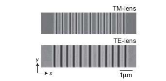
Representative SEM images of the fabricated samples are shown in Figure 10.7. Each slit is 22 μm long for both the TM- and TE-lenses. Compared to the wavelength of the illuminating light, the slits are substantially long, and we therefore assume both lenses to be essentially two-dimensional. Both lenses are symmetric with respect to the centerline or center slit. We define the origin of the coordinate at the surface of the lens at center. The x-axis is perpendicular to the slits, the y-axis is along the slit, and the z-axis is vertical to the sample.
FIGURE 10.7 SEM images for the TM-lens (top) and the TE-lens (bottom).
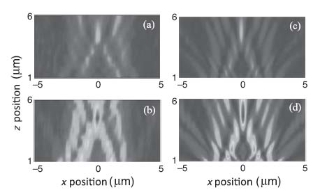
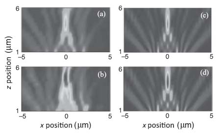
In Figure 10.8, we plot the irradiance of the transmitted light from the TM-lens. Figure 10.8a is at RT and Figure 10.8b is at HT. The color scales for both 2D plots are identical and normalized to the maximum value recorded at HT. It is clearly seen that the irradiance at HT is higher than the irradiance at RT. The observed change in irradiance can be attributed to the nematic–isotropic phase change of the LCs inside the slits. Figures 10.8c and 10.8d are the simulation results for TM-lens in the nematic state and the isotropic state, respectively. By comparing Figures 10.8c and 10.8d, it is obvious that the simulation confirms our experimental results that irradiance is higher in the isotropic state than in the nematic state. The observed changes in irradiance can be qualitatively understood by the following reasoning. Consider TM-polarized light propagating through an MIM waveguide in a plasmonic mode. With a lower permittivity in the dielectric layer, less field penetrates into the metal, and thus losses are lower in the metal layer. In our case, when the temperature of the LC rises and the LC becomes isotropic, the x-component of the permittivity decreases, which results in higher transmission.
FIGURE 10.8 Irradiance of the transmitted light through the TM-lens. (a and b) 2D plot of the experimentally measured irradiance at RT (a) and at HT (b). The color scale is normalized to the maximum of HT. (c and d) 2D plot of the numerically calculated irradiance in the nematic state (c) and in the isotropic state (d). The color scale is normalized to the maximum of the isotropic state.
In Figure 10.9, we show similar irradiance plots for the TE-lens. Figure 10.9a is at RT and Figure 10.9b is at HT. Similar to the TM-lens case, the irradiance at HT is higher than the irradiance at RT. We have also carried out numerical simulations for the TE-lens, the results of which are shown in Figures 10.9c and 10.9d. In the case of TE-polarized light (electric field in the y-direction), the light experiences a refractive index change of 0.05. Figure 10.9c is for the nematic state and Figure 10.9d is for the isotropic state. From the two 2D plots, we see that the irradiance in the nematic state is higher than the irradiance in the isotropic state, which agrees well with our experimental results. For TE-polarized light propagating through an MIM waveguide in a photonic mode, more of the field is confined to the dielectric layer. Hence when the y-component of the dielectric's permittivity increases, the result is a higher transmission throughput. Thus, heating the LCs to the isotropic state again increases the transmission in this case. The difference in the transmitted irradiance of the TE-lens at the two temperatures is smaller compared to the case of the TM-lens. This is because the relevant refractive index change in the LCs in the TE-lens case is smaller than the relevant refractive index change in the LCs for the TE-lens.
FIGURE 10.9 Irradiance of the transmitted light through the TE-lens. (a and b) 2D plot of the experimentally measured irradiance at RT (a) and at HT (b). The color scale is normalized to the maximum of HT. (c and d): 2D plot of the numerically calculated irradiance in the nematic state (c) and in the isotropic state (d). The color scale is normalized to the maximum of the isotropic state.
To gain more quantitative insight into the operation of our nanoslit lenses, we have plotted the transmitted irradiances along the z-axis in Figures 10.10a and 10.10b for the TM-lens and the TE-lens, respectively. From the experimental results for the TM-lens, the focal lengths at RT and HT are 4.0 and 4.5 μm, respectively. At HT, the irradiance at the focus is 2.7 times higher than the irradiance at the focus at RT. From the simulation results, the focal lengths in the nematic state and the isotropic state are 4.500 and 4.565 μm, respectively. The simulation results also show 2.5 times higher irradiance at the focus for the isotropic state compared to the nematic state. In looking at the experimental results from the TE-lens, we see that the focal lengths at RT and HT are identical at 4.0 μm. The irradiance at focus for the HT case is 1.3 times higher than the irradiance at focus for RT. The simulation results show that the focal lengths in the nematic and isotropic states are both 4.129 μm, while the irradiance in the isotropic state at focus is 1.2 times higher than the irradiance in the nematic state. Considering the resolution of our measurement setup and the nonuniform distribution of the LCs inside the slits, the experimental results and the simulation results are in rather good agreement.
FIGURE 10.10 Irradiance along the z-axis for the TM-lens (a) and for the TE-lens (b).
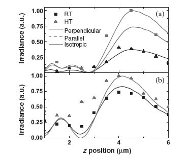
We also note that Sanda et al. have reported that the orientation of 5CB, which is the LCs studied in this paper, is parallel to the gold surface in their studies [24]. Our results can also be used to confirm the assumption of the orthogonal orientation of LC molecules relative to the wall (indicated as perpendicular in Fig. 10.6). In order to verify our assumption of the LC orientation, we also simulated a parallel LC orientation inside the slits (n = diag(1.55, 1.55, 1.74)). The results are included in Figure 10.10. In the case of the TM-lens, if the parallel orientation of the LCs is assumed for RT, the ratio of the irradiances at focus in the nematic state and the isotropic state is 1.35, which does not correspond to our experimental results. In the case of the TE-lens, the parallel orientation and the perpendicular orientation are equivalent because of the illumination polarization. Therefore, we conclude that the majority of the LC molecules inside the slits are indeed perpendicularly oriented with respect to the side walls of the gold slits in the nematic state.
10.3.2 Nonlinear Materials for Controlling Nanoslit Lenses
In this section, we numerically investigate the performance of the nanoslit lens with a nonlinear material using a recently developed and efficient FEM simulation scheme [5]. Some of the common semiconductors such as GaAs, Si, and InGaAsP are known to have high Kerr nonlinearities on the order of 10−18 m2/V2 [25]. These materials are widely used and easy to handle, and thus they are suitable choices for materials to be incorporated into our nanoslit lenses.
The simulated device is schematically shown in Figure 10.11 [26] and is conceptually similar to the nanoslit lenses above. The device is a 570 nm thick silver slab with five subwavelength slits distributed evenly from top to bottom and with identical 400 nm offsets between their centers. The sequence of slit widths is 100, 70, 60, 70, and 100 from one edge of the lens to the other. Note that the slit width sequence is symmetric about the center slit. The slits are filled with a nonlinear Kerr medium (with  l = 2.25 + i0 and χ(3) = (10−18 + i0) m2/V2), and the surround medium is air. The structure is illuminated by a plane wave with a wavelength of 850 nm moving from left to right (see Fig. 10.11) through the lens structure.
FIGURE 10.11 (a) Geometry of a nonlinear focusing device. A 570 nm thick silver film is illuminated by an 850 nm plane wave moving from left to right through five subwavelength slits (with a 100, 70, 60, 70, 100 nm slit width sequence) distributed evenly from top to bottom with 400 nm center-to-center offsets. Intensity-dependent refractive indexes at an incident field magnitude of 100 (b), 200 (c), and 350 MV/m (d). Intensity-tuneable focusing at the incident magnitude of 100 (e), 200 (f), and 350 MV/m (g).
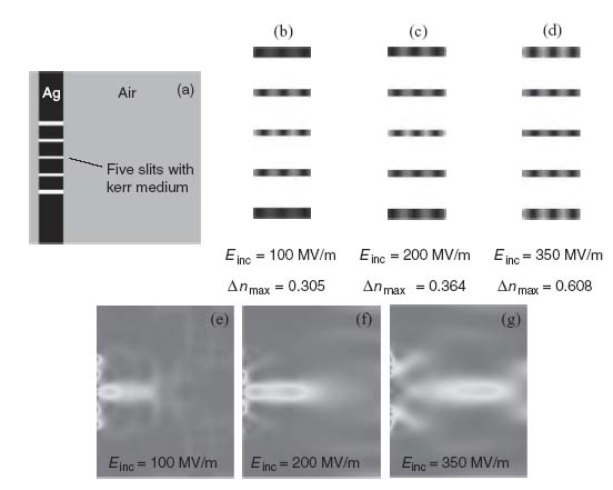
The intensity-tuneable focusing capability of this nanoslit lens enabled through the use of different SPP modes excited in the structure at different intensities of the incident light. Figure 10.11a depicts the intensity-tuneable refractive index in the slits. Figure 10.11b shows the distribution of the nonlinear part of the refractive index in the slits for an incident E-field magnitude of 100 MV/m. Here the maximum Δn = 0.305 is obtained inside the central slit, and the widest slits (the 100 nm slits at the top and bottom) are not activated at this field level. Figure 10.11b shows the evolution of this process as the incident field magnitude approaches 200 MV/m. The maximum of Δn = 0.305 is still achieved in the central slit, but the widest 100 nm slits are already moderately engaged. Finally, as the incident magnitude reaches 350 MV/m, as shown in Figure 10.11d, the maximum Δn = 0.608 is now obtained in the fully activated widest slits, while the central slit is almost deactivated.
The above process results in an intensity-tuneable focusing performance sequentially shown in Figures 10.11e–10.11g as the intensity increases from 100 to 350 MV/m. The constructive interference of the different activated slits moves the focal point further away from the device as the incident intensity increases.
10.4 LAMELLAR STRUCTURES WITH HYPERBOLIC DISPERSION ENABLE SUBWAVELENGTH FOCUSING WITH METALLIC NANOSLITS
The nanoslit lenses considered so far focus incident light in the far zone in air; hence, their spot sizes are limited by the diffraction limit. In this section we show that nanoslit lenses can go beyond the diffraction limit with the use of HMMs. A number of researchers have already studied the focusing properties and near-field distributions or SPPs in order to achieve subwavelength focusing, including the use of surface plasmon lenses [27] and a near-field plate [28]. Our work differs from those methods in that we have dealt with diffracted fields propagating away from the apertures (slits, holes, etc.).
Two exemplary structures used to design HMMs are metal–dielectric lamellar composites and metallic nanowires. Between these two structures, planar multilayer structures are easier to fabricate in samples with sub-micrometer thicknesses, and hence we have chosen a metal–dielectric multilayer structure for our work. When the layer thicknesses of the metal and dielectric materials are much smaller than the free-space wavelength, the effective permittivity of the multilayer structures is calculated by effective medium theory (EMT) [29]. Depending on the signs of  x and
x and  z, HMMs can be classified into two groups: transverse positive (TP,
  x > 0,
  z < 0) and transverse negative (TN,
  x < 0,
  z > 0). In the visible region, it is easy to find metals and dielectrics for a TN-HMM. Metals could be low-loss noble metals such as silver or gold, and the dielectric could be silica, alumina, or titanium dioxide. On the other hand, finding materials to obtain a TP-HMM in the optical region is not trivial as noble metals have a negative permittivity that is too large, while the indexes of dielectrics are on the order of unity. One combination could be titanium nitride (TiN) for the metal and aluminum nitride (AlN) for the dielectric [30]. Forming a planar multilayer structure with thick dielectric layers and ultrathin metal layers [31] is yet another option.
To begin our analysis, we consider a single nanoslit lens with an HMM-covered substrate, where diffracted large-wavenumber waves (high-k waves) are allowed to propagate inside the HMM slab [2]. The propagation direction of high-k waves in an HMM with negligible losses is approximated as
where θ is the angle from the normal axis,  = (Sx, Sz) is the Poynting vector, and
  = diag(
 x,
x,  z) is the permittivity of the HMM. After careful optimization of a given double-slit design and choosing appropriate materials for the actual planar lamellar metal–dielectric composite comprising the HMM, the diffracted high-k waves could form a desired interference field pattern with subwavelength features [2]. When the design is adjusted such that the maximum field of the pattern occurs at the interface of the HMM and the substrate, the device could work as a subwavelength probe.
One significant drawback of a passive optical HMM is that the intrinsic loss in the metal always limits the overall functionality [32, 33]. This is a fundamental challenge in the applications of HMMs, but it can be overcome by including active (gain) media in the system [34–36]. So far, gain media have been experimentally incorporated into various kinds of plasmonic and metamaterial systems including SPPs [37], localized SPPs [38], plasmonic waveguides [39], and negative index materials [35]. Incorporating gain within the multilayer system allows for the compensation of the metallic loss [40]. In fact, some experiments on metamaterials have even shown complete loss compensation or even overcompensation [35]. With gain, then, metal–dielectric HMM applications can be far more robust than with passive HMMs. This section starts with the modeling of a metal–dielectric HMM for the case when the dielectric is an active medium, and we study the dispersion relationship of such a system. Then, we numerically study the subwavelength diffraction properties of the double slits with the active HMM. As a preliminary demonstration, we show our experimental results on subwavelength diffraction patterns where the HMM is passive.
10.4.1 Active Lamellar Structures with Hyperbolic Dispersion
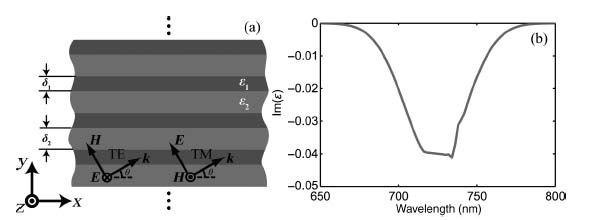
The cross section of a binary HMM, which consists of isotropic metal and dielectric layers, is schematically shown in Figure 10.12a. The permittivity and thickness of each layer are denoted respectively as  j and δj, where j = 1 for the metal layer and j = 2 for the dielectric layer, and the period of the structure is δ = δ1 + δ2. We also define a linearly polarized plane wave with the following free-space parameters: wavelength λ, wavenumber k0 = 2π/λ, and wavevector k0 = k0 (
 cos θ +
  sin θ), where a given angle of incidence θ is aligned with the structure (0 < θ < π / 2). As discussed above, HMMs made from thin, alternating layers of a metal and a dielectric can be considered to be metamaterials as long as their periodicity δ is significantly smaller than λ or, more precisely, when k0 δ
  1.
1.
FIGURE 10.12 (a) Geometry of a metal–dielectric multilayer composite. The permittivities of the metal and dielectric layers are denoted, respectively, as  1 and
1 and  2, and the thicknesses are δ1 and δ2. All the layers are parallel to the x–z plane. (b) Extracted imaginary part of the dielectric function of dye-doped epoxy. Note that the real part of the dielectric function (not shown) is dominated by the permittivity of the epoxy, which is about 2.72.
We consider four different methods to analyze the dispersion relation of the HMM design above. When studying the dispersion relationships of multilayers, using T-matrices to form a set of nonlinear equations (NLE) is a rigorous method, and the resulting solutions are exact [41]. A simpler way is to use the standard EMT (denoted as EMT1 here). The EMT homogenizes the multilayers, thus giving the effective dielectric constants of the medium as a whole. A more advanced EMT method (denoted EMT2) [42] takes into account the nonlocal effects that are neglected in EMT1. With regard to numerical methods, spatial harmonic analysis (SHA) is a robust method to study periodic systems [43, 44]. All the details of the four methods discussed here are given in the addendum of Reference 6.
We have estimated the properties of metal–dielectric multilayers using the four methods mentioned above. We take silver as the material in all the metal layers. Note that thin silver films tend to form islands below 20 nm on a silica surface, which is not suitable for obtaining a multilayer structure. Recent studies have shown that a silver film evaporated on a 1 nm thick germanium layer is continuous and smooth even at a 5 nm Ag thickness [31]. In our calculations, we used realistic values of the optical properties of the materials; these values are taken from experimental results. We take the permittivity of silver from Reference 45, which uses a Drude–Lorentz model with three Lorentz terms. The parameters are fitted using measured data from Reference 16. The loss factor (a multiple of the collision rate in the Drude term) is set to 2 in order to take into account the size-dependent sliver loss [31]. Since annealing can reduce the loss of germanium to negligible levels in the red part of the spectrum, which is our region of interest, the germanium layer is not modeled in our simulations. For the active dielectric medium, we take the gain values extracted from experimentally measured data of an organic dye (Rh800) mixed in epoxy [35, 46]. Typically, organic dyes mixed with polymers have high gain coefficients and have the advantage that they can be incorporated into any arbitrarily shaped spaces [35]. The refractive index of epoxy is 1.65, and the emission peak of Rh800 occurs at about 720 nm. Because the gain coefficient of a material is proportional to the imaginary part of the refractive index, we modeled the active dielectric with a complex dielectric function. The imaginary part of the dielectric function is plotted in Figure 10.12b. Note that the real part of the dielectric function is not plotted here since it is dominated by the permittivity of the epoxy and is almost constant in this wavelength range. To simplify our modeling, we assumed that the active medium was operating in the saturated regime, and hence we neglected the time dependence of the gain saturation.
As an example of an experimentally feasible system, we take a silver–gain multilayer structure consisting of alternating 20 nm thick silver layers and 40 nm thick gain layers. In Figure 10.13, we plot the effective anisotropic permittivity of the structure calculated from the four methods (EMT1, EMT2, NLE, and SHA). The incidence angle (θ) is zero for the plot. Within the plotted wavelength range (650–800 nm), all four methods show that the multilayer has opposite signs for  x and
x and  y, and the system therefore exhibits hyperbolic dispersion.
FIGURE 10.13 Wavelength dependence of the effective anisotropic permittivity for the silver–gain HMM at normal incidence (θ = 0) calculated from EMT1 (dashed-dotted line), EMT2 (dashed line), NLE (solid line), and SHA (dotted line). Top left panel: the real part of the effective permittivity. Top right: the imaginary part of the effective permittivity. Bottom panels: relative errors in percent with respect to the SHA results. Note that the results from NLE and SHA are coincident, and their curves therefore overlap completely. The real part of permittivity in the y-direction from EMT2 overlaps with the NLE and SHA curves (therefore it is obscured by the NLE and SHA curves and is not seen in the figure), and the rest of the EMT2 curve partially overlaps with the NLE and SHA curves.
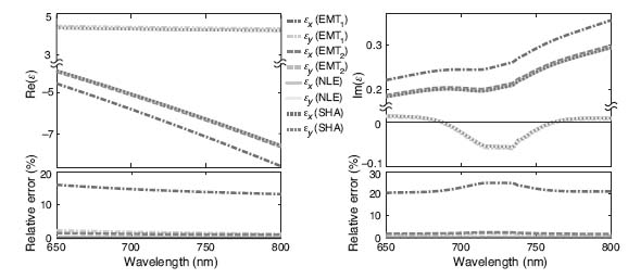
Figure 10.13 also shows that the effective permittivities resulting from NLE and SHA are perfectly matched in both the x- and y-directions. This is not surprising, as both methods are aimed at calculating the eigenvalues of the composite layer and differ only in their numerical realizations. The results from EMT2 are very close to those values. However, there are significant discrepancies between the results from EMT1 and those from the other methods. The relative errors are calculated using the results from SHA as the reference (exact value) using | ( calc –
  SHA)/
SHA)/ SHA| × 100%. Comparing with EMT1, EMT2 is more accurate and has lower error over the calculated wavelength range (the EMT2 error is less than 3% in this case). We also note that the relative errors of the imaginary parts of the permittivities from both EMT1 and EMT2 are higher in the active region, which can be observed from the relative error plots in Figure 10.13.
If we take a look at the fundamental mode for a TM-polarized wave propagating in the x direction in the structure, the real part of the modal index, which is  , is higher than the refractive index of the dielectric in the multilayer. This indicates that the dominant propagating mode is indeed a plasmonic mode. The imaginary part of the modal index, which has the same sign as Im(
 y), is negative from 700 to 750 nm. Within this range, the propagating TM wave is loss-free. However, in the x direction, we can see that the imaginary part of
  x stays positive, which means that the loss is not compensated for a TE-polarized wave inside the structure. It is important to point out that although the loss is not fully compensated in the x direction, it is still lower than it would be without gain. To achieve loss compensation in both directions in this type of bilayer metamaterial, we need an enormously large gain coefficient. It is also worth mentioning that the actual loss might be lower in real structures because the active medium within the metal–dielectric multilayer structure will give rise to an effective gain that is much higher than its bulk counterpart. The large value of gain is due to the local-field enhancement inherent in the plasmonic response of the structure [35].
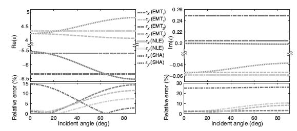
In Figure 10.14, we plot the incidence-angle-dependent dispersion relationship of the silver–gain HMM. The incident wavelength is 720 nm. Here again we see perfect agreement between the NLE and SHA results. The results from EMT1 do not show any dependence on the angle of incidence. The EMT2 results show that this method can only handle angle-dependent problems in the y-direction, and it has nonnegligible error compared to the NLE or SHA results. As shown in Figure 10.14, the permittivities in the x- and y-directions both show variations on the order of 1 in this case, which are rather strong changes. Thus, we should use either NLE or SHA to take into account the angular dependence of the permittivity if we are dealing with angles away from normal incidence.
FIGURE 10.14 Incidence-angle dependence of the effective anisotropic permittivity for the silver–gain HMM at a wavelength of 720 nm calculated from EMT1 (dashed-dotted line), EMT2 (dashed line), NLE (solid line), and SHA (dotted line). Top left panel: real part of the effective permittivity. Top right: imaginary part of the effective permittivity. Bottom panels: relative errors in percent with respect to the SHA results. Note that the results from NLE and SHA are coincident, and their curves overlap.
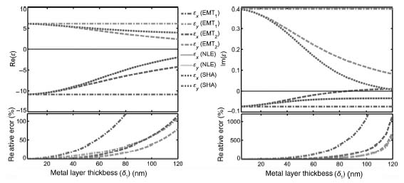
Our studies included an analysis of how the effective permittivity changes when varying the thicknesses of the metal layers. Figure 10.15 shows the calculated effective anisotropic permittivities when the metal–layer thickness was varied from 5 to 120 nm. The metal volume fraction was kept constant at 0.5 (i.e., δ1 = δ2). From the plotted curves, we can see that the results from NLE and SHA again show perfect agreement. The EMT1 method does not have any thickness dependence at all, which could also be concluded from its formula. This method shows a significant amount of error when the metal–layer thickness is large. For instance, when the metal thickness reaches 60 nm (corresponding to a period of 120 nm, i.e., λ/6), the relative error for EMT1 is greater than 50%. The EMT2 method behaves slightly better, but the error also becomes nonnegligible when the thickness increases.
FIGURE 10.15 Effective anisotropic permittivity for the silver–gain HMM with different metal-layer thicknesses at a wavelength of 720 nm at normal incidence (θ = 0) calculated from EMT1 (dashed-dotted line), EMT2 (dashed line), NLE (solid line), and SHA (dotted line). The volume fraction of the metal layer (δ1/δ) is kept constant at 0.5. Top left panel: real part of the effective permittivity. Top right: imaginary part of the effective permittivity. Bottom panels: relative errors in percent with respect to the SHA results. Note that the results from NLE and SHA are coincident, and their curves overlap.
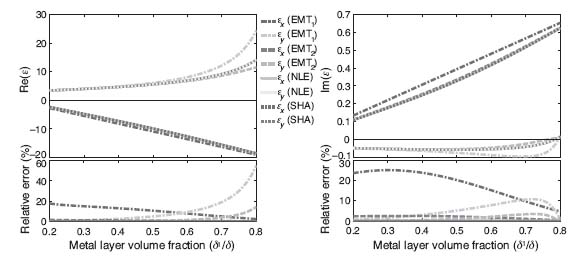
We also investigated the calculated effective permittivity as a function of the metal volume fraction (δ1/δ). The period (δ) was kept constant at 60 nm in this case, and the results are shown in Figure 10.16. As before, we again see that the NLE and SHA results match perfectly. For EMT1 and EMT2, the results show that, in the x direction, the error increases as the metal volume fraction decreases. In the y-direction, however, we see the opposite trend. We observe that, depending on the application, EMT1 can produce substantial errors in both the x- and y-directions of the effective dielectric function. The EMT2 calculation gives more accurate results for major applications. The NLE and SHA methods are the most accurate for all the cases.
FIGURE 10.16 Effective anisotropic permittivity for the silver–gain HMM with different metal volume fractions at a wavelength of 720 nm at normal incidence (θ = 0) calculated from EMT1 (dashed-dotted line), EMT2 (dashed line), NLE (solid line), and SHA (dotted line). The period (δ) is kept constant at 60 nm. Top left panel: real part of the effective permittivity. Top right: imaginary part of the effective permittivity. Bottom panels: relative errors in percent with respect to the SHA results. Note that the results from NLE and SHA are coincident, and their curves overlap.
10.4.2 Subwavelength Focusing with Active Lamellar Structures
In this section, we numerically explore the effect of loss compensation with an active HMM [6]. The structure contains a Cr mask layer that is 50 nm thick with two 40 nm wide slits separated by 250 nm (see Fig. 10.17a). The HMM structure consists of 10 layers of alternating 5 nm thick silver layers and 16 nm thick dye-doped epoxy layers. This kind of structure is only possible if an ultrathin germanium layer is used as a wetting layer for each layer [31], and multilayer formation requires a repetition of deposition and spin-coating [47]. The dye used in the simulation is Rh800 whose maximum emission wavelength is at 716 nm, and the parameters are taken from Reference 35. There is a 16 nm thick dye-doped epoxy layer between the chromium slit structure and the first layer of silver; this epoxy material also fills the slits as well. The substrate is assumed to be pure epoxy (not doped with dye).
FIGURE 10.17 (a) Schematic diagram for a double-slit design with silver–dye multilayer structure. (b) Normalized irradiance at the interface between the silver–dye HMM and the epoxy substrate calculated with gain (solid line) and without gain (dashed line). The arrow in (a) shows the position of the interface.
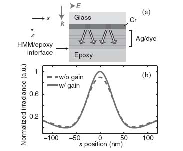
In our simulations, we assumed that the dye was fully saturated when plotting the active (gain) case. In comparison, we also simulated the case without gain in which the epoxy was not doped with dye. At a wavelength of 716 nm, the components of effective permittivity with gain and without gain were about ( x,
x,  z) = (− 10.71 + 0.41i, 6.14 + 0.026i) and (
 x,
x,  z) = (− 10.71 + 0.39i, 6.14 − 0.073i), respectively. The simulated full-width at half-maximums (FWHMs) of the diffraction patterns at the interface of the multilayer structure and the substrate are shown in Figure 10.17b. With gain, the FWHM of the irradiance at the interface was about 47 nm, which is about λ/15. If the structure contained no gain, the irradiance at the interface was reduced, and the FWHM of the field intensity increased to about 54 nm as indicated by the dashed line in the figure.
10.4.3 Experimental Demonstration of Subwavelength Diffraction
In this section, we present and discuss our experimental results on subwavelength diffraction with a nanoslit device. Our device consists of two metallic slits of subwavelength width placed on top of a planar, lamellar structure of alternating metal and dielectric layers. A photolithography approach is employed to provide subwavelength detection. Our experiments show that light diffracted from a double slit into an HMM indeed can form a subwavelength pattern in photoresist, which is in contrast to double-slit diffraction into an ordinary, isotropic medium.
In our experimental design, we chose silver and silica for the binary lamellar structure. Such a structure has low losses in the blue spectral range. The effective permittivity of our HMM made of equally thick silver and silica layers was calculated from an EMT analysis [29]. The permittivities of silver and silica were obtained with spectroscopic ellipsometry. The imaginary part of the permittivity of silver was found to be 1.7 times larger than the literature value [16]. Hence, the effective permittivity tensor at 465 nm is diag( x,
x,  z) = diag(− 2.78 + 0.22i, 6.31 + 0.15i), and the isofrequency curve is a hyperbola. Using Equation 10.3, the propagation direction in our silver–silica HMM is about 34°. Such an oblique beaming angle is preferable to obtain an interference pattern in the HMM. Note that for hyperlens designs [48, 49], the propagation direction was almost normal to the interface.
In order to fabricate the double slit with an HMM slab, we first deposited a 50 nm thick chromium film on a glass substrate using an electron-beam evaporator. Then, using FIB milling (Nova 200, FEI), the double-slit design was milled into the chromium film. A schematic diagram and an SEM image of the double slit are shown in Figures 10.18a and 10.18b, respectively. The separation of the two slits was 270 nm, and the width of each slit was 50 nm. In order to fill the slits, we spin-coated diluted poly(methyl methacrylate) (PMMA) on the chromium film. The PMMA solution was prepared by further diluting 950PMMA A4 (MicroChem Corp.) with anisole in a 1:4 volume ratio. This gives a final film thickness of 18 nm after spin-coating at 3000 rpm for 40 s and a soft bake at 185°C for 5 min on a hotplate. On top of the PMMA layer, we deposited three pairs of alternating silver and silica layers for a total of six 15 nm thick layers. To have smooth and continuous silver films, 1 nm thick germanium layers were deposited before each of the silver layers [31]. Hence, the final structure looks like the images shown in Figure 10.18c, and the total thickness of the multilayer structure including the PMMA layer was 111 nm. We also prepared a control sample consisting of a single 110 nm thick layer of silica instead of the alternating metal–dielectric layers (see Fig. 10.18f).
FIGURE 10.18 Schematic diagram (a) and a SEM image (b) of the double slit milled in a chromium film. Schematic diagram of the double slit with a silver–silica lamellar HMM slab (c) and a photoresist layer spin-coated on a glass substrate (d). Schematic diagram of the double slit with a silver–silica lamellar HMM slab in contact with a photoresist layer (e) and the double slit with a reference silica slab in contact with a photoresist layer (f) illuminated by TM-polarized light. Incident and diffracted fields are shown in red, and the dips created after exposure are illustrated. AFM images after development for the silver–silica lamellar HMM sample (g) and the silica-layer sample (h). The dimensions of the images in the x-axis are 600 and 1000 nm for (g) and (h), respectively.
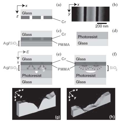
We used the double-slit HMM samples to expose positive photoresist films (AZ 1518, AZ Electronic Materials) in order to detect the diffraction pattern. The photoresist was spin-coated on a glass substrate (see Fig. 10.18d). The light source used for exposing the photoresist was a linearly polarized Ar/Kr CW laser (43 Series, Melles Griot) operating at a wavelength of 465 nm. When exposing the sample, the photoresist was brought into contact with the sample, and the sample was illuminated from the Cr film side in the TM polarization as shown in Figures 10.18e and 10.18f. The subwavelength slits can be assumed to be line sources (or point sources in a 2D cross section), and the arrows in Figures 10.18e and 10.18f schematically show the light propagation in each structure. As discussed earlier, light propagation inside an HMM is expected to be directional, while light in a dielectric will propagate in all directions.
After exposure, the photoresist was developed with AZ developer (AZ Electronic Materials) for 1 min. The dip created by the photolithography exposure process was scanned by atomic force microscope (AFM, Veeco Dimension 3100 with a high aspect ratio tip Veeco Nanoprobe Tip TESP-HAR). The AFM scans of the exposed and developed photoresist layers on the silver–silica lamellar HMM sample and the reference silica-layer sample are shown in Figure 10.18g and 10.18h, respectively. It is clear that the dip created by the HMM sample is much narrower compared to the dip created by the reference silica sample. This is due to the fact that the high-k waves propagating in the HMM structure are recovered at the photoresist, leading to a narrower exposed dip in the PMMA. For the reference silica sample, however, the high-k waves are lost because they are evanescent in the isotropic silica material, and hence the exposed area is larger since only lower-k waves are recovered at the PMMA interface.
To verify our experimental results on the diffraction of high-k waves inside the HMM and to optimize the performance of the double-slit/HMM device, we have conducted full-wave FEM simulations using COMSOL Multiphysics with all dimensions taken from the fabricated samples. The permittivities of the materials were extracted from spectroscopic ellipsometry measurements. The computational domain was truncated by scattering boundary conditions, and a 465 nm TM-polarized plane wave (electric field polarized across the slits, see Fig. 10.18e) was incident from the top boundary. To directly compare with our experimental results, the control structure with a single silica layer was simulated as well. The irradiance of the transmitted light for the silver–silica lamellar HMM and the silica reference slabs is shown in Figures 10.19a and 10.19b, respectively. While the silica slab creates a diffraction-limited pattern, the HMM directs the diffracted light into a subwavelength-scale spot at the HMM–substrate interface, due to the directional propagation of high-k waves from the slits. Note that the HMM pattern is still “diffraction limited” but this limit is much lower for the hyperbolic media.
FIGURE 10.19 Simulated irradiance through a double-slit structure at a wavelength of 465 nm into a silver–silica lamellar HMM slab with 15 nm thick layers of silver and silica (a) and in a single layer of silica (b). The structures in (a) and (b) correspond to the experimentally fabricated samples. (c) Same as (a) but with 2 nm thick layers of silver and silica and 28 pairs of layers. (d) A semi-infinite silver–silica HMM slab with 2 nm layer thicknesses. The color scales in (a), (c), and (d) are normalized to each panel's peak diffraction irradiance, and the color scale in (b) is same as in (a).
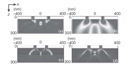
For our HMM structure with a relatively large structural period, the limitations of the EMT approximation become significant [6, 50]. One of the indications of that issue is the beam walk-off parallel to the layer interfaces that we observe in the simulations (Fig. 10.19a). We would expect some changes in the results when we decrease the period of the HMM structure while leaving the effective parameters formally the same. To investigate this scenario, we simulated a hypothetical HMM structure consisting of 28 pairs of silver and silica layer with 2 nm layer thicknesses. The total thickness of the HMM was 112 nm, which is approximately the same as the experimental sample thickness. In this case the distance between the two slits was set to 200 nm to maximize the irradiance at the center. The calculated irradiance is shown in Figure 10.19c. Since this structure has a smaller period, its performance is closer to the homogeneous effective medium case. Compared to Figure 10.19a, we see more distinct beaming in Figure 10.19c. In terms of the beam propagation angle, the angles in Figures 10.19a and 10.19c are 51° and 40°, respectively. The structure in Figure 10.19c gives a propagation angle that is closer to the angle obtained from Equation 10.3. What is more important is that the pattern size is significantly decreased, as shown below. We have also plotted a semi-infinite slab of alternating 2 nm thick silver/silica layers. These results, plotted in Figure 10.19d, depict the interference of two ideally symmetric diffraction patterns obtained from each slit. Figure 10.19c, in contrast, illustrates additional interference with the backscattered field, which destroys the symmetry of the individual diffraction patterns. These modeling and simulation efforts were actually performed before the experiments, and the initial EMT-based estimates have been followed by full-wave modeling to optimize the distance between the slits that would maximize the center peak intensity.
In Figure 10.20a, we show the AFM scans averaged along the slits for the silver–silica lamellar HMM sample exposed for 8–10 min. When the pattern depth in photoresist is 15 nm, the FWHM of the dip was 83 nm. Longer exposure times resulted in a deeper profile and a wider FWHM. Thus for exposure depths of 35 and 42 nm, the FWHM values are 105 and 135 nm, respectively. The depth of the exposure does not increase, but the FWHM continues to increase above a certain exposure time that depends on the resist extinction and the irradiance. Our results clearly indicate that planar metal–dielectric lamellar structures have the capability to transform the diffracted light from the slits into a subwavelength interference spot. In Figure 10.20b, we show the normalized AFM scans presented in Figure 10.20a as well as those of the silica-layer sample. As the penetration depth (exposure time) increases, the contrast improves and the FWHM increases. If we were to extrapolate the experimental profile to even smaller depths, the side lobe peaks would grow and the central peak would be narrower. The overall depth profile would approach that of the simulated irradiance just near the resist surface.
FIGURE 10.20 (a) Depth profiles from the AFM scans for the silver–silica lamellar HMM sample with three different depths depending on the exposure conditions. (b) Normalized depth profiles of the HMM sample shown in (a) and the silica-layer reference sample. (c) Simulated irradiances at the slab–substrate interface for the lamellar HMM slab (Ag/SiO2) and the uniform slab of silica.
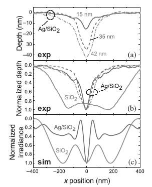
Figure 10.20c depicts the irradiances at the interfaces of the layer(s) and the substrate obtained from the simulations shown in Figure 10.19. The FWHMs of the central peaks of the HMM structure and the single silica layer are 45 and 514 nm, respectively, which agree well with our experimental results. When comparing the experimental results and the simulations, we need to keep in mind that the tightest spot occurs at the interface photoresist and the final silica layer for the HMM sample. As the distance from the interface increases, the peak-to-background ratio becomes worse. This happens because the photoresist is not a hyperbolic medium, and therefore the waves entering the photoresist from the multilayers diverge within a few tens of nanometers. Since the depth of the dip is 15 nm even for the shallowest result, it is natural that the FWHM of the experimentally measured dip is wider than that from the simulation results of Figure 10.20c. The overall picture approaches the simulated results if the depth of the dip is shallower. The simulations for the 28-layer structure show potential for improving the resolution. Indeed, the FWHM of the interference peak for this short-period structure is only about 22 nm. However, to reach this resolution, the photoresist quality should be improved. The best available resist at our wavelength has grains of about 60 nm, which limits the attainable resolution [51].
10.5 SUMMARY
We have shown that arrays of nanoslits could exhibit unique features with the aid of plasmonics and metamaterials. By taking advantage of the width-dependent phase of light exiting the slits, we have designed lenses to focus either TM-polarized or TE-polarized light. These same lenses act as concave lenses for the orthogonal polarization of incident light. The fabricated lens prototypes were studied experimentally, and the results were successfully corroborated by numerical simulations. Similar types of lenses could exhibit tuneability in their focal intensities as well as their focal lengths when the slits are filled with index-changing materials.
We have also shown that nanoslits with HMMs work as subwavelength focusing devices. The dispersions of active HMMs were investigated by four different methods, and our analysis showed loss compensation in one of the permittivity components. We have considered practical designs for the devices and have numerically shown that the active HMM can generate a more intense and smaller focus, as small as λ/15. We observed a λ/6 diffraction peak from our fabricated sample with a passive HMM. Devices such as these could work as subwavelength probes, and the planar and compact design is beneficial for various applications including lithography and sensing.
ACKNOWLEDGMENTS
This work was supported in part by the United States Army Research Office (ARO) Multidisciplinary University Research Initiative (MURI) program award 50342-PH-MUR; ARO grants W911NF-04-1-4070350, W911NF-09-1-0075, W911NF-09-1-0231, and W911NF-09-1-0539; and National Science Foundation (NSF) Partnerships for Research and Education in Materials grant DMR 0611430. Support was also provided by Samsung Advanced Institute of Technology, United States Office of Naval Research (ONR) MURI grant N00014-10-1-0942, US Air Force Office of Scientific Research (AFOSR) grant FA9550-10-1-0264, Intelligence Community Postdoctoral Research Fellowship grant 104796, and NSF-DMR 1120923. AVK and VPD would also like to cite partial support by US Air Force Research Labs (AFRL) Materials and Manufacturing Directorate – Applied Metamaterials Program.
REFERENCES
1. Cai W, Shalaev V (2009) Optical Metamaterials: Fundamentals and Applications. Springer-Verlag.
2. Thongrattanasiri S, Podolskiy VA (2009) Hypergratings: nanophotonics in planar anisotropic metamaterials. Opt. Lett. 34: 890–892.
3. Ishii S, Kildishev AV, Shalaev VM, Chen KP, Drachev VP (2011) Metal nanoslit lenses with polarization-selective design. Opt. Lett. 36: 451–453.
4. Ishii S, Kildishev AV, Shalaev VM, Drachev VP (2011) Controlling the wave focal structure of metallic nanoslit lenses with liquid crystals, Laser Phys. Lett. 8: 828–832.
5. Kildishev AV, Litchinitser NM (2010) Efficient simulation of non-linear effects in 2D optical nanostructures to TM waves. Opt. Commun. 283: 1628–1632.
6. Ni X, Ishii S, Thoreson MD, Shalaev VM, Han S, Lee S, Kildishev AV (2011) Loss-compensated and active hyperbolic metamaterials. Opt. Express 19: 25255–25262.
7. Ishii S, Kildishev AV, Drachev VP (2012) Diffractive nanoslit lenses for subwavelength focusing. Opt. Commun., 285: 3368–3372.
8. Ishii S, Kildishev AV, Narimanov E, Shalaev VM, Drachev VP (2013) Subwavelength diffraction pattern from a double-slit in hyperbolic media, Laser Photonics Rev. 7: 265–271.
9. Sun Z, Kim HK (2004) Refractive transmission of light and beam shaping with metallic nano-optic lenses. Appl. Phys. Lett. 85: 642–644.
10. Shi H, Wang C, Du C, Luo X, Dong X, Gao H (2005) Beam manipulating by metallic nano-slits with variant widths. Opt. Express 13: 6815–6820.
11. Verslegers L, Catrysse PB, Yu Z, White JS, Barnard ES, Brongersma ML, Fan S (2009) Planar lenses based on nanoscale slit arrays in a metallic film. Nano Lett. 9: 235–238.
12. Lin L, Goh XM, McGuinness LP, Roberts A (2010) Plasmonic lenses formed by two-dimensional nanometric cross-shaped aperture arrays for Fresnel-region focusing. Nano Lett. 10: 1936–1940.
13. Huang FM, Zheludev N, Chen Y, de Abajo FJG (2007) Focusing of light by a nanohole array. Appl. Phys. Lett. 90: 091119.
14. Huang FM, Kao TS, Fedotov VA, Chen Y, Zheludev NI (2008) Nanohole array as a lens. Nano Lett. 8: 2469–2472.
15. Kim KY, Cho YK, Tae HS, Lee JH (2006) Light transmission along dispersive plasmonic gap and its subwavelength guidance characteristics. Opt. Express 14: 320–330.
16. Johnson PB, Christy RW (1972) Optical constants of the noble metals. Phys. Rev. B 6: 4370–4379.
17. Khoo IC, Wu ST (1993) Optics and Nonlinear Optics of Liquid Crystals. Vol. 1. World Scientific.
18. Kossyrev PA, Yin A, Cloutier SG, Cardimona DA, Huang D, Alsing PM, Xu JM (2005) Electric field tuning of plasmonic response of nanodot array in liquid crystal matrix. Nano Lett. 5: 1978–1981.
19. Chu K, Chao C, Chen Y, Wu Y, Chen C (2006) Electrically controlled surface plasmon resonance frequency of gold nanorods. Appl. Phys. Lett. 89: 103107.
20. Evans P, Wurtz G, Hendren W, Atkinson R, Dickson W, Zayats A, Pollard R (2007) Electrically switchable nonreciprocal transmission of plasmonic nanorods with liquid crystal. Appl. Phys. Lett. 91: 043101.
21. Dickson W, Wurtz GA, Evans PR, Pollard RJ, Zayats AV (2008) Electronically controlled surface plasmon dispersion and optical transmission through metallic hole arrays using liquid crystal. Nano Lett. 8: 281–286.
22. Berthelot J, Bouhelier A, Huang C, Margueritat J, Colas-des-Francs G, Finot E, Weeber J-C, Dereux A, Kostcheev S, Ahrach HIE, Baudrion A-L, Plain J, Bachelot R, Royer P, Wiederrecht GP (2009) Tuning of an optical dimer nanoantenna by electrically controlling its load impedance. Nano Lett. 9: 3914–3921.
23. Xiao S, Chettiar UK, Kildishev AV, Drachev V, Khoo I, Shalaev VM (2009) Tuneable magnetic response of metamaterials. Appl. Phys. Lett. 95: 033115.
24. Sanda PN, Dove DB, Ong HL, Jansen SA, Hoffmann R (1989) Role of surface bonding on liquid-crystal alignment at metal surfaces. Phys. Rev. A 39: 2653–2658.
25. Boyd RW (2003) Nonlinear Optics. Academic.
26. Min C, Wang P, Jiao X, Deng Y, Ming H (2007) Beam manipulating by metallic nano-optic lens containing nonlinear media. Opt. Express 15: 9541–9546.
27. Srituravanich W, Fang N, Sun C, Luo Q, Zhang X (2004) Plasmonic nanolithography. Nano Lett. 4: 1085–1088.
28. Merlin R (2007) Radiationless electromagnetic interference: evanescent-field lenses and perfect focusing. Science 317: 927.
29. Rytov SM (1956) Electromagnetic properties of a finely stratified medium. Sov. Phys. JETP 2: 466–475.
30. Naik GV, Schroeder JL, Sands TD, Boltasseva A (2011) Titanium nitride as a plasmonic material for visible wavelengths. Arxiv preprint. arXiv: 1011.4896.
31. Chen W, Thoreson MD, Ishii S, Kildishev AV, Shalaev VM (2010) Ultra-thin ultra-smooth and low-loss silver films on a germanium wetting layer. Opt. Express 18: 5124–5134.
32. West P, Ishii S, Naik G, Emani N, Shalaev VM, Boltasseva A (2009) Searching for better plasmonic materials. Laser Photonics Rev. 4: 765–808.
33. Bloemer MJ, D'Aguanno G, Scalora M, Mattiucci N, de Ceglia D (2008) Energy considerations for a superlens based on metal/dielectric multilayers. Opt. Express 16: 19342–19353.
34. Zhang J, Jiang H, Gralak B, Enoch S, Tayeb G, Lequime M (2009) Compensation of loss to approach-1 effective index by gain in metal-dielectric stacks. Eur. Phys. J. Appl. Phys. 46: 32603.
35. Xiao S, Drachev VP, Kildishev AV, Ni X, Chettiar UK, Yuan HK, Shalaev VM (2010) Loss-free and active optical negative-index metamaterials. Nature 466: 735–738.
36. Andresen MPH, Skaldebo AV, Haakestad MW, Krogstad HE, Skaar J (2010) Effect of gain saturation in a gain compensated perfect lens. J. Opt. Soc. Am. B 27: 1610–1616.
37. Seidel J, Grafström S, Eng L (2005) Stimulated emission of surface plasmons at the interface between a silver film and an optically pumped dye solution. Phys. Rev. Lett. 94: 177401.
38. Noginov MA, Zhu G, Bahoura M, Adegoke J, Small CE, Ritzo BA, Drachev VP, Shalaev VM (2006) Enhancement of surface plasmons in an Ag aggregate by optical gain in a dielectric medium. Opt. Lett. 31: 3022–3024.
39. De Leon I, Berini P (2010) Amplification of long-range surface plasmons by a dipolar gain medium. Nat. Photonics 4: 382–387.
40. Tumkur T, Zhu G, Black P, Barnakov YA, Bonner CE, Noginov MA (2011) Control of spontaneous emission with functionalized multilayered hyperbolic metamaterials. Proc. SPIE 8093: 80930O.
41. Yeh P (2005) Optical Waves in Layered Media. 2nd ed. Wiley Series in Pure and Applied Optics. Wiley-Interscience. p 416.
42. Elser J, Podolskiy VA, Salakhutdinov I, Avrutsky I (2007) Nonlocal effects in effective-medium response of nanolayered metamaterials. Appl. Phys. Lett. 90: 191109.
43. Ni X, Liu Z, Boltasseva A, Kildishev AV (2010) The validation of the parallel three-dimensional solver for analysis of optical plasmonic bi-periodic multilayer nanostructures. Appl. Phys. A 100: 365–374.
44. Liu Z, Chen KP, Ni X, Drachev VP, Shalaev VM, Kildishev AV (2010) Experimental verification of two-dimensional spatial harmonic analysis at oblique light incidence. J. Opt. Soc. Am. B 27: 2465–2470.
45. Ni X, Liu Z, Kildishev AV (2010), “PhotonicsDB: Optical Constants” https://nanohub.org/resources/PhotonicsDB. (DOI 10.4231/D3FT8DJ4J).
46. Sivan Y, Xiao SM, Chettiar UK, Kildishev AV, Shalaev VM (2009) Frequency-domain simulations of a negative-index material with embedded gain. Opt. Express 17: 24060–24074.
47. Tumkur T, Zhu G, Black P, Barnakov YA, Bonner CE, Noginov MA (2011) Control of spontaneous emission in a volume of functionalized hyperbolic metamaterial. Appl. Phys. Lett. 99: 151115.
48. Jacob Z, Alekseyev LV, Narimanov E (2006) Optical hyperlens: far-field imaging beyond the diffraction limit. Opt. Express 14: 8247–8256.
49. Salandrino A, Engheta N (2006) Far-field subdiffraction optical microscopy using metamaterial crystals: theory and simulations. Phys. Rev. B 74: 075103.
50. Wood B, Pendry J, Tsai D (2006) Directed subwavelength imaging using a layered metal-dielectric system. Phys Rev. B 74: 115116.
51. Melville DOS, Blaikie RJ (2005) Super-resolution imaging through a planar silver layer. Opt. Express 13: 2127–2134.


