4
Experimental Methods
The two preceding chapters illustrate important characteristics about the framework in which experiments to be designed and executed. The vast majority of XAFS measurements are carried out on storage ring sources via applications for a limited amount of beam time. Generally there is no guarantee of a second chance should the experiments fail due to user error; the starting position of assessors will be: “Why didn’t you do it right the first time?” Almost equally serious is not having sufficient beam time to complete the project. At best, this might mean a delay of 6 months in completion of a research paper or thesis. Accordingly, pre‐planning of an experiment at the proposal stage is of high importance. This should have a scope covering:
- Obviously, why is this scientifically more interesting than competing proposals?
- Does the experiment match the characteristics of the source?
- Do the facilities at the beamline accord with your needs?
- Will any experimentation of your own gel with the space, control systems, and safety requirements of the facility?
- Which absorption edges will you study? Can the beamline be easily configured for any changes that are in mind?
- What is the best way of presenting the samples for your experiment? How long might each measurement take?
- Do you need to record XAFS spectra of a set of reference materials to aid your analysis?
- Including a modicum of contingency, what is the total time required to complete this experiment?
- Is this viable given the staffing that you can provide at the experiment?
A careful analysis of this, with discussions with the beamline staff, will increase the probability of success with applications as well as experimental execution. Experiments are broadly in two classes: technique development and scientific applications. Defining the beam time for the former can be more difficult, and require more contingency. But the majority of applications are of the latter type when the majority of time is expended on creating the sample state and carrying out measurements on the resulting materials.
4.1 Sample Characteristics
4.1.1 X‐Ray Absorption of Samples
The absorption properties of the samples are often the most important, and least considered, aspect of experimental design. Here, we amplify what was outlined in Sections 2.1 and 3.5. The key formulae are reproduced here, relating the x‐ray transmission before (I0) and after (It) the sample, the linear absorption coefficient (μ), the path length of the beam through the sample (l), mass absorption coefficient (μm), and density (ρ). For composite samples, absorbance μ(E) at an energy E is the weighted sum of the components.

The attenuation length (λ) of a sample is the path length at which the x‐ray transmission drops to 1/e of the incoming value, where e is the mathematical constant and is of value ca. 2.71828, and occurs at:

The attenuation length is a useful guideline for considering sample absorption as it represents a transmission of about 37%. In practice it is advisable where possible to keep the background absorption below a value for μ(E) of 1 (i.e., at most 10% of the light may reach the detector after the sample), which will occur at ~2λ.
The attenuation of air is a fundamental factor in atmospheric design. From Figure 4.1, it can be seen that this only passes above 2.5 cm (an inch being a reasonable rule of thumb!) at ~2.4 keV, near the energy sulfur K edge. It is clear that air absorption should be avoided up to these energies. By the calcium K edge (4 keV) the attenuation length increases to ~1 dm and so small air gaps between beam pipe, sample and detectors can be accommodated. Only at ~8 keV (Ni K edge) does air absorption reach a value that might be neglected.
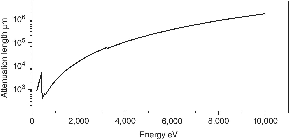
Figure 4.1 Attenuation length of dry air as a function of energy (250–10,000 eV).
4.1.2 Classes of Experimental Layouts
The most challenging experiments to set up are in the soft or low‐energy x‐ray region. As can be seen from Figure 4.1, photon energies below 2.5 keV (S K edge) are increasingly likely to be compromised by any significant air path between the components of the beamline and also with the sample cell. Generally, measurements are carried out with the sample in vacuo, ideally on a windowless beamline, that is, one with no window between the electron beam and the sample. Differential pumping is used to minimize the risk to the storage ring vacuum, but contamination in the vacuum vessel is to be avoided. Thus most soft x‐ray XAFS measurements are carried out on involatile materials mounted on a manipulator allowing several samples to be studied before venting the sample chamber. Volatile samples or in situ studies can be carried out in custom made cells with appropriate windows, often polyimides with good physical and chemical stability. Figure 4.2 presents the x‐ray transmission of a typical, thin film (25 µm of a polyimide). At the P K edge (2146 eV) such a film will transmit about 30% and thus from this energy point the window does not present a serious difficulty. A more severe problem is encountered at the Mg K edge (1303 eV), where the window transmission will be reduced to 0.009. In situ studies at lower energies will require either extremely thin carbon windows or carefully designed windowless cells with a thin layer reagent above the surface of interest.
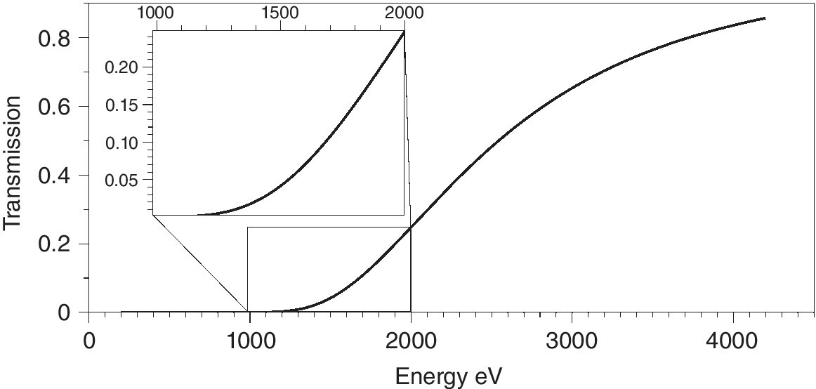
Figure 4.2 Transmission of a polyimide film (25 µm) between 200 and 4200 eV.
In the medium‐energy x‐ray region (~4 to ~10 keV) the constraints of air absorption lessen very significantly and thus a laboratory‐style spectroscopic experiment can be laid out on an experimental station. Window materials composed of light elements (e.g., plastics, boron nitride, carbon) can be used throughout. Thin windows of second row elements (Al, quartz) become viable, and, as exemplified in Chapter 6, the nature of the material under study itself sets the optimum for sample presentation. In the hard or high‐energy x‐ray region (>10 keV), these constraints lessen further and there is great flexibility for experimental design.
4.2 Scanning Modes
4.2.1 Scanning XAFS
The normal mode of recording a XAFS spectrum involves moving the Bragg angle of the monochromator from high to lower angle in a stepwise fashion, using a system outlined in Section 3.3.2 and illustrated in Figure 3.4. There may be a dwell time at that angle to allow resetting of optics and positioning prior to the acquisition time at that energy. The scan range and interval may be set either in angle (millidegrees) or, by means of an encoder on the beamline, directly into energy (eV). From equation 3.10 and a Si(111) monochromator (d = 3.1356 Å) the relationship between angle and energy can be written as in equation 4.4.
A simple stepwise acquisition with a set interval and acquisition time is satisfactory for short test or edge scans, but it is not the most efficient procedure for recording EXAFS or carrying out kinetic studies. A full EXAFS spectrum can be split into three regions (Figure 4.3). The pre‐edge region is acquired to provide a reliable baseline for background subtraction and thus can be acquired with a relatively large interval (5–10 eV) over enough energy range (200–300 eV) to provide a good extrapolation across the EXAFS spectrum and a relatively short acquisition time per point. The edge region requires a much finer step interval (~0.25 eV), generally to ensure that natural line‐width of the XANES and pre‐edge features are not distorted by the digitization interval. These features are relatively sharp and intense and so the acquisition time per point need not be increased very substantially, unless there are weak pre‐edge features. The third region is generally analyzed as EXAFS in k space, from about k = 3 Å−1 (~34 eV above E0) until the end of the recorded range (~12 to ~20 Å−1). The square relationship between (E−E0) and k (equation 4.5), means that keeping a constant interval in k (~0.025 Å−1) can be achieved with an increasing energy interval.
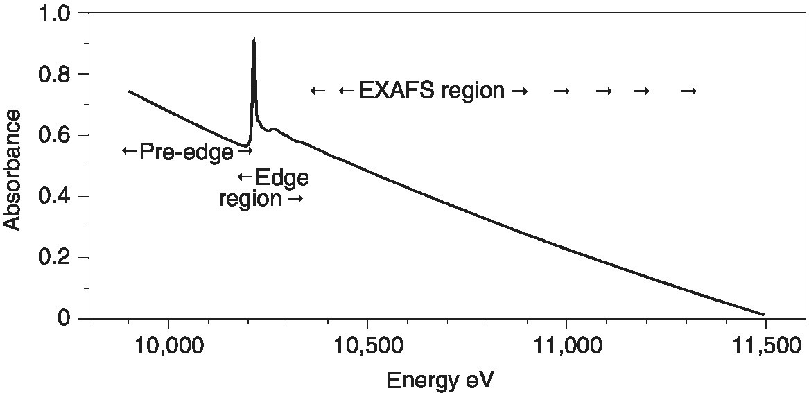
Figure 4.3 Regions of a XAFS spectrum, shown for the W L3 edge of (NBu4)2[W6O19] in CH3CN solution.
(Source: Diamond, B18, data from Richard Ilsley)
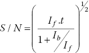
But offsetting this is the dampening of χ(k) with increasing k. EXAFS analysis is generally on data with a k weighting kn.χ(k), where n = 1, 2, or 3. Given ideal statistics, the signal to noise ratio (S/N) improves as the square root of the acquisition time (t) (equation 4.6), retrieving the S/N over a the EXAFS data range with k1 weighting would of itself require the acquisition time to have a weighting of k2. Hence the acquisition time per data point should also increase across the spectrum. Ideally this should be smoothly using a kn weighting (n ~3), but if that algorithm is not available it can be approximated by dividing the EXAFS range of the spectrum into regions with increasing energy interval and acquisition time per point.
This mode is appropriate for long scans on dilute materials when the acquisition time is considerably longer than the dwell time and thus the duty cycle is very efficient (i.e., a low dead time between points). An alternative method for spectra that can be usefully recorded more quickly is the Quick EXAFS mode (QEXAFS). In that the monochromator is driven at a constant velocity and data is acquired on the fly. This can be effected in both forward and backward directions. There is then no dwell time and so the acquisition duty cycle is extremely efficient. Care must be taken to check the calibration of both forward and reverse scans, which may show a hysteresis effect. However, this mode has been successfully enacted on many facilities providing a scan time of the order of seconds. In its most rapid mode, where the oscillation of the monochromator crystal is achieved using an eccentric cam system, XANES spectra have been successfully acquired in 25 ms, and EXAFS in under 1 second.[1]
4.2.2 Energy Dispersive XAFS
In this arrangement, one crystal is used to select x‐ray energies in a horizontal, deflecting plane, but the bandwidth is increased by bending the crystal to provide a spread of Bragg angles. The effect of this is to focus the x‐ray beam on the sample and then disperse the x‐ray bandwidth onto a multi‐element linear detector (Figure 4.4). Generally a Bragg monochromator is used and the crystal bent to a curvature that will provide XANES and EXAFS at one absorption edge, although neighboring edges can also be measured simultaneously.
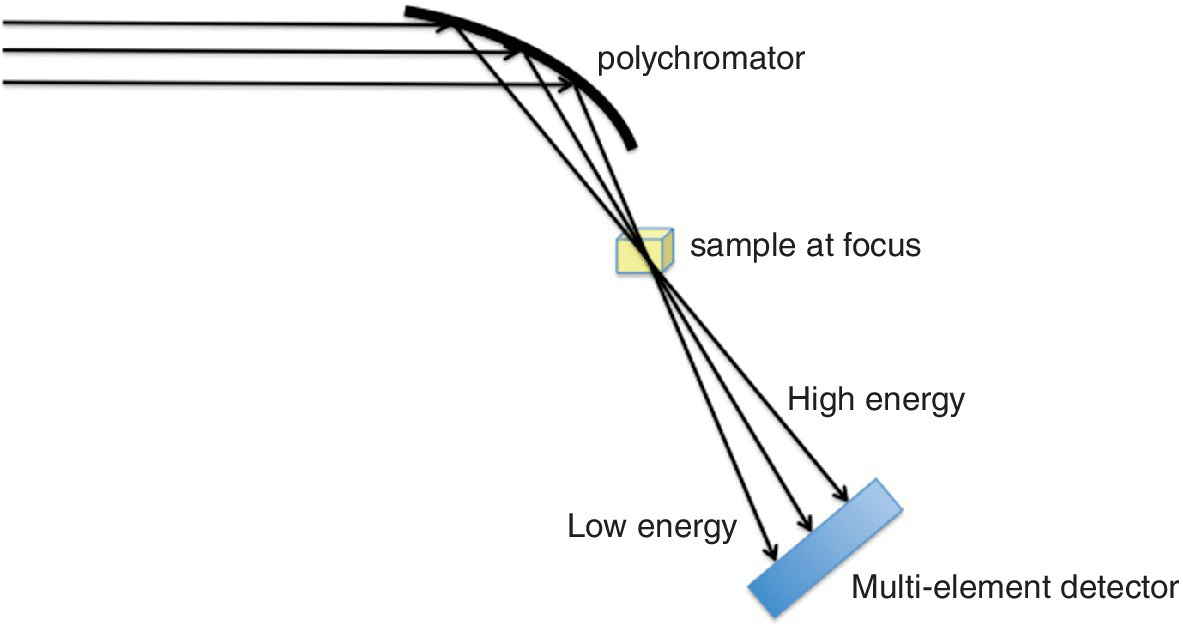
Figure 4.4 Schematic representation of energy dispersive XAFS using a Bragg monochromator.
The main advantage of the dispersive configuration is that of multiplexing. The acquisition time will be similar to that of a single energy point in a scanning spectrometer, which can be less than 1 ms. However, the technique is very demanding on x‐ray beam stability, especially since the background spectrum, I0, is not acquired synchronously, as is the case in a scanning spectrometer. Its applications tend to be situations where small beam‐size and rapid scan times are essential, such as in kinetic studies, samples at high‐pressure experiments in diamond anvil cells, and in sample mapping.[2]
4.3 Detection Methods
4.3.1 Transmission
This is the standard reference method of detecting x‐ray absorption directly. Detectors placed before and after the sample provide a relative absorbance. They need to have the properties of high resilience to x‐radiation, high sensitivity, and excellent linearity. Ion chambers are commonly used. The absorption of the device can be tuned by varying the pressures of the inert gases in the chamber. Typically the first ion chamber (I0) should have sufficient absorption (~10 to ~40%) to provide a strong signal but allow the majority of the light to pass through to the sample. The second chamber (It) has a more absorbing mix (~80 to ~95%) leaving the residue to pass through to a reference sample, typically an appropriate metal foil, with a third ion chamber (Ir) downstream of it. In this way the second and third ion chambers provide the signals for the spectrum of the reference material (Figure 4.5a). The ion chamber (Figure 4.5b) has parallel plates with a high potential difference and acts as an integrating device with no energy resolution. The voltage (~300 V) is set so that the cations from the ionized gas and the electrons travel to the collector plate rather than recombine and the current generated is linear with the x‐ray flux. At higher voltages the electrons generated can also ionize the gas and the characteristics of the chamber change from a highly linear converter of photon flux to current, through a non‐linear regime, to a proportional counter where the electron multiplication effect creates avalanches. In the ionization chamber region, the ion current, Iion, is given by equation 4.7, showing the proportionality to the photon flux absorbed in the ion chamber (N) and also to the photon energy (Eph). There is a degree of amplification from ratio of the photon energy with that required to create the electron‐ion pair.
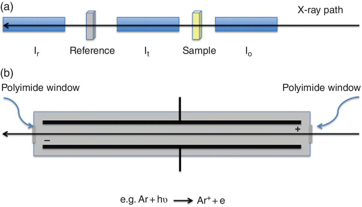
Figure 4.5 a) A configuration for measuring XAFS spectra in transmission and b) the components of an ion chamber.
For argon Egas = 26 eV, and as a result each photon of energy Eph = 10 keV will create 385 electron‐ion pairs. Figure 4.6 presents the absorption efficiency of four gases often used in ion chambers, calculated for a 0.5 bar pressure and a 10 cm path length. It is evident that argon and krypton can be used to provide absorption efficiencies over these energy ranges by varying the partial pressures. Helium may be employed as essentially a relatively transparent filler gas; nitrogen is a viable ionizable gas in the soft x‐ray region. However, as well as limitations in the applied voltage, there are also problems created by the high photon fluxes created by insertion devices on third‐generation sources. The maximum count rate is in the order of 1011phs−1cm−3. Reducing the absorption by having first row elements in the ion chamber is one approach to offsetting this problem; not only does it reduce the absorption coefficient of the gases, it also tends to increase Egas (36 and 41 eV for nitrogen and helium, respectively).
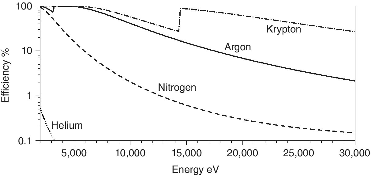
Figure 4.6 The absorption efficiency of a 10 cm path length of He, N2, Ar, and Kr at 380 torr pressure (2–30 keV).
The alternatives to ion chambers are principally thin semiconductor devices operating in a current mode. X‐radiation creates a hole‐electron pair, which requires much less energy than the current‐forming process in an ion chamber (e.g., 3.6 eV in silicon), thus the current yield per photon is higher (2780 at Eph = 10 keV). Doping of an intrinsic (i) semiconductor like silicon, with a Group 15 element, P, As, or Sb, results in an extra electron in the conduction band per dopant atom and is thus termed n‐type (negative); the corresponding effect with a Group 13 element (B, Al, or Ga) creates holes in the valence band and is termed p‐type (positive). A p‐n junction, as in most photovoltaic cells, results in a space‐charge region whereby there is a flow of electrons from the n material to the p side thus reducing the number of conductors in a depletion layer formed at the junction. This depletion layer can, in effect, be expanded by adding a sandwiched layer of the intrinsic semiconductor in what is known as a pin diode. The effect of the reverse bias voltage on a diode is shown in Figure 4.7. Starting from a p‐n junction, the diffusion of electrons to create the depletion layer causes a bend in the energy levels of the valence and conduction and bands. The potential gradient is increased with a reverse potential and this can be set to minimize the capacitance of the diode, indicating the depletion region is at a maximum and the single/background can be optimized.
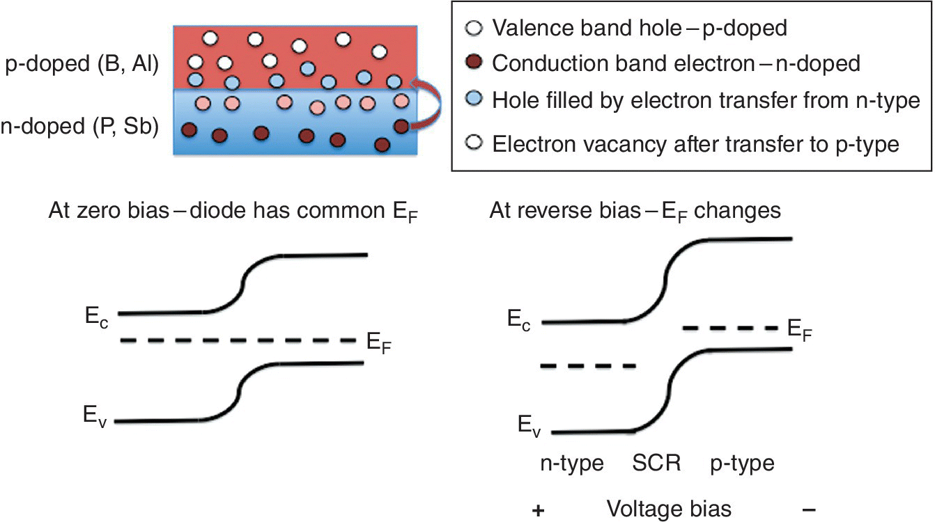
Figure 4.7 Formation of a depletion layer in a pn junction of silicon‐based semiconductors and the effect on the energies of the top of the valence band (Ev), the Fermi level, and the bottom of the conduction band (Ec) due to electron diffusion and a reverse voltage.
However, the absorption properties of the photodiode are set by the material and its thickness. As can be seen from Figure 4.8, thin diodes (<10 µm) are needed for measurement of I0 at low energies. A crystalline diode in that position will also generate diffraction and this will reduce the intensity of the through beam, creating sharp glitches in the apparent I0 value. Generally, this will exacerbate normalization of the spectrum, especially for dilute and/or inhomogeneous samples. Saturation at high count‐rates and flux densities can also be problematical. An alternative is to place a photodiode off the light path so as to intercept a small fraction of the straight‐through beam scattered off a foil or even from air, but this will reduce sensitivity.
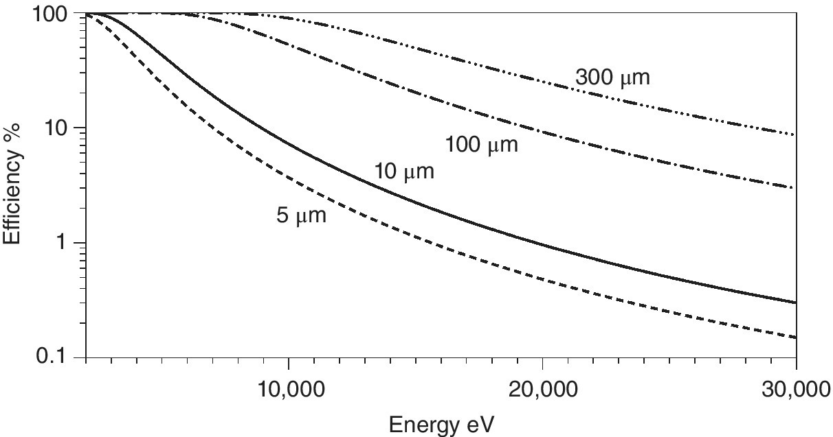
Figure 4.8 Absorption efficiency of silicon at different thicknesses (2–30 keV).
The sample itself has much to do with the quality of the spectrum recorded. In general, the absorption should be sufficiently large to give a significant change in the transmitted x‐ray intensity (It). However, if the absorption is too high then there are too few photons reaching the detector and a high noise level will ensue. If a front ion chamber (I0) is set to absorb 20% of the incident light (close to the optimum), and the sample has an absorbance (μ.l) of 1, then from equation 4.1, we can calculate the flux reaching the second ion chamber (It). If the second ion chamber is set to absorb 90% of the incident beam, then its sensitivity will be 4.5‐fold higher. As a result we can plot the relative signal intensity on It/I0 (Figure 4.9a). Clearly a μ value >5, which transmits <0.6% of the x‐rays incident on the sample, will compromise the signal intensity on the second ion chamber very considerably. On the other hand, a very small change in absorbance with Δμ <0.01 will cause a change in It of <1% and again be non‐optimum. In transmission mode the signal/noise ratio generally improves in way that is close to the information theory relationship, that is, to the square root of number of photon counts √Nph. Accordingly, the relative S/N can be estimated (Figure 4.9b). This shows an optimum range between 2 and 3 units, corresponding to a transmission through the sample of between 4 and 5%.
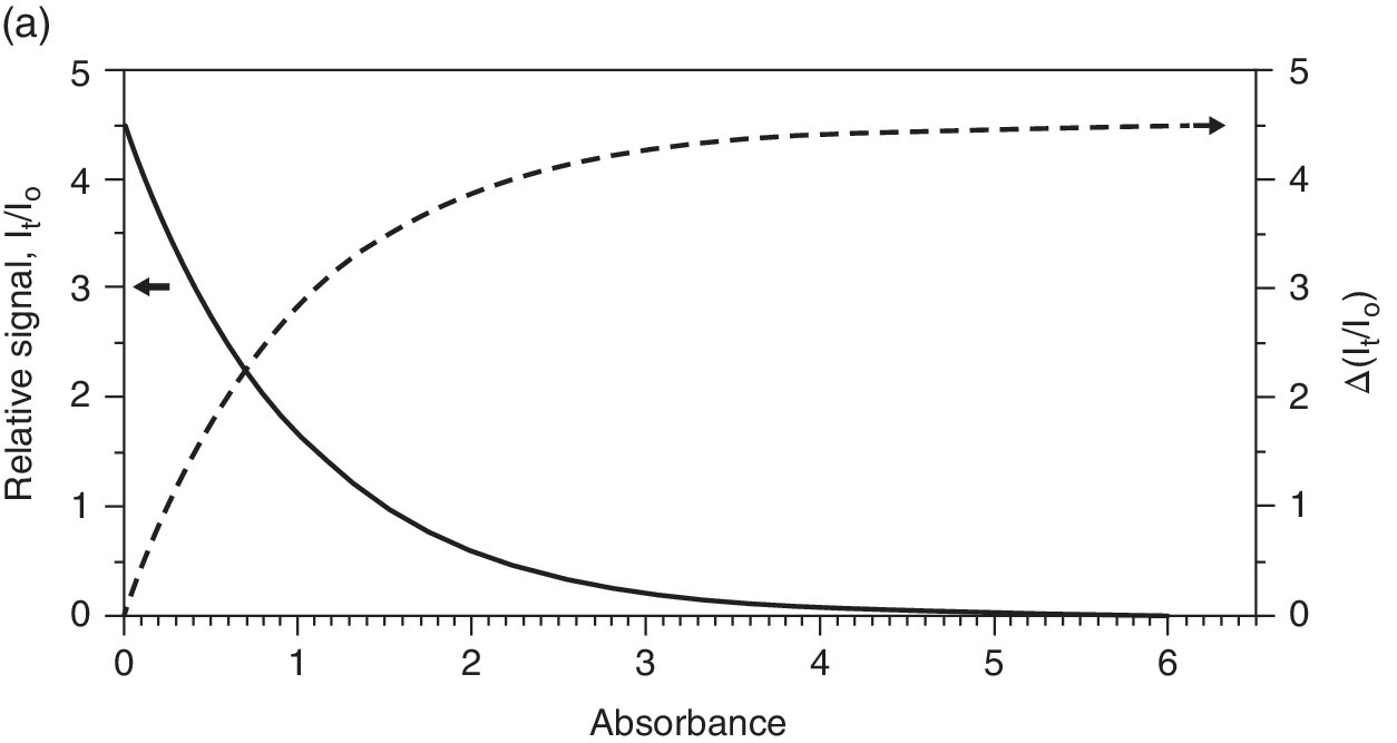
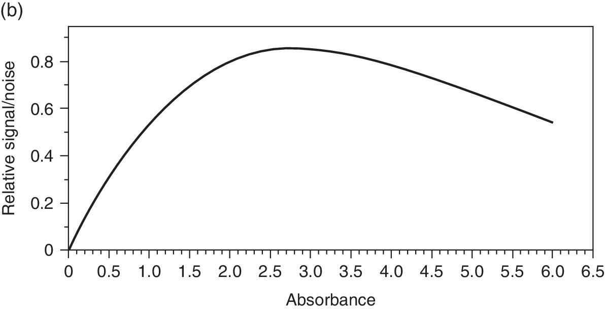
Figure 4.9 a) Relative signal intensity on It and I0 ion chambers as a function of sample absorbance, μ, if 90% and 20% absorbing, respectively. b) Relative signal/noise (S/N) versus sample absorbance.
The sample thickness to achieve this varies with the chemical composition of the material, its density and the absorption edge energy (Figure 4.10). Taking twice the attenuation length (2λ) as a rule of thumb, then a uniform film should be created, which will vary from about 8 µm for the sulfate to 140 µm for molybdate. This is not trivial starting from typical powdered samples, and errors in sample presentation can result in distorted relative intensities. A danger is that an inhomogeneous sample is presented to the x‐ray beam, with variable sample thicknesses (Figure 4.11). As shown in Figure 4.12, the result of this can be an increase in the transmission to the second ion chamber. The additional light, however, is not passing through the sample and contains no information about it. Hence the XAFS features will have an inaccurate intensity profile. Since these types of samples are often used for model structures, the risk is that this error is transferred to other solid samples or to solutions. Additional risks from inhomogeneous samples are that sample settling, and beam movement can vary the quantity of sample that is with the x‐ray beam during the recording of the spectrum.
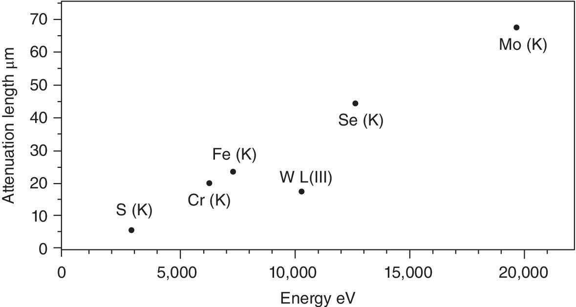
Figure 4.10 Attenuation length (µm) at 50 eV above the absorption edges of compounds of formula Na2EO4 at normal density (E = S, Cr, Fe, W, Se, and Mo).
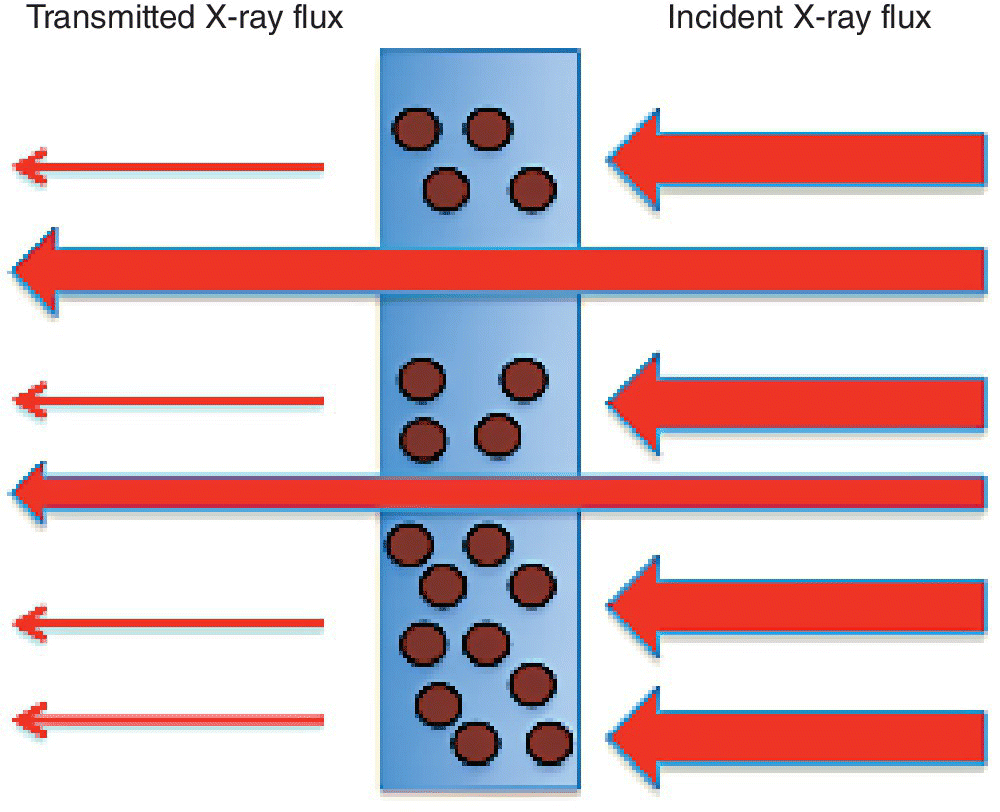
Figure 4.11 Effect of pinholes on the x‐ray transmission through a solid sample.
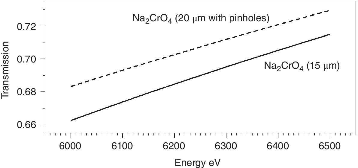
Figure 4.12 Comparison of the transmission of a sample of Na2CrO4 above the Cr K edge (ignoring EXAFS features) for a sample with a uniform thickness (15 µm) packed at a density of 1.4 gcm−3 with one of 20 µm thickness with 25% of the sample area containing pin holes.
Solutions provide an excellent means of presenting a homogeneous sample and thus circumventing this problem. However, the starting points of many analyses are the reported crystal structures of model compounds. The normal means of approaching solution‐type homogeneity with a true solid sample is to use a diluent and create a finely divided physical mixture, by, for example, mortar and pestle grinding or ball‐milling. The diluent would generally be an inert, low atomic number material such as boron nitride, cellulose, or synthetic polymer powders. They may then be either laid into a sample holder of known thickness, or, more often, pressed into a pellet. If this is carried out in a glove box with a dried diluent, and the sample sealed between windows, then the technique can be applied to air‐sensitive materials.
We can consider Na2CrO4 as an example for optimizing sample preparation. From equation 2.2 (v.s.), the quantity of Na2CrO4 (MW 166) required to give an absorption of 2 at a point sufficiently above the edge to be near a normalization level (50 eV, i.e., 6040 eV photon energy) can be determined from equation 4.8.
Hence mass/area needed = 2/196.4 g/cm2 = 10.2 mg/cm2
The edge jump that would result from this sample can be calculated from the mass absorption coefficients below (63 cm2/g) and after (519 cm2/g) the edge. The mass weighted increase in the absorption coefficient is then 153.9 cm2/g Na2CrO4, which, on this density of sample, would give an edge jump of ~1.6. The diluent and the sample thickness can be varied to ensure that this density of material is presented homogeneously to the beam. This combination of total absorption (2) and edge jump (1.6) should provide the basis of recording a high‐quality spectrum; this should also be the case if the sample density were 50% higher than this. Generally, transmission should be the method of first choice, as it will in most cases give the best S/N and reliable spectrum. Indeed, recording in transmission has become viable to ever lower sample concentrations as sources become brighter and optics and detectors uprated; the threshold varies greatly with photon energy, with higher energies more favorable, and also with sample type (favoring lighter non‐absorbing elements in the sample matrix). However, there are samples where transmission is not viable, and indirect measurement of absorption must be employed.
The effective sensitivity of transmission XAFS depends upon both upon the sampling depth and the intrinsic absorption change at an edge. Plots of the attenuation lengths for edges of elements from P to Po, and energies below 30 keV, are given in Figure 4.13 for solutions of 50 mM in aqueous solutions. Clearly for the higher edge energies, the greatly increased potential path length can improve sensitivity, providing there is sufficient sample for the attendant volume increase.
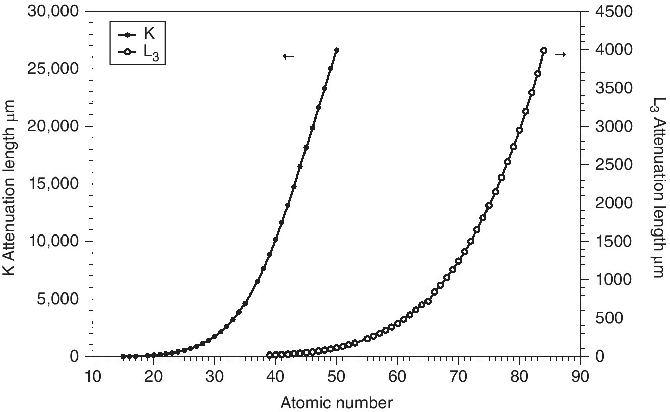
Figure 4.13 Attenuation length of aqueous solutions (50 mM) of elements (P –Po) at the onset of their K and L3 absorption edges of energy less than 30 keV.
The resulting changes in sample absorption (edge jumps) at the sample attenuation length (Figure 4.14a) show the expected increases with atomic number. But it is also apparent that the relative slopes differ from those of the plots of attenuation length (Figure 4.13). Indeed, when this is normalized to the same path length (Figure 4.14b), it can be seen that the intrinsic sensitivity decreases with atomic number. It is also evident that the sensitivity of the L3 edges is higher than that of the deeper‐lying K edges; this is important for thin samples. Ultimately though, as sensitivity is pressed, the absorbance change of EXAFS oscillations in particular is too small compared to the discrimination of the detection system. In that situation, indirect methods may provide increased signal/background by virtue of having very low background signals.
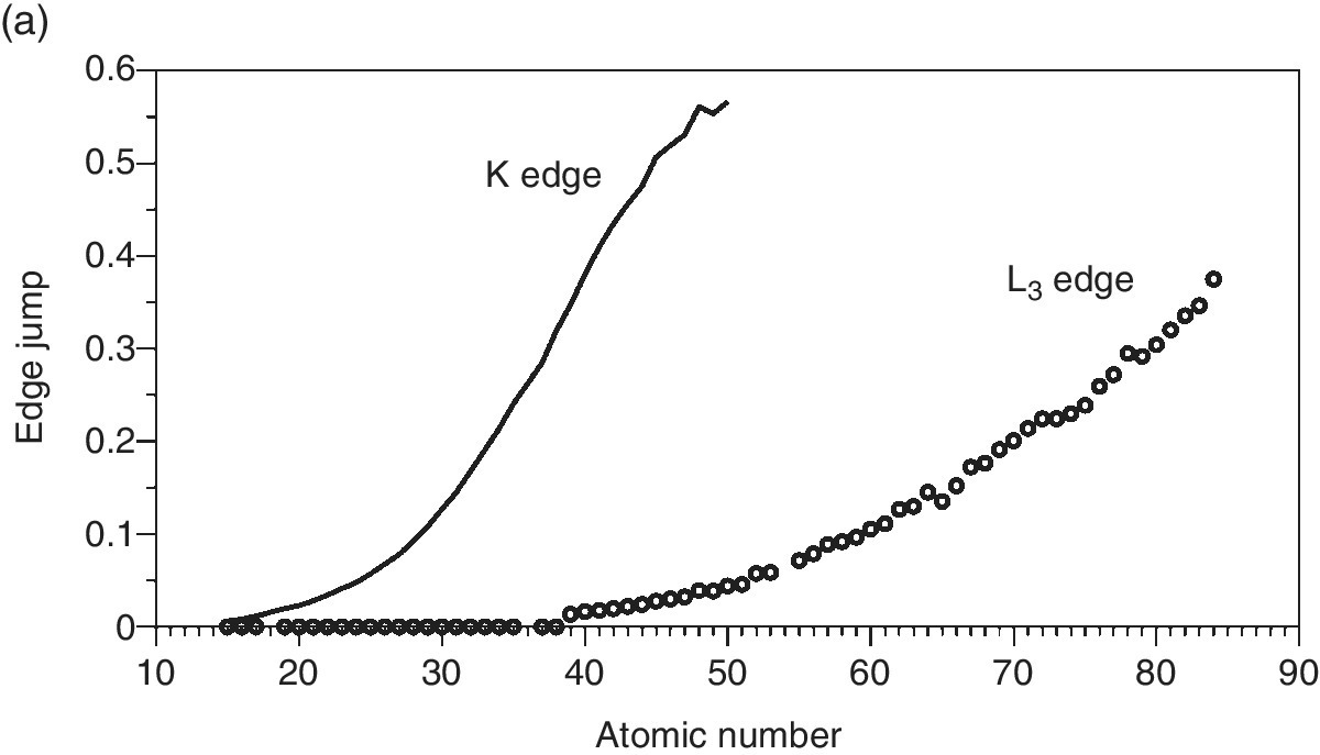
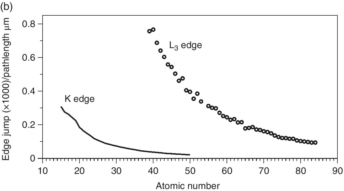
Figure 4.14 The change is x‐ray absorbance of aqueous solutions (50 mM) of elements (P–Po) at their K and L3 absorption edges of energy less than 30 keV. a) for a sample thickness of the attenuation length and b) per µm pathlength.
4.3.2 Electron Yield
One of the main indirect methods of measuring x‐ray absorption is to measure the current generated at the sample. The primary electron source emanates from the Auger electron emitted from that mode of relaxation of the core hole. But many more electrons come from the decay via secondary processes of photon and electron emission from relaxed states result in the much of the photon energy being converted into a cascade of ionization and inelastic events. A drain current the total electron yield (TEY) can then be taken from a sample holder and amplified to afford a XAFS spectrum with a linear relationship between absorption and drain current {i(E)}(equation 4.9).
This method can provide high sensitivity, but the XAFS component of the signal may be superimposed on a high background. As well as being a source of background noise, the background itself may fluctuate due to charging effects at the sample and its interface with a conducting mount. For insulating solid samples, this may be alleviated by intimate mixing with a conducting, involatile solid such as graphite.
Much of the use of electron yield detection is for the shallow absorption edges of light elements, for which the fluorescence yield is very low, and the emitted radiation has a low attenuation length exacerbating sensitivity issues. The signal/background ratio of a particular edge may be enhanced by using an electron energy analyzer to isolate the signal from electrons directly associated with the element of choice, for example by monitoring the Auger electrons (the Auger electron yield: AEY). The escape depth of the Auger electrons will vary with their energy, and this can be utilized to select a depth of interest in the region of a few nm. Rather than having a sample in a vacuum there may be an ambient gas, which is itself ionized by the electrons emitted from the sample. That creates a cascade of electrons and ions generating a conversion electron or ion yield (CEY or CIY) (Figure 4.15, adapted from [3]). This amplified yield may be detected as a current also providing a XAS spectrum according to equation 4.9. There is enhancement of the selectivity of the surface region as compared to a fluorescence detection method. The gas can also be a reactive one and also be at elevated pressures[4] and with a gas microstrip detector sensitivity is extremely high.[5]
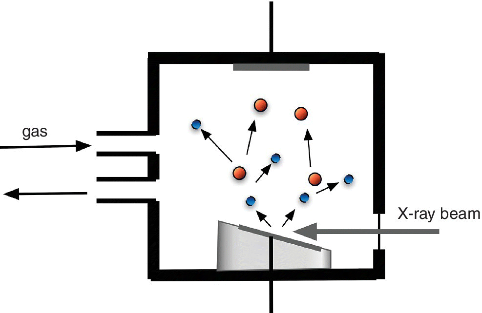
Figure 4.15 Conversion electron/ion yield detection.
4.3.3 Fluorescence
Fluorescence is the most common detection mode for dilute samples. In some sampling designs transmission is not possible, but fluorescence is generally employed when the edge jump is very small (and possibly also on a strongly sloping background). The XAFS features become an extremely small proportion of the total detector signals in the transmission spectrum and thus subject to significant noise. With a low background signal at x‐ray energies below the absorption edge, fluorescence can then provide a better signal/background ratio. However, to achieve this benefit, some energy selection is necessary. This problem is illustrated in Figure 4.16. The most intense peak is from scattering of the incoming x‐ray beam. At the highest energy is the elastically scattered peak, with inelastic effects (Compton scattering) due to momentum transfer from incoming x‐ray to the electrons in the sample. The two smaller peaks are the Kα (7.49 keV) and Kβ (8.25 keV), the intensity of which can be proportional to the x‐ray absorption, under the right sampling conditions.
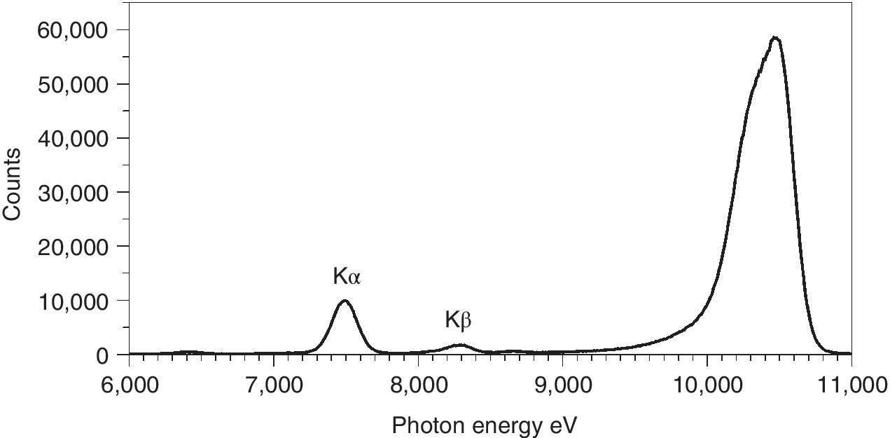
Figure 4.16 Counts measured from a nickel‐containing sample with a multi‐element germanium detector at 90° to the x‐ray path.
(Source: Data from I20, Diamond)
The partitioning between Auger electron and x‐ray emission moves to favor fluorescence with increasing atomic number, and thus absorption edge energy (Figure 4.17: data from [6,7]). The crossover of 50% probability for K emission is from Zn to Ga, but for emission from the L3 edge this point is only reached for transuranic elements. The actual fluorescence yield available for detection is a function of the edge jump, fluorescence yield, and the absorption at both the incoming radiation and the fluorescence channels; the latter will have a shorter attenuation length than the incoming radiation, thus reducing the sampled volume. Each type of sample should be assessed on its own parameters, but the following examples can show some trends.
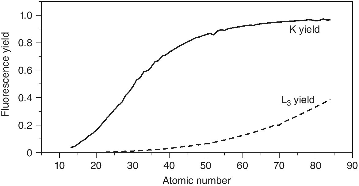
Figure 4.17 The fluorescence yield following absorption at the K and L3 edges as a function of atomic number.
Samples containing germanium (K edge 11.11 keV) and iridium (L3 edge 11.21 keV) will have similar attenuation lengths for the most likely edge of study. Both are convenient edges of study by XAFS, with the energy gap between the L3 and L2 edges of iridium being over 1600 eV. At their attenuation lengths lengths (2.63 mm for Ge and 2.33 mm for Ir), the edge jump of our reference 50 mM aqueous solutions would be 0.17 and 0.27 for Ge and Ir, respectively, in spite of the 13% larger sampling volume for the Ge sample. This higher edge jump for Ir (Ir/Ge = 1.6) is more than compensated by the lower fluorescence yield (Ir/Ge = 0.55), indicating an overall signal ratio of Ir/Ge = 0.9, roughly the ratio of the sample thickness. The reduction in relative sensitivity, however, is amplified by the fact that the α and β fluorescence channels are of lower energy for iridium L (Lα 9175, 9099 eV; Lβ 10708 eV) than those for germanium K (Kα 9886, 9855 eV; Kβ 10982 eV). Accordingly the attenuation lengths of the emissions for iridium (for the 50 mM aqueous solution: at Lα 1.28 and 1.25 mm; at Lβ 2.03 mm) will be shorter than those for germanium (at Kα 1.86, 1.84 mm; at Kβ 2.56 mm); this will reduce the relative number of photons escaping the sampling environment for iridium rather than for germanium. This trend will pertain for comparisons between 3d and 5d transition series.
The second comparison is between the K and L shells of a 4d transition element, taking as an example zirconium, the most abundant element of this transition series in the solar system. The energies of the K and L3 edges are 17998 and 2223 eV, respectively. Hence the attenuation lengths of our sample 50 mM aqueous solution are very different: 21.4 µm and 10.192 mm before the L3 and K edges, respectively. In this case then, the comparisons are very clear. At the sampling depth of the attenuation length, then the ratio of the edge jumps strongly and favors the higher energy edge (K/L3 = 24), and this is amplified when considering the relative fluorescence yield to give a relative sensitivity of K/L3 ~600:1. For thin samples the higher absorbance change per µm at the L3 edge is compensated by the higher fluorescence yield of the K emissions. Given that the energies of the Lα (2042, 2040 eV) and Lβ (2124 eV) will make sample, window, and air absorption very high, and the energy range to the Zr L2 edge is 84 eV, it will be a rare experiment for which the L3 is favored over the K edge. The only advantages of the L edges will be the lower core hole line width (1.57 eV for L3 compared to 3.84 eV for the K edge), and the differing transitions from the 2p core electron that will both give valuable information in the XANES region.
4.3.3.1 Total Fluorescence Yield
The standard geometry for fluorescence detection (Figure 4.18) is designed to optimize the fluorescence signal over the scatter background, by placing the detector away from the x‐ray path. The sample is angled close to 45° to the incoming beam in the horizontal and the effective sample thickness is increased by a factor of √2. The horizontal geometry is chosen since the synchrotron radiation is linearly polarized in that plane and scattering is minimized perpendicular to the incoming beam in the plane of polarization. The x‐ray fluorescence is spread over the full solid angle (4π sr), and thus the geometry in Figure 4.18 normally provides the optimum If/scatter ratio. The global spread of the fluorescence signal means that the collection efficiency is generally limited by the solid angle subtended by the detector from the sampling point.
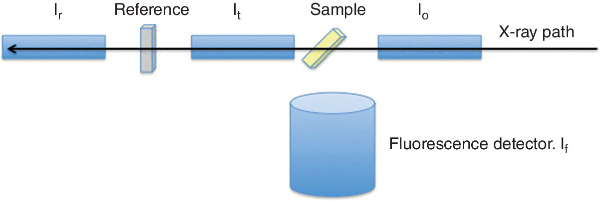
Figure 4.18 Configuration for measuring XAFS in fluorescence in addition to transmission.
The energy difference between the absorption edge and the most intense of the consequential emission lines is about 10% and 20% for K and L3 edges, respectively.
An ion chamber detector, as used in transmission measurements cannot provide the resolution required to distinguish scatter from fluorescence. Inserting a filter between the sample and the detector, can provide this to a significant extent. For many elements, the K edge of the preceding (Z‐1) element in the periodic table lies between the energies of the absorption edge and the Kα emissions (Table 4.1). In that case the mass absorption of the filter will be low at the Kα energy allowing the fluorescence to pass with little attenuation, but it will absorb a high proportion of the exciting radiation, thus increasing the If/background ratio (equation 4.10). Thus the signal/noise ratio can be improved if the background signal Ib is decreased or the acquisition time, t, is increased.
Table 4.1 Energies (keV) of edges and emissions of the K absorption of the elements of the first long period and of potential Z‐1 filters for fluorescence measurements. Gray shading indicates degree of problems monitoring with the emission line using the suggested filter.
| Element | K | Kα1 | Kβ1 | Filter | K | Kα1 | Kβ1 |
| Calcium | 4.04 | 3.69 | 4.01 | Potassium | 3.61 | 3.31 | 3.59 |
| Scandium | 4.49 | 4.09 | 4.46 | Calcium | 4.04 | 3.69 | 4.01 |
| Titanium | 4.97 | 4.51 | 4.93 | Scandium | 4.49 | 4.09 | 4.46 |
| Vanadium | 5.47 | 4.95 | 5.43 | Titanium | 4.97 | 4.51 | 4.93 |
| Chromium | 5.99 | 5.41 | 5.95 | Vanadium | 5.47 | 4.95 | 5.43 |
| Manganese | 6.53 | 5.90 | 6.49 | Chromium | 5.99 | 5.41 | 5.95 |
| Iron | 7.11 | 6.40 | 7.06 | Manganese | 6.53 | 5.90 | 6.49 |
| Cobalt | 7.71 | 6.93 | 7.65 | Iron | 7.11 | 6.40 | 7.06 |
| Nickel | 8.33 | 7.48 | 8.26 | Cobalt | 7.71 | 6.93 | 7.65 |
| Copper | 8.98 | 8.05 | 8.91 | Nickel | 8.33 | 7.48 | 8.26 |
| Zinc | 9.66 | 8.64 | 9.57 | Copper | 8.98 | 8.05 | 8.91 |
| Gallium | 10.37 | 9.25 | 10.26 | Zinc | 9.66 | 8.64 | 9.57 |
| Germanium | 11.10 | 9.89 | 10.98 | Gallium | 10.37 | 9.25 | 10.26 |
| Arsenic | 11.87 | 10.54 | 11.73 | Germanium | 11.10 | 9.89 | 10.98 |
| Selenium | 12.66 | 11.22 | 12.50 | Arsenic | 11.87 | 10.54 | 11.73 |
| Bromine | 13.47 | 11.92 | 13.29 | Selenium | 12.66 | 11.22 | 12.50 |
| Krypton | 14.33 | 12.65 | 14.11 | Bromine | 13.47 | 11.92 | 13.29 |
A favorable example would be the use of a copper foil as a filter for the Zn Kα fluorescence (Figure 4.19). The sample is modeled as a thin Zn sample with a transmission change at the edge from 0.97 to 0.83. The thicker copper foil (10 µm) has a transmission change from 0.72 to 0.078 at its edge. At the zinc Kα energy, the Cu foil would provide a transmission of 0.69, thus removing about 30% from passing to the detector. For the Kβ line, the filter will attenuate the signal by 0.89. The scatter over the whole of a likely pre‐edge range and a full EXAFS run will be attenuated significantly (90–82%). The If/scatter ratio will have improved by this filter as the scatter has been attenuated much more, but the problem has not been eliminated. The scatter can be attenuated more with a thicker foil (by 95% for a 25 µm thickness), but at the expense of reducing the transmission of the Kα emission (to 40%).
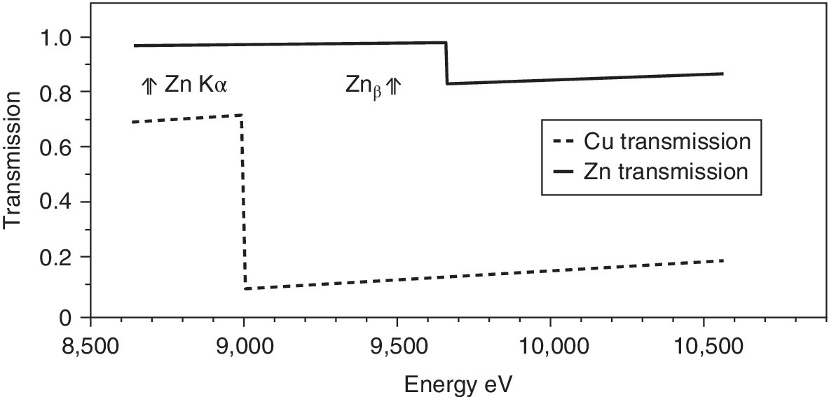
Figure 4.19 X‐ray transmission of a 1 µm zinc “sample” with the effect of a 10 µm copper foil as a filter.
For other elements, there is more difficulty in finding an effective filter (Table 4.1); for elements early in the first long period, there is no capacity for creating an unperturbed pre‐edge or edge structure. The Z‐1 formula does not hold across for the L3 edges of the third long period (Table 4.2). However, gaps can be filled by exploiting the K edges of lighter elements and, for a few metals, the Lβ as well as the Lα channel can be enhanced significantly over the background scatter.
Table 4.2 Energies (keV) of edges and emissions of the L3 absorption of elements of the third long period and potential filters for fluorescence measurements. Gray shading indicates degree of problems monitoring with the emission line using the suggested filter.
| Element | L3 | Lα1 | Lβ1 | Filter | K/L3 | Kα1/Lα1 | Kβ1/Lβ1 |
| Barium | 5.25 | 4.66 | 4.83 | Titanium | 4.97 | 4.51 | 4.93 |
| Lanthanum | 5.48 | 4.65 | 5.04 | Titanium | 4.97 | 4.51 | 4.93 |
| Hafnium | 9.56 | 7.90 | 9.02 | Copper | 8.98 | 8.05 | 8.91 |
| Tantalum | 9.88 | 8.15 | 9.34 | Copper | 8.98 | 8.05 | 8.91 |
| Tungsten | 10.21 | 8.40 | 9.67 | Tantalum | 9.88 | 8.15 | 9.34 |
| Rhenium | 10.54 | 8.65 | 10.01 | Tungsten | 10.21 | 8.40 | 9.67 |
| Osmium | 10.87 | 8.91 | 10.36 | Tungsten | 10.21 | 8.40 | 9.67 |
| Iridium | 11.22 | 9.18 | 10.71 | Germanium | 11.10 | 9.89 | 10.98 |
| Platinum | 11.56 | 9.44 | 11.07 | Germanium | 11.10 | 9.89 | 10.98 |
| Gold | 11.92 | 9.71 | 11.44 | Germanium | 11.10 | 9.89 | 10.98 |
| Mercury | 12.28 | 9.99 | 11.82 | Gold | 11.92 | 9.71 | 11.44 |
| Thallium | 12.66 | 10.27 | 12.21 | Gold | 11.92 | 9.71 | 11.44 |
| Lead | 13.04 | 10.55 | 12.61 | Gold | 11.92 | 9.71 | 11.44 |
| Bismuth | 13.42 | 10.84 | 13.02 | Lead | 13.04 | 10.55 | 12.61 |
| Polonium | 13.81 | 11.13 | 13.48 | Bismuth | 13.42 | 10.84 | 13.02 |
| Astatine | 14.21 | 11.43 | 13.88 | Bismuth | 13.42 | 10.84 | 13.02 |
| Radon | 14.62 | 11.73 | 14.32 | Bismuth | 13.42 | 10.84 | 13.02 |
These selectivity gains, however, are partially ameliorated by emissions from the filter (Tables 4.1 and 4.2). To reduce that effect, a set of collimating slits (Soller slits) can be mounted between the sample and the detector[8] (Figure 4.20). The fluorescence from the filter foil will be spread over the entire solid angle and so the majority of this unwanted background can be trapped by the collimating slits while allowing the majority of the fluorescence on the path from the sample to the detector to continue. In the example in reference,[2] Fe in a photosynthetic bacterial sample, the effective gain of the filter and the filter‐slit assembly were estimated to be 2.6 and 6.4, respectively. In practice the gain was higher since the reduction in the background allowed the sample‐detector distance to be reduced without saturation of the detector, and thus a larger solid angle of fluorescence could be collected.
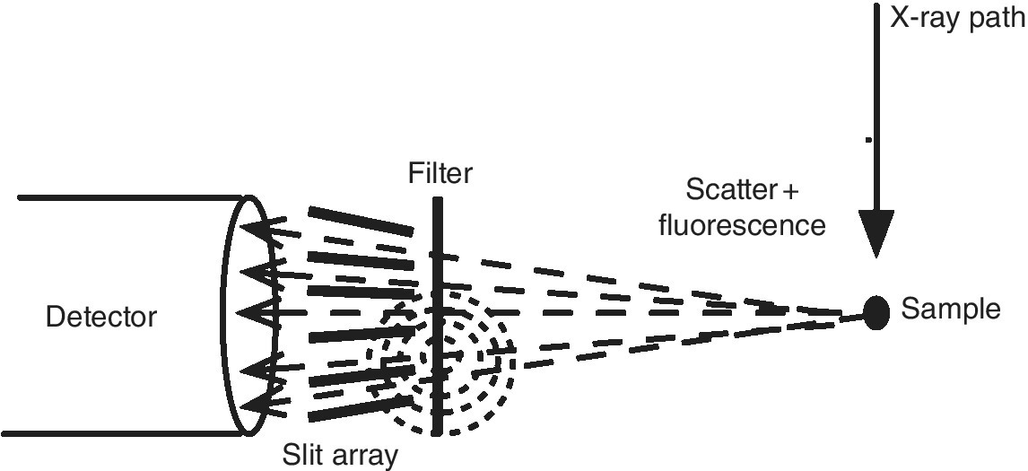
Figure 4.20 Schematic of a filter and Soller slit assembly in front of a fluorescence detector.
As for transmission measurements (Section 4.3.1), there are solid‐state alternatives to ion chambers. Photodiodes may be employed, and avalanche photodiodes (APDs) for fast detection (ns). Neither of these is energy selective, and thus may also require a filter‐slit assembly to improve the signal/noise ratio. Neither has the advantage of the controllable intrinsic sensitivity control of an ion chamber, through (partial) gas pressures. Also, each can suffer from crystal glitches within the detector.
Energy discriminating solid‐state systems are generally the detectors of choice. The detector diode element may be based on silicon (e.g., in a drift diode), or on germanium (e.g., a pin diode). The latter is a more absorbing material, an advantage at higher x‐ray energies. These are more complex pieces of instrumentation, with arrays of diodes gathered in a detector head to increase the solid angle that is collected (Figure 4.21). Both require the detector head to be cooled during use. For silicon‐based systems cooling can be afforded by a thermoelectric device, but liquid nitrogen temperatures are essential for the germanium.
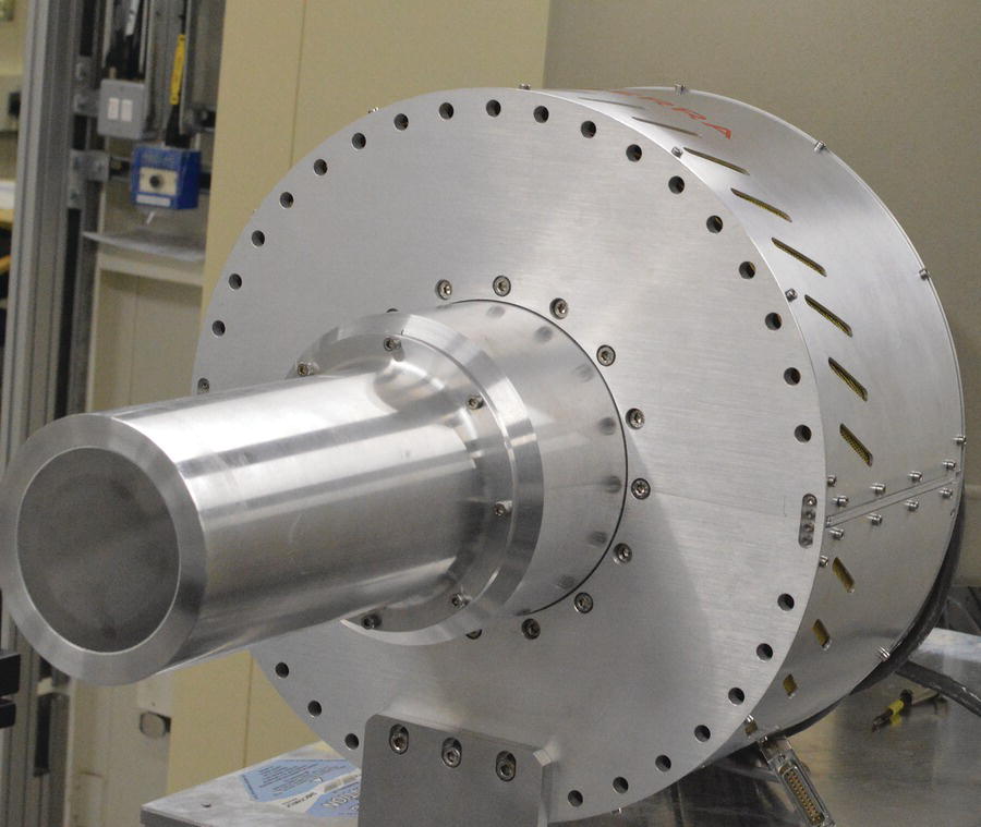
Figure 4.21 64‐element germanium detector on I20.
(Source: Diamond)
Returning to the example of the nickel spectrum in Figure 4.16, we can see that the Kα energy for Ni is ~500 eV to lower energy of a typical XAFS scan (Ni K edge 8333 eV) (Figure 4.22). Energy discriminating detectors can afford resolutions in the range of ~130–300 eV, and thus can be used to isolate the signal due to the Kα1 and Kα2 lines from the background elastic scatter, and the Kβ emission.
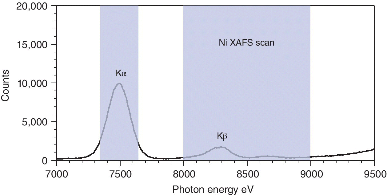
Figure 4.22 Fluorescence and scatter signals from a Ni‐containing sample with a multi‐channel analyzer (MCA) highlighting the energy window of a XAFS scan and also of selective Kα monitoring.
(Source: Data from I20, Diamond)
The principle behind the detector is illustrated in Figure 4.23. The absorption of an x‐ray photon resulting in a cascade of electron hole pairs in the diode. The number of pairs is related to the x‐ray energy (Section 4.3.1) and thus forms a measure of that energy. Thus the magnitude of the Gaussian curves in the figure relate to the measurement of these events using a multichannel analyzer (MCA). The resolution of the time difference relates to the count rate that can be accommodated by the detector before saturation. This is limited by the peaking time of the device. Silicon drift devices can be obtained with a peaking time of 0.1 µs, giving a count rate of 900 kHz. This high count‐rate is obtained at the expense of energy resolution; the precision of the electron‐pair count deteriorates with a shorter acquisition time. For an authentic XAFS spectrum, it is wise to keep below the saturation limit to ensure a linear response, and a count rate of 100 kHz per diode is generally safe.
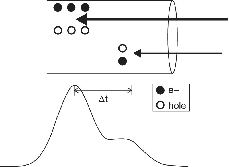
Figure 4.23 Events related to two x‐ray photons of different energy impacting on a diode in an energy discriminating detector.
Under ideal conditions, ratio of the fluorescence signal, If, to the incoming radiation, I0, is proportional to the x‐ray absorption (equation 4.11). And so it can be expected that this is a straightforward means of measuring a XAFS spectrum. However, this only holds for particular conditions: dilute and/or thin. In these conditions, for example, a complex of a heavy element, for example, silver dissolved in a light‐atom matrix, for example, water, the absorption due to the matrix is essentially constant across the spectrum (Ag K edge 25.5 keV) and the thickness sampled is unchanged. The sample would be oriented to maximize If, with the sample set at 45° to the incoming beam (θ = ϕ = 45° in Figure 4.24).
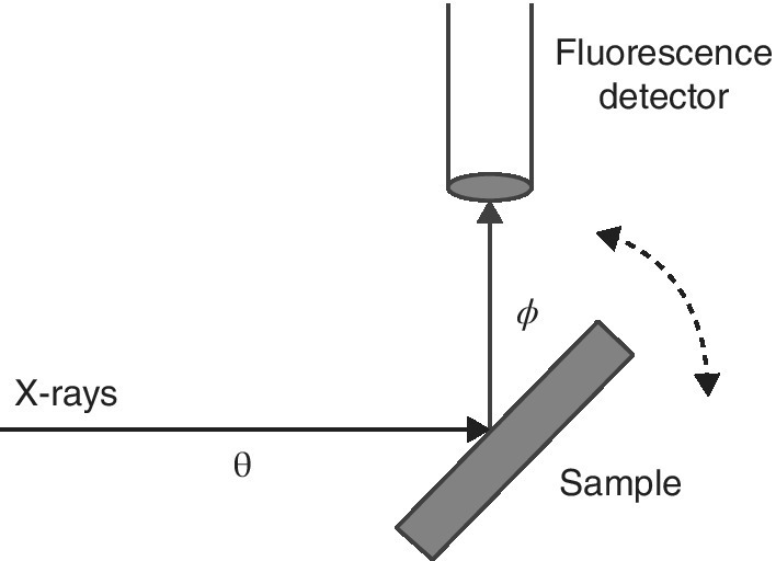
Figure 4.24 Sample orientation variation in a fluorescence measurement.
However, if the sample is significantly absorbing, then the penetration depth will increase with energy above the edge. The fluorescence photons, for example, Kα are of an energy close to the low point of the mass absorption of an element just before the edge. If the sample is concentrated then the fluorescence yield will increase significantly with photon energy. This will make the background subtraction more difficult but it also has the effect of dampening the EXAFS features so reducing the apparent coordination number. One way to reduce these sample absorption effects is to rotate the sample close to normal to the incoming beam such that ϕ ~ 0 (grazing exit). That will strongly reduce the signal reaching the detector, but it will remove the energy dependence giving the relationship in equation 4.12, where μtotal(Ef) is the mass absorption of the entire sample at the energy of the fluorescence.
Alternatively, if the sample is thin, and observed at grazing incidence (θ ~ 0), then the If/I0 is proportional to sample x‐ray absorption and the thickness (equation 4.13). Grazing incident angle XAFS is an established technique for investigating thin films, often in tandem with x‐ray reflectivity measurements. The maximum sensitivity is obtained if θ is just under the critical angle.[9]
4.3.3.2 High‐Resolution Fluorescence Detection (HERFD) and X‐Ray Emission Spectroscopy (XES)
In the previous section, we started with the detection of the total x‐ray fluorescence yield, and with energy discriminating detectors arrived at the capability of windowing onto a set of closely spaced transitions, for example, Kα1 plus Kα2. Improving the energy resolution further will allow the refinement of investigating these two channels independently. To achieve that resolution the emission spectrum is discriminated using a crystal analyzer in a secondary spectrometer (Figure 4.25). The analyzer crystal is bent to the radius of curvature of the Rowland circle that also includes the sample and detector.[10] The circle may be close to the horizontal or vertical planes and may also be stacked with a series of analyzer crystals to increase the solid angle of collection and thus the sensitivity.[11,12] In some installations a small position sensitive detector is used as it eases greatly the alignment of the optical system.
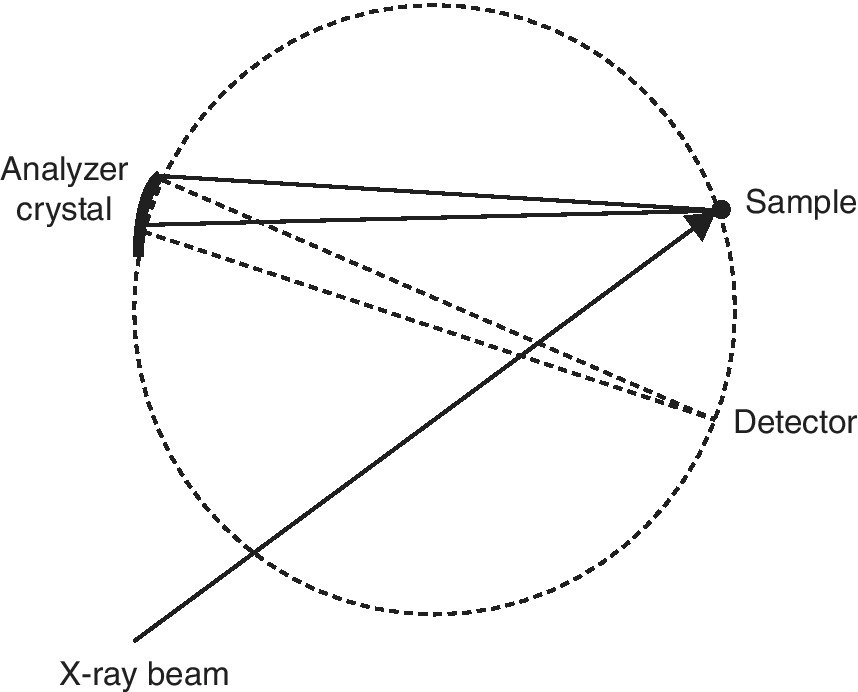
Figure 4.25 Johann geometry for energy resolution of the emission from a sample using a point detector.
The resolution is achieved using a very high Bragg angle, and benefits from a small source size. Energy scanning in the secondary spectrometer is achieved by rotating the monochromators onto a new position on a Rowland circle and translating the detector to keep it on the new circle. A suite of crystals is required to cover different emission lines (Table 4.3). The path length of the fluorescence signal is considerably increased, depending upon the radius of the Rowland circle. To avoid strong signal loss to the absorption by air, these spectrometers are generally mounted within a helium‐filled shroud. Such an arrangement is shown in Figure 4.26.
Table 4.3 Examples of crystal reflections and diffraction angles required the measure the x‐ray emission spectra of some emissions of 3d elements (as for I20, Diamond).
| Element | Kα1 (eV) | Reflection, θ° | Kβ1 (eV) | Reflection, θ° |
| Ti | 4511 | 4932 | Si(400), 67.805 | |
| V | 4952 | Si(400), 67.217 | 5427 | Ge(422) 81.525 |
| Cr | 5415 | Ge(422), 82.424 | 5947 | Si(333), 85.812 |
| Mn | 5899 | Si(422), 71.403 | 6490 | Si(440), 84.199 |
| Fe | 6404 | Ge(440), 75.398 | 7058 | Si(531), 73.038 |
| Co | 6930 | Si(531), 77.018 | 7649 | Ge(444), 82.887 |
| Ni | 7478 | Si(620), 74.881 | 8265 | Si(444), 73.104 |
| Cu | 8048 | Si(444), 79.342 | 8905 | Si(642), 73.58 |
| Zn | 8639 | Si(642), 81.397 | 9572 | Ge(660), 76.288 |
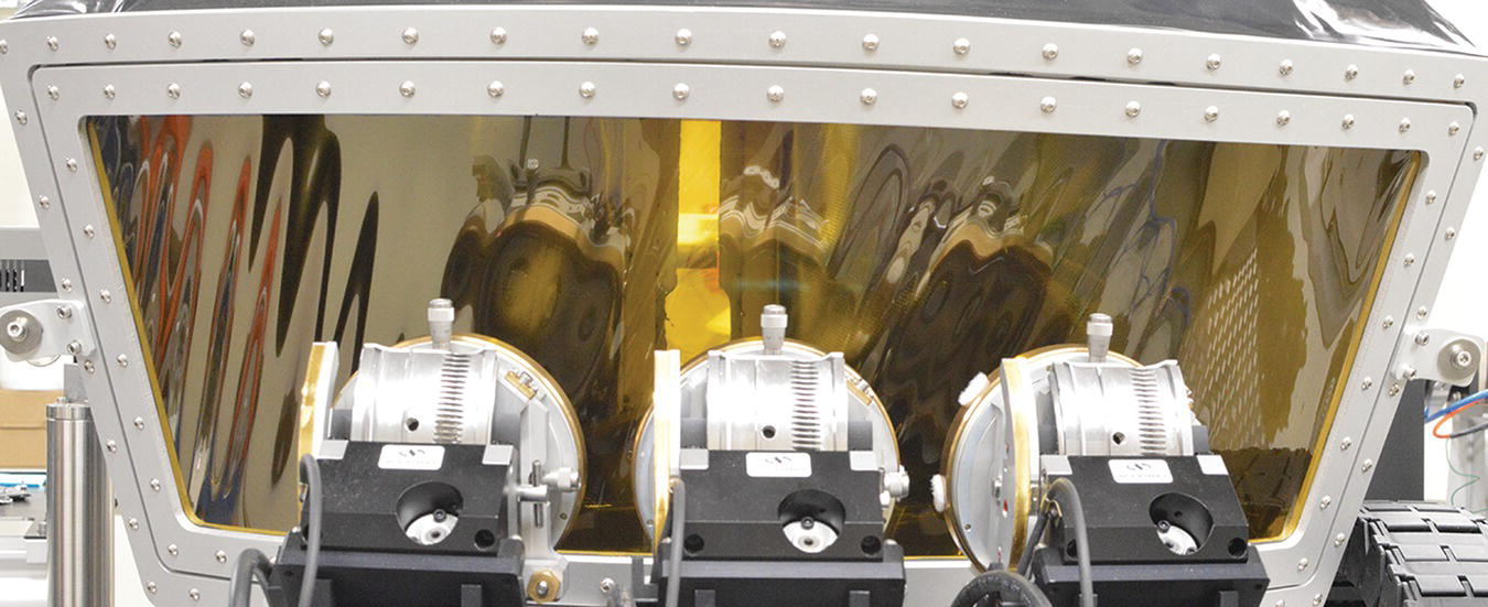
Figure 4.26 View over mount for three‐analyzer crystals through the helium shroud to the sample position.
(Source: Diamond, I20)
The x‐ray emission spectra of copper metal and its oxides (Figure 4.27) show little structure, with only a small shift (< 1 eV) to higher energy. Such scans can provide the optimum emission energy to maximize the sensitivity of fluorescence detection for each sample. An important observation was that the XANES features that were observable using this partial fluorescence yield method of detection, which has a much higher resolution that the width of the emission line, were considerably sharper than those recoded by transmission or by total fluorescence yield,[13] and the technique is now termed high‐energy resolution fluorescence detection (HERFD). In the XANES region, the lifetime broadening is dominated by the core‐hole after the emission. In the case of Kα1 emission, the most intense, that will be the L3 level. The core‐hole line‐widths for Cu 1.55 and 0.56 eV for the K and L3 shells, respectively. The effects are illustrated in Figure 4.28 for the two copper oxides. The sharpness of the edge features makes discrimination between the two oxidation states very clear. Also, by reducing the background slope of the intense features to low energy, weak pre‐edge features (for CuO) can be identified more obviously. Above the XANES region line‐width sharpening is lost and there is rarely a gain in recording EXAFS in this way rather than by an energy‐selective detector that will generally have a larger solid angle and fluorescence signal.
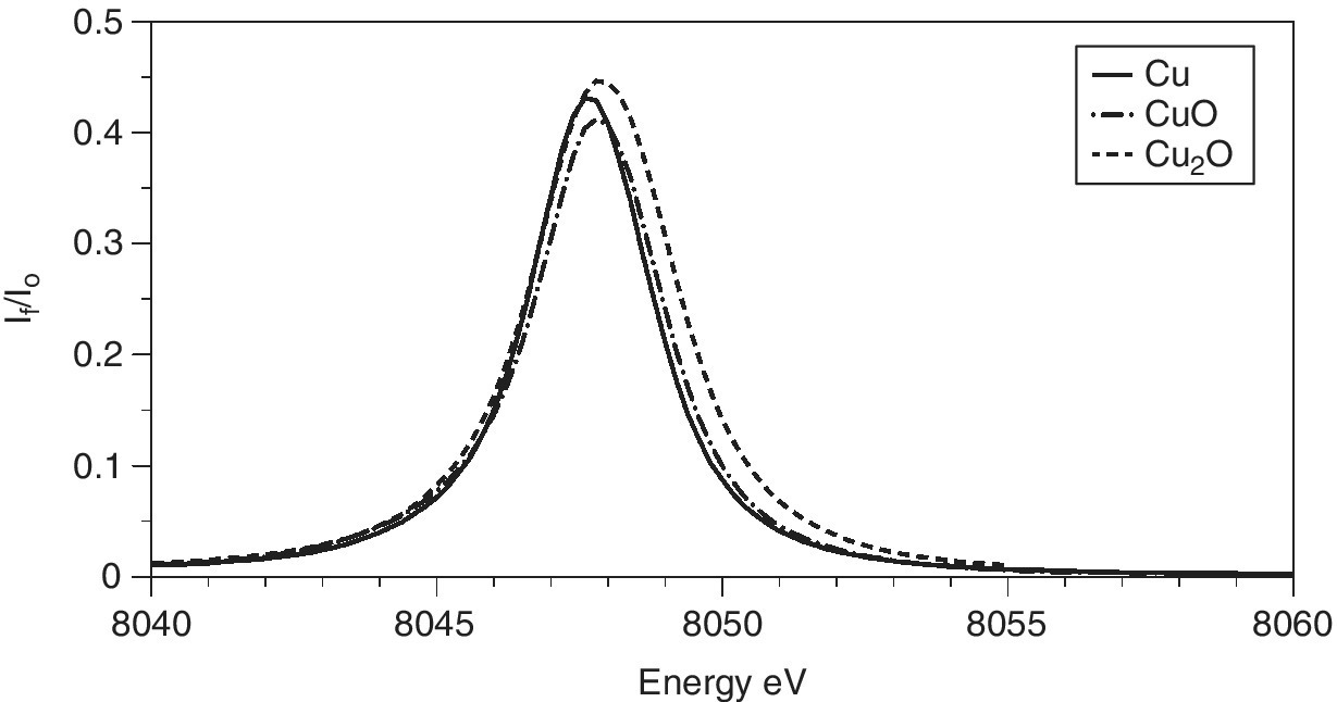
Figure 4.27 Kα1 x‐ray emission spectra of Cu, Cu2O, and CuO recorded with a four‐bounce Si(111) monochromator for I0 and three Si(444) XES analyzer crystals.
(Source: Diamond, I20)
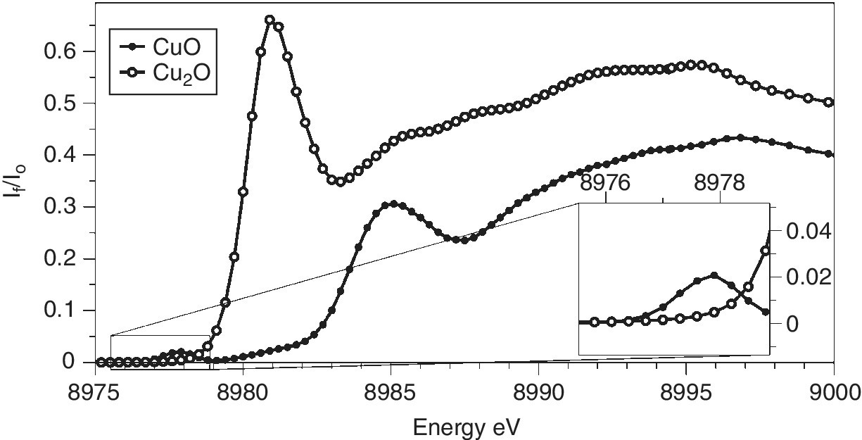
Figure 4.28 K edge HERFD of copper oxides detected using the Kα1 emission line of copper.
(Source: Diamond, I20)
Other emission lines can also be monitored. In the K series, as is illustrated in Figure 4.29 for copper, the relative intensity follows an order:

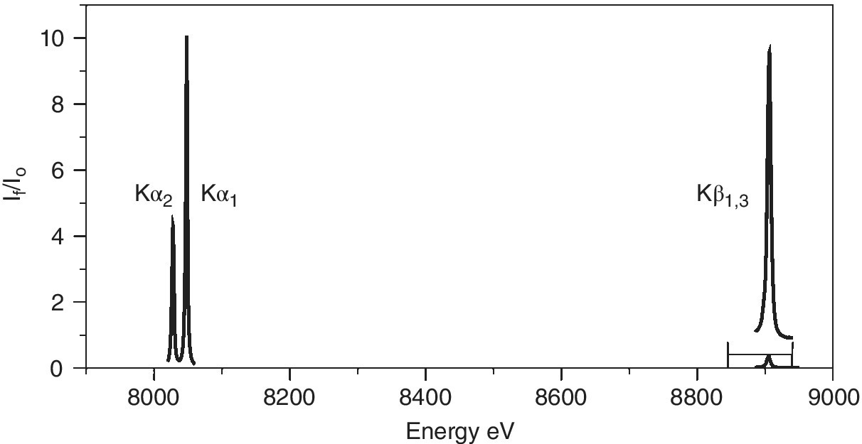
Figure 4.29 K emission lines of copper metal.
(Source: Diamond, I20, data from Roberto Boada‐Romero)
It is evident that the line‐width of the Kβ1,3 emission is rather wider than that of the two Kα lines. A comparison of the HERFD of copper foil measured with the Kα1 and Kβ1,3 emissions is shown in Figure 4.30. The resolution also appears to be better for the former, more intense feature. For these spectra, the widths of the elastic peak were ~1.2 and ~1.7 eV, respectively, for Kα1 and Kβ1,3. One factor for this is the different resolutions achievable for these lines with the emission spectrometer. The Kα1 line was measured using Si(444) reflections at 79.3174°, which ideally gives a resolution of 0.026 eV/mdeg; the lower Bragg angle employed for the Kβ1,3 emission (73.5809°) results in a lower resolution (0.047 eV/mdeg) in spite of the higher order reflection (642). However, the core‐hole lifetimes will also contribute.[14,15] The natural widths (Γ) of the fluorescence lines are closely related to those of the two states involved.


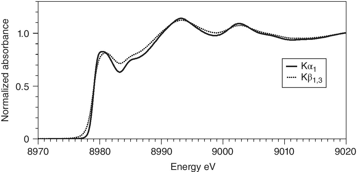
Figure 4.30 Cu K edge HERFD of copper foil measured with emissions from Kα1 (8047.8 eV, 4 scans) and Kβ1,3 (8905.3 eV, 12 scans).
(Source: Diamond, I20)
When the exciting energy is close to threshold (Eo), the emission broadening is reduced[13,16] and can approach a FWHM of 2 Γ(L3) for the Kα1 emission (and 2 Γ(M2,3) for Kβ1,3). The natural line‐widths of the K and L3 edges of copper are 1.55 and 0.56 eV, respectively. A sharpening of the XES line to ~1.2 eV near the absorption edge is attainable, and thus affords the improved resolution of the HERFD spectrum (Figure 4.28). However, the widths due to lifetimes of the core‐holes of the M2/3 edges (1.6 eV) are very similar to that of the K edge, and in this case Kβ1,3 HEFRD does not improve the resolution of the XANES region over a conventional transmission spectrum.
4.3.3.3 Resonant Inelastic X‐Ray Scattering or Spectroscopy (RIXS)
The capability of scanning both incoming and outgoing radiation opens up new possibilities. As can be seen for CuO (Figure 4.31), the shape of the emission spectrum varies with excitation energy. Using the excitation energy that affords the maximum emission (8995 eV), a single line is observed. Lowering the excitation energy not only reduces the total emission, but it also changes the shape of the emission curve. Mapping the variations in emission with both excitation and emission energy are experimentally feasible by stepping though those energies on the primary and secondary crystal spectrometers, respectively. The technique is variously described as RIXS (Resonant Inelastic X‐Ray Scattering or Spectroscopy) or RXES (Resonant X‐Ray Emission Spectroscopy).[17,18]
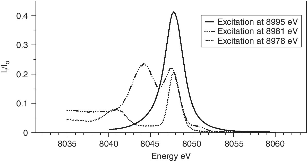
Figure 4.31 Kα1 emission spectra of CuO with three excitation energies. The XES with the two lower energy excitations are amplified by a factor of 10.
(Source: Diamond, I20)
The measurement of RIXS data is achieved by recording a series of XAFS spectra with a stack of emission energies, and the natural way to present this is as in Figure 4.32a. Here there is a contour map of the If /I0 values for the energy of incoming and outgoing x‐radiation. The horizontal line through the emission maxima (Figure 4.31) is the HERFD spectrum in Figure 4.28. The vertical lines will be emission spectra measured at different excitation energies. The variations shown in Figure 4.31 can be envisaged as coming from different slices through the structured patterns below an excitation energy of ~8990 eV.

Figure 4.32 Kα1 RIXS spectra of CuO plotted with 32 contours of If/I0. Axes used are the excitation and a) emission or b) transfer energies.
(Source: Diamond, I20)
There is an alternative presentation intrinsic to the inelastic scattering associated with the overall process. In that the y‐axis takes the form of the difference between the excitation and emission energies, which is the energy transferred to the sample as it is converted into an excited sate with a 2p core hole (Figure 4.32b). In this representation the HERFD spectrum is the diagonal through the maxima. In both representations of RIXS, the pre‐edge peak evident in the HERFD spectrum can be seen to be a resonance to low energy of the absorption edge along the line of constant emission energy (CEE). Here vertical lines represent emission spectra at constant incident energy (CIE) and the horizontal lines XAFS spectra at constant emission energy (CEE).[17,18]
The RIXS patterns are very sensitive to oxidation state and coordination number. Comparison between the plots in Figure 4.33 show very distinct differences for the linear CuI site in Cu2O and the tetrahedral [Cu(dmp)2]+ near 8992 eV. For the oxide the pre‐edge feature is very intense and to relatively low energy. In the linear geometry two of the 4p orbitals are non‐bonding and thus provide the route to a relatively low energy dipole allowed transition. In the tetrahedral example these orbitals will largely have copper‐nitrogen antibonding character, and so be raised in energy. This complex also showed a small pre‐edge resonance, about 2 eV higher in energy than that observed for CuO (Figure 4.31).
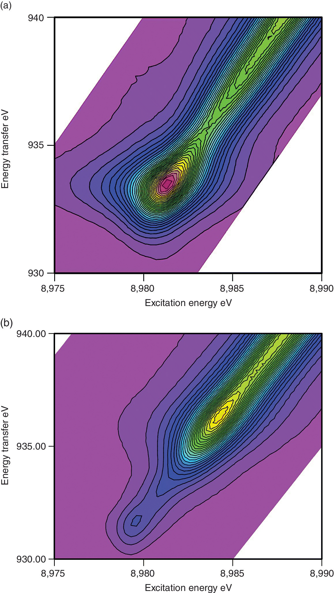
Figure 4.33 Kα1 RIXS spectra with 32 contours of If/I0 of two Cu(I) samples. a) Cu2O b) [Cu(dpm)2]PF6 (dpm = 2,9‐dimethyl‐1,10‐phenanthroline).
(Source: Diamond, I20)
4.3.3.4 Inelastic X‐Ray Raman Scattering (XRS) or Nonresonant Inelastic X‐Ray Scattering (NIXS)
The range of inelastic scattering process that can be monitored with secondary spectrometers is large. It is very dependent upon the resolution of the monochromator, so electronic and vibrational processes can be identified with sufficiently high resolution (sub eV to meV). With a resolution typical of the XES and RIXS measurements described above, then features with an energy transfer of a few 10s and 100s of eV have been identified as the absorption edges of low Z‐elements in the sample.[19,20] A demonstration example is provided by the observation of the carbon K edges of graphite and diamond (Figure 4.34). This was using excitation energies of 8400 or 8900 eV. Clearly sensitivity is challenging, but installations are in place with multiple analyzer‐detector arrays to enhance the solid angle that can be collected for a particular energy loss at different scattering angles [21]. As a result, it has become feasible to investigate the structures of light elements within bulk materials, such as the study of lithium and oxygen in discharged electrodes.[22]
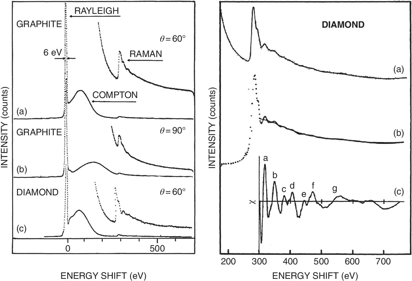
Figure 4.34 Inelastic scattering spectra Left: a) of graphite at 60° excited at 8900 eV, b) of graphite at 60° excited at 8900 eV, c) of diamond at 60° excited at 8400 eV. Right: Extraction of the C K edge EXAFS of diamond.
(Source: Tohji 1989.[20] Reproduced with permission of American Physical Society)
4.3.4 X‐Ray Excited Optical Luminescence (XEOL)
In addition to stimulating x‐ray fluorescence, x‐ray absorption can, for some samples, give rise to a detectable emission in the uv‐visible region. The arrangement for the detection of such emissions is very similar to that for x‐ray fluorescence.[23] The fluorescence can be collected via a lens and then passed into a box shielding the detector from x‐radiation (Figure 4.35). The XEOL effect can be used as a measure of x‐ray absorption, selecting the energy of interest with an optical filter, and then passing through to a photomultiplier tube or photodiode; this is analogous to having an energy selective x‐ray detector. Alternatively, using an optical monochromator, element‐selective optical emission spectra can be recorded. In addition, the emission may be due only a portion of the sites adopted by the element being studied, and so the method will afford site selective XAFS. An example is the selection between recording the XANES of ZnO or ZnS by selecting appropriate emission wavelength (510 and 575 nm, respectively).[24]
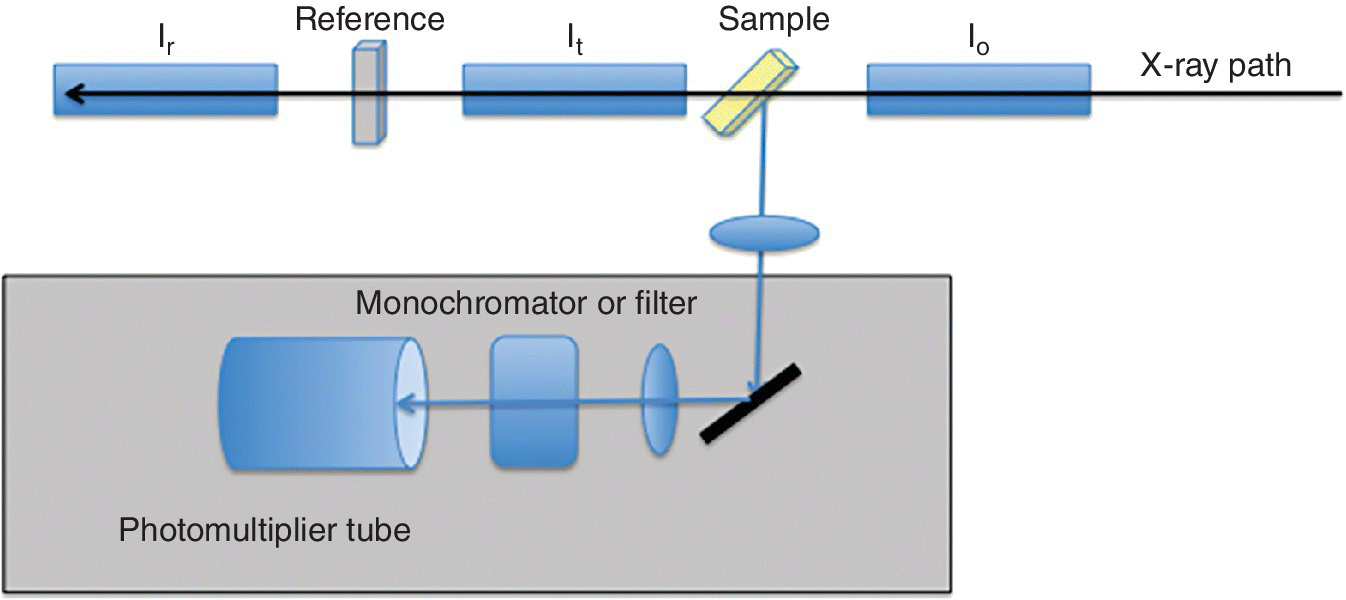
Figure 4.35 Schematic of instrumentation for carrying out x‐ray excited optical luminescence (XEOL).
Such instrumentation[25] was employed to probe the nature of nanocrystalline germanium prepared by laser ablation and other methods.[26] The wavelength of the optical emission was very dependent upon the mode of sample preparation. Laser ablation providing an XEOL signal around ~700 nm that could be using to record optically detected (OD) XAFS spectra (Figure 4.36). Although the conventionally measured XAFS spectrum indicated elemental germanium predominated in the sample, the source of the emission could be ascribed to GeO2. Time‐resolved XEOL effects can also be measured,[25] as illustrated by the recording of Eu L3 edge XANES of Eu2O3 from both short‐lived (360 nm) and long‐lived (610 nm) states.
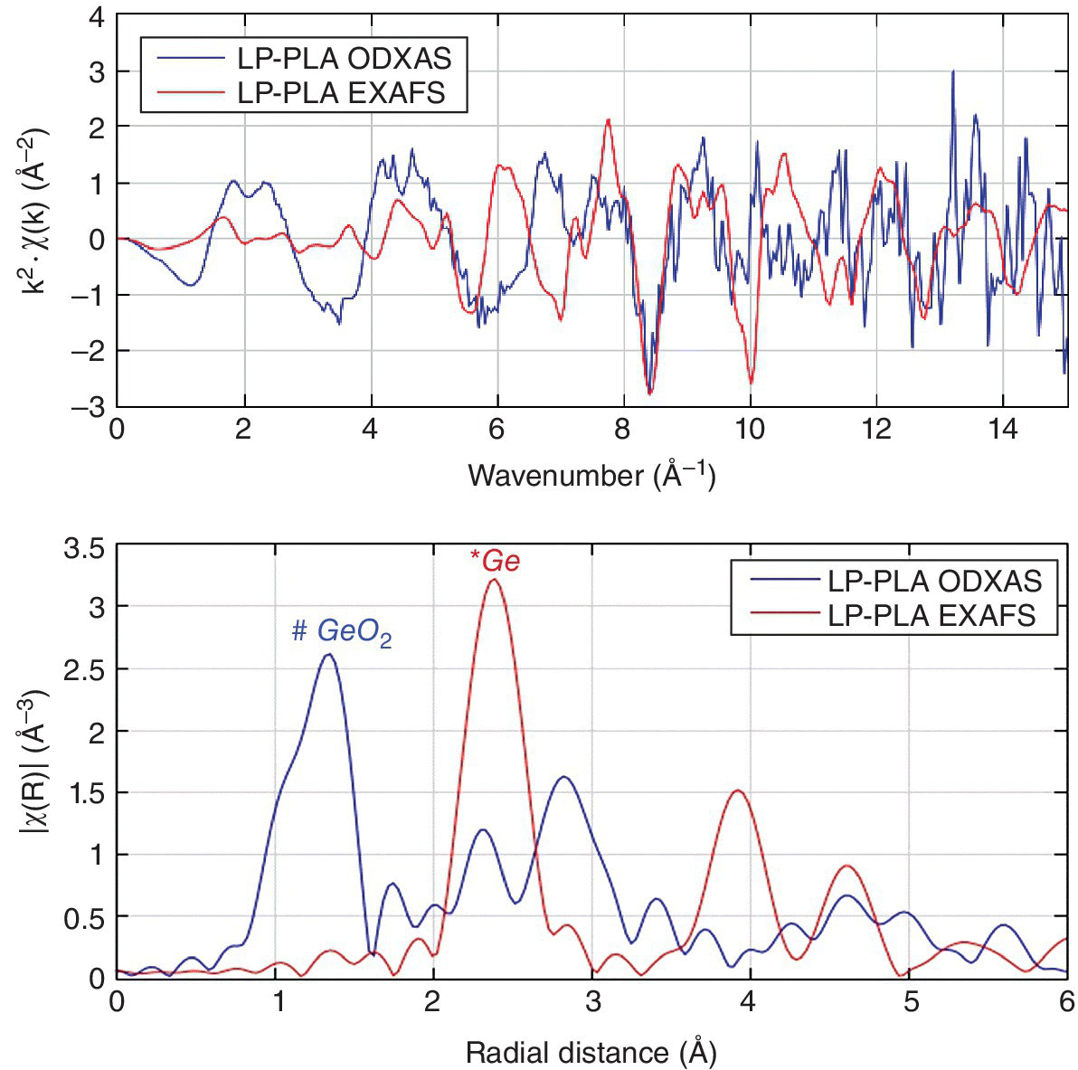
Figure 4.36 Comparison of the optically detected (OD) (700 nm emission) and transmission Ge K edge EXAFS (top) and Fourier transform (bottom) of nanocrystalline germanium prepared by laser ablation (LP‐PLA).
(Source: Courtesy of Andrei Sapelkin, Queen Mary University)
4.4 Spatial Resolution
4.4.1 Methods of Studying Textured Materials
The most common methods of investigating the composition of materials with a resolution of microns or nm are scanning and transmission electron microscopy. At one level this provides a measure of the electron density of voxels in a material, but with the addition of an x‐ray fluorescence analyzer, the maps can show elemental composition. In principle, the techniques described so far can be adapted to mapping of sites within a textured material, although in practice there are limitations, most commonly of sensitivity. Chemical or site speciation could be envisaged by variation in XANES, XMCD, or XEOL properties. The two main methods are full field, in which the spatial resolution is derived after the sample, and scanning‐transmission where a highly focused beam is tracked across the sample.
4.4.2 Full‐Field Transmission X‐Ray Microscopy (TXM)
A schematic of a full field transmission x‐ray microscope (TXM) is shown in Figure 4.37. The source used is a bending magnet. Generally this has been preferred over an undulator for this approach. The smaller beam size of an undulator increases the space over which the x‐ray beam has high degree of coherent character. This can result in interference fringes from any element in the x‐ray path and thus can introduce artifacts into the image of the sample itself. For this beamline a capillary system is used to focus the beam size allowing illumination of the sample over a 20‐µm range. The transmitted beam is refocused by a zone‐plate onto an imaging detector providing a spatial resolution of ~35 nm. The image is acquired using a monochromatic beam at a single energy, here with a resolving power of 1000. An important use for such a microscope is for biological samples in an aqueous medium. In that case, the using the “water window” provides considerable advantage. The attenuation length of water rises from 0.8 µm near 200 eV to 10 µm just below the K absorption edge of oxygen. The x‐ray transmission of an organic sample is modeled in Figure 4.38 by 1 µm of ethanol. Near 500 eV the reduction in transmission caused by this is ~50%, and thus there is considerable scope for absorption contrast with a relatively transparent background. Samples can be cryo‐cooled, which enhances the stability under x‐radiation. The samples may also be tilted to generate a series of images. A three‐dimensional tomograph of the sample can be generated from the tilt‐series.[27]

Figure 4.37 Schematic of a soft x‐ray full‐field transmission x‐ray microscope.
(Source: Diamond, B24)
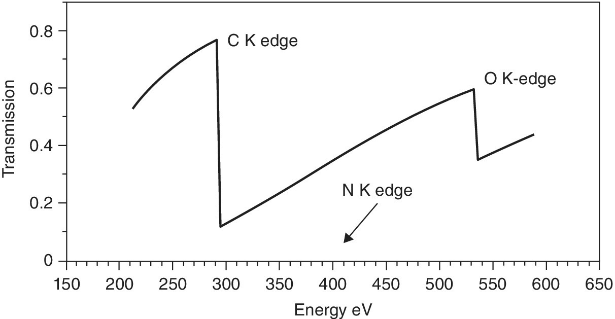
Figure 4.38 Transmission calculated for a 1 µm sample of ethanol in the C, N, and O K edge regions.
An example of application is the imaging of a neuron‐like mammalian cell line (PC‐12) expressing huntingtin exon fragments (Figure 4.39) The huntingtin gene is associated with Huntington’s disease; this sample was prepared by Wei Dai, in the lab of Wah Chiu, at Baylor College of Medicine, Houston, Texas, and imaged by Michele C. Darrow, in the laboratory of Elizabeth M.H. Duke, at Diamond. The beamline in question operates with x‐ray energy of 500 eV with a stable sampling arrangement to allow for rapid image acquisition. The figure shows a slice of a reconstructed three‐dimensional volume from absorption contrast images collected by cryogenic tomography. The image clearly shows the major components of the cell. Some of the organelles (mitochondria, lipid droplets, and autophagosomes) can be identified by their characteristic features. The large organelle near to the nuclear membrane was of particular interest.
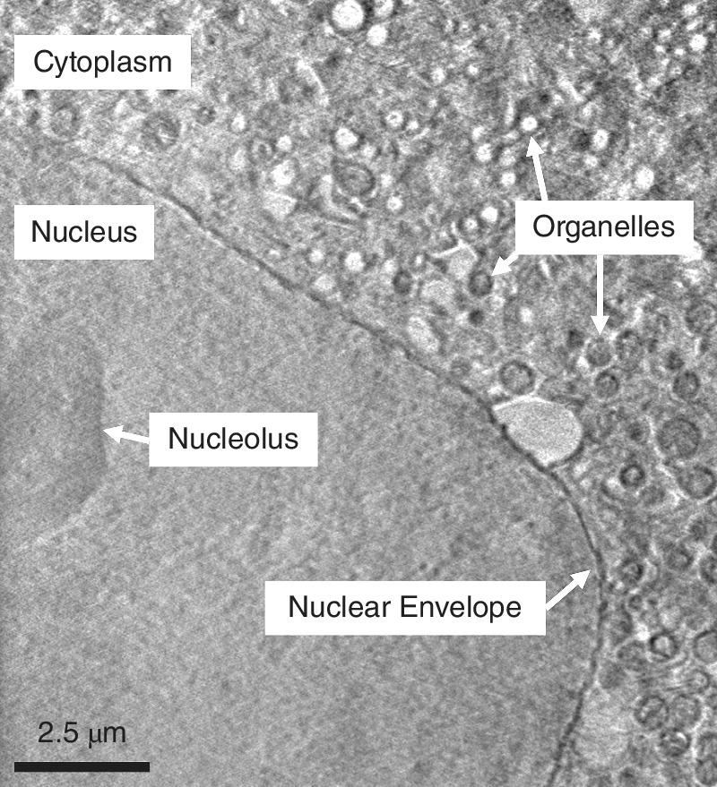
Figure 4.39 Slice of a three‐dimensional construct of a neuron‐like mammalian cell taken by cryogenic full field transmission x‐ray microscopy using 500 eV radiation.
(Source: Courtesy of Elizabeth Duke and Michele Darrow)
This technique can be used at higher x‐ray energies, and this will allow less thin samples to be used for inorganic materials. Elemental maps can be obtained by comparing images before and after an absorption edge, and XANES spectra derived by careful treatment of images recorded with different x‐ray energies near an absorption edge of interest.[28] Care must be taken due to the chromatic nature of the diffraction imaging of a zone plate and also the change in background absorption of the sample.
4.4.3 X‐Ray Photoelectron Emission Microscopy (X‐PEEM)
A very different full‐field approach involves use of an electron microscope to capture images from photoelectrons emitted the sample surface under the x‐ray beam. Typically this is employed in the soft x‐ray region (< 2000 eV), a fertile region for studying magnetic properties using the L edges of 3d elements. The ultra‐high vacuum conditions preferred of optimizing the electron microscope are consonant with the high absorption coefficients of samples in this energy regime and also on the need for surface cleanliness for what is a surface‐selective technique. Spatial resolutions of 20–30 nm can be achieved. By using XMCD methods, magnetic domains can be imaged using this method, as illustrated for a film of La0.7Ca0.3MnO3 on BaTiO3 (Figure 4.40). This material displays a giant magnetocalorific effect close to temperature (~200 K) of a phase change of the BaTiO3 substrate.[29] The image is based on the Mn XMCD contrast measured using the Mn L3 (~640 eV) and L2 (~650 V) edges, and shows different orientations of magnetic moments of Mn in the domains.
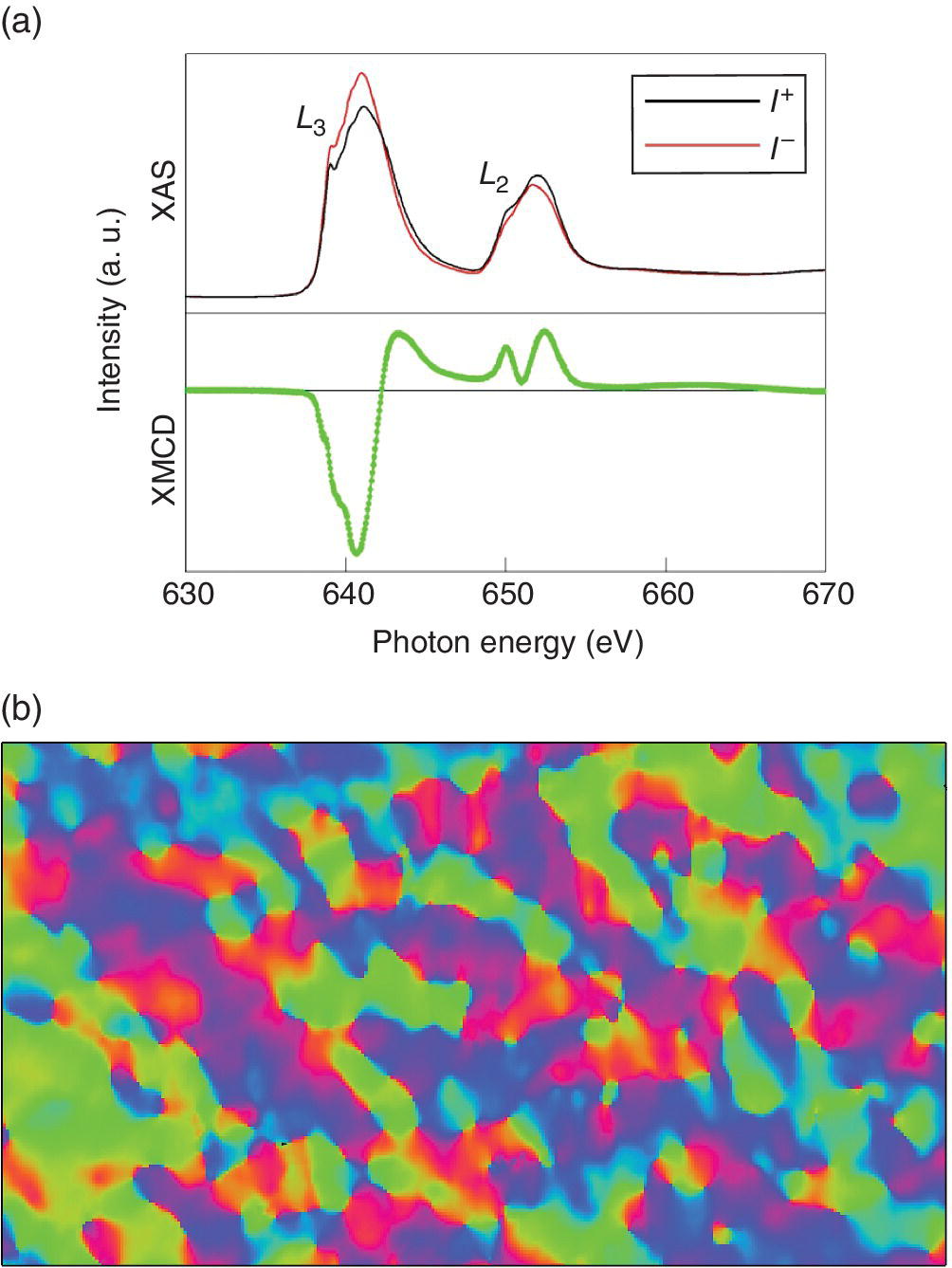
Figure 4.40 a) XAFS with right (I+) and left (I−) circular polarization and electron yield detection and the resulting XMCD signal of the Mn L2/3 edges of La0.7Ca0.3MnO3 on BaTiO3 at 210K and an applied magnetic field of 0.5. b) A zero field Mn PEEM image at ~150 K; image resolution 50 nm.
(Source: Courtesy of Sarnjeet Dhesi)
4.4.4 Focused‐Beam Microscopies
The alternative approach to imaging is to raster the sample against a highly focused x‐ray beam. In principle, the effects of the x‐rays on the sample can be measured by all the XAFS techniques described in Section 4.3, and also by x‐ray diffraction.
4.4.4.1 Scanning Micro‐ and Nano‐Focus Microscopy
An example schematic for a microfocus spectroscopy beamline, I18 at Diamond, is shown in Figure 3.4. Medium energy monochromatic light is focused onto the secondary slits, which act as the source for the second stage of focusing using Kirkpatrick‐Baez (KB) mirrors (Section 3.3.3.1). The result is a beam size of the order of 1 µm. An elemental map of the sample can be built up using the output of the MCA of an energy‐selective fluorescence detector to estimate the elemental content at each pixel. These measurements are stored with the array of positional data as the x‐ray beam is rastered over the sample; a spatial map can be constructed from these files. Oxidation state maps may be derived from measurements at particular energies within the XANES region. Additionally, XAFS spectra may be recorded at regions of importance within the sample. An example of how this is used to speciate a textured sample is shown in Figure 4.41. The sample is a sliver of wood (Figure 4.41a) taken from the Henry VIII’s warship, the Mary Rose. The ship sank in 1545 after being in service for 34 years, and was raised from the bed of the Solent in 1982. Since then there has been a major conservation project emanating from the museum in Portsmouth. The sulfur fluorescence maps (Figure 4.41b) show a low proportion of reduced sulfur, with the majority of the element being in the form of sulfate(VI). The maps of Fe fluorescence display a very small proportion of Fe(II), with the majority of the iron being present as Fe(III) (Figure 4.41c). The elements occupy very similar regions of the sample, and it is considered that iron is associated the oxidation of organic sulfur to sulfate. This results in highly corrosive localities, and conservation is designed to mitigate this.[30]
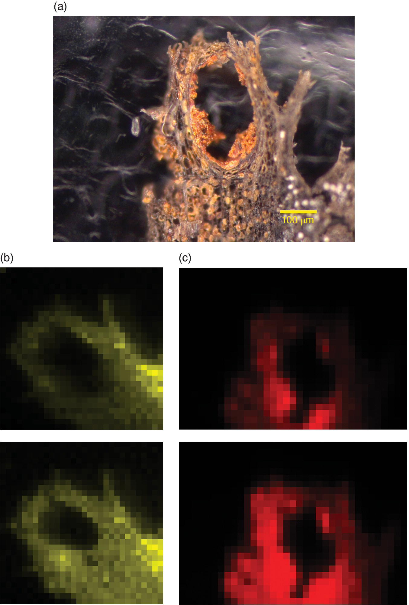
Figure 4.41 Images of a sliver of wood from the Tudor warship Mary Rose. a) Optical image. b) Sulfur fluorescence map with excitation at 2473.1 eV (upper) and above 2482.1 eV (lower). c) Fe fluorescence map of Fe(II) (upper, amplified 4X) and total Fe (lower).
(Source: Courtesy of Andy Smith, University of Manchester)
The spatial resolution can be enhanced by increasing the ratio of the distances between the secondary source and the focusing elements and the focusing element to the sample. In practice this requires a long beamline, as in I14 of the Diamond (Figure 4.42). Substitution of the KB mirrors by a zone plate will further reduce the beam size to the order of 10 nm, but this probably restricts the viable energy range of XAFS scans (see Section 3.3.3.3).
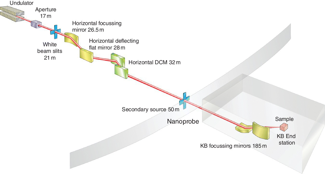
Figure 4.42 Schematic of the initial layout for beamline I14 at Diamond.
4.4.4.2 Scanning (Transmission) X‐Ray Microscopy (STXM)
A scanning transmission x‐ray schematic is presented in Figure 4.43, for beamline I08 at Diamond. Typically for a STXM, this beamline is based upon an undulator source, with a high degree of coherence. The coherence is required to give optimum resolution from the focusing zone plate.[31] The sample stage is rastered against the x‐ray beam (250–4200 eV) and an absorption contrast image can be recorded on the CCD camera with a resolution of ~20 nm. Phase‐contrast imaging may also be performed. At each point in the sample position a XANES spectrum can be measured, and a map of constituents in the sample can be constructed post‐acquisition using XANES features. As for the medium energy micro‐ and nano‐focus beamlines, an energy selective fluorescence detector allows for element mapping. This particular beamline has a helical undulator as it source, and thus offers an alternative technique to X‐PEEM for investigating magnetic materials.
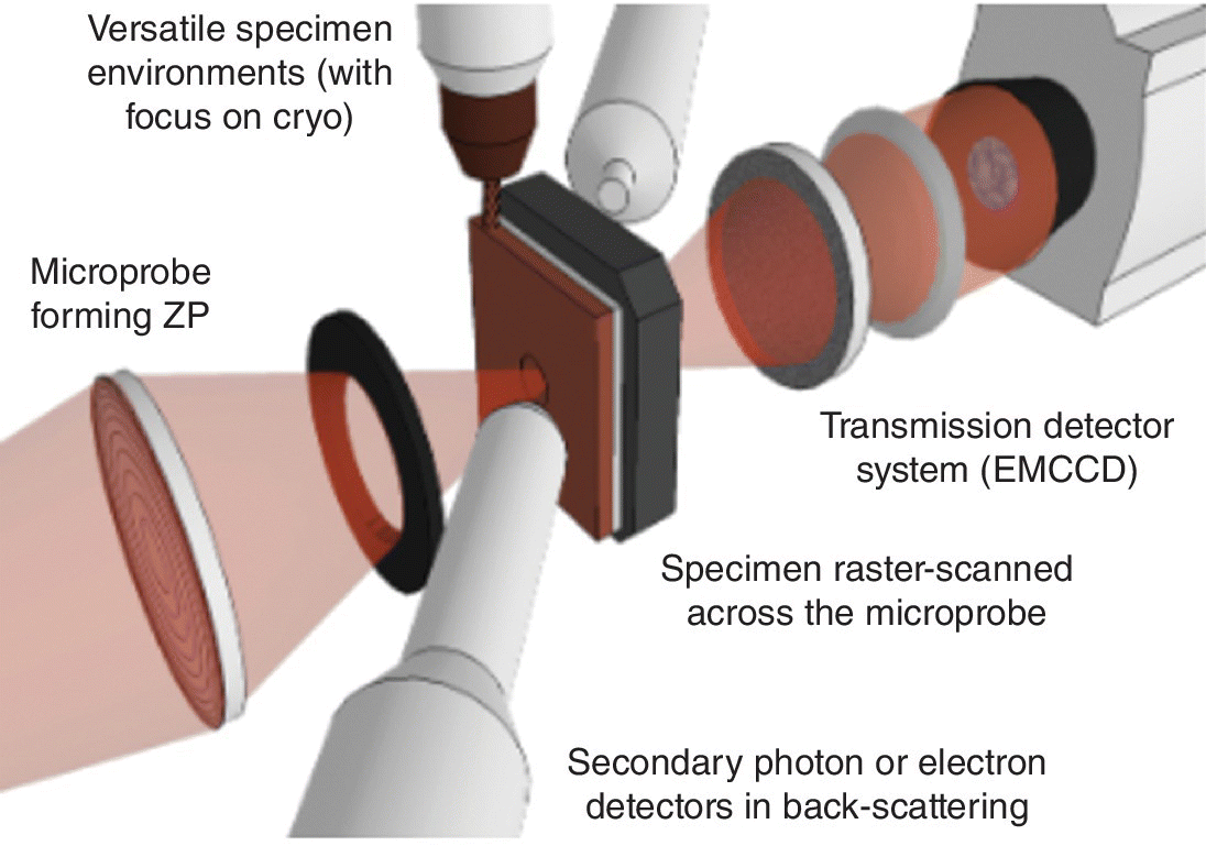
Figure 4.43 Schematic of the sample area of a scanning x‐ray microscope.
(Source: Diamond, I08)
An illustration of a materials application is the structural characterization of a sol‐gel derived silicon nitride sample with high surface area[32] (Figure 4.44). Micron‐sized particles are evident, which are uniform in terms of the silicon environment. The Si XANES spectrum is consistent with an environment like Si3N4 with negligible hydrolysis to silica.
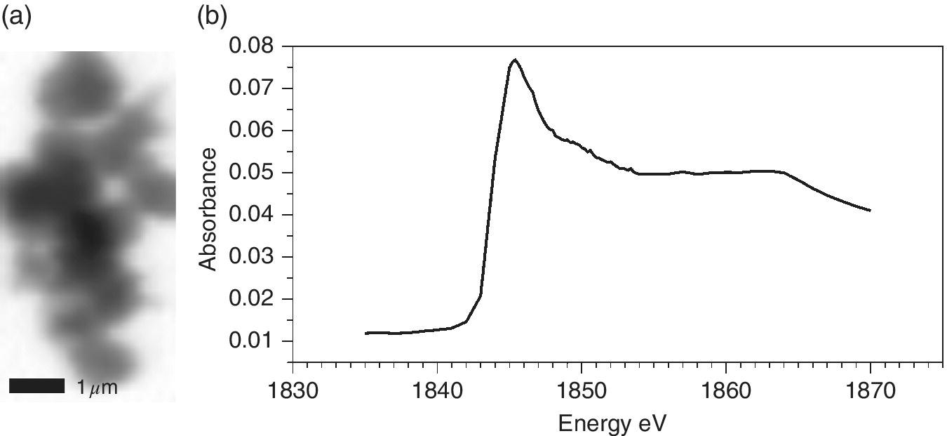

Figure 4.44 a) Absorption contrast image of a sol‐gel product from the reaction of Si(NHMe)4 with NH3 observed above the silicon K‐edge (1850 eV). b) Si K edge XANES of the imaged particle.
(Source: Courtesy of Andrew Hector, University of Southampton)
4.5 Combining Techniques
Many secondary techniques, such as uv‐visible, infra‐red, and Raman spectroscopies can be incorporated into the sampling area, providing that care is taken to match the sampling criteria for both that and the XAFS measurements. These are varied and some examples are provided in Chapter 6. In this chapter we concentrate on the main techniques also probed by the x‐radiation of the beamline.
4.5.1 Two‐Color XAFS
One aspect of this is to investigate a sample by acquiring spectra from more than one absorption edge. Monochromator and mirror settings can be stored and routines scripted to allow a sequence of edges to be studied. This can be achieved rapidly providing there are no changes in mirror or monochromator. If the sample is stable enough to allow this change then this is entirely viable. The sample concentration or thickness will not be optimized for each edge, but a compromise may well be feasible.
A slightly more sophisticated approach is to carry out a double‐edge study using the energy dispersive method (Section 4.2.2) with sufficiently large band spread as to span the XAFS range of two edges. Unlike the previous example, this type of measurement is genuinely synchronous and thus can be used for unstable systems and chemical change. An early example was the monitoring of the formation of platinum‐germanium catalyst particles from organometallic precursors;[33] the Pt L3 (11564 eV) and Ge K (11103 eV) are close enough to make both accessible but separated enough for the contamination of the platinum‐edge spectrum by that of germanium to be substantial. As the energies of the absorption edges are increased, the Bragg angle difference required to span a particular energy range is reduced. So it proved possible to obtain EXAFS for both the Rh (23220 eV) and Pd (24350 eV) K edges using a Si(111) polychromator[34] to during an in situ catalysis study of the reduction of NO.
Investigation of a sample using both hard and soft x‐ray energies would need two independent optical paths suitable for each energy range. This could be achieved with a split take‐off from a bending magnet, but a higher specification would by achieved with two different undulators with widely different characteristics. An example of this approach is Beamline I09 at Diamond (Figure 4.45). The line has the two undulators in an 8‐m‐long straight section, and these are canted so that the two beams may be separated into their own optical systems. These are recombined onto the sample within a UHV environment. A hemispherical electron energy analyzer enables hard x‐ray photoelectron spectroscopy (HAXPES) and XAS spectra to be recorded by, for example, total electron yield (Section 4.3.2). This can be illustrated with application as part of a major study into safer lithium ion cathodes following lithium ion doping into the phase ε‐LiVOPO4.[35] The O K edge XANES was sensitive to the degree of additional lithium incorporation due to the accompanying reduction of vanadium affecting the V‐O states.
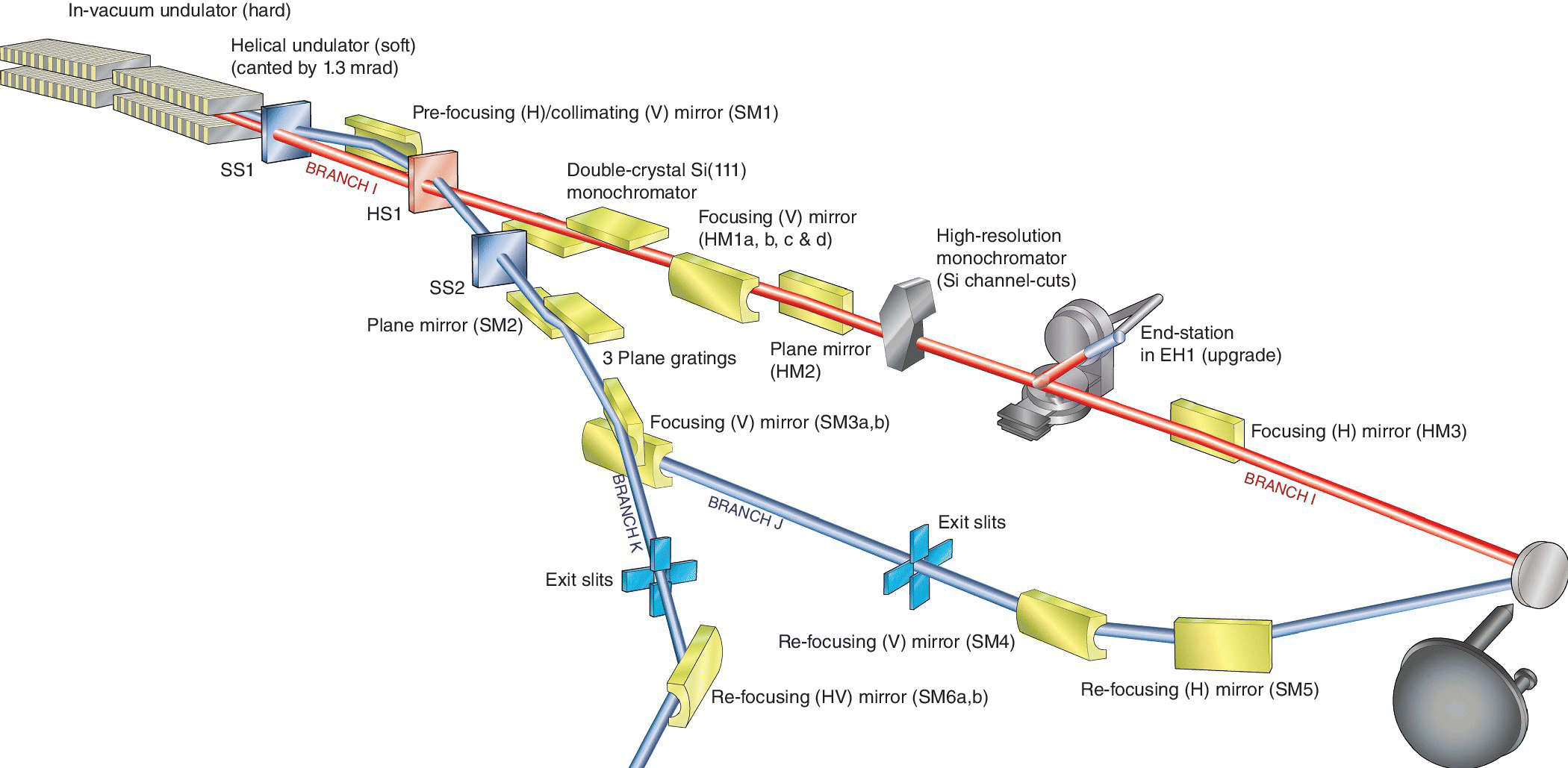
Figure 4.45 Schematic of beamline I09 at Diamond.
4.5.2 X‐Ray Scattering
A clear complementarity is achieved by incorporating x‐ray diffraction into an experimental setup, as illustrated in Figure 4.46. The sample position is at the center of the circle containing the arc of the detector. Generally, XAFS spectra and powder diffraction patterns are taken successively, with the monochromator driven quickly to the energy of choice for the diffraction measurements. Providing the lifetime of the sample is at least of the order of minutes, the two techniques will be measuring the same sample. However, they may not equally probe the same components of a textured sample. The diffraction pattern will be dominated by components with a large mosaic providing a sharp, intense diffraction lines; the XAFS spectra will monitor the mean of the sites of the absorbing element, although for XAFS too, the sites of highest local order will provide the more evident backscattering. An optimal case for complementarity is a solid solution. The diffraction pattern will afford the long‐range order with disordered occupancy of the lattice sites. XAFS measured for the component elements will reveal the distinct interatomic distances local to each element. In such circumstances both the diffraction and EXAFS results can be advantageously combined into a linked refinement procedure.[36]
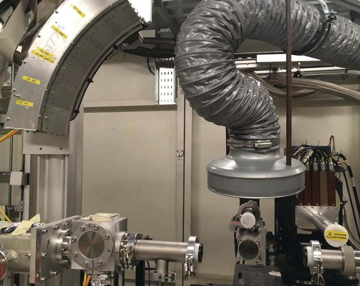
Figure 4.46 Installation of a curved multi‐element solid‐state detector for wide‐angle x‐ray scattering on an XAFS beamline.
(Source: Diamond, B18)
4.6 X‐Ray Free Electron Lasers (XFELs)
The number of stations equipped to carry out XAFS measurements at XFELs will increase significantly in 2017. Such experiments require their own sampling arrangements that are more stringent than those at synchrotron sources. They can extend the scope of XAFS studies into the fundamentals of processes.[37] In one sense, XFELs provide a level playing field. It is not the case that only tender, biological samples will suffer radiation damage; every sample must be considered tender and effectively one‐shot sampling must be devised. Care of the effects on the exposed single‐shot sample need also be taken. One of the benefits of having x‐ray pulses of the order of 10 fs is that x‐ray scattering takes place sufficiently fast that is can be measured before the sample undergoes a coulombic explosion; that is, when the sample area experiences a massive degree of ionization and the resultant charges repel and shoot away from each other. But the x‐ray flux can be such that it may violate the model of a single photon exciting an atom and the resulting excited state being observed by XAFS methods.
4.6.1 Laser‐Pump Measurements
The basic time sequence of a pump‐probe experiment is shown in Figure 4.47. Initiation of the change is effected by a laser pulse, and the sample can be probed by the x‐ray pulse after a possible delay period. In a synchrotron experiment this probe period can build up a time sequence of XAFS spectra, but this may be much more restricted in a FEL. There is a necessity to refresh the sample so that the next pulse interrogates the starting material. This pump‐probe combination is set within cycles without the pump laser to derive a background. XAFS difference spectra between the light‐on and light‐off periods are generally analyzed. The excitation energy provided by the laser pump is most commonly in the uv‐visible range. That is chosen to cause a specific photophysical transition within the lifetime of the pulse (~20 fs). The structural and electronic changes within the sample are then probed by XAFS. There will be a cascade of secondary photo‐physical and ‐chemical events dissipating this energy that may extend across several orders of magnitude of time units. In a solution or a solid matrix, this will end with local heating of the sample. Covering all of these events will involve experiments both at synchrotron and FEL sources. Alternative mechanisms for a pump source are i) to provide a heating pulse, for example into the electron sea of a metallic particle and ii) to excite a specific vibration within the sample in a multiphoton manner.
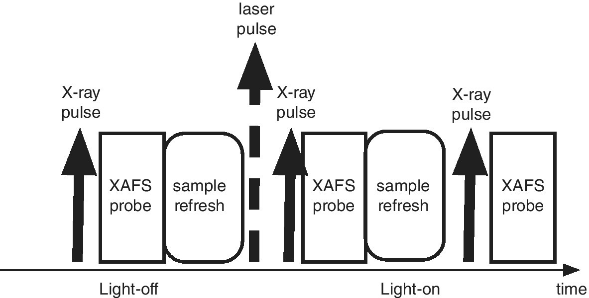
Figure 4.47 Schematic time sequence for a laser‐pump, XAFS‐probe experiment.
4.6.2 Sampling Environments
The intense energy sources of both pump and probe have consequences for the sampling methods. Our initial pump‐probe solution experiments at synchrotron sources stumbled over several of these![38] We utilized highly unsymmetrical effective path lengths for transmission XAFS (~3 mm with pyrolytic carbon windows) and the laser excitation (sampled with a x‐ray horizontal beam size of 5 µm). The recirculating solution was in contact with the surface of a quartz waveguide for the incoming laser. The build up of material on the surface of the quartz windows would result in increased energy absorption and fracturing of the ends of the waveguides. A subsequent experiment, also at ID24 of the ESRF, attempted to overcome this by recirculating the sample through a quartz capillary, which was translated during the experiment. Both the exciting laser and the polychromatic x‐ray beam each caused deposition on the capillary and thus the spectra were contaminated by those of the decomposition product.
The preferred sampling arrangement for solutions avoids contact between the sample and the x‐ray and laser windows.[39] The recirculating system is maintained but includes a liquid jet within the laser beam. The x‐ray probe beam is positioned inside the excited portion of the jet. This is illustrated in Figure 4.48 in the installation at the SuperXAS beamline (SLS). The liquid jet can be seen inside an environmental chamber sitting in front of the fluorescence detection system consisting of a filter foil, Soller slits. and APD detector.
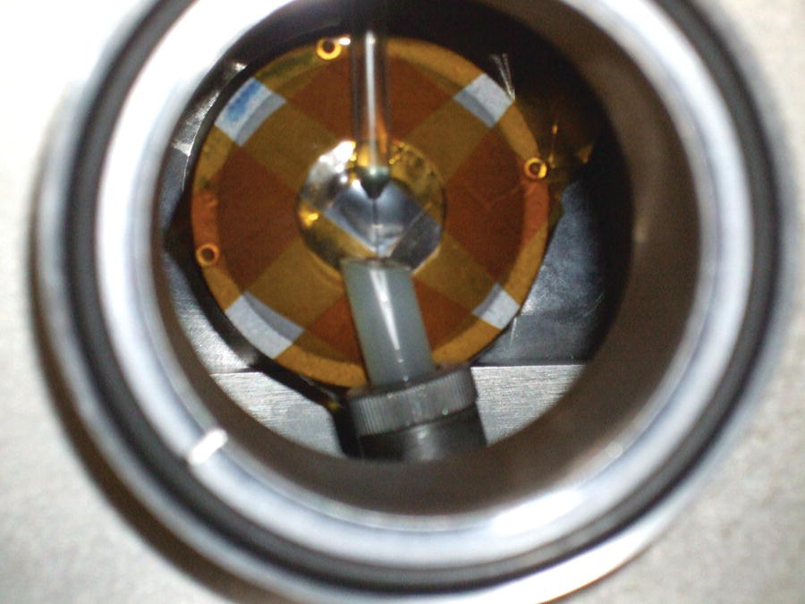
Figure 4.48 Liquid jet sampling system for time‐resolved XAFS (SLS, X10DA).
For most other studies, windowless sampling has been chosen. Trains of protein crystals are delivered from a jet in a viscous liquid, and these may be mixed with reagent solutions via concentric glass capillaries to allow time‐resolved crystallography of the products.[40] Similarly, a W L3 XAFS study of WO3 nanoparticles was carried out flowing a suspension.[41] Typical in situ heterogeneous catalysis studies within microreactors may have to be rethought. The suspension method may provide a route for liquid‐solid systems or for those systems in which the active gaseous reagent is highly soluble. Gas‐solid environments may possibly be investigated using thin or sputtered films on a sample belt.
4.6.3 X‐Ray Beam Intensity
The high intensity can cause multiple ionizations of the absorbing atom, as has been reported for H2S;[42] each sulfur atom absorbed an average of five photons. This situation is rather outside that of normal XAFS theory. This intensity can also result in non‐linear effects like frequency‐doubling, as has been reported for a germanium sample[43] using a highly focused beam to increase the flux density.
4.6.4 XAS and XES
But experimental conditions have been derived that are viable for XAFS studies.[44] A pump‐probe study of the photophysics of [Ni(TMP)] (TMP = tetramesitylphorphyrin) utilized x‐ray fluorescence detection at the Ni K edge to track the first ps of the cascade of processes;[45] a similar approach has been adopted to investigate [Fe(bipy)3]2+.[39] The instrument at LCLS also includes XES,[44] as has been used to investigate the manganese sites in photosystem II.[46] One of these systems is based upon the van Hamos geometry for a dispersive emission spectrometer (Figure 4.49).[47,48] This has the advantage over a Johann geometry in that an emission spectrum can be dispersed across the position sensitive detector (Figure 4.25). Thus one of the two dimensions of a RIXS plane is measured simultaneously, so dramatically reducing the number of measurements that need be made. This is of considerable benefit in time‐resolved studies. There are complications however. As the Bragg angle changes across the image of the XES pattern, the resolution will also change across it. Also the solid angle collected for each energy point is very low, and so it is difficult to match the sensitivity and resolution of the Johann geometry. However, with a FEL source the pulse flux is extremely high and the van Hamos arrangement is proving to be very productive. [44,46]
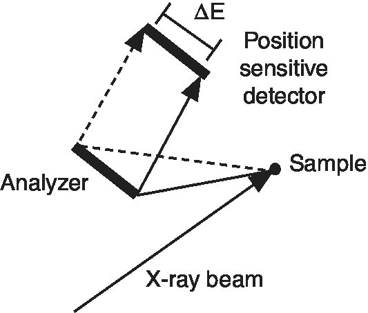
Figure 4.49 Schematic of a van Hamos geometry for an energy‐dispersive x‐ray emission spectrometer.
4.7 Questions
- 1 One method of the neutralization of chlorine bleach, NaOCl, is to treat it with sodium thiosulfate, Na2S2O3. You are assessing how to study this reaction in situ by XAFS since both chlorine and sulfur change oxidation states.
- What are the attenuation lengths of an aqueous solution at the viable edges of these two elements?
- What are the attenuation lengths of air at these energies?
- What would be the transmission of a 25 micron film of a polyester window at these energies {Consider the polyester as (‐C2H4CO2C6H4CO2‐)n}?
- Sketch a sampling system that could be successful for this experiment, giving your reasons.
- 2 Your project involves the synthesis of small particles of what you consider is Fe3O4. You synthesized this from a metallorganic, [Fe(acac)3], dissolved in ethanol, and then deposited the Fe3O4 onto a selection of supports, and are considering how to study the structure and properties of the iron.
- The precursor solution has a concentration of Fe of 20 mM. Calculate the transmission of the sample before and after the Fe K edge for path lengths of 1 mm and 5 mm and the resulting edge jump. What path length would you propose to carry out a transmission measurement?
- You have deposited the iron onto high area silica, SiO2, at a concentration of 5 wt% and have made a pressed disc (density 1 gcm−3) with a thickness of 200 µm. Calculate the transmission and edge jump of this sample. How would you propose to carry out this measurement? You are interested in the degree of crystallinity of this sample. How might you investigate that?
- You have also deposited your sample onto the surface of a quartz crystal wafer. How might you investigate the structure and shape of the particles? How could you investigate their magnetic properties?
- 3 Another sample was prepared starting from [Al(acac)3], which you believe forms a colloidal material in aqueous ethanol. Subsequently you make similar supported samples.
- How might you image the colloidal material in the aqueous medium?
- You are interested in how the aluminum is distributed in the supported material. Design an experiment to investigate this.
- 4 You have a sample from a mining process and need to understand the environment of the minerals within the sample to optimize the next step in the process. The material has a clay base (aluminosilicate) and is believed to contain nickel, rhodium, silver, palladium, platinum, and gold. Upstream in the process had been a treatment with HCl. Your group is considering purchasing beam time on a line with an energy range of 2–12 keV fitted with an energy‐resolving fluorescence detector based on silicon diodes with a multichannel analyzer with a quoted energy resolution of 150 eV at 5.9 keV.
- Assess the effectiveness of x‐ray fluorescence mapping in examining the distribution of these elements across the sample?
- In this mixture which absorption edges would be used to characterize the materials by XANES?
- Which of these might be viable for an EXAFS analysis?
- 5 You are designing time‐resolved experiments that will use an APD as a fluorescence detector and will need a filter before the detector to improve the signal/background ratio. By considering the energies of the absorption edges and main emissions,
- Propose a filter for an experiment at the vanadium K edge
- Consider the possibilities for studying the uranium L3 edge.
References
- 1 ‘A new flexible monochromator setup for quick scanning x‐ray absorption spectroscopy’, J. Stötzel, D. Lützenkirchen‐Hecht, R. Frahm, Rev. Sci. Instrum., 2010, 81, 073109.
- 2 ‘Advances in high brilliance energy dispersive x‐ray absorption spectroscopy’, S. Pascarelli, O. Mathon, Phys. Chem. Chem. Phys., 2010, 12, 5535–5546.
- 3 ‘Probing depth study of conversion electron/He ion yield XAFS spectroscopy on strontium titanate thin films’, E. Yanase, I. Watanabe, M. Harada, M. Takahashi, Y. Dake, Y Hiroshima, Anal. Sci., 1999, 15, 255–258.
- 4 ‘In situ studies of catalysts under reaction conditions by total electron yield XAS: possibilities and limitations of a new experimental technique’, S. L. M. Schroeder, G. D. Moggridge, E. Chabala, R. M. Ormerod, T. Rayment,R. M. Lambert, Faraday Discuss., 1996, 105, 317–336.
- 5 ‘Electron‐yield x‐ray absorption spectroscopy with gas microstrip detectors’, T. Rayment, S. L. M. Schroeder, G. D. Moggridge, J. E. Bateman, G. E. Derbyshire, R. Stephenson, Rev. Sci. Instrum., 2000, 71, 3640–3645.
- 6 ‘X‐ray fluorescence yields, Auger, and Costner‐Kronig transition probabilities’, W. Bambynek, B. Crasemann, R. W. Fink, H.‐U. Freund, H. Mark, C. D. Swift, R. E. Price, P. V. Rao, Rev. Modern Phys., 1972, 44, 716–813.
- 7 ‘Atomic radiative and radiationless yields for K‐shells and L‐shells’, M. O. Krause, J. Phys. Chem. Ref. Data, 1979, 8, 307–327.
- 8 ‘An x‐ray filter assembly for fluorescence EXAFS measurements’, E. A. Stern, S. M. Heald, Nucl. Instrum. Meth. 1980, 172, 397–399.
- 9 ‘Instrumentation for glancing angle x‐ray absorption spectroscopy on the Synchrotron Radiation Source’, S. Pizzini, K. J. Roberts, G. N. Greaves, N. Harris, P. Moore, E. Pantos, R. J. Oldman, Rev. Sci. Instrum., 1989, 60, 2525–2528.
- 10 ‘A high‐resolution x‐ray fluorescence spectrometer for near‐edge absorption studies’, V. Stojanoff, K. Hämäläinen, D. P. Siddons, J. B. Hastings, L. E. Berman, S. Cramer, G. Smith, Rev. Sci. Instrum., 1992, 63, 1125–1127.
- 11 ‘Five element Johann‐type X‐ray emission spectrometer with a single‐photon‐counting pixel detector’, E. Kleymenov, J. A. van Bokhoven, C. David, P. Glatzel, M. Janousch, R. Alonso‐Mori, M. Studer, M. Willimann, A. Bergamaschi, B. Henrich, M. Nachtegaal, Rev. Sci. Instrum., 2011, 82, 065107.
- 12 ‘A seven‐crystal Johann‐type hard x‐ray spectrometer at the Stanford Synchrotron Radiation Source’, D. Sokaras, T.‐C. Weng, D. Nordlund, R. Alonso‐Mori, P. Velikov, D. Wenger, A. Garachtchenko, M. George, V. Borzenets, B. Johnson, T. Rabedeau, U. Bergmann, Rev. Sci. Instrum., 2013, 84, 053102.
- 13 K. Hämäläinen, D. P. Siddons, J. B. Hastings, L. E. Berman, ‘Elimination of the inner‐shell lifetime broadening in x‐ray absorption spectroscopy’, Phys. Rev. Lett., 1991, 67, 2850–2853.
- 14 ‘Natural widths of atomic K and L levels, Kα x‐ray lines and several KLL Auger lines’, M. O. Krause, J. H. Oliver, J. Phys. Chem. Ref. Data, 1979, 8, 329–338.
- 15 ‘Appendix B. Core‐hole lifetime broadening’ in ‘Unoccupied electronic states. Fundamentals of XANES, EELS, IPS and BIS’, Ed. J. C. Fuggle, J. E. Inglesfield, Springer Verlag, Berlin, 1992.
- 16 ‘X‐ray resonant Raman scattering: observation of characteristic radiation narrower than the lifetime width’, P. Eisenberger, P. M. Platzman, H. Winick, Phys. Rev. Lett., 1976, 36, 623–626.
- 17 ‘Core level spectroscopy of solids’, F. de Groot, A. Kotani, CRC Press, 2008, Boca Raton.
- 18 ‘High resolution 1s core hole x‐ray spectroscopy in 3d transition metal complexes – electronic and structural information’, P. Glatzel, U. Bergmann, Coord. Chem. Rev., 2005, 249, 65–95.
- 19 ‘X‐ray Raman scattering. Experiment I’, T. Suzuki, J. Phys. Soc. Japan, 1967, 22, 1139–1150.
- 20 ‘X‐ray Raman scattering as a substitute for soft‐x‐ray extended‐x‐ray‐absorption fine structure’, K. Tohji, Y. Udagawa, Phys. Rev. B, 1989, 39, 7590–7594.
- 21 a’ Mulitelement spectrometer for efficient measurement of the momentum transfer dependence of inelastic x‐ray scattering’, T. T. Fister, G. T. Seidler, L. Wharton, A. R. Battle, T. B. Ellis, J. O. Cross, A. T. Macrander, W. T. Elam, T. A. Tyson, Q. Qian, Rev. Sci. Instrum., 2006, 77, 063901; b‘A high resolution and large solid angle x‐ray Raman spectroscopy end‐station at the Stanford Synchrotron Radiation Lightsource’, D. Sokaras, D. Nordlund, T.‐C. Weng, R. Alonso Mori, P. Velikov, D. Wenger, A. Garachtchenko, M. George, V. Borzenets, B. Johnson, Q. Qian, T. Rabedeau, U. Bergmann, Rev. Sci. Instrum., 2012, 83, 043112; c‘A large‐solid‐angle x‐ray Raman scattering spectrometer at ID20 of the European Synchrotron Radiation Facility’, S. Huotari, Ch. J. Sahle, Ch. Henriquet, A. Al‐Zein, K. Martel, L. Simonelli, R. Verbeni, H. Gonzalez, M.‐C. Lagier, C. Ponchut, M. Moretti Sala, M. Krisch, G. Monaco, J. Synchrotron Radiat., 2017, 24, 521–530.
- 22 ‘Bulk‐sensitive characterization of the discharged products in Li‐O2 batteries by nonresonant inelastic x‐ray scattering’, N. K. Karan, M. Balasubramanian, T. T. Fister, A. K. Burrell, P. Du, J. Phys. Chem. C, 2012, 116, 18132–18138.
- 23 ‘X‐ray excited optical luminescence (XEOL) detection of x‐ray absorption fine structure (XAFS)’, L. Soderholm, G. K. Liu, M. R. Antonio, F. W. Lytle, J. Chem. Phys., 1998, 109, 6745–6752.
- 24 ‘Synchrotron radiation x‐ray excited optical luminescence for chemical state selective analysis’, S. Hayakawa, T. Hirose, L. Yan, M. Morishita, H. Kuwano, Y. Gohshi, X‐ray Spectrom., 1999, 28. 515–518.
- 25 ‘A time resolved microfocus XEOL facility at the Diamond Light Source’, J. F. W. Mosselmans, R. P. Taylor, P. D. Quinn. A. A. Finch, G. Cibin, D. Gianolio, A. V. Sapelkin, J. Phys. Conf. Ser., 2013, 425, 182009.
- 26 ‘OD‐XAS and EXAFS: Structure and luminescence in Ge quantum dots’, A. Karatutlu, W. R. Little, A. V. Sapelkin, A. Dent, F. Mosselmans, G. Cibin, R. Taylor, J. Phys. Conf. Ser., 2013, 430, 012026.
- 27 ‘Biological applications of cryo‐soft x‐ray tomography, E. Duke, K. Dent, M. Razi, L. M. Collinson, J. Microsc., 2014, 255, 65–70.
- 28 ‘Three‐dimensional imaging of chemical phase transformations at the nanoscale with full‐field transmission x‐ray microscopy’, F. Meirer, J. Cabana, Y. Liu, A. Mehta, J. C. Andrews, P. Pianetta, J. Synchrotron Radiat., 2011, 18, 773–781.
- 29 ‘Giant and reversible extrinsic magnetocaloric effects in La0.7Ca0.3MnO3 films due to strain’, X. Moya, L. E. Hueso, F. Maccherozzi, A. I. Tovstolytkin, D. I. Podyalovskii, C. Ducati, L. C. Phillips, M. Ghidini, O. Hovorka, A. Berger, M. E. Vickers, E. Defray, S. S. Dhesi, N. D. Mathur, Nature Mater., 2013, 12, 52–58.
- 30 ‘The application of x‐ray absorption spectroscopy in archaeological conservation: Example of an artifact from Henry VIII warship, the Mary Rose’, A. V. Chadwick, A. Berko, E. J. Schofield, A. D. Smith, J. F. W. Mosselmans, A. M. Jones, G. Cibin, J. Non‐Crystalline Solids, 2016, 451, 49–55.
- 31 ‘Illumination for coherent soft x‐ray applications: the new X1A beamline at the NSLS’, B. Winn, H. Ade, C. Buckley, M. Feser, M. Howells, S. Hulbert, C. Jacobsen, K. Kaznacheyev, J. Kirz, A. Osanna, J. Maser, I. McNulty, J. Miao, T. Oversluizen, S. Spector, B. Sullivan, Y. Wang, S. Wirick, H. Zhang, J. Synchrotron Radiat., 2000, 7, 395–404.
- 32 ‘Sol‐gel preparation of low oxygen content, high surface area silicon nitride and imidonitride materials’, K. Sardar, R. Bounds, M. Caravetta, G. Cutts, J. S. J. Hargreaves, A. L. Hector, J. A. Hriljac, W. Levason, F. Wilson, Dalton Trans., 2016, 45, 5765–5774.
- 33 ‘In situ, time resolved and simultaneous multi‐edge determination of local order change during reduction of supported bimetallic (Pt‐Ge) catalyst precursors using energy dispersive EXAFS’, S. G. Fiddy, M. A. Newton, T. Campbell, J. M. Corker, A. J. Dent, I. Harvey, G. Salvini, S. Turin, J. Evans, Chem. Comm., 2001, 445–446.
- 34 ‘The impact of phase changes, alloying and segregation in supported RhPd catalysts during selective NO reduction by H2’, M. A. Newton, B. Jyoti, A. J. Dent, S. Diaz‐Moreno, S. G. Fiddy, J. Evans, ChemPhysChem, 2004, 5, 1056–1058.
- 35 ‘Uniform second Li ion intercalation in solid state ε‐LiVOPO4’, L. W. Wangoh, S. Sallis, K. M. Wiaderek, Y.‐C. Lin, B. Wen, N. F. Quackenbush, N. A. Chernova, J. Guo, L. Ma, T. Wu, T.‐L. Lee, C. Schlueter, S. P. Ong, K. W. Chapman, M. S. Whittingham, L. F. J. Piper, Appl. Phys. Lett., 2016, 109, 053904.
- 36 ‘Combined EXAFS and powder diffraction analysis’, N. Binsted, M. J. Pack, M. T. Weller, J. Evans, J. Am. Chem. Soc., 1996, 118, 11200–11210.
- 37 ‘Dynamic structure elucidation of chemical reactivity by laser pulses and X‐ray probes’, S. A. Bartlett, M. L. Hamilton, J. Evans, Dalton Trans., 2015, 44 6313–6319.
- 38 ‘Energy dispersive XAFS: Characterization of electronically excited states of copper(I) complexes’, M. Tromp, A. J. Dent. J. Headspith, T. L. Easun, X.‐Z. Sun, M. W. George, O. Mathon, G. Smolentsev, M. L. Hamilton, J. Evans, J. Phys. Chem. B, 2013, 117, 7381–7387.
- 39 ‘Femtosecond x‐ray absorption spectroscopy at a hard X‐ray free electron laser: application to spin crossover dynamics’, H. T. Lemke, C. Bressler, L. X. Chen, D. M. Fritz, K. J. Gaffney, A. Galler, W. Gawelda, K. Haldrup, R. W. Hartsock, H. Ihee, J. Kim, K. H. Kim, J. H. Lee, M. M. Nielsen, A. B. Stickrath, W. Zhang, D. Zhu, M. Cammarata, J. Phys. Chem. A, 2013, 117, 735–740.
- 40 ‘Mixing injector enables time‐resolved crystallography with high hit rate at X‐ray free electron lasers’, G. D. Calvey, A. M. Katz, C. B. Schaffer, L. Pollack, Struct. Dynamics, 2016, 3, 054301.
- 41 ‘Dynamics of photoelectrons and structural changes of tungsten trioxide by femtosecond transient XAFS’, Y. Uemura, D. Kido, Y. Wakisaka, H. Uehara, T. Ohba, Y. Niwa, S. Nozawa, T. Sato, K. Ichiyanagi, R. Fukaya, S.‐i. Adachi, T. Katayama, T. Togashi, S. Owada, K. Ogawa, M. Yabashi, K. Hatada, T. Takakusagi, T. Yokoyama, B. Ohtani, K. Asakura, Angew. Chem. Int. Ed., 2016, 55, 1364–1367.
- 42 ‘Multiphoton L‐shell ionization of H2S using intense x‐ray pulses from a free electron laser’, B. F. Murphy, L. Fang, M.‐H. Chen, J. D. Bozek, E. Kukk, E. P. Kanter, M. Messerschmidt, T. Osipov, N. Berrah, Phys. Rev. A, 2012, 86, 053423.
- 43 ‘X‐ray two‐photon absorption competing against single and sequential multiphoton processes’, K. Tamasaku, E. Shigemasa, Y. Inubushi, T. Katayama, K. Sawada, H. Yumoto, H. Ohashi, H. Mimura, M. Yabashi, K. Yamauchi, T. Ishikawa, Nat. Photonics, 2014, 8, 313–316.
- 44 ‘Photon‐in photon‐out hard X‐ray spectroscopy at the Linac Coherent Light Source’, R. Alonso‐Mori, D. Sokaras, D. Zhu, T. Kroll, M. Chollet, Y. Feng, J. M. Glownia, J. Kern, H. T. Lemke, D. Nordlund, A. Robert, M. Sikorski, S. Song, T.‐C. Weng, U. Bergmann, J. Synchrotron Radiat., 2015, 22, 612–620.
- 45 ‘Ultrafast excited state relaxation of a metalloporphyrin revealed by femtosecond x‐ray absorption spectroscopy’, M. L. Shelby, P. J. Lestrange, N. E. Jackson, K. Haldrup, M. W. Mara, A. B. Strickrath, D. Zhu, H. T. Lemke, M. Chollet, B. M. Hoffman, X. Li, L. X. Chen, J. Am. Chem. Soc., 2016, 138, 8752–8764.
- 46 ‘The Mn4Ca photosynthetic water‐oxidation catalyst studied by simultaneous x‐ray spectroscopy and crystallography using an x‐ray free‐electron laser’, R. Tran, J. Kern, J. Hattne, S. Koroidov, J. Hellmich, R. Alonso‐Mori, N. K. Sauter, U. Bergmann, J. Messinger, A. Zouni, J. Yano, V. K. Yachandra, Phil. Trans. R. Soc. B, 2014, 369, 20130324.
- 47 ‘A multi‐crystal wavelength‐dispersive x‐ray spectrometer’, R. Alonso‐Mori, J. Kern, D. Sokaras, T.‐C. Weng, D. Nordlund, R. Tran, P. Montanez, J. Delor, V. K. Yachandra, J. Yano, U. Bergmann, Rev. Sci. Instrum., 2012, 83, 073114.
- 48 ‘A von Hamos x‐ray spectrometer based on a segmented‐type diffraction crystal for single‐shot x‐ray emission spectroscopy and time‐resolved resonant inelastic scattering studies’, J. Szlatchetko, M. Nachtegaal, E. de Boni, M. Willimann, O. Safonova, J. Sa, G. Smolentsev, M. Szlatchetko, J. A. van Bokhoven, J.‐Cl. Dousse, J. Hoszowska, Y. Kayser, P. Jagodzinski, A. Bergamaschi, B. Schmitt, C. David, A. Lücke, Rev. Sci. Instrum., 2012, 83, 103105.


