Chapter 8
Instrumentation for Other Sensor Technologies
8.1 Chapter Overview
This chapter begins by detailing the reasons why temperature measurement is important for biosensing applications. It then describes methods for temperature sensing using resistive temperature detectors and silicon p-n junction diodes. These are considered to be the most relevant methods for temperature calibration of biosensors, particularly when microminiaturisation is required.
The second section of the chapter concentrates on different methods for mechanical sensing using three different modes of measurement: piezoresistive, piezoelectric, and capacitive sensing. Examples of applications in biosensing or biomedical measurement are included. The section on capacitive sensing leads naturally into an introduction to switched capacitor based instrumentation.
Fluorescent sensing is key to many biological and biomedical applications and the third part of this chapter will review the theory of fluorescence before describing photodetectors that can be used to transduce optical information into electrical signals. This section finishes with a discussion of a lab-on-a-chip biosensor which uses fluorescent readout and electrochemical actuation for detection of specific DNA sequences.
The final part of this chapter examines instrumentation for electrophysiology, and in particular the methods used to measure electrical activity in neurons. These techniques are extremely important for researchers attempting to understand the function of the nervous system and to develop treatments for neurological diseases.
After reading this chapter readers will gain a refreshed or new understanding of:
8.2 Temperature Sensors and Instrumentation
8.2.1 Temperature Calibration
One very important reason to integrate temperature measurements alongside other sensors is that in most cases there will be some cross-correlation between the output of a sensor and the temperature. This can be as simple as thermal variations in the value of a resistive sensor or the dependence of the chemical reactions in a biosensor on the ambient temperature. In addition some of the biological components of a biosensor system, such as enzymes, will often have a very narrow range of temperatures over which they operate. This means that the temperature sensors do not need to have a wide range but do need to be sensitive and accurate within this range.
Some common temperature sensors or instruments such as a glass thermometer or a bimetallic strip are not well suited to miniaturisation. In addition it is often useful to choose a transducer for temperature that is similar in nature to the sensor it will be used alongside. For example if the transduction method in a biosensor involves measuring a change in resistance it might be helpful if the temperature sensor is also resistive.
8.2.2 Resistance Temperature Detectors
Probably the most basic electrical or electronic temperature sensor is a simple resistive transducer which exploits the temperature dependence of the resistivity of most conductive materials. The basic formula for the resistance ( ) of a Resistance Temperature Detector (RTD) at a temperature
  is:
is:

This will depend on the resistance ( ) at some known calibration point
  . This is often 0 °C but it could simply be the midpoint of the temperature range of interest. The most important factor is the temperature coefficient
  which will depend on the resistor material and may be positive or negative. Metals in a solid state will generally have a positive coefficient of temperature. The units of
  are K−1.
One of the most common materials for RTDs is platinum and sensors made with this are usually referred to as platinum resistive thermometers or PRTs. Platinum is used because it is stable and proof against most contamination and corrosion that can affect the temperature coefficient, which will depend on the purity of the RTD material. Pt can be deposited in thin films and micromachined to produce narrow resistive tracks, for example on the surface of an integrated circuit. One standard type of PRT has a purity of platinum with a characteristic sensitivity of ~ 0.385 Ω K−1 when made into a resistor with a value of 100 Ω at 0 °C.
RTDs can be made as a thin film but a more common construction for a discrete sensor has a rigid former, made of a ceramic for example, around which a platinum wire is wound. More modern sensors may have coils of wire within a rigid, insulating support. The purpose of the former is mainly to support the wire and prevent the resistance of the RTD being altered by thermal expansion or other mechanical forces.
The variation of the resistance of a platinum RTD is not completely linear and a more complete description of the characteristic is given by the Callendar-Van Dusen equation, which comes in two forms depending on the temperature range being investigated:
(8.2) 
for temperatures −200 °C  0 °C and:
(8.3) 
for 0 °C  661 °C.
These equations contain higher order coefficients and these can be found by calibrating the individual resistor. The accepted values for a ‘pt100’ RTD with a standard temperature coefficient are:
Over the most typical temperature ranges the resistance is effectively linear and the 1st order equation (8.1) can be used with  K−1 and
  at 0 °C.
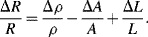
A common method to convert the resistance variation of an RTD sensor into a useful voltage signal is to place it into a Wheatstone bridge circuit (see Chapter 7, Section 7.7.1) as shown in Figure 8.1.
Figure 8.1 Resistive temperature detector in a Wheatstone bridge circuit.
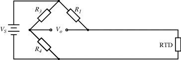
The variation in the output voltage  will be approximately proportional to the change in the resistance
  of the RTD. The main problem with this approach is that the resistances of the leads connecting the RTD are included in the measurement. That is not a significant issue when setting up the circuit, as the other resistors in the bridge can be tuned to balance the additional resistance of the leads. The problem arises when the sensor is used, as the lead resistance will also have some dependence on the temperature which will appear as an error in the temperature measurement if it varies significantly.
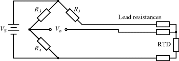
There are a number of different ways of compensating for the connection resistance. One of the most common methods involves using an extra lead to bring the output connection right down to where it connects to one side of the resistor (Figure 8.2). This lead should not carry much current unless the bridge is very unbalanced, and the outer resistances will cancel each other out in the bridge assuming the leads have well matched resistances. A more elaborate, 4-wire connection scheme adds a pair of dummy leads into the  section of the bridge (Figure 8.3) but this still depends on the leads being matched and is costly in terms of the amount of cabling required.
Figure 8.3 RTD bridge circuit with 4-wire compensation for connection resistance.
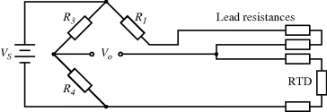
Figure 8.2 RTD bridge circuit with 3-wire compensation for connection resistance.
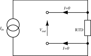
If accurate current sourcing and voltage measurement is available it is possible to do away with the bridge entirely and instead use a Kelvin or four-terminal measurement setup. Here the measurement current is forced through the resistive sensor while the voltage is measured with separate connections made as close as possible to the ends of the resistor (Figure 8.4). If the voltmeter has a high input impedance then little current will flow in these connections and the voltage measured will be solely due to the resistance of the sensor. This technique is named for Lord Kelvin (William Thompson) after his invention of the Kelvin or Thompson double bridge which applies a similar technique to the resistive Wheatstone bridge circuit.
Figure 8.4 Resistance temperature detector with four-terminal Kelvin measurement.
There are a number of important issues that need to be considered when using an RTD to measure temperature. Firstly, it is a passive sensor meaning that current needs to be supplied in order to make the measurement. If the current used is too high this can cause self-heating of the resistor and an error in the measurement. This implies that low currents are required but that will mean that there is a requirement to measure or amplify relatively small voltages. Secondly, the sensitivity of an RTD is the product of  and the temperature coefficient
  , suggesting that it might be useful to use a large value of resistance. Typically, a standard RTD sensor has
  at 0 °C but it may be possible when designing an integrated sensor to use a larger resistance. However, this would obviously be balanced by an increase in thermal noise from the RTD. Thirdly, all RTDs will have some sort of time constant reflecting how quickly they react to changes in the temperature of the measured environment. This will depend on the thermal conduction properties of the material of the resistor and of the packaging used. Heat sinks such as the wires connecting the RTD may also have an effect. Finally, the long-term stability of the sensor will depend on preventing contamination of the resistor material and avoiding strain gauge effects due to applied mechanical forces. The resistance to contamination or corrosion of platinum is one reason why it is chosen for this application.
Thermistors are similar to RTDs in that they are temperature dependent resistors but the difference is that they are usually not made from metal but from a conducting ceramic, polymer or semiconductor. Unlike metal RTDs they can have either a positive or negative thermal coefficient and can also have a non-linear response. For example, most semiconductors will have a negative thermal coefficient of resistance because heating will tend to increase the levels of free charge carriers. Thermistors with highly non-linear responses can be useful for application as temperature dependent switches.
8.2.3 p-n Junction Diode as a Temperature Sensor
Solid-state electronic temperature sensors represent an alternative solution for the measurement of temperature in integrated, microscale biosensing applications. The simplest method is to use a forward biased p-n junction diode as a sensor. Most readers should be somewhat familiar with the Shockley diode equation given below, which defines the current in the device as a function of the voltage bias,  , the reverse bias saturation current,
  , the temperature,
  , and some other physical constants:
(8.4) 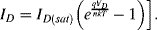
If, instead of applying a bias voltage a constant current is forced through the diode the equation can be rearranged to give the voltage across the diode, assuming that ID  ID(sat):
(8.5) 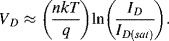
This appears at first glance to have a positive, linear dependence on temperature, due to the  in the term for the thermal voltage, but this does not take into account the temperature dependence of the saturation voltage
  . The overall effect of this is that the diode voltage is proportional to temperature with a sensitivity of about −2 mV K−1 for a typical silicon p-n junction.
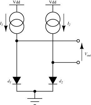
One disadvantage of the single diode as a sensor for temperature is that, although the sensitivity is well known, without calibration it is difficult to say what the temperature actually is. Small variations in the diode fabrication process can lead to significant variations in the saturation current. A differential measurement of two diodes with different currents can provide an absolute temperature measurement with a positive linear coefficient. If two different currents ( ,
,  ) are forced through two similar diodes as shown in Figure 8.5 the resulting difference in voltage drop across them is:
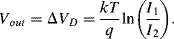
Equation (8.6) can be rearranged to give an expression for the absolute value of temperature in terms of the voltages, currents and physical parameters. The sensitivity of this system depends upon the ratio of the two currents, and a typical value for this is 10:1, which gives an overall sensitivity of 198 μV K−1. If the ratio of the currents is too high then significant errors can occur due to different levels of self-heating in the devices. It is also possible to take a single diode and alternately switch two different currents through it. The amplitude of the resulting ac voltage will have the same proportional to absolute temperature (PTAT) dependence as the circuit shown in Figure 8.5.
Figure 8.5 Proportional To Absolute Temperature (PTAT) sensor using p-n diodes.
The temperature dependences of silicon p-n junctions can be exploited to make a voltage reference circuit with an output that is insensitive to temperature. By combining parts with positive and negative temperature coefficients it is possible eliminate the temperature dependency. These circuits are often referred to as bandgap references because the output is set by the physical property of the silicon bandgap potential. Figure 8.6 shows an example of one standard voltage reference known as a Brokaw reference circuit [1]. The feedback loop made up from the operational amplifier and the other components will hold the voltages across the two equal resistances  and
and  equal so that the collector-emitter currents (
 ,
,  ) are the same in both transistors. The two transistors will have different emitter areas with a ratio of 10:1 so that the base emitter voltages, which depend on the current densities, will be different. These junction voltages (
 ,
,  ) will have a negative coefficient of temperature while the difference between
  and
and  (
( ) will have a positive coefficient as in the diode based temperature sensor. The voltage across
  will be:
Figure 8.6 Brokaw bandgap voltage reference circuit.
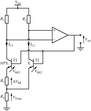
(8.7) 
where  and
and  are the current densities in the transistors. A temperature dependent voltage can be read out from the voltage across
  which is:
(8.8) 
The output voltage  . Careful choice of
  and
and  will balance the positive and negative temperature coefficients to give a constant output
  that is independent of temperature and is close to the bandgap voltage of silicon, typically around 1.25 V.
8.3 Mechanical Sensor Interfaces
This section will examine three different types of mechanical transduction with application in biosensing but it should be understood that there are a number of other modes of operation for micromechanical sensors and actuators, such as the use of magnetism. The three different transduction methods discussed here are:
8.3.1 Piezoresistive Effect
Piezoresistance is probably the simplest way to transduce movement into an electrical signal. It is a change in the resistance of a piece of material that is subjected to a mechanical force and was discovered by Lord Kelvin around 1856. It is also referred to as the strain gauge effect and most electrically readable strain gauges will operate in this way. It lends itself to microfabrication as thin film deposited or diffused resistors make good strain gauges. There is also a greater effect in semiconducting materials than there is in metallic conductors.
A typical strain gauge is fabricated in a thin metal layer on a flexible support, probably an insulating polymer. A typical design is illustrated in Figure 8.7 where the gauge will be sensitive to strain applied along the long axis of the structure. Stretching it in this direction will put the conducting material into tension, making it longer and thinner, and therefore increasing the resistance. Similarly putting it into compression, will make the conducting material shorter and wider in cross-section so that the resistance decreases.
Figure 8.7 Schematic design for a piezoresistive strain gauge.

A piezoresistive sensor is characterised by its gauge factor,  ; this is a dimensionless parameter defining the relative change in the resistance,
  , divided by the applied strain,
  :
:

The basic formula for resistance is  and from this is possible to define the fractional change in resistivity for a strain gauge:
The first term refers to the change in the material resistivity,  , due to the strain. The piezoresistive coefficient
  is defined as:
(8.11) 
where  is the Young's modulus of elasticity for the material and
  is the applied strain (
 ). Another important parameter is Poisson's ratio,
  , which defines the change in the transverse strain due to an applied axial strain. In most materials when they are stretched in one direction the cross sectional area will be reduced in the transverse directions and it is possible to define Poisson's ratio with this formula:

By combining Equations (8.10) to (8.12) with the expression for the gauge factor (8.9) it is possible to define  in terms of the material properties (
 ,
,  and
and  ):
):
In most metals the Poisson ratio is between 0 and 0.5 while the change in resistivity with strain is negligible. This means that the maximum GF for a typical metal strain gauge is ~ 2. With a good design strains of up to 10% can be measured but this requires a firm connection between the gauge and the structure being measured. For example, slippage in the glue used to stick down the gauge can reduce the coupling of strain and therefore the sensitivity.
The biggest issue to control in strain gauges is the effect of temperature as all materials used in strain gauges will have a resistivity that varies with temperature, as we have seen in Section 8.2.2. In addition there will be effects from thermal expansion of the gauge materials and this can add to the mechanical strain being measured. It is possible to make the gauge out of an alloy like constantan which has very low thermal coefficients of resistance and expansion.
There are a number of different ways to arrange strain gauges into a Wheatstone bridge, which can also serve to reduce temperature effects. The simplest is to replace two of the resistors in one side of the bridge with strain gauges but only one of the gauges should be fixed to the surface being measured. The other will be a dummy gauge that experiences the same thermal environment as the active strain gauge but does not change with applied force. The other two resistors should be chosen to have the same resistance of the unstrained gauges but may not be located near to the measurement. In an alternative setup is possible to use four gauges at the same time but arrange them so that two, opposite, gauges will be compressed, reducing  and two will be in tension, increasing
  . This gives a much larger imbalance to the bridge for the same input so the resulting output voltage sensitivity to strain will be maximised. This is illustrated in Figure 8.8 which will have an output voltage:
(8.14) 
Figure 8.8 Arrangement of strain gauges in a Wheatstone bridge circuit for maximum sensitivity.
It is very important to ensure that the gauges are properly arranged in the bridge circuit so that they do not cancel each other out and give no output at all. A mistake like this is the source of ‘Murphy's Law’ which is named for the US Airforce Engineer, Capt. Edward A. Murphy Jr. The full story of how this infamous law, which is often misstated as ‘If anything can go wrong it will’ but was originally ‘If it can happen, it will happen’, was coined is set out in [2, 3].
The piezoresistive effect is generally greater in semiconductors than in metals due to effects of strain on the mobility of charge carriers in the semiconductor. This means that the piezoresistive coefficient  dominates in Equation (8.13) resulting in gauge factors of 100 or more in single crystal silicon diffused resistors. The direction of the strain is very important in these devices as the value of
  will depend on the orientation of the crystal planes in these devices. Polysilicon piezoresistors will display less dependence on orientation but with the trade-off of a lower gauge factor. These mobility effects of strain are exploited in modern microelectronics. For example in advanced CMOS technologies the lattice mismatch between Si and SiGe is used to create strain in the channel region of transistors to improve the mobility.
8.3.2 Applications of Piezoresistive Sensing
Silicon or polysilicon strain gauges are ideal for integration into a MEMS sensor system and this section presents two examples with possible medical application.
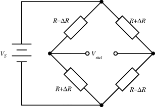
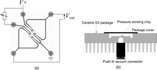
The first of these is a pressure sensor consisting of a micromachined cavity sealed with a flexible membrane. This could be fabricated from a variety of different materials depending on the mechanical properties required. Pressure differences between the sealed cavity and the surrounding atmosphere will lead to flexing of the membrane, which can be detected using polysilicon strain gauges in a Wheatstone bridge arrangement. The layout of the device is shown in Figure 8.9 alongside an image of the fabricated structure.
Figure 8.9 (a) Schematic layout of part of a MEMS pressure sensor with piezoresistive sensing. (b) Photomicrograph of a similar MEMS sensor.
The polysilicon piezoresistive strain gauges are short vertical tracks arranged in serpentine meanders. In Figure 8.9a there are four resistors in each arm of the bridge while in Figure 8.9b there are 8 resistors in each arm. The gauges are laid out so that two sets of resistors straddle the edge of the membrane (the central square in Figure 8.9a) while the other two are parallel to the edge and should not see significant stress. This is a type of ‘half-bridge’ sensor interface where only two resistors change with applied stress while the other two should be unaffected. Therefore, if the change in resistance in the gauges that are under stress is  and
and 
 R then the output voltage from the bridge will be:
(8.15) 
The Wheatstone bridge wiring includes a break in one arm which allows the addition of a variable resistor, as shown in Figure 8.10a, to balance the bridge at some set pressure. It could then be connected up to a differential amplifier or instrumentation amplifier to boost the output signal. Figure 8.10b shows how the chip was packaged by bonding it into a standard integrated circuit package which has had a hole bored through it with a high speed drill. The pressure can then be adjusted by applying a vacuum to the back of the device via a standard push fit connector. Micro-miniaturised pressure sensors such as this have many possible medical applications, particularly if they can be used monitor fluid pressures such as blood. This type of sensor can be integrated with other MEMS sensors and with CMOS electronics to provide amplification of the sensor outputs [4].
Figure 8.10 (a) Use of a variable resistor in a pressure sensor Wheatstone bridge to balance the circuit. (b) Schematic cross-section through a packaged pressure sensor.
The second example of piezoresistive sensing is a 3-axis MEMS accelerometer intended for use as a motion sensor capable of monitoring the activity of a beating heart. The specific application is described in more detail in [5, 6] but essentially the device would be stitched to the outer wall of the heart during bypass surgery to monitor for post-operative complications. The requirement was for a device that would be small enough to be removed when it was no longer needed, without the requirement for further invasive surgery, by pulling it out along the track of the wires used to connect it to the outside of the patients body. The complete packaged device is shown in Figure 8.11a and measures 5 mm by 3 mm by 1.5 mm. This includes hermetically sealed, biocompatible packaging which protects the moving parts of the sensor structure.
Figure 8.11 (a) Packaged MEMS accelerometer placed on a five penny coin (approximately 18 mm diameter) to show scale (courtesy of C. Lowrie and M. Desmulliez, Heriot-Watt University). (b) Microscope image of a MEMS accelerometer (reproduced from [5] with permission of the authors).
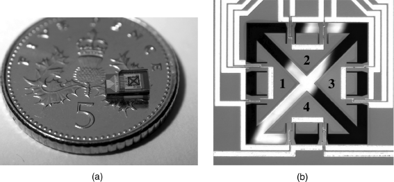
The MEMS accelerometer used in this case consists of four moving proof masses fabricated in a silicon on insulator (SOI) substrate. An SOI wafer consists of a standard thick silicon substrate, several hundred micrometers thick, topped with a thin buried oxide (BOX) layer and a thin device layer of high quality single crystal silicon. In advanced CMOS electronic processes this Si layer is used to fabricate devices with increased resistance to lock-up and radiation hardness but the BOX layer can also be used as an etch stop for bulk micro-machining. In this accelerometer device the moving masses are etched out from the bulk substrate from the back of the wafer and are suspended from thin cantilevers fabricated in the device layer of silicon. The movement of each of the proof masses is monitored using strain gauges fabricated as implanted resistors in the silicon cantilevers. There are 2 cantilevers for each mass and two resistors on each cantilever. This means there are 16 piezoresistors in total, arranged as four separate Wheatstone bridges. Figure 8.11b shows a typical accelerometer with triangular proof masses. The white metal tracks are interconnect for the piezoresistors which are not visible in this image.
In plane acceleration of the MEMS sensor will cause differential movement of opposite masses. So, in the case when there is movement in the X direction from right to left, mass 1 will move up while mass 3 moves down (refer to Figure 8.11b). Motion in the opposite direction would obviously cause the opposite effect while acceleration in Y would involve movement of masses 2 and 4. Out of plane accelerations in the Z direction would cause simultaneous motion of all four of the proof masses in the same direction.
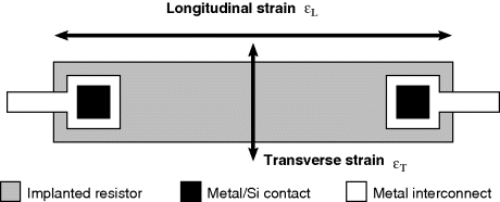
Sensing of this motion using implanted resistors in the single crystal silicon device layer is significantly more complicated than in the polysilicon resistors used in the pressure sensor. As was previously mentioned the effect of applied strain on the piezoresistive coefficient is the dominant effect in strain gauges fabricated in semiconducting materials. With careful choice of doping levels and crystal plane orientation, it is possible to fabricate piezoresistive sensors in silicon where the resistance increases when strain is applied in the longitudinal direction but decreases by a similar amount when the same strain is applied in the transverse direction. Figure 8.12 illustrates a possible layout for a simple implanted piezoresistor and indicates the different directions of applied strain. If the piezoresistive coefficients in the longitudinal ( ) and transverse (
 ) are such that
  then for a given applied tensile strain the resistance of a sensor orientated longitudinally will be:
(8.16) 
Figure 8.12 Schematic plan view of a diffused or implanted piezoresistor fabricated in single crystal silicon indicating the directions of longitudinal and transverse strain, defined relative to the direction of current flow in the resistor.
While the resistance of a sensor orientated transversely to the applied tensile strain is:
(8.17) 
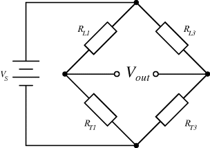
Each of the proof masses in the heart monitor device has two resistors in each cantilever arm and these are connected up into four Wheatstone bridges so that there are two bridges for the pair of X masses (1, 3) and two for the Y masses (2, 4). The piezoresistive sensors are arranged so that they are either orientated in the same direction as the strain induced in the cantilever when a mass moves (longitudinal) or at right angles (transverse). Finally, one of the bridge circuits for each pair of masses is designed to be sensitive to in-plane motion and insensitive to out-plane acceleration and vice versa. Taking the example of the sensor circuit for in-plane motion along the X axis, a longitudinal resistor ( ) will increase in resistance when in tension and decrease in compression while a transverse resistor (
 ) has the opposite characteristic. Figure 8.13 shows the arrangement of longitudinal and transverse resistors in the in-plane Wheatstone bridge. For in-plane acceleration from left to right the cantilever arms of mass 1 will bend upwards, compressing the piezoresistors, while the arms of mass 3 will bend downwards so the sensing resistors will be under tension. The result of this, assuming that the changes in resistance are all equal to
  and the nominal value is
  the values of the resistors in the bridge will be:
(8.18) 
(8.19) 
(8.20) 
(8.21) 
Figure 8.13 Arrangement of strain gauges in the X axis, in-plane Wheatstone bridge circuit from a MEMS accelerometer.
resulting in an output voltage:
(8.22) 
Similarly if the acceleration is out of plane, that is the device is moving into or out of the page looking at Figure 8.11b, both of the cantilever arms will be deflected downwards so that all of the resistors are under tension. Then the resistances in the in-plane sensing Wheatstone bridge will be:
(8.23) 
(8.24) 
(8.25) 
(8.26) 
These resistance changes will balance out and so the resulting output voltage due to this out-of-plane acceleration will be:
(8.27) 
Therefore this circuit is insensitive to out-of-plane acceleration but sensitive to in-plane accelerations along the X axis. By simply rearranging the connections of the Wheatstone bridge it would be possible to create a similar circuit which was sensitive to out-of-plane accelerations but not to in-plane movement.
8.3.3 Piezoelectric Effect
While piezoresistors are passive sensors requiring external power the piezoelectric effect can be used to make active sensors, and actuators. The phenomenon of piezoelectricity is the ability of some materials to generate an electrical potential when mechanically stressed. This is a two way effect and electrical inputs can cause a piezoelectric material to change shape. One of the most common examples in medicine is ultrasound where piezoelectric transducers both produce the ultrasound and sense the returning echoes.
Piezoelectric materials are typically crystalline, and contain fixed dipole charges which have some form of polarisation, that is the dipole charges are lined up in the same directions. Applying mechanical forces can move these charges around generating the measured potentials. The important point is that useful signals are only produced by changing the applied force, ‘dc’ mechanical signals do not produce any useful output. Piezoelectric materials range from natural substances like quartz crystal and bone, to synthetic compounds like lead zirconate titanate (PZT) and lithium niobate. Aluminium nitride is another interesting piezoelectric material as it should be possible to deposit thin films using microfabrication techniques for CMOS compatible mechanical actuation.
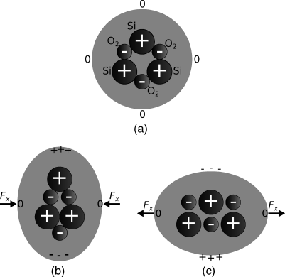
Figure 8.14 illustrates the effect of applying stress to crystalline quartz, which results in a redistribution of charge in the material.
Figure 8.14 (a) Arrangement of positive (Si) and negative (O2) charges in crystalline quartz. (b) Applying compressive stress redistributes the charge leading to a potential difference across the crystal. (c) Applying tensile stress has the opposite effect.
8.3.4 Quartz Crystal Microbalance
Quartz was the first piezoelectric material to be widely used, originally in the form of natural quartz crystals that were carefully cut to give the desired characteristics. The first, and still probably the most widely used piezoelectric sensor, was the quartz crystal microbalance (QCM), which consists of a very thin slice of quartz with thin film electrodes on either side, an example is shown in Figure 8.15. These are driven with an ac electrical signal which sets up a resonant standing wave in the piezoelectric crystal.
Figure 8.15 Quartz crystal microbalance, diameter 1.25 mm and thickness around 100 μm. Designed for use as a thickness monitor in a metal deposition system.
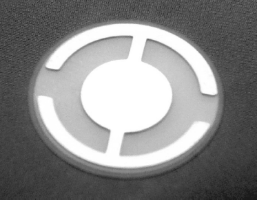
Figure 8.16 illustrates a common method of characterising resonant devices like the QCM by measuring the conductance or admittance while sweeping the frequency of the applied ac voltage. The conductance will show a characteristic peak at the resonant frequency  with a bandwidth
  . The quality factor
  gives a measure of the dissipation of the resonant energy and is defined as:
(8.28) 
Figure 8.16 Indicative plot showing a typical response of a QCM. Loading causes a change in the resonant frequency  and may also change the bandwidth
  (Adapted from http://en.wikipedia.org/wiki/File:QCM_principle.gif.
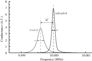
The resonant frequency is sensitive to the mass of the QCM and a common application of this sensor is as a thickness monitor in a thin film deposition process. If the material deposited is very thin or has similar mechanical properties to the QCM then the frequency will change in proportion to the deposited mass. If the material deposited is soft or viscoelastic then the  factor will change as well as the energy dissipation is increased. Measurement of biological materials in a liquid environment will generally increase the energy dissipation. CQM-D is a patented technique from a company called Q-Sense,1 which measures both the resonant frequency and the dissipation factor
  . This makes the QCM sensitive to the mechanical properties of the deposited film as well as just the mass and is targeted at biological sensing. Dissipation sensing is important when investigating chemical attachments in a liquid environment where there is significant damping. The sensitivity of the QCM is such that it can measure molecular binding events, for example in an immunosensing application using antibody/antigen binding or detection of specific DNA attachment.
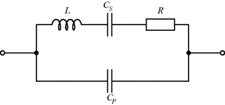
The equivalent circuit of a QCM at a frequency close to resonance is shown in Figure 8.17. The lower of the two parallel arms of the circuit has a capacitance  representing the physical capacitance of the parallel plate structure formed by the QCM, plus any parasitic effects from the connections. The upper arm represents the resonant properties of the piezoelectric crystal. The inductance
  and capacitance
  cancel out at the resonant frequency to leave the resistor
  which represents the dissipative energy losses. If the resistance is low that is equivalent to a high quality factor. Loading the QCM by attaching something to the surface can potentially change any and all of the resonant circuit elements.
Figure 8.17 Equivalent circuit for a quartz crystal microbalance.
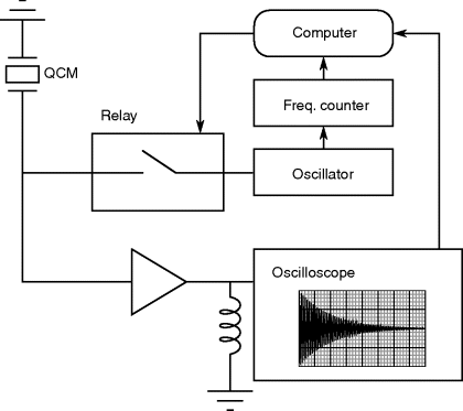
The initial paper on the QCM-D technique describes the instrumentation used to measure dissipation in a quartz crystal microbalance driven at its natural resonant frequency [7]. Prior to this the dissipation was often measured by monitoring the amplitude of the oscillation signal in the QCM, which is inversely proportional to  . However, this places limitations on how the microbalance is driven, for example there can be no automatic gain control which would tend to correct for dissipation. The solution detailed by Rodahl et al. used a setup similar to that shown in Figure 8.18. Here the QCM is driven into resonance and once it is oscillating stably a computer controlled relay disconnects the input signal. Simultaneously, an oscilloscope is triggered to capture the output signal from the QCM as the oscillations decay. The rate of decay of the signal provides a measure of the dissipation factor of the microbalance setup. The inductor after the buffer in the sensing part of the circuit will act as a high pass filter, removing any dc offset introduced when the relay disconnects the drive oscillator.
Figure 8.18 Instrumentation for dissipation measurements from a quartz crystal microbalance sensor, based on [7].
8.3.5 Surface Acoustic Wave Devices
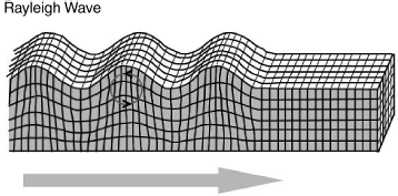
The quartz crystal microbalance is a bulk acoustic wave device meaning that the vibrations occur throughout the material. There is another class of piezoelectric resonant device that makes use of acoustic waves confined to the surface of a piezoelectric material. The Surface Acoustic Wave (SAW) shown in Figure 8.19 is known as a Rayleigh wave. This is the type of vibration that causes damage far from the epicentre of an earthquake but can also work with much smaller, faster vibrations in thin film materials. The movement here is purely at the surface, the vibrations only reach about one wavelength into the material and the amplitude of Rayleigh waves is normal to the surface.
Figure 8.19 Illustration of the propagation of a Rayleigh surface acoustic wave (Reproduced from http://earthquake.usgs.gov/learn/glossary/.).
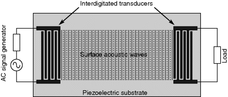
Surface acoustic waves can be excited in a piezoelectric substrate using an interdigitated transducer electrode (IDT) fabricated in a thin metal film on the surface of the substrate. The device shown in Figure 8.20 is known as a SAW delay line where the waves are transmitted along the surface between a transmission IDT connected to an ac signal generator, and a receiver IDT connected to a load. Another type might be a single transducer sending waves towards metal structures on the surface that reflect the SAW energy back to the input. They are often used to create high quality-factor filters and other RF components for use in mobile phones and other devices where the small size and high Q is important. Mobile devices with wireless connectivity rely heavily on SAW components.
Figure 8.20 Schematic plan view of a SAW delay line.
The resonant frequency ( ) of the SAW device will depend on the acoustic wave velocity (
 ) of the piezoelectric material and the pitch (
 ) of the IDT with the relationship in Equation (8.29), and typical SAW characteristic frequencies are in the range of 30–500 MHz.)

The SAW delay line can be turned into a sensor by making the substrate, and its acoustic properties, sensitive to parameter being sensed. The primary interaction mechanisms are those that affect the frequency or the delay between the transducers by changing the wave velocity, the IDT distance, or both. Temperature, strain, pressure, force, and the properties of a sensing layer added to the device are examples of quantities that can be measured. In particular, the accumulated surface mass produces a decrease in frequency so a SAW device can be used as a deposition monitor in a similar way to the QCM.
Biosensors can require a different type of SAW as Rayleigh waves will be dissipated through viscoelastic coupling with a liquid medium. Shear-Horizontal SAW waves require the crystal planes of the piezoelectric material to be orientated such that the induced waves are parallel rather than normal to the surface. Another alternative is the ‘Love wave’ mode of SAW, where a top coating of a material with low acoustic wave velocity is applied to the surface. This acts as a wave guide and prevents attenuation into the substrate or the surrounding liquid.
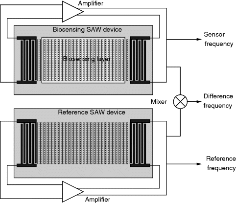
Most SAW biosensors operate by detecting mass loading as molecules attach to the prepared surface. By running two transducers in parallel, where only one has the chemically/biologically selective surface, you can compensate for cross-correlations with temperature or strain. As the devices have a characteristic resonant frequency, they can be driven into oscillation by an amplifier connected between input and output. The sensor output is the difference in frequency between the reference and sensor device. The reference device may have an additional blocking layer on top to prevent non-specific attachment. This experimental system is illustrated in Figure 8.21.
Figure 8.21 Possible arrangement for a SAW biosensing system which uses a pair of SAW delay lines, where one has a specific biochemical receptor layer while the other device acts as a reference to reduce effects of confounding factors.
SAW devices are also widely used in passive radio frequency identification (RFID) tags. With an antenna attached to the IDT they can pick up pulses of electromagnetic radiation from an RF transmitter. This excites a pulse of SAW energy that is reflected back by reflecting elements spaced like a barcode. The antenna retransmits the reflected pulses and by measuring the timing the ‘barcode ID’ can be calculated. A wireless SAW sensing device could have a single reflector and the delay of the pulse would carry information about the state of the sensor. A differential measurement could be made possible by using a double ended SAW sensor with the IDT in the centre. Only one SAW transmission area would be sensitive to the measured parameter so there would be also be a reference pulse to make the timing changes easier to interpret.
8.3.6 Capacitive Sensors
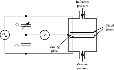
An alternative to piezoelectric or strain gauge transduction in mechanical sensors is the use of capacitance. This often involves something like a parallel plate capacitor where the movement is sensed as a change in the effective thickness of the gap between the plates. They have advantages of high sensitivity, if the gap is on the microscale, and low power operation compared to resistive sensing. The example shown in Figure 8.22 is of a pressure sensor that measures the difference in pressure between a reference chamber and a measurement chamber. Any difference will change the position of a moving membrane that forms one plate of a pair of complementary capacitors. This means that as one capacitance increases, as the membrane moves closer, the other will reduce. The capacitors are arranged in a bridge driven by an ac signal and the output voltage will depend on the ratio of the sensor capacitors.
Figure 8.22 Schematic representation of a pressure sensor using a capacitive bridge circuit for transduction.
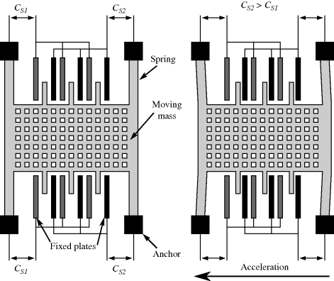
Capacitive sensing is the basis of some of the most successful MEMS devices, such as the surface micromachined accelerometers originally developed by Analogue Devices. These typically consist of a moving mass connected to the substrate through flexible springs, as shown on the left hand side of Figure 8.23. Along the edges of this proof mass are electrode fingers between pairs of fixed plates which form capacitors ( ,
,  ) to be used in sensing the displacement of the mass. When an acceleration is applied, as in the right-hand side of Figure 8.23, the mass will move in the opposite direction. This differentially changes the two capacitances and the movement can therefore be sensed by measuring the difference.
Figure 8.23 Operation of a surface micromachined MEMS accelerometer with capacitive sensing.
8.3.7 Capacitance Measurement
The values of the complementary capacitors ( ,
,  ) in a differential capacitive sensor can be represented in terms of the area
  , nominal separation
  , and the change in the position of the central plate
  . We can also define the nominal capacitance
  , when there is no movement.
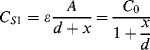
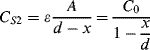
(8.32) 
These equations will only apply when the displacement  is relatively small compared to
  , as large deflections cause non-linearities. The increase in capacitance will lead to an increase in the electrostatic attraction between the plates, which is balanced by the mechanical spring force that tries to centre the moving mass. The mechanical design issues are beyond the scope of this discussion but a detailed introduction can be found in [8].
The small signal current in a capacitor can be represented by the following equation:
(8.33) 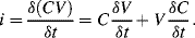
This equation has two parts to it, the first representing the familiar method of measuring a relatively constant capacitance with an ac voltage, where the current depends on the derivative of voltage with time. The second is possibly less familiar and suggests that you can measure a changing capacitance by applying a dc voltage. In terms of capacitance based sensors, the first term represents the measurement of a relatively slow variation of capacitance using a high-frequency ac voltage. This is the case in an accelerometer or pressure sensor where fc fv. The second case would be a capacitance that changes very quickly, for example in a MEMS microphone with capacitive feedback, where a dc voltage can be applied and will produce a current signal dependent on the rate of change of capacitance. This discussion will focus on the measurement of slowly varying capacitances through the application of ac drive voltages.
The displacement in a differential capacitive sensor can be sensed by measuring the current output of the circuit shown in Figure 8.24. An ac voltage with a frequency  (
( ) and amplitude
  to the top of the pair of capacitors and the inverse of the voltage signal (
 ) to the bottom. The central point ‘A’ is effectively grounded through the low impedance ammeter. The current through the upper capacitor
  into the measured node will be:
Figure 8.24 Measurement circuit for differential capacitive sensors.

while the current through  into the measured node is:
If Equations (8.34) and (8.35) are added together and the expressions for the capacitances in terms of the displacement (8.30) and (8.31) are substituted in then the result is:
(8.36) 
This is a function of the displacement but there are second-order terms as well that can be an issue if it is not the case that x « d. If this is the case then the term for  can be ignored and the equation simplifies to:
(8.37) 
This current could be measured with the current follower or transimpedance amplifier examined in Chapter 7, Section 7.4.6 but there are other methods of transduction for capacitive sensors that may be more appropriate depending on the application.
8.3.8 Capacitive Bridge
An alternative to current measurement is to use a capacitive bridge circuit (see Figure 8.25a) as in the sensor in Figure 8.22. In a half bridge arrangement two of the capacitances will vary with the displacement of the sensor in a push-pull arrangement:

(8.39) 
Figure 8.25 (a) A bridge circuit for capacitive sensors without parasitic capacitances. (b) Similar circuit with parasitics on output terminals.
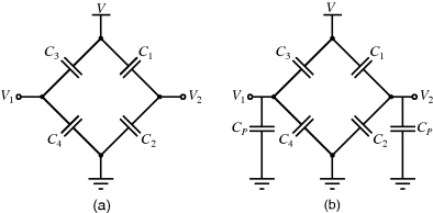
While  and
and  will both be equal to the nominal capacitance
  . Then the output voltages (
 ,
,  ) will be:
(8.40) 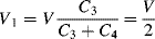
(8.41) 
The overall output voltage of the bridge is then:
As with the resistive bridge circuits the use of a full bridge arrangement, where all four of the capacitances vary with displacement, will double the sensitivity of the system if the two sides of the bridge are working in opposition.
Parasitic capacitances can be a problem with this type of measurement as these can be significantly larger than the actual capacitances being sensed. A parasitic ( ) to ground on both of the bridge outputs (see Figure 8.25b) will have the effect of lowering the effective sensitivity of the capacitive sensor. Using the same half bridge arrangement as before but defining the differential sensing capacitors as:
(8.43) 
(8.44) 
The output voltage without the parasitic capacitances (Figure 8.25a) will be:
(8.45) 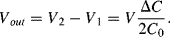
While the output voltage with the parasitics will be:
(8.46) 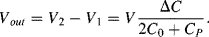
There are a number of different possible sources of parasitic impedances, including the electrical connections made to the sensor, capacitances in the active components of the instrumentation and parasitic capacitances in the actual MEMS structure, for example between the suspended moving elements and a conductive substrate. If the conductive plane which has parasitic capacitances to a measured capacitor is not grounded then effectively you have the series combination of the parasitics in parallel with the sensing capacitor. Changes in the parasitics will directly affect the measurement which is obviously undesirable.
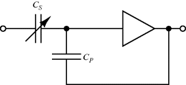
Bootstrapping is a common method of dealing with parasitics which attempts to eliminate any current flow in them. With a parasitic capacitance on a signal line this can be achieved by driving the other side of the capacitor with the same signal through a buffer amplifier (Figure 8.26). This technique is applied in triaxial cables, commonly used for low level signals, where the inner conducting core is surrounded by a guard conductor that is driven with the same signal as the core. This is subsequently surrounded by a grounded shield conductor as in a coaxial cable.
Figure 8.26 Bootstrap method for eliminating the effect of parasitic capacitance  on the measurement of sensor capacitance
  .
.
The current measurement method mentioned previously is another useful way to reduce the effects of parasitic capacitance between a signal line and ground. A low impedance current meter or a virtual ground, like the input of a operational amplifier configured as a current follower, will have the same effect as bootstrapping by removing the voltage drop across the parasitic.
There are a number of non-ideal effects in the fabrication or the subsequent operation of capacitive MEMS sensors, and some of these may be reduced or compensated for by using force feedback control. Here, the output from the sensor interface is fed back, through a large resistance, to the central output terminal of the sensor. This negative feedback applies a balancing electrostatic force which serves to keep the moving mass centred and the displacement as small as possible. The output should then be a linear function dependent on the electrostatic force applied to stop the mass from moving under acceleration.
8.3.9 Switched Capacitor Circuits
There are a number of different reasons to favour capacitors over resistors for biasing in amplifier design, particularly in integrated circuits. Where high-value resistors are required, for example in current to voltage converters for low current measurement, the integrated components may be prohibitively large and there are other problems such as thermal noise, component matching and temperature dependence. Capacitor ratios may be set relatively easily in integrated circuit processes, though the absolute values will vary, and they are less prone to temperature dependence or thermal noise. Capacitors generally have a smaller footprint area than equivalent resistors and do not represent a dc load, which may be important for CMOS based op-amps where the output impedance can be significant.
Simply replacing resistors in an op-amp circuit with an equivalent ratio of capacitors could work for some signals but they will be open circuit for low frequency voltages meaning there is no dc feedback to the inverting input. This is not compatible with stable op-amp circuit design and so the alternative is to use a switched capacitor amplifier such as that shown in Figure 8.27. This is a simplified circuit that does not take into account parasitics or other non-ideal behaviours but it is useful for illustration of the approach. There are three switches, which are driven by two non-overlapping and complementary clock signals as shown in Figure 8.28. This is a non-inverting amplifier, although it resembles the layout of the inverting amplifier, and has a gain set by the capacitor ratio  . The best way to understand it is to look at the circuit during each of the clock cycles. In cycle
  , where
  and
and  are closed and
  is open, capacitor
  is connected to
  at one end and the inverting op-amp input, that is a virtual earth, at the other end. If the previous stage can supply sufficient current then by the end of cycle one the capacitor will be fully charged to
  and the charge will be:
  . The other capacitor (
 ) is discharged and the amplifier output
  V.
V.
Figure 8.28 Non-overlapping clock signals to control a switched capacitor amplifier.
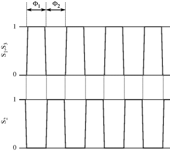
Figure 8.27 Switched capacitor amplifier with non-inverting function.
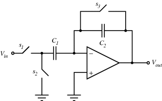
At the start of cycle  ,
,  and
and  will open while
  closes. Now the op-amp would like both ends of
  to be at the at the same potential (ground) and so it will be discharged. The current required to do this will flow through
  and so the charge is transferred between the two capacitors such that:
  . At the end of this charge transfer, which should be complete by the end of cycle
  , the voltage on the output will be:
(8.47) 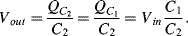
Therefore, this is a non-inverting amplifier with the gain set by the capacitor ratio. Another way to think about this circuit is as an amplifier with sample and hold functionality where the input signal is sampled at the time point where we change from cycle  to cycle
  .
.
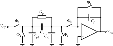
The circuit in Figure 8.29, is similar to the previous switched capacitor amplifier but is more proof against parasitic capacitances. It can be used as a capacitance to voltage converter to measure the unknown capacitance  . As before there are two, non-overlapping, switching cycles
  and
and  . The parasitic capacitors
  ,
,  and the parasitic leakage conductance
  are not dealt with in detail here and a more complete description can be found in [9]. In short, the parasitic capacitances are shorted out by the parallel switches in order to reduce their effects on the charge transfer. In any case, when the
  switches are closed
  is charged to
  , while the feedback capacitor
  is discharged. Then in cycle
  ,
,  is discharged and the accumulated charge is transferred onto
  . Again, the output voltage at the end of this cycle will depend on the ratio of the two capacitors:
(8.48) 
Figure 8.29 A switched capacitor circuit capacitor circuit with an output that depends on the value of the unknown capacitance  .
.
The previous circuit allowed the measurement of a single unknown capacitance but Figure 8.30 shows an alternative scheme for the measurement of a differential capacitive sensor using a switched capacitor integrating amplifier. The operation of this is as follows. The sensing capacitors are driven with square waves that are not only 180° out of phase but also dc shifted so that  goes from, for example, 0 to 5 V and
  goes from 0 to −5 V. Therefore the capacitors will be charged in different directions and the overall charging current will be dependent on the difference between them. The excess charging current, if
  , has to flow through
  , assuming no current flow into the op-amp inputs. Therefore,
  will integrate this charging current in each cycle and the output voltage will depend on the difference
 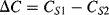 and the value of
  :
:
(8.49) 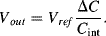
Figure 8.30 Switched capacitor integrating amplifier which could be used to measure a differential capacitive sensor.
The reset switch will discharge  once each cycle so that the starting value of
  is always zero. The reset switch is driven with a signal that has half the frequency of the inputs so that it captures one whole cycle of charge from each capacitor. The output is low pass filtered to remove the modulation introduced by the
  and
and  signals. Dealing with all of the parasitics in a capacitive sensor would require a much more complicated switched capacitor amplifier than can be sensibly covered by the current work. An example of such a circuit can be found in [10].
8.4 Optical Biosensor Technology
8.4.1 Fluorescence
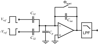
This section will examine a number of different sensor technologies but generally focusses on optical sensors using fluorescence as this is by far the most widely used technique in biosensing. Figure 8.31 shows a Jablonski energy diagram illustrating the phenomenon of fluorescence. Briefly, a fluorescent material absorbs a photon which excites an electron from a ground state to a higher energy level. When it decays back down to the ground state, after some delay, it can re-emit a photon at a lower energy. Figure 8.31 is a relatively simplified version of the Jablonski diagram, which does not show all the different ways in which an excited electron can lose energy, many of which do not lead to emission of a photon by fluorescence. The main point to take away is that the emitted photon will have a lower energy than the absorbed photon. The energy of a photon is expressed by this formula:
Figure 8.31 Energy band diagram illustrating the phenomenon of fluorescence.
(8.50) 
where  is Planck's constant and
  is the frequency of the light. If the emitted photon has a lower energy then it will necessarily have a different wavelength
  as:
as:
(8.51) 
where  is the speed of light. This change in the wavelength of the emitted fluorescent photons compared to the absorbed excitation light is referred to as the Stokes shift after George Stokes who first described fluorescence. In addition to the change in wavelength there will also be a time delay between the excitation and emission. The average time between the absorption of a photon and the subsequent emission is the fluorescence lifetime. This can be quite different for dyes with very similar emission wavelengths and can be used as the basis of biosensing techniques. The final value that characterises a fluorescent material is the quantum yield or efficiency, which is the ratio of photons emitted versus the number of photons absorbed, and is always less than 1.
For many years fluorescence has been the most widely used tool for qualitative measurements in biology and biochemistry. There are two principal methods in which fluorescence is used in cell biology and biosensing. Firstly there are extrinsic fluorescent labels or fluorophores which have been deliberately introduced to the biological system. These can be attached to whatever is being investigated, for example an antibody, and once it attaches to a cell or antigen then the fluorescent emission can be used to detect this specific binding event. The alternative to this is intrinsic fluorescence, where certain cells or organisms either naturally produce fluorescent proteins like the now common Green Fluorescent Protein (GFP) or have been genetically modified to express it.
Fluorescence is not only used at a cell level, one of the most common and important uses of fluorescence in biosensing is in microarrays. Glass slides or chips may be prepared with arrays of microscopic spots of biosensing probe molecules, for example these could be specific lengths of single stranded DNA or antibodies. The target molecules then have to be labelled with specific fluorophores and will attach to their complementary probes on the surface. By measuring intensity of the fluorescence from each spot the presence of the target molecules in the sample under test may be determined. However, the fact that the targets need to be labelled is a limitation on the process and the reason why research into ‘label-free’ biosensing techniques is so important for the future.
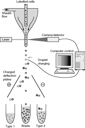
One of the most common fluorescence based analytical techniques in cell biology is Fluorescence Activated Cell Sorting (FACS). This is a type of flow cytometry; a high throughput measurement of cells which involves flowing them past a sensor then sorting them based on the result, as illustrated in Figure 8.32. The starting point for FACS is a heterogeneous population of cells that are labelled with one or more fluorophores based on the expression of some marker on the cell surface or within the cell. Next the cells are confined into a narrow sheath flow channel so that they are separated into a stream of single cells. At this stage they are illuminated with a laser and the resulting fluorescence is measured, often along with an estimation of the size of the cell. Next the suspended cells are dispensed from narrow nozzles designed to produce droplets with no more than one cell in each. Depending on the results of the fluorescence measurements these droplets have an electric charge applied to them which means that they can subsequently be deflected by charged plates into a number of different reservoirs. FACS is a very fast and accurate way to gain statistical information about a cell population but it does require that the cells are labelled, and the high flow rates used are likely to damage the cells through shear stress. This means that FACS is not suitable for some cell types such as stem cells to be used in clinical applications. In many cases it can be considered to be a destructive technique and there is considerable interest in other characterisation or sorting methods for cells which are label free and do not cause damage.
Figure 8.32 Schematic diagram illustrating the function of a fluorescence activated cell sorting system.
There are a number of different techniques for fluorescence microscopy but the following are some of the most commonly used methods:
- Spectroscopy: A basic method where the intensity of light emission is measured over a range of different wavelengths to get information about the different fluorescent materials in the sample.
- FLIM (fluorescence lifetime imaging microscopy): This technique looks at the lifetime of the fluorescence rather than the intensity and has some advantages which will be covered later in the chapter
- TIRF (total internal reflection fluorescence): This makes use of evanescent field effects for very sensitive measurements. TIRF effects are important in fibre optic based sensors covered later in the chapter.
- FRET (Förster resonance energy transfer): This exploits pairs of fluorescent dyes and can be used for sensitive molecular measurements. A case study later in the chapter will explore this more fully.
There are a number of ways in which the fluorescence of a fluorophore can be affected by the environment or by the measurement itself. Photobleaching is a consequence of exposing the dye to the high energy excitation radiation which can gradually alter the chemical structure of the dye leading to a reduction of fluorescence. This can be exploited for certain measurements or reduced by making sure that excitation is kept to short pulses or with reduced power. Quantum dots are a special case as their fluorescence is a consequence of their physical structure and they are not generally subject to bleaching. Quenching is a reduction of the fluorescence caused by environmental parameters, usually chemical in nature. This can therefore form the basis of a chemical sensor.
8.4.2 Optical Fibre Sensors
Many of the techniques for optical analysis or measurement of biological and chemical materials, functions and reactions are suitable for adaption for use in sensors based on optical fibre technology (or other optical waveguides). In addition there are a variety of physical sensors which can also make sure of optical fibres. Optical fibres have low losses and so they can be used to locate a remote sensor a significant distance from the optical detection and light source. When compared to a wireless sensor the fibre sensor still needs a physical link but there are also advantages in certain environments due to the fact that there is no need for an electrical connection for power or signal transfer. For example, this can be a significant advantage for sensors in liquids where corrosion is a problem or where sparks could lead to risks of explosions. In addition, optical fibres have little or no problem with interference and have a high sensitivity and bandwidth.
Optode (occasionally referred to as optrode) sensors are physical or, more commonly, chemical transducers which are interrogated optically. These may or may not use optical fibres as part of the sensor system but many do, and there are two main forms that this can take. In an extrinsic sensor the fibre simply guides the light to and from the sensing element but in an intrinsic sensor the fibre itself becomes part of the transduction. This could happen through a mechanical interaction such as the bending of the fibre altering the light path or through some other type of interaction, possibly chemical in nature, which changes the propagation of light in the fibre.
In an extrinsic optical sensor, where the fibre acts as a guide for the light to and from the actual sensor, the are many different possible sensing modalities. The light could pass through the sensing element where the absorbance changes with the parameter being sensed or it could reflect off a surface. Membrane pressure sensors with the bandwidth to measure pressure waves from explosions are an example of a physical sensor using reflection, as is a gas sensor with a membrane that expands and bends as the analyte is absorbed into it. Some materials may change in reflectivity due to a chemical interaction with the environment or produce fluorescence.
One example of an optode using fluorescence is that of an oxygen sensor which exploits the quenching effect of oxygen on ruthenium based fluorophores. Sensing layers can be immobilised on the tip of an optical fibre in a structural matrix which is then coated with an oxygen permeable membrane such as Teflon. A good example of this is a fibre sensor which uses an oxygen sensitive coating on the tapered tip of a multimode fibre which can carry both the excitation and emission wavelengths. The tapered tip increases the interaction of the light with the fluorophore and this aids the sensitivity of the sensor [11].
The operating principle of an optical fibre makes use of the phenomenon of total internal reflection at the boundary between the core of the fibre and the surrounding cladding. Assuming the light hits the interface between the core and cladding at an angle shallower than the critical angle for the materials, then there will be total reflection and efficient transmission of the light down the fibre. However, there is also a so-called evanescent wave that extends beyond the boundary but decays exponentially. This has been described previously in Chapter 4, Section 4.3.5. The effective extent of the near field evanescent wave is typically less than the wavelength of the light but this is enough for it to interact with the material close to the interface and, for example, excite fluorescence in a sensing layer as in TIRF. This sensing layer could be could be biological in nature, such as an antibody probe which fluoresces when labelled targets are attached. The sensing region in an intrinsic fibre sensor can be distributed over the length of the fibre or confined to specific points. The penetration depth of the evanescent wave is very low so if the fibre becomes coated with a fouling layer, which will depend on the environment, it can stop it working properly. On the other hand, sensing using this evanescent illumination is considered to be very sensitive to changes in the very thin layer into which it penetrates.
8.4.3 Optical Detectors
There are many different methods by which the light from an optical biosensor can be transduced into a meaningful electronic signal. One of the simplest photonic transducers is the photoresistor or light-dependent resistor. This is a conductometric sensor based on a semiconducting material. Exposing this to light leads to the generation of mobile charge carriers in the semiconductor which decreases the resistivity of the material. Photoresistors are relatively crude but can provide useful information about the overall intensity of light, for example as an exposure metre for a camera. The wavelength of light to which the photoresistor is most sensitive may be controlled by doping the semiconductor, which will change the energy required to raise an electron to the conduction band.
The photomultiplier tube (PMT) illustrated in Figure 8.33, is an extremely sensitive single photon detector and still the best choice for many low level measurements, regardless of the fact that it relies on pre-solid-state, vacuum tube technology. The PMT consists of a sealed glass tube under high vacuum with a number of delicate metal electrodes inside. At one end is a photocathode that uses the photoelectric effect to produce an electron when struck by a photon. This is accelerated towards a dynode electrode held at a more positive voltage. This acceleration gives the electron additional energy so that when it hits the dynode it can excite more than one electron to be emitted. These are then accelerated towards a sequence of additional dynodes, each of which is held at a higher positive voltage than the last. Finally, at the end of the tube is an anode which receives a pulse of current due to the multiplication of the electrons which happens at each of the dynodes. This amplification effect means that the PMT is extremely sensitive as each photon can potentially produce an output current made up of a large number of electrons. Therefore it has a quantum efficiency, meaning the number of electrons out per photon input, which is greater than unity. A common use for the PMT in biomedical imaging is in a positron emission tomography (PET) system. Positron annihilation produces gamma radiation which can be converted to visible light with a scintillator. The PET scanner uses a ring of PMT detectors with scintillators in front of the photocathode.
Figure 8.33 A schematic representation of a photomultiplier tube which can act as a sensitive optical detector.
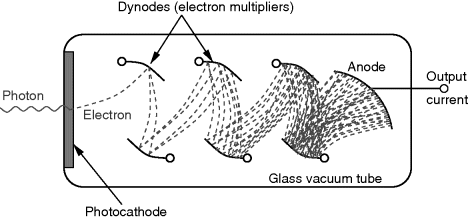
There are a number of solid state devices that can be used as optical detectors and have advantages of small size and high speed of operation. The photodiode illustrated in Figure 8.34 is a p-i-n structure though p-n diodes can also be used as optical sensors. Photodiodes are operated in reverse bias, meaning that there is only a small leakage current and a wide depletion region. When they are exposed to light, photons of sufficient energy can be absorbed to generate electron hole pairs. If this happens in the depletion region the carriers are swept apart by the electric field before they can recombine and a photo-generated current will flow. The advantage of a p-i-n structure over a p-n diode is the wider effective depletion region meaning a higher quantum efficiency and a lower capacitance which can increase the bandwidth.
Figure 8.34 Cross sectional schematic illustration of a p-i-n photodiode structure.
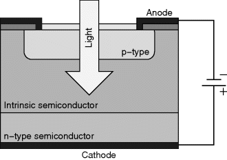
In a standard photodiode the quantum efficiency is always less than unity because each photon can only excite at most one electron-hole pair. However, it is possible to design photodiode structures which can provide amplification of the carriers generated by photon absorption. The single photon avalanche photodiode (SPAD) is designed to be biased well into breakdown, where normally a high current would be expected. In a SPAD though this does not occur until a carrier pair is generated in the depletion region at which point a spike of current will occur through an avalanche breakdown process which is similar to the electron multiplication in a PMT. SPADs are biased with a resistance in series, as shown in Figure 8.35, which can either be an actual resistor or an appropriately biased transistor. When the SPAD goes into breakdown the current flows through this resistance which reduces the voltage across the device and quickly brings it out of the avalanche breakdown region of operation. This is known as passive quenching and a SPAD biased in this way operates in a ‘Geiger-mode’ where each photon will generate a spike of a few picoseconds duration on the output. These spikes can be counted to provide a number related to the intensity of the light which has a very high dynamic range. This range will be between the ‘dark-count’, a noise floor dependent on the spontaneous generation of carriers in the device, and some maximum level where photons are arriving too close together to be able to detect each one. The fact that the device can accurately measure the time of arrival of each photon means that SPADs can potentially be used for three-dimensional imaging through ‘time of flight’ measurement [12] or as part of a fluorescence lifetime imaging microsystem [13].
Figure 8.35 Simplified passive quenching circuit for a single photon avalanche diode (SPAD) operated in a Geiger mode.
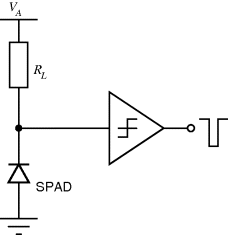
The charge coupled device (CCD) was originally developed in the 1960s as a memory device and consists of an array of gate electrodes separated from a semiconducting substrate by a thin dielectric. Packets of charge can be stored in doped channels under the electrodes and moved between adjacent pixels in a row by changing the voltage on the gates. Although it was conceived as solid state memory it was soon found that charge could be generated through the photoelectric effect when the array is exposed to light. In a modern digital camera a two-dimensional CCD array is exposed through a lens, and a colour filter, to give a pattern of charge relating to the light exposure. This is then read out by moving the charge packets along a row and measuring the intensity of each pixel at the end. The CMOS camera is a more modern alternative to the CCD camera which is common in certain applications, such as mobile devices, due to the smaller size. High end camera sensors still tend to be CCD based as the integrated circuits on a CMOS camera usually mean that the proportion of each pixel taken up by the light sensitive area is lower. A CMOS camera chip is typically made up of an array of photodiodes integrated with electronics for row and column addressing. SPAD sensors may also be integrated with CMOS electronics to provide readout, addressing and even time resolved photon counting in each individual pixel.
8.4.4 Case Study: Label Free DNA Detection with an Optical Biosensor
This section will discuss a biosensor system which uses a combination of an artificial DNA structure that operates a switch, fluorescence based readout and a control mechanism using electrochemistry and microfabricated electrodes. Therefore, it combines many of the different techniques covered in this book.
Förster resonance energy transfer or FRET has been mentioned previously in Section 8.4.1 and its application in biosensing is described in Chapter 6, Section 6.9. It relies on the use of a pair of fluorophores where the emission spectrum of one dye (donor) overlaps with the excitation spectrum of the other (acceptor). Under suitable conditions, excitation of the donor fluorophore leads to energy transfer to the acceptor and emission of a different wavelength of light than would be expected from the donor alone. This is illustrated in Figure 8.36 which shows FRET between cyan fluorescent protein (CFP) and yellow fluorescent protein (YFP). The energy transfer effect only happens over short distances, the Förster length is typically a few nm, which is significantly less than the wavelength of the light used to excite the donor. The acceptor effectively quenches the donor, reducing the energy that would cause it to fluoresce.
Figure 8.36 (a) When fluorophores are separated by more that the Förster distance there is no energy transfer and fluorescence emission from the donor (CFP) is seen. (b) When the dye molecules are close together FRET occurs and emission from the acceptor fluorophore can be observed.
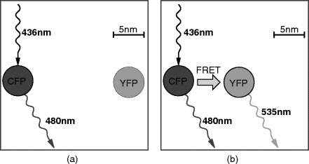
FRET can be exploited in a biosensor if it is possible to arrange for the dyes to be brought together to indicate the presence or absence of whatever is being measured. For example in an immuno-assay where the antibody probe is labelled with one fluorophore and the target is labelled with the other. The sensor discussed here avoids the need to label the target molecule through the use of a specific DNA structure known as a Holliday junction (HJ). This is a 4-way junction of DNA strands that is usually artificial but does occur naturally in certain biological processes. The biosensor exploits the fact that this molecule can be switched between two different conformations as illustrated in Figure 8.37. It is believed that the change in the HJ from the open to the closed conformation occurs when it is exposed to cations, which act to screen charges in the HJ that normally prevent the collapse of the structure.
Figure 8.37 Schematic representation of a Holliday junction which can switch between two different conformations.
The HJ can be turned into a sensor by attaching FRET fluorophores to the arms so that they are kept apart in the open conformation and brought together in the closed. This means that the FRET signal can be turned on and off by controlling the concentration of cations in the environment of the HJ molecule. Figure 8.38 shows the way in which the emission spectrum of the FRET will change depending on the HJ conformation. With no FRET (open conformation) the spectrum is dominated by the emission peak from the donor fluorophore but when the HJ is closed this peak is lowered due to quenching and a second peak can be observed indicating fluorescent emission from the acceptor. The conformation of the molecule can be measured with a ratiometric technique where the intensity of the fluorescence is measured at the peak emission wavelengths of the two dyes. The ratio between these intensities will provide information about the level of FRET and therefore the shape of the HJ.
Figure 8.38 Representative graph of emission spectra from a pair of fluorescent dyes on an HJ with (closed) and without (open) FRET occurring.
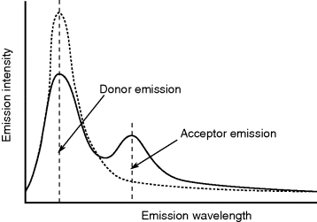
The HJ can be applied as a biosensor which is capable of detecting a specific sequence of nucleotides through the creation of an incomplete HJ molecule made up from only three strands of DNA. In this molecule, two arms of the probe junction will be incomplete and should have complementary sequences to the single stranded target DNA. Hybridisation of the probe and target will complete the Holliday junction structure. The incomplete probe-HJ will already have FRET fluorophores attached so the target DNA does not need to be labelled. The probe-HJ will not switch to allow FRET and so we can determine the presence of the target DNA sequence by actively switching the completed Holliday junctions and measuring the change in the fluorescence ratio. This type of biosensor has been demonstrated using changes in the concentration of Mg2+ ions to switch the completed HJ molecule [14]. In addition, it has been shown that a similar sensor using fluorescence lifetime measurements to detect the FRET effect is capable of detecting changes to a single nucleotide in the target molecule [15].
Those publications demonstrate the technique using changes in the bulk concentration of ions in the solution around the HJ molecules but it is also possible to use electrochemical methods to change the ion concentration. This opens up the possibility of a biosensor microsystem using this technique where the switching ion concentration is controlled with microfabricated interdigitated electrodes. These are fabricated in platinum before one half of the electrode pair is electroplated with silver and converted into a Ag/AgCl reference/counter electrode. The other half, the working electrode, is coated with an electrochemically active polymer film which is loaded with magnesium ions. Applying positive voltages to the ion switching film (WE) versus the RE causes the release of the Mg2+ ions while a negative voltage will lead to reabsorption of ions from the solution into the film.
In the prototype system used in initial experiments the incomplete HJ probes were spotted onto glass coverslips in a similar process to that used in making DNA microarrays. These are then fixed over the microelectrodes with an adhesive spacer in between. The chambers above the electrodes are filled with a solution, which acts as a buffer for the electrochemistry, before they are sealed. The buffer solution also contains either a complementary oligonucleotide to complete the HJ or a non-complementary target which will act as a control. Figure 8.39 shows an assembled device and full results can be found in [16].
Figure 8.39 Photograph of an assembled lab on a chip system for the study of Holliday junction based DNA sensors using on-chip electrochemical switching.
8.5 Transducer Technology for Neuroscience and Medicine
This section will cover an important area of research and development in biomedical engineering, where microsystems technology is applied to the problems of interfacing electronics with nerves or brain tissue. Chapter 3 has introduced the electrogenic behaviour of certain cells and tissues, the most important being the neuron. This section will continue with a review of the different methods that are available for measuring the activity of neurons and interfacing with them in the laboratory. However, it is important to first describe the structure of the neuron in more detail.
8.5.1 The Structure of a Neuron
Figure 8.40 shows the structure of a typical neuron, the basic cell of the nervous system. The main cell body is often referred to as the soma and contains the nucleus and the rest of the cellular machinery that keeps the cell alive and working. The neuron is electrically excitable, as described in Chapter 3, and has inputs and outputs. The inputs are the dendrites which receive signals from other neurons, while the output is via the axon. This is a long cellular process and each neuron can only have one, though it usually has multiple branches and terminals at the other end where it connects to the dendrites of other neurons. Axons can be extremely long, sometimes even extending the entire length of the organism they are part of. In order to speed the transmission of signals along the axon, most neurons in vertebrates have myelination of the axon process. The myelin sheath is an insulating layer formed by glial cells that reduces the capacitance of the cell membrane allowing the action potential to move more quickly. The regular gaps in the myelination are known as nodes of Ranvier and contain large concentrations of ion channels. The action potential effectively jumps from one node to the next as it is transmitted down the axon, in a process known as saltatory conduction. Diseases which cause the loss of myelination, such as multiple sclerosis, can have a serious debilitating effect on the nervous system by affecting the transmission of signals down axons.
Figure 8.40 Schematic diagram of the structure of a neuron.
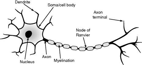
8.5.2 Measuring and Actuating Neurons
One of the first methods of electrically interacting with neurons to be developed was the voltage clamp, which involves inserting electrodes into the cell to control the potential across the membrane without interference from ion channel effects. This was first achieved with the squid giant axon, which is around 1mm in diameter, as it was large enough for the insertion of the macroscale electrodes available in the 1950s. The reason for the large size of the squid giant axon is that most invertebrates like molluscs do not have myelination of their axons meaning that a large diameter is required for fast transmission of action potentials over significant distances. This experiment allowed the researchers involved to monitor the opening and closing of ion channels during an action potential for the first time. As technology developed it became possible to fabricate microscale glass capillary electrodes to perform similar experiments in much smaller cells, such as mouse neurons. The voltage clamp technique is illustrated in Figure 8.41. It involves the insertion of two glass capillary electrodes through the cell membrane into an axon where they make contact with the cytoplasm. One of the internal electrodes, to the right of the figure, is connected to the high impedance input of a differential amplifier with a low gain. It is used to sense the membrane potential  between the internal electrode and an external potential sensing electrode. This potential is fed into one input of another differential amplifier along with a control voltage
  . The output of this high gain amplifier is connected to the other capillary electrode, which will force a current into the cell in order to try to make the measured membrane potential equal to the control voltage. The current required will balance the net flow of charge into or out of the cell through the ion channels in the cell membrane. Therefore this technique can be used to study voltage gating of these ion channels by modulating the membrane potential and recording the membrane current,
  . This current can be monitored with a pair of external sensing electrodes by measuring the voltage drop in the solution across a short distance. This voltage drop will be dependent on the resistance of the solution,
  so that:
(8.52) 
Figure 8.41 Schematic diagram of a voltage clamp setup for electrophysiology.
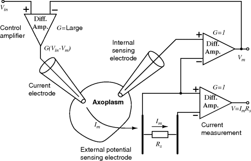
It should be clear from Chapter 7, Figure 7.15, that this technique, and the instrumentation used, is analogous to the potentiostat in electrochemistry.
An alternative method for the investigation of the electrophysiological behaviour of neurons and other electrogenic cells is the current clamp, which is illustrated in Figure 8.42. A single capillary electrode is inserted into the cell, and is used to inject a controlled current. This could be used to model the excitation of an ion channel for example. The injected current is generated by controlling the voltage across the resistor  , and this is achieved by sensing the probe voltage
  relative to the earthed culture solution with a voltage follower. This probe voltage is added to the control voltage
  with a summing amplifier, and this feedback will try to keep the voltage across
  equal to
  . The current flow into the cell will then be:
Figure 8.42 Schematic representation of a current clamp setup for electrophysiology.
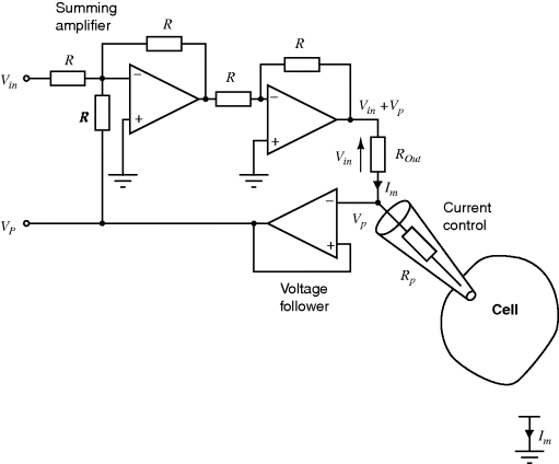
(8.53) 
which can either be monitored by placing a current follower circuit, similar to that used to sense working electrode current in a potentiostat, on the solution reference electrode or by adding a differential amplifier to measure the voltage across  . The probe voltage
  is not exactly the same as the membrane potential of the cell as there is an additional voltage drop due to the resistance of the capillary electrode, which can be considerable.
The patch clamp technique, as described in Chapter 3, Section 3.15, involves the use of a very fine-drawn glass needle, filled with an electrolyte solution and including a suitable measurement electrode. A highly accurate micropositioning system is used to bring the needle into contact with a neuron while the cell is viewed through a microscope. Suction is applied to the needle to create a tight seal to a patch of the cell membrane. This is often referred to as a ‘giga-ohm seal’ or ‘gigaseal’ because the resistance between the inside of the needle and the solution surrounding the cell should be very high. The patch clamp technique potentially allows the measurement of the current through a single ion channel as it is manipulated by changing the cellular environment. For example the needle may be preloaded with neurotransmitter chemicals to activate ligand-gated ion channels or the potential on the electrode may be manipulated to control voltage gated channels. If the pressure used to suck the cell onto the needle is increased beyond some critical point it can break the membrane and allow access to the cell interior for whole cell measurements. This is destructive to the cells as the electrolyte in the needle gradually replaces the cytoplasm, meaning that the measurements are only useful for a few minutes after the membrane is broken. Other patch clamp techniques may involve tearing a small piece of cell membrane away so that it can be studied separately, either with the original inside surface facing outwards or the other way around. As with the whole cell measurements, these ‘inside-out’ and ‘outside-out’ patch techniques are typically destructive to the cell.
An example of a possible instrumentation setup for patch clamp measurements, often referred to as a head-stage amplifier, is shown in Figure 8.43. Here the current is sensed as the voltage developed across the feedback resistor  in an op-amp current follower circuit. The non-inverting terminal of the op-amp is connected to an input voltage signal
  and, due to the feedback, this will control the potential on the pipette electrode. The input voltage and the output of the op-amp are then fed into a differential amplifier and the output of this, assuming unity differential gain, will be equal to the voltage across
  , which is proportional to the current being measured.
Figure 8.43 Schematic representation of a patch clamp setup for electrophysiology.
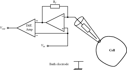
The planar patch clamp is a variation on the patch clamp where the connection to the cell is made via a micromachined aperture in a flat surface, for example a silicon substrate. The cells are sucked down onto the aperture by applying negative pressure to the electrolyte on the other side of the aperture, where an electrode is used to control the voltage and measure current as in the standard patch clamp. Use of microfabrication techniques could potentially enable mass production of identical, optimised patch clamp apertures with obvious advantages over the standard bespoke fabrication of glass pipettes which requires considerable skill. Other advantages of the planar patch clamp include the possibility of using arrays of apertures to monitor connected networks of neurons, and integration with microfluidics and microelectronics. One of the major difficulties with a planar patch clamp is achieving a reliable, high-impedance seal between the aperture and the cell. Researchers have tried various methods to ensure this, including different materials to ensure a smooth surface and the fabrication of a protruding lip but results are often inconsistent [17].
8.5.3 Extracellular Measurements of Neurons
As an alternative to intracellular and patch clamp methods, electrodes in proximity to neurons and other electroactive cells can measure behaviour such as the generation and propagation of action potential spikes. This technique measures transient potentials in the extracellular space induced by ion currents but the resulting signals are significantly weaker than those that can be measured inside cells. Therefore the method depends on the use of sensitive, low noise amplifiers and could benefit from an approach where amplification is integrated close to the measurement electrodes. For in vivo measurements the electrodes may be very fine wires of compatible metals such as platinum, stainless steel or titanium coated in a suitable insulator. The area of the electrode will depend on the diameter of the wire and how much of the insulation is removed from the tip. If the electrodes are on a similar scale to the cells they can potentially measure the activity of a single neuron, but in many cases there will be crosstalk from other cells in the vicinity.
Microelectrode arrays (MEA) are a common tool in neurophysiological research looking at cultured neuron cells or sectioned brain tissue. Typically, these are planar arrays of individually addressable electrodes capable of extracellular recording and stimulus of cells. Common systems have passively addressed arrays of over 60 electrodes, which could potentially require a measurement system with the same number of low noise amplifiers for simultaneous, multichannel recording. However, the use of multiplexing and sampling at a much faster rate than the signals of interest could obviously allow more electrodes to be measured using a single measurement system. Another alternative which would potentially allow much larger arrays of electrodes would be the integration of electronics for addressing and amplification. The main disadvantage of this, beyond the increased cost of the electrode array, is that silicon substrates are not transparent which precludes the use of an inverted microscope to view the cells.
Electrode arrays can be used to both excite action potentials and measure the response. Forcing current through the electrode can stimulate nearby cells or alternatively a voltage pulse can set up large transient currents across the electrode double-layer capacitance for a similar effect. If an action potential is induced and propagates to neurons elsewhere in the tissue section the response can be measured using other electrodes in the array.
Extracellular microelectrode array measurements typically require low-noise, voltage amplification with very low input bias currents and built in band-pass filtering to remove unwanted signals. Commercially available implementations often include separate head stage amplifiers for each electrode in the array and these may be built into the equipment used to make electrical contact to the MEA chip so that they are as close as possible.
8.1. One of the most straightforward methods of monitoring temperature is to use the thermal variation of a resistor.
8.2. A platinum based strain gauge with an unstrained resistance ( ) of 1 kΩ has a gauge factor (
 ) of 2.
 ) of 10%, what will be the maximum change in resistance (
 )? Use Equation (8.9) for the gauge factor.
 V dc?
V dc?8.3. In the following question, refer to Section 8.3.8, Figure 8.25 and Equations (8.38) to (8.42) for a half-bridge capactive sensing circuit.
 and
and  what is now the equation for the output voltage
  ?
? μm and the separation
  μm calculate the amplitude of the output voltage from the bridge when the deflection
  nm and the input voltage has an amplitude of
  V.
V.8.4. The circuit shown in Figure 8.44 is controlled by two non-overlapping clock signals as in Figure 8.28. With the help of sketches of the circuit during the two different phases, describe the operation of the amplifier and state the transfer function  .
.
Figure 8.44 Switched capacitor amplifier.
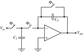
8.5. Figure 8.43 shows a circuit that could be used in patch clamp measurements of the ion current ( ) through a single ion channel.
 .
. is in the pA range suggest a suitable value for
  .
.Notes
1. Brokaw A simple three-terminal IC bandgap reference. IEEE Journal of Solid-State Circuits, 9 (6), 388–393. (1974).
2. Spark, N.T. (May 2006) A History of Murphy's Law, Periscope Film, ISBN: 978-0978638894.
3. Spark, N.T. (February 2003) The Fastest Man on Earth, Annals of Improbable Research, http://improbable.com/airchives/paperair/volume9/v9i5/murphy/murphy0.html.
4. Chaehoi, A., Begbie, M. Weiland, D. et al. (2011) Piezoresistive sensors development using monolithic CMOS MEMS technology. Sensors & Transducers Journal, 11, 1–9.
5. Lowrie, C., Desmulliez, M.P.Y. Hoff, L. et al. (2009) Fabrication of a MEMS accelerometer to detect heart bypass surgery complications. Sensor Review, 29 (4), 319–325.
6. Lowrie, C. (2010) A Three-Axis Accelerometer for Measuring Heart Wall Motion, PhD thesis, Heriot Watt University.
7. Rodahl, M., Höök, F. Krozer, A. et al. (1995) Quartz crystal microbalance setup for frequency and Q-factor measurements in gaseous and liquid environments. Review of Scientific Instruments, 66 (7), 3924.
8. Kaajakari, V. (2009) Practical MEMS, Small Gear Publishing.
9. Bracke, W., Puers, R. and Van Hoof, C. (June (2007) Ultra Low Power Capacitive Sensor Interfaces, Springer Verlag.
10. Yazdi (2004) Precision readout circuits for capacitive microaccelerometers. Sensors, 2004. Proceedings of IEEE, vol. 1, pp. 28–31.
11. Jorge, P.A.S., Caldas, P. Rosa, C.C. et al. (2004) Optical fiber probes for fluorescence based oxygen sensing. Sensors & Actuators: B. Chemical, 103 (1–2), 290–299.
12. Walker, R.J. and Richardson, J. (2011) A 12896 pixel event-driven phase-domain-based fully digital 3D camera in 0.13m CMOS imaging technology. Solid-State Circuits Conference Digest of Technical Papers (ISSCC), 2011 IEEE International, pp. 410–412.
13. Rae, B.R., Yang, J. McKendry, J. et al. (2010) A vertically integrated CMOS microsystem for time-resolved fluorescence analysis. IEEE Transactions on Biomedical Circuits and Systems, 4 (6), 437–444.
14. Buck, A.H., Campbell, C.J. Dickinson, P. et al. (2007) DNA nanoswitch as a biosensor. Analytical Chemistry, 79 (12), 4724–4728.
15. McGuinness, C.D., Nishimura, M.K.Y. Keszenman-Pereyra, D. et al. (2010) Detection of single nucleotide polymorphisms using a DNA Holliday junction nanoswitch – a high-throughput fluorescence lifetime assay. Molecular BioSystems, 6 (2), 386–390.
16. Smith, S. et al. (2012) Demonstration of a Device for Label-Free DNA Detection Through Nanoswitching. In Preparation.
17. Curtis, J.C., Baldwin, K. Dworak, B.J. et al. (2008) Seal formation in silicon planar patch-clamp microstructures. Journal of Microelectromechanical Systems, 17 (4), 974–983.
Molecular Devices (2008) or Axon Instruments (1993) The Axon Guide: A Guide to Electrophysiology & Biophysics Laboratory Techniques, Various editions available online.
Standen, N.B., Gray, P.T.A. and Whitaker, M.J. (eds) (1994) Microelectrode Techniques. The Plymouth Workshop Handbook, Company of Biologists, ISBN: 978-0948601491.