Chapter 4
Computing Platforms
Chapter Points
• CPU buses, I/O devices, and interfacing.
• The CPU system as a framework for understanding design methodology.
• System-level performance and power consumption.
4.1 Introduction
In this chapter, we concentrate on computing platforms created using microprocessors, I/O devices, and memory components. The microprocessor is an important element of the embedded computing system, but it cannot do its job without memories and I/O devices. We need to understand how to interconnect microprocessors and devices using the CPU bus. The application also relies on software that is closely tied to the platform hardware. Luckily, there are many similarities between the platforms required for different applications, so we can extract some generally useful principles by examining a few basic concepts.
The next section surveys the landscape in computing platforms including both hardware and software. Section 4.3 discusses CPU buses. Section 4.4 describes memory components. Section 4.5 considers how to design with computing platforms. Section 4.6 looks at consumer electronics devices as an example of computing platforms, the requirements on them, and some important components. Section 4.7 develops methods to analyze performance at the platform level. We close with two design examples: an alarm clock in Section 4.8 and a portable audio player in Section 4.9.
4.2 Basic Computing Platforms
While some embedded systems require sophisticated platforms, many can be built around the variations of a generic computer system ranging from 4-bit microprocessors through complex systems-on-chips. The platform provides the environment in which we can develop our embedded application. It encompasses both hardware and software components—one without the other is generally not very useful.
4.2.1 Platform Hardware Components
We are familiar with the CPU and memory as an idealized computer system. A practical computer needs additional components. As shown in Figure 4.1, a typical computing platform includes several major hardware components:
• The CPU provides basic computational facilities.
• RAM is used for program and data storage.
• ROM holds the boot program and some permanent data.
• A DMA controller provides direct memory access capabilities.
• Timers are used by the operating system for a variety of purposes.
• A high-speed bus, connected to the CPU bus through a bridge, allows fast devices to communicate efficiently with the rest of the system.
• A low-speed bus provides an inexpensive way to connect simpler devices and may be necessary for backward compatibility as well.
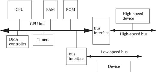
Figure 4.1 Hardware architecture of a typical computing platform.
Buses
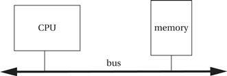
The bus provides a common connection between all the components in the computer: the CPU, memories, and I/O devices. We will discuss buses in more detail in Section 4.3; the bus transmits addresses, data, and control information so that one device on the bus can read or write another device.
While very simple systems will have only one bus, more complex platforms may have several buses. Buses are often classified by their overall performance: low-speed, high-speed, etc. Multiple buses serve two purposes. First, devices on different buses will interact much less than those on the same bus. Dividing the devices between buses can help reduce the overall load and increase the utilization of the buses. Second, low-speed buses usually provide simpler and cheaper interfaces than do high-speed buses. A low-speed device may not benefit from the effort required to connect it to a high-speed bus.
A wide range of buses are used in computer systems. The Universal Serial Bus (USB), for example, is a bus that uses a small bundle of serial connections. For a serial bus, USB provides high performance. However, complex buses such as PCI may use many parallel connections and other techniques to provide higher absolute performance.
Access patterns
Data transfers may occur between many pairs of components: CPU to/from memory, CPU to/from I/O device, memory to memory, or I/O to I/O device. Because the bus connects all these components (possibly through a bridge), it can mediate all types of transfers. However, the basic data transfer requires executing instructions on the CPU. We can use a direct memory access (DMA) unit to offload some of the work of basic transfers. We will discuss DMA in more detail in Section 4.3.
Single-chip platforms
We can also put all the components for a basic computing platform on a single chip. A single-chip platform makes the development of certain types of embedded systems much easier, providing the rich software development of a PC with the low cost of a single-chip hardware platform. The ability to integrate a CPU and devices on a single chip has allowed manufacturers to provide single-chip systems that do not conform to board-level standards.
Microcontrollers
The term microcontroller refers to a single chip that includes a CPU, memory, and I/O devices. The term was originally used for platforms based on small 4-bit and 8-bit processors but can also refer to single-chip systems using large processors as well.
The next two examples look at two different single-chip systems. Application Example 4.1 looks at the PIC16F882 while Application Example 4.2 describes the Intel StrongARM SA-1100.
Application Example 4.1 System Organization of the PIC16F882
Here is the block diagram of the PIC16F882 (as well as the 883 and 886) microcontroller [Mic09]:
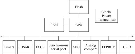
PIC is a Harvard architecture; the flash memory used for instructions is accessible only to the CPU. The flash memory can be programmed using separate mechanisms. The microcontroller includes a number of devices: timers, a universal synchronous/asynchronous receiver/transmitter (EUSART); capture-and-compare (ECCP) modules; a master synchronous serial port; an analog-to-digital converter (ADC); analog comparators and references; an electrically erasable PROM (EEPROM); and general-purpose I/O (GPIO).
Application Example 4.2 System Organization of the Intel StrongARM SA-1100 and SA-1111
The StrongARM SA-1100 provides a number of functions besides the ARM CPU:
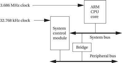
The chip contains two on-chip buses: a high-speed system bus and a lower-speed peripheral bus. The chip also uses two different clocks. A 3.686-MHz clock is used to drive the CPU and high-speed peripherals, and a 32.768-kHz clock is an input to the system control module. The system control module contains the following peripheral devices:
The 32.768-kHz clock’s frequency is chosen to be useful in timing real-time events. The slower clock is also used by the power manager to provide continued operation of the manager at a lower clock rate and therefore lower power consumption.
The SA-1111 is a companion chip that provides a suite of I/O functions. It connects to the SA-1100 through its system bus and provides several functions: a USB host controller; PS/2 ports for keyboards, mice, and so on; a PCMCIA interface; pulse-width modulation outputs; a serial port for digital audio; and an SSP serial port for telecom interfacing.
4.2.2 Platform Software Components
Hardware and software are inseparable—each needs the other to perform its function. Much of the software in an embedded system will come from outside sources. Some software components may come from third parties. Hardware vendors generally provide a basic set of software platform components to encourage use of their hardware. These components range across many layers of abstraction.
Layer diagrams are often used to describe the relationships between different software components in a system. Figure 4.2 shows a layer diagram for an embedded system. The hardware abstraction layer (HAL) provides a basic level of abstraction from the hardware. Device drivers often use the HAL to simplify their structure. Similarly, the power management module must have low-level access to hardware. The operating system and file system provide the basic abstractions required to build complex applications. Because many embedded systems are algorithm-intensive, we often make use of library routines to perform complex kernel functions. These routines may be developed internally and reused or, in many cases, they come from the manufacturer and are heavily optimized for the hardware platform. The application makes use of all these layers, either directly or indirectly.
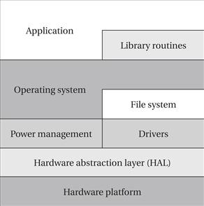
Figure 4.2 Software layer diagram for an embedded system.
4.3 The CPU Bus
The bus is the mechanism by which the CPU communicates with memory and devices. A bus is, at a minimum, a collection of wires but it also defines a protocol by which the CPU, memory, and devices communicate. One of the major roles of the bus is to provide an interface to memory. (Of course, I/O devices also connect to the bus.) Based on understanding of the bus, we study the characteristics of memory components in this section, focusing on DMA. We will also look at how buses are used in computer systems.
4.3.1 Bus Organization and Protocol
A bus is a common connection between components in a system. As shown in Figure 4.3, the CPU, memory, and I/O devices are all connected to the bus. The signals that make up the bus provide the necessary communication: the data itself, addresses, a clock, and some control signals.
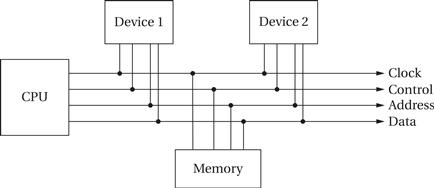
Figure 4.3 Organization of a bus.
Bus master
In a typical bus system, the CPU serves as the bus master and initiates all transfers. If any device could request a transfer, then other devices might be starved of bus bandwidth. As bus master, the CPU reads and writes data and instructions from memory. It also initiates all reads or writes on I/O devices. We will see shortly that DMA allows other devices to temporarily become the bus master and transfer data without the CPU’s involvement.
Four-cycle handshake
The basic building block of most bus protocols is the four-cycle handshake, illustrated in Figure 4.4. The handshake ensures that when two devices want to communicate, one is ready to transmit and the other is ready to receive. The handshake uses a pair of wires dedicated to the handshake: enq (meaning enquiry) and ack (meaning acknowledge). Extra wires are used for the data transmitted during the handshake. Each step in the handshake is identified by a transition on enq or ack:
1. Device 1 raises its output to signal an enquiry, which tells device 2 that it should get ready to listen for data.
2. When device 2 is ready to receive, it raises its output to signal an acknowledgment. At this point, devices 1 and 2 can transmit or receive.
3. Once the data transfer is complete, device 2 lowers its output, signaling that it has received the data.
4. After seeing that ack has been released, device 1 lowers its output.
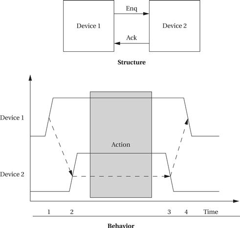
Figure 4.4 The four-cycle handshake.
At the end of the handshake, both handshaking signals are low, just as they were at the start of the handshake. The system has thus returned to its original state in readiness for another handshake-enabled data transfer.
Bus signals
Microprocessor buses build on the handshake for communication between the CPU and other system components. The term bus is used in two ways. The most basic use is as a set of related wires, such as address wires. However, the term may also mean a protocol for communicating between components. To avoid confusion, we will use the term bundle to refer to a set of related signals. The fundamental bus operations are reading and writing. The major components on a typical bus include:
• Clock provides synchronization to the bus components;
• R/W’ is true when the bus is reading and false when the bus is writing;
• Address is an a-bit bundle of signals that transmits the address for an access;
• Data is an n-bit bundle of signals that can carry data to or from the CPU; and
• Data ready signals when the values on the data bundle are valid.
All transfers on this basic bus are controlled by the CPU—the CPU can read or write a device or memory, but devices or memory cannot initiate a transfer. This is reflected by the fact that R/W’ and address are unidirectional signals, because only the CPU can determine the address and direction of the transfer.
Bus reads and writes
Figure 4.5 shows a sequence diagram for a read followed by a write. The CPU first reads a location from memory and then writes it to dev1. The bus mediates each transfer. The bus operates under a protocol that determines when components on the bus can use certain signals and what those signals mean. The details of bus protocols are not important here. But it is important to keep in mind that bus operations take time; the clock frequency of the bus is often much lower than that of the CPU. We will see how to analyze platform-level performance in Section 4.7.
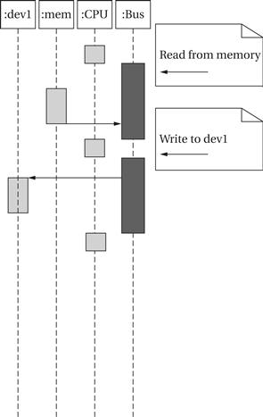
Figure 4.5 A typical sequence diagram for bus operations.
Sequence diagrams don’t give us enough detail to fully understand the hardware. To provide the required detail, the behavior of a bus is most often specified as a timing diagram. A timing diagram shows how the signals on a bus vary over time, but because values like the address and data can take on many values, some standard notation is used to describe signals, as shown in Figure 4.6. A’s value is known at all times, so it is shown as a standard waveform that changes between zero and one. B and C alternate between changing and stable states. A stable signal has, as the name implies, a stable value that could be measured by an oscilloscope, but the exact value of that signal does not matter for purposes of the timing diagram. For example, an address bus may be shown as stable when the address is present, but the bus’s timing requirements are independent of the exact address on the bus. A signal can go between a known 0/1 state and a stable/changing state. A changing signal does not have a stable value. Changing signals should not be used for computation. To be sure that signals go to their proper values at the proper times, timing diagrams sometimes show timing constraints. We draw timing constraints in two different ways, depending on whether we are concerned with the amount of time between events or only the order of events. The timing constraint from A to B, for example, shows that A must go high before B becomes stable. The constraint from A to B also has a time value of 10 ns, indicating that A goes high at least 10 ns before B goes stable.
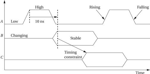
Figure 4.6 Timing diagram notation.
Figure 4.7 shows a timing diagram for the example bus. The diagram shows a read followed by a write. Timing constraints are shown only for the read operation, but similar constraints apply to the write operation. The bus is normally in the read mode because that does not change the state of any of the devices or memories. The CPU can then ignore the bus data lines until it wants to use the results of a read. Notice also that the direction of data transfer on bidirectional lines is not specified in the timing diagram. During a read, the external device or memory is sending a value on the data lines, while during a write the CPU is controlling the data lines.
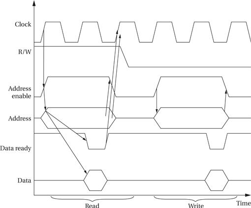
Figure 4.7 Timing diagram for read and write on the example bus.
With practice, we can see the sequence of operations for a read on the timing diagram:
• A read or write is initiated by setting address enable high after the clock starts to rise. We set R/W = 1 to indicate a read, and the address lines are set to the desired address.
• One clock cycle later, the memory or device is expected to assert the data value at that address on the data lines. Simultaneously, the external device specifies that the data are valid by pulling down the data ready line. This line is active low, meaning that a logically true value is indicated by a low voltage, in order to provide increased immunity to electrical noise.
• The CPU is free to remove the address at the end of the clock cycle and must do so before the beginning of the next cycle. The external device has a similar requirement for removing the data value from the data lines.
The write operation has a similar timing structure. The read/write sequence illustrates that timing constraints are required on the transition of the R/W signal between read and write states. The signal must, of course, remain stable within a read or write. As a result there is a restricted time window in which the CPU can change between read and write modes.
The handshake that tells the CPU and devices when data are to be transferred is formed by data ready for the acknowledge side, but is implicit for the enquiry side. Because the bus is normally in read mode, enq does not need to be asserted, but the acknowledge must be provided by data ready.
The data ready signal allows the bus to be connected to devices that are slower than the bus. As shown in Figure 4.8, the external device need not immediately assert data ready. The cycles between the minimum time at which data can be asserted and when it is actually asserted are known as wait states. Wait states are commonly used to connect slow, inexpensive memories to buses.
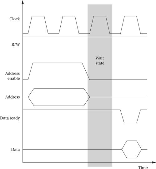
Figure 4.8 A wait state on a read operation.
We can also use the bus handshaking signals to perform burst transfers, as illustrated in Figure 4.9. In this burst read transaction, the CPU sends one address but receives a sequence of data values. We add an extra line to the bus, called burst’ here, which signals when a transaction is actually a burst. Releasing the burst’ signal tells the device that enough data has been transmitted. To stop receiving data after the end of data 4, the CPU releases the burst’ signal at the end of data 3 because the device requires some time to recognize the end of the burst. Those values come from successive memory locations starting at the given address.
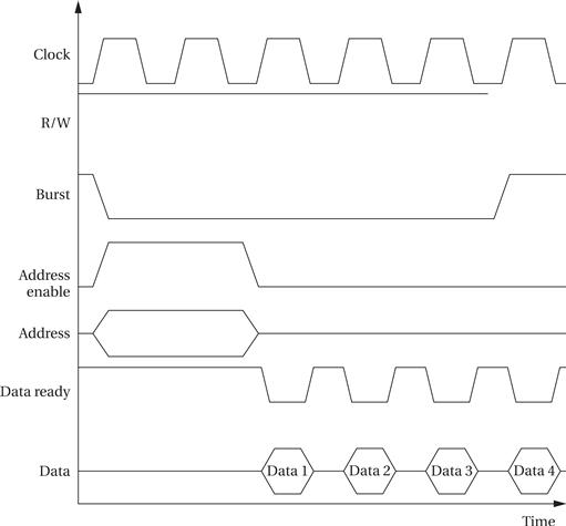
Figure 4.9 A burst read transaction.
Some buses provide disconnected transfers. In these buses, the request and response are separate. A first operation requests the transfer. The bus can then be used for other operations. The transfer is completed later, when the data are ready.
The state machine view of the bus transaction is also helpful and a useful complement to the timing diagram. Figure 4.10 shows the CPU and device state machines for the read operation. As with a timing diagram, we do not show all the possible values of address and data lines but instead concentrate on the transitions of control signals. When the CPU decides to perform a read transaction, it moves to a new state, sending bus signals that cause the device to behave appropriately. The device’s state transition graph captures its side of the protocol.
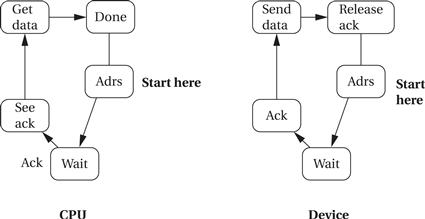
Figure 4.10 State diagrams for the bus read transaction.
Some buses have data bundles that are smaller than the natural word size of the CPU. Using fewer data lines reduces the cost of the chip. Such buses are easiest to design when the CPU is natively addressable. A more complicated protocol hides the smaller data sizes from the instruction execution unit in the CPU. Byte addresses are sequentially sent over the bus, receiving one byte at a time; the bytes are assembled inside the CPU’s bus logic before being presented to the CPU proper.
4.3.2 DMA
Standard bus transactions require the CPU to be in the middle of every read and write transaction. However, there are certain types of data transfers in which the CPU does not need to be involved. For example, a high-speed I/O device may want to transfer a block of data into memory. While it is possible to write a program that alternately reads the device and writes to memory, it would be faster to eliminate the CPU’s involvement and let the device and memory communicate directly. This capability requires that some unit other than the CPU be able to control operations on the bus.
Direct memory access (DMA) is a bus operation that allows reads and writes not controlled by the CPU. A DMA transfer is controlled by a DMA controller, which requests control of the bus from the CPU. After gaining control, the DMA controller performs read and write operations directly between devices and memory.
Figure 4.11 shows the configuration of a bus with a DMA controller. The DMA requires the CPU to provide two additional bus signals:
• The bus request is an input to the CPU through which DMA controllers ask for ownership of the bus.
• The bus grant signals that the bus has been granted to the DMA controller.
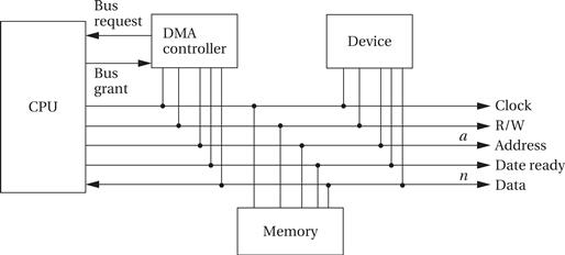
Figure 4.11 A bus with a DMA controller.
The DMA controller can act as a bus master. It uses the bus request and bus grant signal to gain control of the bus using a classic four-cycle handshake. A bus request is asserted by the DMA controller when it wants to control the bus, and the bus grant is asserted by the CPU when the bus is ready. The CPU will finish all pending bus transactions before granting control of the bus to the DMA controller. When it does grant control, it stops driving the other bus signals: R/W, address, and so on. Upon becoming bus master, the DMA controller has control of all bus signals (except, of course, for bus request and bus grant).
Once the DMA controller is bus master, it can perform reads and writes using the same bus protocol as with any CPU-driven bus transaction. Memory and devices do not know whether a read or write is performed by the CPU or by a DMA controller. After the transaction is finished, the DMA controller returns the bus to the CPU by deasserting the bus request, causing the CPU to de-assert the bus grant.
The CPU controls the DMA operation through registers in the DMA controller. A typical DMA controller includes the following three registers:
• A starting address register specifies where the transfer is to begin.
• A length register specifies the number of words to be transferred.
• A status register allows the DMA controller to be operated by the CPU.
The CPU initiates a DMA transfer by setting the starting address and length registers appropriately and then writing the status register to set its start transfer bit. After the DMA operation is complete, the DMA controller interrupts the CPU to tell it that the transfer is done.
Concurrency during DMA
What is the CPU doing during a DMA transfer? It cannot use the bus. As illustrated in Figure 4.12, if the CPU has enough instructions and data in the cache and registers, it may be able to continue doing useful work for quite some time and may not notice the DMA transfer. But once the CPU needs the bus, it stalls until the DMA controller returns bus mastership to the CPU.
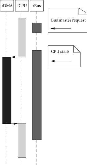
Figure 4.12 UML sequence of system activity around a DMA transfer.
To prevent the CPU from idling for too long, most DMA controllers implement modes that occupy the bus for only a few cycles at a time. For example, the transfer may be made 4, 8, or 16 words at a time. As illustrated in Figure 4.13, after each block, the DMA controller returns control of the bus to the CPU and goes to sleep for a preset period, after which it requests the bus again for the next block transfer.
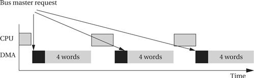
Figure 4.13 Cyclic scheduling of a DMA request.
4.3.3 System Bus Configurations
A microprocessor system often has more than one bus. As shown in Figure 4.14, high-speed devices may be connected to a high-performance bus, while lower-speed devices are connected to a different bus. A small block of logic known as a bridge allows the buses to connect to each other. There are three reasons to do this:
• Higher-speed buses may provide wider data connections.
• A high-speed bus usually requires more expensive circuits and connectors. The cost of low-speed devices can be held down by using a lower-speed, lower-cost bus.
• The bridge may allow the buses to operate independently, thereby providing some parallelism in I/O operations.
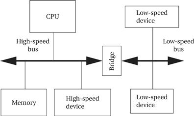
Figure 4.14 A multiple bus system.
Bus bridges
Let’s consider the operation of a bus bridge between what we will call a fast bus and a slow bus as illustrated in Figure 4.15. The bridge is a slave on the fast bus and the master of the slow bus. The bridge takes commands from the fast bus on which it is a slave and issues those commands on the slow bus. It also returns the results from the slow bus to the fast bus—for example, it returns the results of a read on the slow bus to the fast bus.
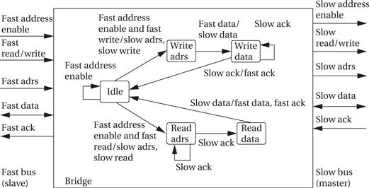
Figure 4.15 UML state diagram of bus bridge operation.
The upper sequence of states handles a write from the fast bus to the slow bus. These states must read the data from the fast bus and set up the handshake for the slow bus. Operations on the fast and slow sides of the bus bridge should be overlapped as much as possible to reduce the latency of bus-to-bus transfers. Similarly, the bottom sequence of states reads from the slow bus and writes the data to the fast bus.
The bridge serves as a protocol translator between the two bridges as well. If the bridges are very close in protocol operation and speed, a simple state machine may be enough. If there are larger differences in the protocol and timing between the two buses, the bridge may need to use registers to hold some data values temporarily.
ARM bus
Because the ARM CPU is manufactured by many different vendors, the bus provided off-chip can vary from chip to chip. ARM has created a separate bus specification for single-chip systems. The AMBA bus [ARM99A] supports CPUs, memories, and peripherals integrated in a system-on-silicon. As shown in Figure 4.16, the AMBA specification includes two buses. The AMBA high-performance bus (AHB) is optimized for high-speed transfers and is directly connected to the CPU. It supports several high-performance features: pipelining, burst transfers, split transactions, and multiple bus masters.
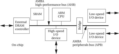
Figure 4.16 Elements of the ARM AMBA bus system.
A bridge can be used to connect the AHB to an AMBA peripherals bus (APB). This bus is designed to be simple and easy to implement; it also consumes relatively little power. The APB assumes that all peripherals act as slaves, simplifying the logic required in both the peripherals and the bus controller. It also does not perform pipelined operations, which simplifies the bus logic.
4.4 Memory Devices and Systems
Random-access memories can be both read and written. They are called random access because, unlike magnetic disks, addresses can be read in any order. Most bulk memory in modern systems is dynamic RAM (DRAM). DRAM is very dense; it does, however, require that its values be refreshed periodically because the values inside the memory cells decay over time.
Basic DRAM organization
Although the basic organization of memories is simple, a number of variations exist that provide different trade-offs [Cup01]. As shown in Figure 4.17, a simple memory is organized as a two-dimensional array. Assume for the moment that the memory is accessed one bit at a time. The address for that bit is split into two sections: row and column. Together they form a complete location in the array. If we want to access more than one bit at a time, we can use fewer bits in the column part of the address to select several columns simultaneously. The division of an address into rows and columns is important because it is reflected at the pins of the memory chip and so is visible to the rest of the system. In a traditional DRAM, the row is sent first followed by the column. Two control signals tell the DRAM when those address bits are valid: not Row Address Select or RAS’ and not Column Address Select or CAS’.
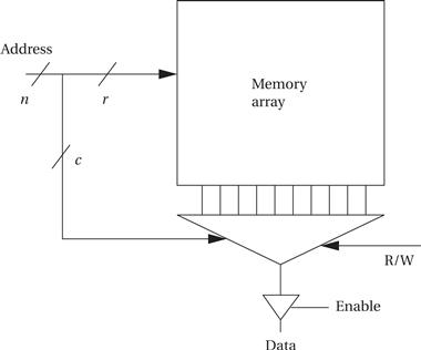
Figure 4.17 Organization of a basic memory.
Refreshing
DRAM has to be refreshed periodically to retain its values. Rather than refresh the entire memory at once, DRAMs refresh part of the memory at a time. When a section of memory is being refreshed, it can’t be accessed until the refresh is complete. The memory refresh occurs over fairly small seconds so that each section is refreshed every few microseconds.
Bursts and page mode
Memories may offer some special modes that reduce the time required for accesses. Bursts and page mode accesses are both more efficient forms of accesses but differ in how they work. Burst transfers perform several accesses in sequence using a single address and possibly a single CAS signal. Page mode, in contrast, requires a separate address for each data access.
Types of DRAM
Many types of DRAM are available. Each has its own characteristics, usually centering on how the memory is accessed. Some examples include:
Synchronous dynamic RAM
SDRAMs use RAS’ and CAS’ signals to break the address into two parts, which select the proper row and column in the RAM array. Signal transitions are relative to the SDRAM clock, which allows the internal SDRAM operations to be pipelined. As shown in Figure 4.18, transitions on the control signals are related to a clock [Mic00]. SDRAMs include registers that control the mode in which the SDRAM operates. SDRAMs support burst modes that allow several sequential addresses to be accessed by sending only one address. SDRAMs generally also support an interleaved mode that exchanges pairs of bytes.
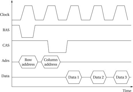
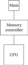
Figure 4.18 An SDRAM read operation.
Figure 4.19 The memory controller in a computer system.
Memory packaging
Memory for PCs is generally purchased as single in-line memory modules (SIMMs) or double in-line memory modules (DIMMs). A SIMM or DIMM is a small circuit board that fits into a standard memory socket. A DIMM has two sets of leads compared to the SIMM’s one. Memory chips are soldered to the circuit board to supply the desired memory.
Read-only memories (ROMs) are preprogrammed with fixed data. They are very useful in embedded systems because a great deal of the code, and perhaps some data, does not change over time. Flash memory is the dominant form of ROM. Flash memory can be erased and rewritten using standard system voltages, allowing it to be reprogrammed inside a typical system. This allows applications such as automatic distribution of upgrades—the flash memory can be reprogrammed while downloading the new memory contents from a telephone line. Early flash memories had to be erased in their entirety; modern devices allow memory to be erased in blocks. Most flash memories today allow certain blocks to be protected. A common application is to keep the boot-up code in a protected block but allow updates to other memory blocks on the device. As a result, this form of flash is commonly known as boot-block flash.
4.4.1 Memory System Organization
A modern memory is more than a 1-dimensional array of bits. Memory chips have surprisingly complex organizations that allow us to make some useful optimizations. For example, memories are usually often divided into several smaller memory arrays.
Memory controllers
Modern computer systems use a memory controller as the interface between the CPU and the memory components. As shown in Figure 4.19, the memory controller shields the CPU from knowledge of the detailed timing of different memory components. If the memory also consists of several different components, the controller will manage all the accesses to all memories. Memory accesses must be scheduled. The memory controller will receive a sequence of requests from the processor. However, it may not be possible to execute them as quickly as they are received if the memory component is already processing an access. When faced with more accesses than resources available to complete them, the memory controller will determine the order in which they will be handled and schedule the accesses accordingly.
Channels and banks
Channels and banks are two ways to add parallelism to the memory system. A channel is a connection to a group of memory components. If the CPU and memory controller can support multiple channels that operate concurrently, then we can perform multiple independent accesses using the different channels. We may also divide the complete memory system into banks. Banks can perform accesses in parallel because each has its own memory arrays and addressing logic. By properly arranging memory into banks, we can overlap some of the access time for these locations and reduce the total time required for the complete set of accesses.
Figure 4.20 shows a memory system organized into channels and banks. Each channel has its own memory components and its own connection to the processor. Channels operate completely separately. The memory in each channel can be subdivided into banks. The banks in a channel can be accessed separately. Channels are in general more expensive than banks. A two-channel memory system, for example, requires twice as many pins and wires connecting the CPU and memory as does a one-channel system. Memory components are often separated internally into banks and providing that access to the outside is less expensive.
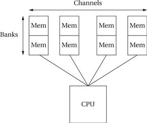
Figure 4.20 Channels and banks in a memory system.
4.5 Designing with Computing Platforms
In this section we concentrate on how to create a working embedded system based on a computing platform. We will first look at some example platforms and what they include. We will then consider how to choose a platform for an application and how to make effective use of the chosen platform.
4.5.1 Example Platforms
The design complexity of the hardware platform can vary greatly, from a totally off-the-shelf solution to a highly customized design. A platform may consist of anywhere from one to dozens of chips.
Open source platforms
Figure 4.21 shows a BeagleBoard [Bea11]. The BeagleBoard is the result of an open source project to develop a low-cost platform for embedded system projects. The processor is an ARM Cortex™-A8, which also comes with several built-in I/O devices. The board itself includes many connectors and support for a variety of I/O: flash memory, audio, video, etc. The support environment provides basic information about the board design such as schematics, a variety of software development environments, and many example projects built with the BeagleBoard.
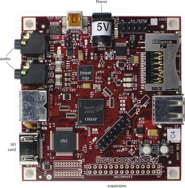
Figure 4.21 A BeagleBoard.
Evaluation boards
Chip vendors often provide their own evaluation boards or evaluation modules for their chips. The evaluation board may be a complete solution or provide what you need with only slight modifications. The hardware design (netlist, board layout, etc.) is typically available from the vendor; companies provide such information to make it easy for customers to use their microprocessors. If the evaluation board does not completely meet your needs, you can modify the design using the netlist and board layout without starting from scratch. Vendors generally do not charge royalties for the hardware board design.
Figure 4.22 shows an ARM evaluation module. Like the BeagleBoard, this evaluation module includes the basic platform chip and a variety of I/O devices. However, the main purpose of the BeagleBoard is as an end-use, low-cost board, while the evaluation module is primarily intended to support software development and serve as a starting point for a more refined product design. As a result, this evaluation module includes some features that would not appear in a final product such as the connections to the processor’s pins that surround the processor chip itself.
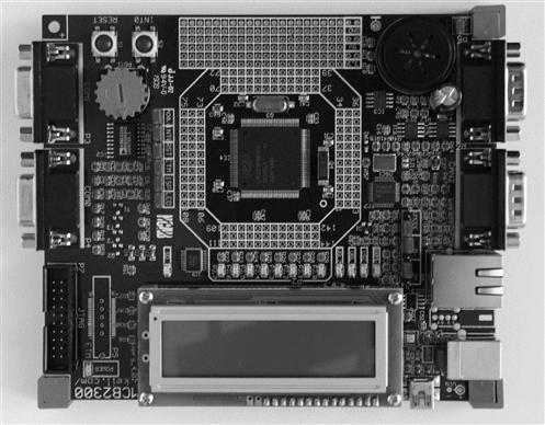
Figure 4.22 An ARM evaluation module.
4.5.2 Choosing a Platform
We probably will not design the platform for our embedded system from scratch. We may assemble hardware and software components from several sources; we may also acquire a complete hardware/software platform package. A number of factors will contribute to your decision to use a particular platform.
Hardware
The hardware architecture of the platform is the more obvious manifestation of the architecture because you can touch it and feel it. The various components may all play a factor in the suitability of the platform.
• CPU: An embedded computing system clearly contains a microprocessor. But which one? There are many different architectures, and even within an architecture we can select between models that vary in clock speed, bus data width, integrated peripherals, and so on. The choice of the CPU is one of the most important, but it cannot be made without considering the software that will execute on the machine.
• Bus: The choice of a bus is closely tied to that of a CPU, because the bus is an integral part of the microprocessor. But in applications that make intensive use of the bus due to I/O or other data traffic, the bus may be more of a limiting factor than the CPU. Attention must be paid to the required data bandwidths to be sure that the bus can handle the traffic.
• Memory: Once again, the question is not whether the system will have memory but the characteristics of that memory. The most obvious characteristic is total size, which depends on both the required data volume and the size of the program instructions. The ratio of ROM to RAM and selection of DRAM versus SRAM can have a significant influence on the cost of the system. The speed of the memory will play a large part in determining system performance.
• Input and output devices: If we use a platform built out of many low-level components on a printed circuit board, we may have a great deal of freedom in the I/O devices connected to the system. Platforms based on highly integrated chips only come with certain combinations of I/O devices. The combination of I/O devices available may be a prime factor in platform selection. We may need to choose a platform that includes some I/O devices we do not need in order to get the devices that we do need.
Software
When we think about software components of the platform, we generally think about both the run-time components and the support components. Run-time components become part of the final system: the operating system, code libraries, and so on. Support components include the code development environment, debugging tools, and so on.
Run-time components are a critical part of the platform. An operating system is required to control the CPU and its multiple processes. A file system is used in many embedded systems to organize internal data and as an interface to other systems. Many complex libraries—digital filtering and FFT—provide highly optimized versions of complex functions.
Support components are critical to making use of complex hardware platforms. Without proper code development and operating systems, the hardware itself is useless. Tools may come directly from the hardware vendor, from third-party vendors, or from developer communities.
4.5.3 Intellectual Property
Intellectual property (IP) is something that we can own but not touch: software, netlists, and so on. Just as we need to acquire hardware components to build our system, we also need to acquire intellectual property to make that hardware useful. Here are some examples of the wide range of IP that we use in embedded system design:
• run-time software libraries;
• software development environments;
• schematics, netlists, and other hardware design information.
IP can come from many different sources. We may buy IP components from vendors. For example, we may buy a software library to perform certain complex functions and incorporate that code into our system. We may also obtain it from developer communities on-line.
Example 4.1 looks at the IP available for the BeagleBoard.
Example 4.1 BeagleBoard Intellectual Property
The BeagleBoard Web site (http://www.beagleboard.org) contains both hardware and software IP. Hardware IP includes:
• schematics for the printed circuit board;
• artwork files (known as Gerber files) for the printed circuit board;
Software IP includes:
4.5.4 Development Environments
Although we may use an evaluation board, much of the software development for an embedded system is done on a PC or workstation known as a host as illustrated in Figure 4.23. The hardware on which the code will finally run is known as the target. The host and target are frequently connected by a USB link, but a higher-speed link such as Ethernet can also be used.
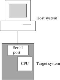
Figure 4.23 Connecting a host and target system.
The target must include a small amount of software to talk to the host system. That software will take up some memory, interrupt vectors, and so on, but it should generally leave the smallest possible footprint in the target to avoid interfering with the application software. The host should be able to do the following:
A cross-compiler is a compiler that runs on one type of machine but generates code for another. After compilation, the executable code is typically downloaded to the embedded system by USB. We also often make use of host-target debuggers, in which the basic hooks for debugging are provided by the target and a more sophisticated user interface is created by the host.
We often create a testbench program that can be built to help debug embedded code. The testbench generates inputs to stimulate a piece of code and compares the outputs against expected values, providing valuable early debugging help. The embedded code may need to be slightly modified to work with the testbench, but careful coding (such as using the #ifdef directive in C) can ensure that the changes can be undone easily and without introducing bugs.
4.5.5 Debugging Techniques
A good deal of software debugging can be done by compiling and executing the code on a PC or workstation. But at some point it inevitably becomes necessary to run code on the embedded hardware platform. Embedded systems are usually less friendly programming environments than PCs. Nonetheless, the resourceful designer has several options available for debugging the system.
The USB port found on most evaluation boards is one of the most important debugging tools. In fact, it is often a good idea to design a USB port into an embedded system even if it will not be used in the final product; USB can be used not only for development debugging but also for diagnosing problems in the field or field upgrades of software.
Another very important debugging tool is the breakpoint. The simplest form of a breakpoint is for the user to specify an address at which the program’s execution is to break. When the PC reaches that address, control is returned to the monitor program. From the monitor program, the user can examine and/or modify CPU registers, after which execution can be continued. Implementing breakpoints does not require using exceptions or external devices.
Programming Example 4.1 shows how to use instructions to create breakpoints.
Programming Example 4.1 Breakpoints
A breakpoint is a location in memory at which a program stops executing and returns to the debugging tool or monitor program. Implementing breakpoints is very simple—you simply replace the instruction at the breakpoint location with a subroutine call to the monitor. In the following code, to establish a breakpoint at location 0 × 40c in some ARM code, we’ve replaced the branch (B) instruction normally held at that location with a subroutine call (BL) to the breakpoint handling routine:
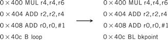
When the breakpoint handler is called, it saves all the registers and can then display the CPU state to the user and take commands.
To continue execution, the original instruction must be replaced in the program. If the breakpoint can be erased, the original instruction can simply be replaced and control returned to that instruction. This will normally require fixing the subroutine return address, which will point to the instruction after the breakpoint. If the breakpoint is to remain, then the original instruction can be replaced and a new temporary breakpoint placed at the next instruction (taking jumps into account, of course). When the temporary breakpoint is reached, the monitor puts back the original breakpoint, removes the temporary one, and resumes execution.
The Unix dbx debugger shows the program being debugged in source code form, but that capability is too complex to fit into most embedded systems. Very simple monitors will require you to specify the breakpoint as an absolute address, which requires you to know how the program was linked. A more sophisticated monitor will read the symbol table and allow you to use labels in the assembly code to specify locations.
LEDs as debugging devices
Never underestimate the importance of LEDs (light-emitting diodes) in debugging. As with serial ports, it is often a good idea to design in a few to indicate the system state even if they will not normally be seen in use. LEDs can be used to show error conditions, when the code enters certain routines, or to show idle time activity. LEDs can be entertaining as well—a simple flashing LED can provide a great sense of accomplishment when it first starts to work.
In-circuit emulation
When software tools are insufficient to debug the system, hardware aids can be deployed to give a clearer view of what is happening when the system is running. The microprocessor in-circuit emulator (ICE) is a specialized hardware tool that can help debug software in a working embedded system. At the heart of an in-circuit emulator is a special version of the microprocessor that allows its internal registers to be read out when it is stopped. The in-circuit emulator surrounds this specialized microprocessor with additional logic that allows the user to specify breakpoints and examine and modify the CPU state. The CPU provides as much debugging functionality as a debugger within a monitor program, but does not take up any memory. The main drawback to in-circuit emulation is that the machine is specific to a particular microprocessor, even down to the pinout. If you use several microprocessors, maintaining a fleet of in-circuit emulators to match can be very expensive.
Logic analyzers
The logic analyzer[Ald73] is the other major piece of instrumentation in the embedded system designer’s arsenal. Think of a logic analyzer as an array of inexpensive oscilloscopes—the analyzer can sample many different signals simultaneously (tens to hundreds) but can display only 0, 1, or changing values for each. All these logic analysis channels can be connected to the system to record the activity on many signals simultaneously. The logic analyzer records the values on the signals into an internal memory and then displays the results on a display once the memory is full or the run is aborted. The logic analyzer can capture thousands or even millions of samples of data on all of these channels, providing a much larger time window into the operation of the machine than is possible with a conventional oscilloscope.
A typical logic analyzer can acquire data in either of two modes that are typically called state and timing modes. To understand why two modes are useful and the difference between them, it is important to remember that an oscilloscope trades reduced resolution on the signals for the longer time window. The measurement resolution on each signal is reduced in both voltage and time dimensions. The reduced voltage resolution is accomplished by measuring logic values (0, 1, x) rather than analog voltages. The reduction in timing resolution is accomplished by sampling the signal, rather than capturing a continuous waveform as in an analog oscilloscope.
State and timing mode represent different ways of sampling the values. Timing mode uses an internal clock that is fast enough to take several samples per clock period in a typical system. State mode, on the other hand, uses the system’s own clock to control sampling, so it samples each signal only once per clock cycle. As a result, timing mode requires more memory to store a given number of system clock cycles. On the other hand, it provides greater resolution in the signal for detecting glitches. Timing mode is typically used for glitch-oriented debugging, while state mode is used for sequentially oriented problems.
The internal architecture of a logic analyzer is shown in Figure 4.24. The system’s data signals are sampled at a latch within the logic analyzer; the latch is controlled by either the system clock or the internal logic analyzer sampling clock, depending on whether the analyzer is being used in state or timing mode. Each sample is copied into a vector memory under the control of a state machine. The latch, timing circuitry, sample memory, and controller must be designed to run at high speed because several samples per system clock cycle may be required in timing mode. After the sampling is complete, an embedded microprocessor takes over to control the display of the data captured in the sample memory.
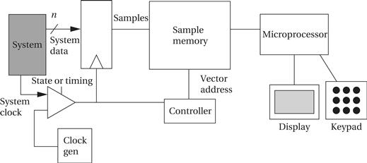
Figure 4.24 Architecture of a logic analyzer.
Logic analyzers typically provide a number of formats for viewing data. One format is a timing diagram format. Many logic analyzers allow not only customized displays, such as giving names to signals, but also more advanced display options. For example, an inverse assembler can be used to turn vector values into microprocessor instructions. The logic analyzer does not provide access to the internal state of the components, but it does give a very good view of the externally visible signals. That information can be used for both functional and timing debugging.
4.5.6 Debugging Challenges
Logical errors in software can be hard to track down, but errors in real-time code can create problems that are even harder to diagnose. Real-time programs are required to finish their work within a certain amount of time; if they run too long, they can create very unexpected behavior.
Example 4.2 demonstrates one of the problems that can arise.
Example 4.2 A Timing Error in Real-Time Code
Let’s consider a simple program that periodically takes an input from an analog/digital converter, does some computations on it, and then outputs the result to a digital/analog converter. To make it easier to compare input to output and see the results of the bug, we assume that the computation produces an output equal to the input, but that a bug causes the computation to run 50% longer than its given time interval. A sample input to the program over several sample periods looks like this:
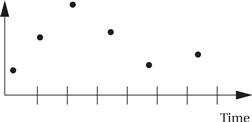
If the program ran fast enough to meet its deadline, the output would simply be a time-shifted copy of the input. But when the program runs over its allotted time, the output will become very different. Exactly what happens depends in part on the behavior of the A/D and D/A converters, so let’s make some assumptions. First, the A/D converter holds its current sample in a register until the next sample period, and the D/A converter changes its output whenever it receives a new sample. Next, a reasonable assumption about interrupt systems is that, when an interrupt is not satisfied and the device interrupts again, the device’s old value will disappear and be replaced by the new value. The basic situation that develops when the interrupt routine runs too long is something like this:
1. The A/D converter is prompted by the timer to generate a new value, saves it in the register, and requests an interrupt.
2. The interrupt handler runs too long from the last sample.
3. The A/D converter gets another sample at the next period.
4. The interrupt handler finishes its first request and then immediately responds to the second interrupt. It never sees the first sample and only gets the second one.
Thus, assuming that the interrupt handler takes 1.5 times longer than it should, here is how it would process the sample input:
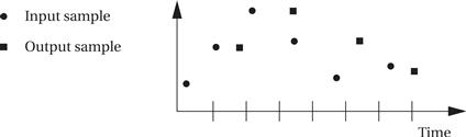
The output waveform is seriously distorted because the interrupt routine grabs the wrong samples and puts the results out at the wrong times.
The exact results of missing real-time deadlines depend on the detailed characteristics of the I/O devices and the nature of the timing violation. This makes debugging real-time problems especially difficult. Unfortunately, the best advice is that if a system exhibits truly unusual behavior, missed deadlines should be suspected. In-circuit emulators, logic analyzers, and even LEDs can be useful tools in checking the execution time of real-time code to determine whether it in fact meets its deadline.
4.6 Consumer Electronics Architecture
In this section we consider consumer electronics devices as an example of complex embedded systems and the platforms that support them.
4.6.1 Consumer Electronics use Cases and Requirements
Although some predict the complete convergence of all consumer electronic functions into a single device, much as has happened to the personal computer, we still have a variety of devices with different functions. However, consumer electronics devices have converged over the past decade around a set of common features that are supported by common architectural features. Not all devices have all features, depending on the way the device is to be used, but most devices select features from a common menu. Similarly, there is no single platform for consumer electronics devices, but the architectures in use are organized around some common themes.
This convergence is possible because these devices implement a few basic types of functions in various combinations: multimedia and communications. The style of multimedia or communications may vary, and different devices may use different formats, but this causes variations in hardware and software components within the basic architectural templates. In this section we will look at general features of consumer electronics devices; in the following sections we will study a few devices in more detail.
Functional requirements
Consumer electronics devices provide several types of services in different combinations:
• multimedia: The media may be audio, still images, or video (which includes both motion pictures and audio). These multimedia objects are generally stored in compressed form and must be uncompressed to be played (audio playback, video viewing, etc.). A large and growing number of standards have been developed for multimedia compression: MP3, Dolby DigitalTM, and so on for audio; JPEG for still images; MPEG-2, MPEG-4, H.264, and so on for video.
• data storage and management: Because people want to select what multimedia objects they save or play, data storage goes hand-in-hand with multimedia capture and display. Many devices provide PC-compatible file systems so that data can be shared more easily.
• communications: Communications may be relatively simple, such as a USB interface to a host computer. The communications link may also be more sophisticated, such as an Ethernet port or a cellular telephone link.
Nonfunctional requirements
Consumer electronics devices must meet several types of strict nonfunctional requirements as well. Many devices are battery-operated, which means that they must operate under strict energy budgets. A typical battery for a portable device provides only about 75 mW, which must support not only the processors and digital electronics but also the display, radio, and so on. Consumer electronics must also be very inexpensive. A typical primary processing chip must sell in the neighborhood of $10. These devices must also provide very high performance—sophisticated networking and multimedia compression require huge amounts of computation.
Use cases
Let’s consider some basic use cases of some basic operations. Figure 4.25 shows a use case for selecting and playing a multimedia object (an audio clip, a picture, etc.). Selecting an object makes use of both the user interface and the file system. Playing also makes use of the file system as well as the decoding subsystem and I/O subsystem.
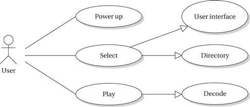
Figure 4.25 Use case for playing multimedia.
Figure 4.26 shows a use case for connecting to a client. The connection may be either over a local connection like USB or over the Internet. While some operations may be performed locally on the client device, most of the work is done on the host system while the connection is established.
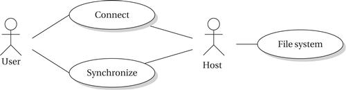
Figure 4.26 Use case of synchronizing with a host system.
Hardware architectures
Figure 4.27 shows a functional block diagram of a typical device. The storage system provides bulk, permanent storage. The network interface may provide a simple USB connection or a full-blown Internet connection.
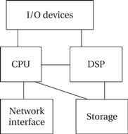
Figure 4.27 Hardware architecture of a generic consumer electronics device.
Multiprocessor architectures are common in many consumer multimedia devices. Figure 4.27 shows a two-processor architecture; if more computation is required, more DSPs and CPUs may be added. The RISC CPU runs the operating system, runs the user interface, maintains the file system, and so on. The DSP performs signal processing. The DSP may be programmable in some systems; in other cases, it may be one or more hardwired accelerators.
Operating systems
The operating system that runs on the CPU must maintain processes and the file system. Processes are necessary to provide concurrency—for example, the user wants to be able to push a button while the device is playing back audio. Depending on the complexity of the device, the operating system may not need to create tasks dynamically. If all tasks can be created using initialization code, the operating system can be made smaller and simpler.
4.6.2 File Systems
DOS file systems
DOS file allocation table (FAT) file systems refer to the file system developed by Microsoft for early versions of the DOS operating system [Mic00]. FAT can be implemented on flash storage devices as well as magnetic disks; wear-leveling algorithms for flash memory can be implemented without disturbing the basic operation of the file system. The aspects of the standards most relevant to camera operation are the format of directories and files on the storage medium. FAT can be implemented in a relatively small amount of code.
Flash memory
Many consumer electronics devices use flash memory for mass storage. Flash memory is a type of semiconductor memory that, unlike DRAM or SRAM, provides permanent storage. Values are stored in the flash memory cell as an electric charge using a specialized capacitor that can store the charge for years. The flash memory cell does not require an external power supply to maintain its value. Furthermore, the memory can be written electrically and, unlike previous generations of electrically-erasable semiconductor memory, can be written using standard power supply voltages and so does not need to be disconnected during programming.
Flash file systems
Flash memory has one important limitation that must be taken into account. Writing a flash memory cell causes mechanical stress that eventually wears out the cell. Today’s flash memories can reliably be written a million times but at some point will fail. While a million write cycles may sound like a lot, creating a single file may require many write operations, particularly to the part of the memory that stores the directory information.
A wear-leveling flash file system [Ban95] manages the use of flash memory locations to equalize wear while maintaining compatibility with existing file systems. A simple model of a standard file system has two layers: the bottom layer handles physical reads and writes on the storage device; the top layer provides a logical view of the file system A flash file system imposes an intermediate layer that allows the logical-to-physical mapping of files to be changed. This layer keeps track of how frequently different sections of the flash memory have been written and allocates data to equalize wear. It may also move the location of the directory structure while the file system is operating. Because the directory system receives the most wear, keeping it in one place may cause part of the memory to wear out before the rest, unnecessarily reducing the useful life of the memory device. Several flash file systems have been developed, such as Yet Another Flash Filing System (YAFFS) [Yaf11].
4.7 Platform-Level Performance Analysis
Bus-based systems add another layer of complication to performance analysis. Platform-level performance involves much more than the CPU. We often focus on the CPU because it processes instructions, but any part of the system can affect total system performance. More precisely, the CPU provides an upper bound on performance, but any other part of the system can slow down the CPU. Merely counting instruction execution times is not enough.
Consider the simple system of Figure 4.28. We want to move data from memory to the CPU to process it. To get the data from memory to the CPU we must:
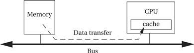
Figure 4.28 Platform-level data flows and performance.
The time required to transfer from the cache to the CPU is included in the instruction execution time, but the other two times are not.
Bandwidth as performance
The most basic measure of performance we are interested in is bandwidth—the rate at which we can move data. Ultimately, if we are interested in real-time performance, we are interested in real-time performance measured in seconds. But often the simplest way to measure performance is in units of clock cycles. However, different parts of the system will run at different clock rates. We have to make sure that we apply the right clock rate to each part of the performance estimate when we convert from clock cycles to seconds.
Bus bandwidth
Bandwidth questions often come up when we are transferring large blocks of data. For simplicity, let’s start by considering the bandwidth provided by only one system component, the bus. Consider an image of 320 # 240 pixels with each pixel composed of 3 bytes of data. This gives a grand total of 230,400 bytes of data. If these images are video frames, we want to check if we can push one frame through the system within the 1/30 sec that we have to process a frame before the next one arrives.
Let us assume that we can transfer one byte of data every microsecond, which implies a bus speed of 1 MHz. In this case, we would require 230,400 μs = 0.23 sec to transfer one frame. That is more than the 0.033 sec allotted to the data transfer. We would have to increase the transfer rate by 7# to satisfy our performance requirement.
We can increase bandwidth in two ways: we can increase the clock rate of the bus or we can increase the amount of data transferred per clock cycle. For example, if we increased the bus to carry four bytes or 32 bits per transfer, we would reduce the transfer time to 0.058 sec. If we could also increase the bus clock rate to 2 MHz, then we would reduce the transfer time to 0.029 sec, which is within our time budget for the transfer.
Bus bandwidth characteristics
How do we know how long it takes to transfer one unit of data? To determine that, we have to look at the data sheet for the bus. A bus transfer generally takes more than one clock cycle. Burst transfers, which move blocks of data to contiguous locations, may be more efficient per byte. We also need to know the width of the bus—how many bytes per transfer. Finally, we need to know the bus clock period, which in general will be different from the CPU clock period.
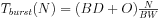
Bus bandwidth formulas
Let’s call the bus clock period P and the bus width W. We will put W in units of bytes but we could use other measures of width as well. We want to write formulas for the time required to transfer N bytes of data. We will write our basic formulas in units of bus cycles T, then convert those bus cycle counts to real time t using the bus clock period P:
 (Eq. 4.1)
As shown in Figure 4.29, a basic bus transfer transfers a W-wide set of bytes. The data transfer itself takes D clock cycles. (Ideally, D = 1, but a memory that introduces wait states is one example of a transfer that could require D > 1 cycles.) Addresses, handshaking, and other activities constitute overhead that may occur before (O1 ) or after (O2 ) the data. For simplicity, we will lump the overhead into O = O1 + O2 . This gives a total transfer time in clock cycles of:
 (Eq. 4.2)
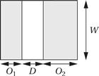
Figure 4.29 Times and data volumes in a basic bus transfer.
As shown in Figure 4.30, a burst transaction performs B transfers of W bytes each. Each of those transfers will require D clock cycles. The bus also introduces O cycles of overhead per burst. This gives
 (Eq. 4.3)
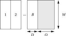
Figure 4.30 Times and data volumes in a burst bus transfer.
Component bandwidth
Bandwidth questions also come up in situations that we don’t normally think of as communications. Transferring data into and out of components also raises questions of bandwidth. The simplest illustration of this problem is memory.
The width of a memory determines the number of bits we can read from the memory in one cycle. That is a form of data bandwidth. We can change the types of memory components we use to change the memory bandwidth; we may also be able to change the format of our data to accommodate the memory components.
Memory aspect ratio
A single memory chip is not solely specified by the number of bits it can hold. As shown in Figure 4.31, memories of the same size can have different aspect ratios. For example, a 64-Mbit memory that is one bit wide will present 64 million addresses of one-bit data. The same size memory in a 4-bit-wide format will have 16 distinct addresses and an 8-bit-wide memory will have 8 million distinct addresses.
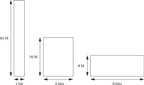
Figure 4.31 Memory aspect ratios.
Memory chips do not come in extremely wide aspect ratios but we can build wider memories by using several memories in parallel. By organizing memory chips into the proper aspect ratio for our application, we can build a memory system with the total amount of storage that we want and that presents the data width that we want.
The memory system width may also be determined by the memory modules we use. Rather than buy memory chips individually, we may buy memory as SIMMs or DIMMs. These memories are wide but generally only come in fairly standard widths.
Which aspect ratio is preferable for the overall memory system depends in part on the format of the data that we want to store in the memory and the speed with which it must be accessed, giving rise to bandwidth analysis.
Memory access times and bandwidth
We also have to consider the time required to read or write a memory. Once again, we refer to the component data sheets to find these values. Access times depend quite a bit on the type of memory chip used. Page modes operate similarly to burst modes in buses. If the memory is not synchronous, we can still refer the times between events back to the bus clock cycle to determine the number of clock cycles required for an access.
The basic form of the equation for memory transfer time is that of Eq. 4.3. where O is determined by the page mode overhead and D is the time between successive transfers.
However, the situation is slightly more complex if the data types don’t fit naturally into the width of the memory. Let’s say that we want to store color video pixels in our memory. A standard pixel is three 8-bit color values (red, green, blue, for example). A 24-bit-wide memory would allow us to read or write an entire pixel value in one access. An 8-bit-wide memory, in contrast, would require three accesses for the pixel. If we have a 32-bit-wide memory, we have two main choices: we could waste one byte of each transfer or use that byte to store unrelated data, or we could pack the pixels. In the latter case, the first read would get all of the first pixel and one byte of the second pixel; the second transfer would get the last two bytes of the second pixel and the first two bytes of the third pixel; and so forth. The total number of accesses required to read E data elements of w bits each out of a memory of width W is:
 (Eq. 4.4)
The next example applies our bandwidth models to a simple design problem.
Example 4.3 Performance Bottlenecks in a Bus-Based System
Consider a simple bus-based system:
We want to transfer data between the CPU and the memory over the bus. We need to be able to read a 320 # 240 video frame into the CPU at the rate of 30 frames/sec, for a total of 612,000 bytes/sec. Which will be the bottleneck and limit system performance: the bus or the memory?
Let’s assume that the bus has a 1-MHz clock rate (period of 10−6 sec) and is two bytes wide, with D = 1 and O = 3. This gives a total transfer time of
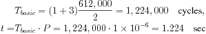
Because the total time to transfer one second’s worth of frames is more than one second, the bus is not fast enough for our application.
The memory provides a burst mode with B = 4 but is only 4 bits wide, giving W = 0.5. For this memory, D = 1 and O = 4. The clock period for this memory is 10−7 sec. Then
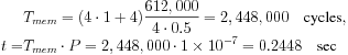
The memory requires less than one second to transfer the 30 frames that must be transmitted in one second, so it is fast enough.
One way to explore design trade-offs is to build a spreadsheet:
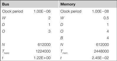
If we insert the formulas for bandwidth into the spreadsheet, we can change values like bus width and clock rate and instantly see their effects on available bandwidth.
4.8 Design Example: Alarm Clock
Our first system design example will be an alarm clock. We use a microprocessor to read the clock’s buttons and update the time display. Because we now have an understanding of I/O, we work through the steps of the methodology to go from a concept to a completed and tested system.
4.8.1 Requirements
The basic functions of an alarm clock are well understood and easy to enumerate. Figure 4.32 illustrates the front panel design for the alarm clock. The time is shown as four digits in 12-hour format; we use a light to distinguish between AM and PM. We use several buttons to set the clock time and alarm time. When we press the hour and minute buttons, we advance the hour and minute, respectively, by one. When setting the time, we must hold down the set time button while we hit the hour and minute buttons; the set alarm button works in a similar fashion. We turn the alarm on and off with the alarm on and alarm off buttons. When the alarm is activated, the alarm ready light is on. A separate speaker provides the audible alarm.
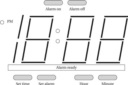
Figure 4.32 Front panel of the alarm clock.
We are now ready to create the requirements table:
| Name | Alarm clock |
| Purpose | A 24-hour digital clock with a single alarm. |
| Inputs | Six pushbuttons: set time, set alarm, hour, minute, alarm on, alarm off. |
| Outputs | Four-digit, clock-style output. PM indicator light. Alarm ready light. Buzzer. |
| Functions | Default mode: the display shows the current time. PM light is on from noon to midnight. Hour and minute buttons are used to advance time and alarm, respectively. Pressing one of these buttons increments the hour/minute once. Depress set time button: This button is held down while hour/minute buttons are pressed to set time. New time is automatically shown on display. Depress set alarm button: While this button is held down, display shifts to current alarm setting; depressing hour/minute buttons sets alarm value in a manner similar to setting time. Alarm on: puts clock in alarm-on state, causes clock to turn on buzzer when current time reaches alarm time, turns on alarm ready light. Alarm off: turns off buzzer, takes clock out of alarm-on state, turns off alarm ready light. |
| Performance | Displays hours and minutes but not seconds. Should be accurate within the accuracy of a typical microprocessor clock signal. (Excessive accuracy may unreasonably drive up the cost of generating an accurate clock.) |
| Manufacturing cost | Consumer product range. Cost will be dominated by the microprocessor system, not the buttons or display. |
| Power | Powered by AC through a standard power supply. |
| Physical size and weight | Small enough to fit on a nightstand with expected weight for an alarm clock. |
4.8.2 Specification
The basic function of the clock is simple, but we do need to create some classes and associated behaviors to clarify exactly how the user interface works.
Figure 4.33 shows the basic classes for the alarm clock. Borrowing a term from mechanical watches, we call the class that handles the basic clock operation the Mechanism class. We have three classes that represent physical elements: Lights* for all the digits and lights, Buttons* for all the buttons, and Speaker* for the sound output. The Buttons* class can easily be used directly by Mechanism. As discussed below, the physical display must be scanned to generate the digits output, so we introduce the Display class to abstract the physical lights.
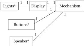
Figure 4.33 Class diagram for the alarm clock.
The details of the low-level user interface classes are shown in Figure 4.34. The Buzzer* class allows the buzzer to be turned on or off; we will use analog electronics to generate the buzz tone for the speaker. The Buttons* class provides read-only access to the current state of the buttons. The Lights* class allows us to drive the lights. However, to save pins on the display, Lights* provides signals for only one digit, along with a set of signals to indicate which digit is currently being addressed. We generate the display by scanning the digits periodically. That function is performed by the Display class, which makes the display appear as an unscanned, continuous display to the rest of the system.
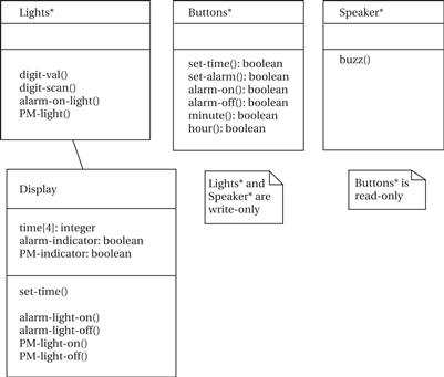
Figure 4.34 Details of user interface classes for the alarm clock.
The Mechanism class is described in Figure 4.35. This class keeps track of the current time, the current alarm time, whether the alarm has been turned on, and whether it is currently buzzing. The clock shows the time only to the minute, but it keeps internal time to the second. The time is kept as discrete digits rather than a single integer to simplify transferring the time to the display. The class provides two behaviors, both of which run continuously. First, scan-keyboard is responsible for looking at the inputs and updating the alarm and other functions as requested by the user. Second, update-time keeps the current time accurate.
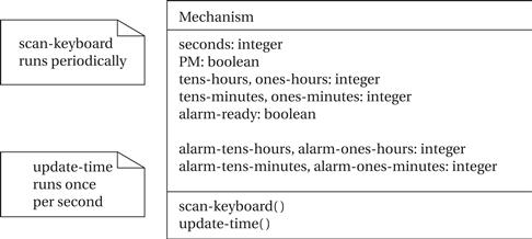
Figure 4.35 The Mechanism class.
Figure 4.36 shows the state diagram for update-time. This behavior is straightforward, but it must do several things. It is activated once per second and must update the seconds clock. If it has counted 60 seconds, it must then update the displayed time; when it does so, it must roll over between digits and keep track of AM-to-PM and PM-to-AM transitions. It sends the updated time to the display object. It also compares the time with the alarm setting and sets the alarm buzzing under the proper conditions.
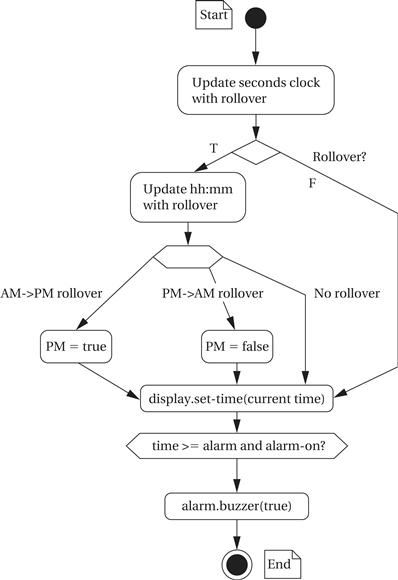
Figure 4.36 State diagram for update-time.
The state diagram for scan-keyboard is shown in Figure 4.37. This function is called periodically, frequently enough so that all the user’s button presses are caught by the system. Because the keyboard will be scanned several times per second, we don’t want to register the same button press several times. If, for example, we advanced the minutes count on every keyboard scan when the set-time and minutes buttons were pressed, the time would be advanced much too fast. To make the buttons respond more reasonably, the function computes button activations—it compares the current state of the button to the button’s value on the last scan, and it considers the button activated only when it is on for this scan but was off for the last scan. Once computing the activation values for all the buttons, it looks at the activation combinations and takes the appropriate actions. Before exiting, it saves the current button values for computing activations the next time this behavior is executed.
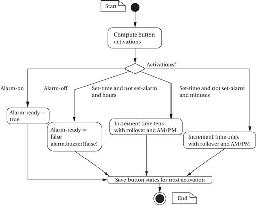
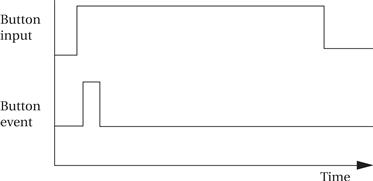
Figure 4.37 State diagram for scan-keyboard.
Figure 4.38 Preprocessing button inputs.
4.8.3 System Architecture
The software and hardware architectures of a system are always hard to completely separate, but let’s first consider the software architecture and then its implications on the hardware.
The system has both periodic and aperiodic components—the current time must obviously be updated periodically, and the button commands occur occasionally.
It seems reasonable to have the following two major software components:
• An interrupt-driven routine can update the current time. The current time will be kept in a variable in memory. A timer can be used to interrupt periodically and update the time. As seen in the subsequent discussion of the hardware architecture, the display must be sent the new value when the minute value changes. This routine can also maintain the PM indicator.
• A foreground program can poll the buttons and execute their commands. Because buttons are changed at a relatively slow rate, it makes no sense to add the hardware required to connect the buttons to interrupts. Instead, the foreground program will read the button values and then use simple conditional tests to implement the commands, including setting the current time, setting the alarm, and turning off the alarm. Another routine called by the foreground program will turn the buzzer on and off based on the alarm time.
An important question for the interrupt-driven current time handler is how often the timer interrupts occur. A one-minute interval would be very convenient for the software, but a one-minute timer would require a large number of counter bits. It is more realistic to use a one-second timer and to use a program variable to count the seconds in a minute.
The foreground code will be implemented as a while loop:
while (TRUE) {
read_buttons(button_values); /* read inputs */
process_command(button_values); /* do commands */
check_alarm(); /* decide whether to turn on the alarm */
}
The loop first reads the buttons using read_buttons(). In addition to reading the current button values from the input device, this routine must preprocess the button values so that the user interface code will respond properly. The buttons will remain depressed for many sample periods because the sample rate is much faster than any person can push and release buttons. We want to make sure that the clock responds to this as a single depression of the button, not one depression per sample interval. As shown in Figure 4.38, this can be done by performing a simple edge detection on the button input—the button event value is 1 for one sample period when the button is depressed and then goes back to 0 and does not return to 1 until the button is depressed and then released. This can be accomplished by a simple two-state machine.
The process_command() function is responsible for responding to button events. The check_alarm() function checks the current time against the alarm time and decides when to turn on the buzzer. This routine is kept separate from the command processing code because the alarm must go on when the proper time is reached, independent of the button inputs.
We have determined from the software architecture that we will need a timer connected to the CPU. We will also need logic to connect the buttons to the CPU bus. In addition to performing edge detection on the button inputs, we must also of course debounce the buttons.
The final step before starting to write code and build hardware is to draw the state transition graph for the clock’s commands. That diagram will be used to guide the implementation of the software components.
4.8.4 Component Design and Testing
The two major software components, the interrupt handler and the foreground code, can be implemented relatively straightforwardly. Because most of the functionality of the interrupt handler is in the interruption process itself, that code is best tested on the microprocessor platform. The foreground code can be more easily tested on the PC or workstation used for code development. We can create a testbench for this code that generates button depressions to exercise the state machine. We will also need to simulate the advancement of the system clock. Trying to directly execute the interrupt handler to control the clock is probably a bad idea—not only would that require some type of emulation of interrupts, but it would require us to count interrupts second by second. A better testing strategy is to add testing code that updates the clock, perhaps once per four iterations of the foreground while loop.
The timer will probably be a stock component, so we would then focus on implementing logic to interface to the buttons, display, and buzzer. The buttons will require debouncing logic. The display will require a register to hold the current display value in order to drive the display elements.
4.8.5 System Integration and Testing
Because this system has a small number of components, system integration is relatively easy. The software must be checked to ensure that debugging code has been turned off. Three types of tests can be performed. First, the clock’s accuracy can be checked against a reference clock. Second, the commands can be exercised from the buttons. Finally, the buzzer’s functionality should be verified.
4.9 Design Example: Audio Player
In this example we study the design of a portable MP3 player that decompresses music files as it plays.
4.9.1 Theory of Operation and Requirements
Audio players are often called MP3 players after the popular audio data format, although a number of audio compression formats have been developed and are in regular use. The earliest portable MP3 players were based on compact disc mechanisms. Modern MP3 players use either flash memory or disk drives to store music. An MP3 player performs three basic functions: audio storage, audio decompression, and user interface.
Audio decompression
Although audio compression is computationally intensive, audio decompression is relatively lightweight. The incoming bit stream has been encoded using a Huffman-style code, which must be decoded. The audio data itself is applied to a reconstruction filter, along with a few other parameters. MP3 decoding can, for example, be executed using only 10% of an ARM7 CPU.
Audio compression is a lossy process that relies on perceptual coding. The coder eliminates certain features of the audio stream so that the result can be encoded in fewer bits. It tries to eliminate features that are not easily perceived by the human audio system. Masking is one perceptual phenomenon that is exploited by perceptual coding. One tone can be masked by another if the tones are sufficiently close in frequency. Some audio features can also be masked if they occur too close in time after another feature.
The term MP3 comes from MPEG-1, layer 3; the MP3 spec is part of the MPEG-1 standard. That standard [Bra94] defined three layers of audio compression:
• Layer 1 (MP1) uses a lossless compression of subbands and an optional, simple masking model.
• Layer 2 (MP2) uses a more advanced masking model.
• Layer 3 (MP3) performs additional processing to provide lower bit rates.
The various layers support several different input sampling rates, output bit rates, and modes (mono, stereo, etc.).
We will concentrate on Layer 1, which illustrates the basic principles of MPEG audio coding. Figure 4.39 gives a block diagram of a Layer 1 encoder. The main processing path includes the filter bank and the quantizer/encoder. The filter bank splits the signal into a set of 32 subbands that are equally spaced in the frequency domain and together cover the entire frequency range of the audio. Audio signals tend to be more correlated within a narrower band, so splitting into subbands helps the encoder reduce the bit rate. The quantizer first scales each subband so that it fits within 6 bits of dynamic range, then quantizes based upon the current scale factor for that subband. The masking model selects the scale factors. It is driven by a separate fast Fourier transform (FFT); although in principle the filter bank could be used for masking, a separate FFT provides better results. The masking model chooses the scale factors for the subbands, which can change along with the audio stream. The MPEG standard does not dictate any particular masking model. The multiplexer at the output of the encoder passes along all the required data.
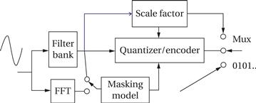
Figure 4.39 MPEG Layer 1 encoder.
MPEG data streams are divided into frames. A frame carries the basic MPEG data, error correction codes, and additional information. Figure 4.40 shows the format of an MPEG Layer 1 data frame.

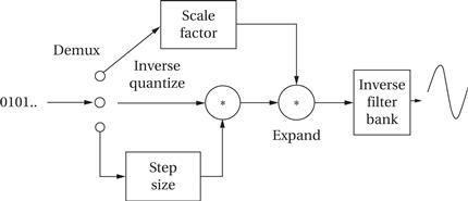
Figure 4.40 MPEG Layer 1 data frame format.
Figure 4.41 MPEG Layer 1 decoder.
MPEG audio decoding is a relatively straightforward process. A block diagram of an MPEG Layer 1 decoder is shown in Figure 4.41. After disassembling the data frame, the data are unscaled and inverse quantized to produce sample streams for the subband. An inverse filter bank then reassembles the subbands into the uncompressed signal.
User interface
The user interface of an MP3 player is usually kept simple to minimize both the physical size and power consumption of the device. Many players provide only a simple display and a few buttons.
File system
The file system of the player generally must be compatible with PCs. CD/MP3 players used compact discs that had been created on PCs. Today’s players can be plugged into USB ports and treated as disk drives on the host processor.
| Name | Audio player |
| Purpose | Play audio from files. |
| Inputs | Flash memory socket, on/off, play/stop, menu up/down. |
| Outputs | Speaker |
| Functions | Display list of files in flash memory, select file to play, play file. |
| Performance | Sufficient to play audio files at required rate. |
| Manufacturing cost | Approximately $25 |
| Power | 1 AAA battery |
| Physical size and weight | Approx. 1 in x 2 in, less than 2 oz |
The requirements table for the audio player are given in Figure 4.42. Although a commercial audio player would support at least MP3, a class project could be based on a player that used a simpler compression scheme. The specification could be extended to include USB for direct management of files on the device from a host system. These requirements state that the device should accept flash memory cards on which audio files have previously been loaded.
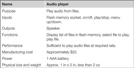
Figure 4.42 Requirements for the audio player.
4.9.2 Specification
Figure 4.43 shows the major classes in the audio player. The FileID class is an abstraction of a file in the flash file system. The controller class provides the method that operates the player.
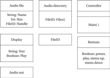
Figure 4.43 Classes in the audio player.
If file management is performed on a host device, then the basic operations to be specified are simple: file display/selection and playback.
Figure 4.44 shows a state diagram for file display/selection. This specification assumes that all files are in the root directory and that all files are playable audio.
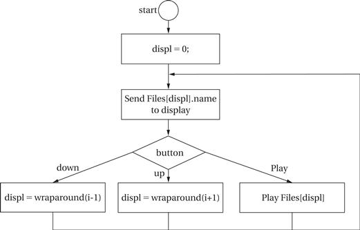
Figure 4.44 State diagram for file display and selection.
Figure 4.45 shows the state diagram for audio playback. The details of this operation depend on the format of the audio file. This state diagram refers to sending the samples to the audio system rather than explicitly sending them because playback and reading the next data frame must be overlapped to ensure continuous operation. The details of playback depend on the hardware platform selected, but will probably involve a DMA transfer.
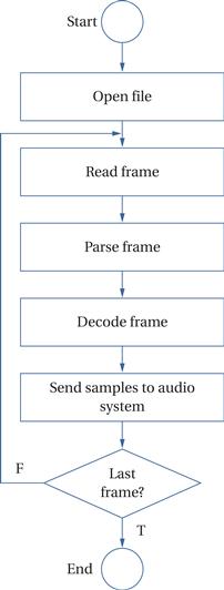
Figure 4.45 State diagram for audio playback.
4.9.3 System Architecture
Audio processors
The Cirrus CS7410 [Cir04B] is an audio controller designed for CD/MP3 players. The audio controller includes two processors. The 32-bit RISC processor is used to perform system control and audio decoding. The 16-bit DSP is used to perform audio effects such as equalization. The memory controller can be interfaced to several different types of memory: flash memory can be used for data or code storage; DRAM can be used as a buffer to handle temporary disruptions of the CD data stream. The audio interface unit puts out audio in formats that can be used by A/D converters. General-purpose I/O pins can be used to decode buttons, run displays, etc. Cirrus provides a reference design for a CD/MP3 player [Cir04A].
As shown in Figure 4.46, the Cirrus chip uses two processors, a RISC and a DSP. Given the low computational requirements of audio decompression, a single-processor platform would also be feasible.
The software architecture of this system is relatively simple. The only major complication occurs from the requirements for DMA or other method to overlap audio playback and file access.
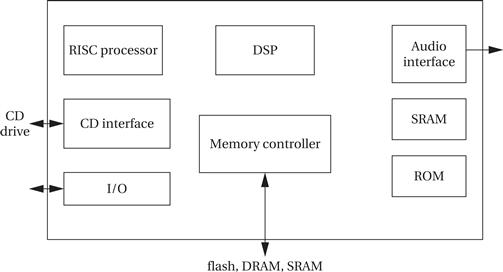
Figure 4.46 Architecture of a Cirrus audio processor for CD/MP3 players.
File systems
MP3 audio players originated a grassroots phenomenon. MP3 was designed to be used in conjunction with the MPEG-1 video compression standard. Home music collectors adopted MP3 files as a medium for storing compressed music. They passed around collections of MP3 files and playlists. These files were often shared as files written on CDs. Over time, consumer electronics manufacturers noticed the trend and made players for MP3 files. Because this approach was independently practiced by many different users, there are no standards for organizing MP3 files and playlists into directories. As a result, MP3 players must be able to navigate arbitrary user hierarchies, be able to find playlist files in any directory, etc. Manufacturers learned a lesson from this experience and defined file system organizations for other types of devices such as digital still cameras.
4.9.4 Component Design and Testing
The audio decompression object can be implemented from existing code or created as new software. In the case of an audio system that does not conform to a standard, it may be necessary to create an audio compression program to create test files.
The file system can either implement a known standard such as DOS FAT or can implement a new file system. While a nonstandard file system may be easier to implement on the device, it also requires software to create the file system.
The file system and user interface can be tested independently of the audio decompression system. The audio output system should be tested separately from the compression system. Testing of audio decompression requires sample audio files.
4.9.5 System Integration and Debugging
The most challenging part of system integration and debugging is ensuring that audio plays smoothly and without interruption. Any file access and audio output that operate concurrently should be separately tested, ideally using an easily recognizable test signal. Simple test signals such as tones will more readily show problems such as missed or delayed samples.
4.10 Summary
The microprocessor is only one component in an embedded computing system—memory and I/O devices are equally important. The microprocessor bus serves as the glue that binds all these components together. Hardware platforms for embedded systems are often built around common platforms with appropriate amounts of memory and I/O devices added on; low-level monitor software also plays an important role in these systems.
What we Learned
• CPU buses are built on handshaking protocols.
• A variety of memory components are available, which vary widely in speed, capacity, and other capabilities.
• An I/O device uses logic to interface to the bus so that the CPU can read and write the device’s registers.
• Embedded systems can be debugged using a variety of hardware and software methods.
• System-level performance depends not just on the CPU, but the memory and bus as well.
Further reading
Shanley and Anderson [Min95] describe the PCI bus in detail. Dahlin [Dah00] describes how to interface to a touchscreen. Collins [Col97] describes the design of microprocessor in-circuit emulators. Earnshaw et al. [Ear97] describe an advanced debugging environment for the ARM architecture.
Questions
Q4-1 Name three major components of a generic computing platform.
Q4-2 What role does the HAL play in the platform?
Q4-3 Draw UML state diagrams for device 1 and device 2 in a four-cycle handshake.
Q4-4 Describe the role of these signals in a bus:
Q4-5 Draw a UML sequence diagram that shows a four-cycle handshake between a bus master and a device.
Q4-6 Define these signal types in a timing diagram:
Q4-7 Draw a timing diagram with the following signals (where [t1,t2] is the time interval starting at t1 and ending at t2):
a. signal A is stable [0,10], changing [10,15], stable [15,30]
b. signal B is 1 [0,5], falling [5,7], 0 [7,20], changing [20,30]
c. signal C is changing [0,10], 0 [10,15], rising [15,18], 1 [18,25], changing [25,30]
Q4-8 Draw a timing diagram for a write operation with no wait states.
Q4-9 Draw a timing diagram for a read operation on a bus in which the read includes two wait states.
Q4-10 Draw a timing diagram for a write operation on a bus in which the write takes two wait states.
Q4-11 Draw a timing diagram for a burst write operation that writes four locations.
Q4-12 Draw a UML state diagram for a burst read operation with wait states. One state diagram is for the bus master and the other is for the device being read.
Q4-13 Draw a UML sequence diagram for a burst read operation with wait states.
Q4-14 Draw timing diagrams for
Q4-15 Draw a timing diagram that shows a complete DMA operation, including handing off the bus to the DMA controller, performing the DMA transfer, and returning bus control back to the CPU.
Q4-16 Draw UML state diagrams for a bus mastership transaction in which one side shows the CPU as the default bus master and the other shows the device that can request bus mastership.
Q4-17 Draw a UML sequence diagram for a bus mastership request, grant, and return.
Q4-18 Draw a UML sequence diagram that shows a DMA bus transaction and concurrent processing on the CPU.
Q4-19 Draw a UML sequence diagram for a complete DMA transaction, including the DMA controller requesting the bus, the DMA transaction itself, and returning control of the bus to the CPU.
Q4-20 Draw a UML sequence diagram showing a read operation across a bus bridge.
Q4-21 Draw a UML sequence diagram showing a write operation with wait states across a bus bridge.
Q4-22 Draw a UML sequence diagram for a read transaction that includes a DRAM refresh operation. The sequence diagram should include the CPU, the DRAM interface, and the DRAM internals to show the refresh itself.
Q4-23 Draw a UML sequence diagram for an SDRAM read operation. Show the activity of each of the SDRAM signals.
Q4-24 What is the role of a memory controller in a computing platform?
Q4-25 What hardware factors might be considered when choosing a computing platform?
Q4-26 What software factors might be considered when choosing a computing platform?
Q4-27 Write ARM assembly language code that handles a breakpoint. It should save the necessary registers, call a subroutine to communicate with the host, and upon return from the host, cause the breakpointed instruction to be properly executed.
Q4-28 Assume an A/D converter is supplying samples at 44.1 kHz.
a. How much time is available per sample for CPU operations?
b. If the interrupt handler executes 100 instructions obtaining the sample and passing it onto the application routine, how many instructions can be executed on a 20-MHz RISC processor that executes 1 instruction per cycle?
Q4-29 If an interrupt handler executes for too long and the next interrupt occurs before the last call to the handler has finished, what happens?
Q4-30 Consider a system in which an interrupt handler passes on samples to an FIR filter program that runs in the background.
a. If the interrupt handler takes too long, how does the FIR filter’s output change?
b. If the FIR filter code takes too long, how does its output change?
Q4-31 Assume that your microprocessor implements an ICE instruction that asserts a bus signal that causes a microprocessor in-circuit emulator to start. Also assume that the microprocessor allows all internal registers to be observed and controlled through a boundary scan chain. Draw a UML sequence diagram of the ICE operation, including execution of the ICE instruction, uploading the microprocessor state to the ICE, and returning control to the microprocessor’s program. The sequence diagram should include the microprocessor, the microprocessor in-circuit emulator, and the user.
Q4-32 Why might an embedded computing system want to implement a DOS-compatible file system?
Q4-33 Name two example embedded systems that implement a DOS-compatible file system.
Q4-34 We are given a 1-word-wide bus that supports single-word and burst transfers. The overhead of the single-word or dual-word transfer is 2 clock cycles (O = 2). Plot the breakeven point between single-word and burst transfers for several values of burst overhead—for each value of overhead, plot the length of burst transfer at which the burst-transfer is as fast as a series of single-word transfers. Plot breakeven for burst overhead values of 0, 1, 2, and 3 cycles.
Q4-35 We are given a 2-word-wide bus that supports single-word, dual-word (same clock cycle) and burst transfers. The overhead of the single-word or dual-word transfer is 2 clock cycles (O = 2) and a data transfer takes one clock cycle per single or dual word (D = 1). Plot the breakeven point between dual-word and burst transfers for several values of burst overhead—for each value of overhead, plot the length of burst transfer at which the burst-transfer is as fast as a series of single-word transfers. Plot breakeven for burst overhead values of 1, 2, and 3 cycles.
Q4-36 We are given a 2-byte-wide bus that supports single-byte, dual-word (same clock cycle) and burst transfers. The overhead of the single-byte or dual-byte transfer is 1 clock cycle. You want to send a 1080P video frame at a resolution of 1920 # 1080 pixels with three bytes per pixel. Compare the difference in bus transfer times if the pixels are packed vs. sending a pixel as a 2-byte followed by a single-byte transfer.
Q4-37 Determine the design parameters for an audio system:
a. Determine the total bytes/sec required for an audio signal of 16 bits/sample per channel, two channels, sampled at 44.1 kHz.
b. Given a clock period P = 20 MHz for a bus, determine the bus width required assuming that nonburst mode transfers are used and D = O = 1.
c. Given a clock period P = 20 MHz for a bus, determine the bus width required assuming burst transfers of length four and D = O = 1.
d. Assume the data signal now contains both the original audio signal and a compressed version of the audio at a bit rate of 1/10 the input audio signal. Compute the total data bandwidth and the bus bandwidth for burst transfers of length four with P = 20 MHz and D = O = 1.
Q4-38 You are designing a system a bus-based computer: the input device I1 sends its data to program P1; P1 sends its output to output device O1. Is there any way to overlap bus transfers and computations in this system?
Lab exercises
L4-1 Use a logic analyzer to view system activity on your bus.
L4-2 If your logic analyzer is capable of on-the-fly disassembly, use it to display bus activity in the form of instructions, rather than simply 1s and 0s.
L4-3 Attach LEDs to your system bus so that you can monitor its activity. For example, use an LED to monitor the read/write line on the bus.
L4-4 Design logic to interface an I/O device to your microprocessor.
L4-5 Use a data dump program to study the format of data on a flash memory card used as a file system.
L4-6 Have someone else deliberately introduce a bug into one of your programs, and then use the appropriate debugging tools to find and correct the bug.
L4-7 Identify the different bus transaction types in your platform. Compute the best-case bus bandwidth.
L4-8 Construct a simple program to access memory in widely separated places. Measure the memory system bandwidth and compare to the best-case bandwidth.
L4-9 Construct a simple program to perform some memory accesses. Use a logic analyzer to study the bus activity. Determine what types of bus modes are used for the transfers.