The I2C bus consists of two wires, one data (SDA), and one clock (SCL). Both are passively pulled to VCC (on the Raspberry Pi, this is 3.3 V) with pull-up resistors. The Raspberry Pi will control the clock by pulling it low every cycle and the data line can be pulled low by Raspberry Pi to send commands or by the connected device to respond with data:
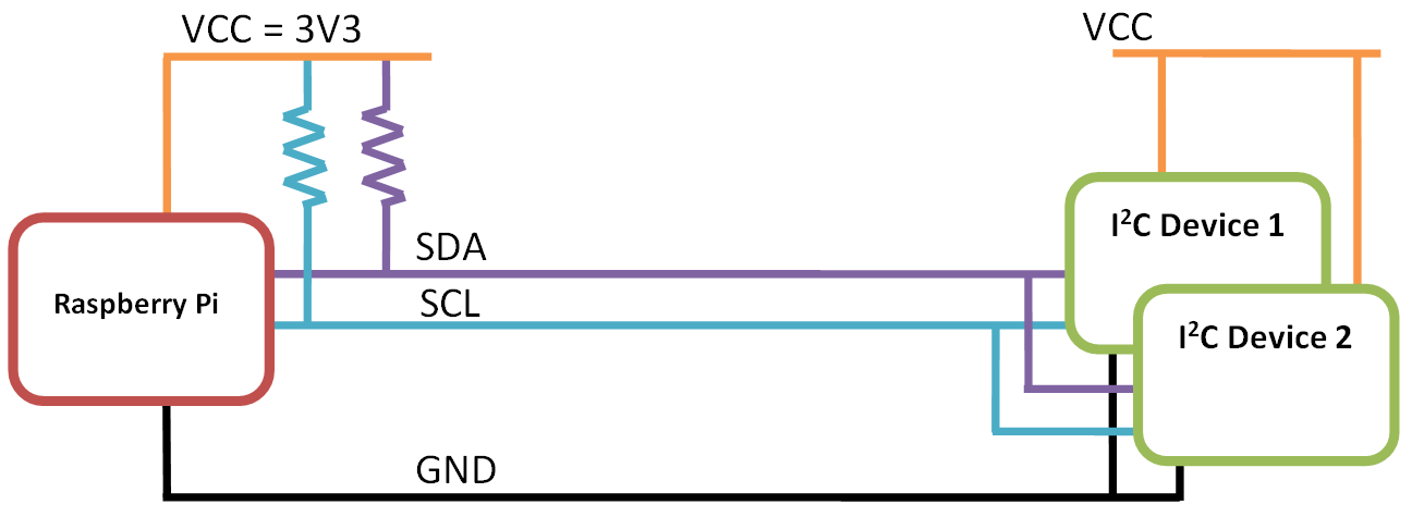
Since the slave devices can only pull the data line to GND, the device may be powered by 3.3 V or even 5 V without the risk of driving the GPIO pins too high (remember that the Raspberry Pi GPIO is not able to handle voltages over 3.3 V). This should work as long as the I2C bus of the device can recognize the logic maximum a 3.3 V rather than 5 V. The I2C device must not have its own pull-up resistors fitted, as this will cause the GPIO pins to be pulled to the supply voltage of the I2C device.
Note that the PCF8591 module used in this chapter has resistors fitted; therefore, we must only use VCC = 3V3. A bidirectional logic level converter can be used to overcome any issues with logic levels. One such device is the Adafruit I2C bidirectional logic level translator module, which is shown in the following image:

In addition to ensuring that any logic voltages are at suitable levels for the device you are using, it will allow the bus to be extended over longer wires (the level shifter will also act as a bus repeater).