ELECTRONIC
CONSTRUCTION
TECHNIQUES
CONSTRUCTION
TECHNIQUES
To operate all but the simplest robots requires an electronic circuit of one type or another. The way you construct these circuits will largely determine how well your robot functions and how long it will last. Poor performance and limited life inevitably result when hobbyists use so-called rat’s nest construction techniques such as soldering together the loose leads of components.
Using proper construction techniques will ensure that your robot circuits work well and last as long as you have a use for them. This chapter covers the basics of several types of construction techniques, starting with the basics of soldering, wire-wrapping, and some circuit prototyping techniques. While only the fundamentals are being presented, these methods, techniques, and tools are useful for even very sophisticated circuitry. For more details, consult a book on electronic construction techniques. Appendix A contains a list of suggested sources.
Soldering is the process of heating up two pieces of metal together and electrically joining them using a (relatively) low melting temperature metal (normally a lead-tin alloy). Discrete components, chips, printed circuit boards, and wires can all be joined by soldering them together. Soldering is not a construction technique and will not provide a robust mechanical connection that can be used in robot structures. Soldering sounds and looks simple enough, but there is a lot of science behind it and care must be taken to get strong, reliable connections (called joints) without damaging any of the components being soldered.
Fig. 7-1 shows the important aspects of a solder joint. The two pieces of metal to be connected (which is almost always copper) are joined by another metal (the solder) melted to them. When the solder is melted to the copper, it should wet smoothly over the entire copper surface. Even though the solder melts at a lower temperature than the copper, there are very thin interfaces produced that consist of a copper/solder alloy. These interfaces are called the intermetallic regions of the solder joints and one of the goals of soldering is to make sure these regions are as thin as possible to avoid alloying of the copper and solder (which raises the melting point of the solder and makes the joint brittle).

The following sections provide an overview of soldering. If you solder sporadically with months in between turning on your soldering iron, it is a good idea to review this material to ensure that the work is carried out efficiently and safely.
Keep the following points in mind when soldering:
- Keep your fingers away from the tip of the soldering pencil. A hot soldering iron can seriously burn you.
- Never touch a solder joint until after it has cooled.
- While using the soldering iron, always place it in a properly designed iron stand.
- To avoid inhaling the fumes for any length of time, work only in a well-ventilated area. While the fumes produced during soldering are not particularly offensive, they can be surprisingly toxic.
- Always wear eye protection such as safety glasses or optically clear goggles when clipping leads.
- Keep a fire extinguisher handy, just in case.
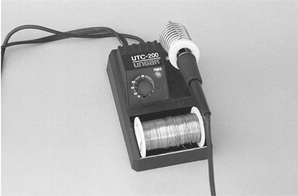
7.1.2.1 Soldering iron and tip When you are looking for a soldering iron, choose
one that is designed for electronics, like the one in Fig. 7-2. The iron should have a fairly
low wattage rating (not higher than 30 W). Most soldering irons or pencils are designed
so you can change the tips as easily as changing a lightbulb. Make sure that you have the
smallest pointed tip available for your iron as it will be required for small electronics
assembly. It is a good idea to buy a soldering iron that is grounded to keep from running
the risk of damaging sensitive electronic components by subjecting them to electrostatic
discharge.
Do not use the instant-on type soldering guns favored in the old tube days, and definitely
do not use an iron that was designed for plumbing. These types of irons produce far too
much unregulated heat and can easily damage the components being soldered.
If your soldering iron has a temperature control and readout, dial it to between 665 and
680°F. This is the typical melting point for solder and will pose the minimum danger of
damage to the electronic components. If your iron has just the control and lacks a heat
readout, set it to low initially. Wait a few minutes for the iron to heat up, then try one or
two test connections. Adjust the heat control so that solder flows onto the connection in
under 5 s.
Remember that when you are not using your soldering iron, keep it in an insulated
stand.
Which soldering tip you choose is important. For best results, use a fine tip designed
specifically for printed circuit board use (unless you are soldering larger wires; in that case,
use a larger tip). Tips are made to fit certain types and brands of soldering irons, so make
sure you get ones that are made for your iron.
7.1.2.2 Sponge Keep a damp sponge (just about any type of kitchen sponge will do)
by the soldering station and use it to wipe off extra solder. Do not allow globs of solder to
remain on the tip. The glob may come off while you’re soldering and ruin the connection.
The excess solder can also draw away heat from the tip of the pencil, causing a poor soldering
job. You’ll have to rewet the sponge now and then if you are doing lots of soldering.
Never wipe solder off onto a dry sponge, as the sponge could melt or catch on fire.
7.1.2.3 Solder and flux You should use only 63% lead/37% tin rosin core solder.
It comes in different thicknesses; for best results, use the thin type (0.050 in) for most electronics
work, especially if you’re working with printed circuit boards. Never use acid core or
silver solder on electronic equipment. (Note: certain silver-bearing solders are available for
specialty electronics work, and they are acceptable to use although a lot more expensive
than tin–lead solders.)
You have probably heard about lead-free solders, which, not surprisingly, do not contain
any lead in an effort to protect the environment. Unless you are well versed in soldering and
are certain that all the components that are going to be soldered have had their leads prepared
for lead-free solders, then it is highly recommended that you stay away from them.
Lead-free solders melt at a higher temperature than tin–lead solders and lead contamination
can cause even higher temperature melting points, which will make it very difficult to
remove the components.
Flux is a weak heat-activated acid that cleans the metal surfaces of the components being
soldered of oxides and some contaminants. In some cases, such as soldering large wires, you
may find it advantageous to apply liquid flux to the surfaces to ensure the larger areas are
cleaned during the solder process. To avoid getting into trouble with liquid flux, only buy flux
at the store where you bought your solder and make sure that it is the same formulation as
the flux in the solder. There are very aggressive fluxes designed for specialized applications
that will literally dissolve your components and solder iron tip. If you aren’t sure, then refrain
from buying any flux and rub the connections with steel wool before soldering to clean off
the surfaces to be soldered.
Solder should be kept clean and dry. Avoid tossing your spool of solder into your electronics
junk bin. It can collect dust, grime, oil, grease, and other contaminants. Dirty solder
requires more heat to melt. In addition, the grime fuses with the solder and melds into the
connection. If your solder becomes dirty, wipe it off with a damp paper towel soaked in
alcohol, and let it dry.
7.1.2.4 Soldering tools Basic soldering tools include a good pair of small needle-nose
pliers, wire strippers, and wire cutters (sometimes called side or diagonal cutters). The
stripper should have a dial that lets you select the gauge of wire you are using. A pair of
nippy cutters, which cuts wire leads flush to the surface of the board, is also handy.
A heat sink should be avoided during soldering—some people may say that it is necessary
to avoid heat damage to components, but a heat sink will raise the length of time the iron will have to be applied to the joint in order to melt the solder and could result in poor solder joints as well as an increased amount of heat being passed to the component. As discussed in the following, the iron should only be in contact with the component’s leads for a
few seconds, much less than the amount of time required to damage the component.
7.1.2.5 Cleaning supplies It is often necessary to clean up before and after you solder. Isopropyl alcohol makes a good, all-around cleaner to remove flux after soldering. After
the board has cooled, flux can form a hard surface that is difficult to remove. The best way
to clean a circuit board is to use isopropyl alcohol in an ultrasonic cleaner, but you can also
use a denture brush (which has much stiffer bristles than an ordinary toothbrush) with isopropyl
alcohol as well.
7.1.2.6 Solder vacuum and solder braid These tools are used for removing
excess solder and removing components after they have been soldered. Desoldering (removing
components that have been soldered to a board) is a tricky process that even with a lot
of skill can result in a damaged circuit board and components. To minimize the need for desoldering,
you should take care to ensure the correct components are being soldered in the
correct orientation and use sockets instead of soldering wherever possible.
The basis of successful soldering is to use the soldering iron to heat up the work, whether it
is a component lead, a wire, or whatever. You then apply the solder to the work. If the solder
doesn’t flow onto the joint, then check the iron’s temperature, add a bit more rosin core
solder or even add a bit of liquid flux. Once the solder flows around the joint (and some will
flow to the tip), remove the iron and let the joint cool. The joint should look smooth and
shiny. If the solder appears dull and crinkly, then you have a cold joint. To fix the joint,
apply the soldering iron again to remelt the solder.
Avoid disturbing the solder as it cools; a cold joint might be the result. Do not apply heat
any longer than necessary. Prolonged heat can permanently ruin electronic components. A
good rule of thumb is that if the iron is on any one spot for more than 5 s, it’s too long. If
at all possible, you should keep the iron at a 30° to 40° angle for best results. Most tips are
beveled for this purpose.
Apply only as much solder to the joint as is required to coat the lead and circuit board
pad. A heavy-handed soldering job may lead to soldering bridges, which is when one joint
melds with joints around it. At best, solder bridges cause the circuit to cease working; at
worst, they cause short circuits that can burn out the entire board.
When soldering on printed circuit boards, you’ll need to clip off the excess leads that protrude
beyond the solder joint. Use a pair of diagonal or nippy cutters for this task. Be sure
to protect your eyes when cutting the lead.
After soldering, wipe the hot tip on the solder sponge to remove any excess solder, flux, and
contaminants. Then let the iron cool. After many hours of use, the soldering tip will become
old, pitted, and deformed. This is a good time to replace the tip. Old or damaged tips impair the transfer of heat from the iron to the connection, which can lead to poor soldering joints. Be sure to replace the tip with one made specifically for your soldering iron. Tips are generally not interchangeable between brands.
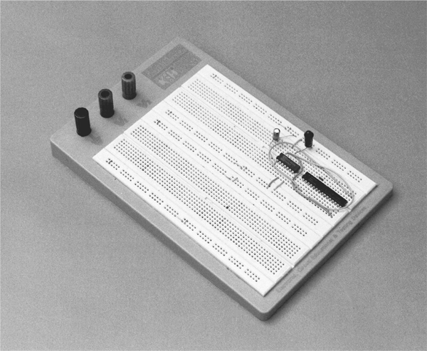
The term breadboard is used for a variety of experimenter wired circuit products. In this
book, the term will be used to describe the temporary prototyping circuit platform shown
in Fig. 7-3. in which the holes are connected to adjacent ones by a spring-loaded connector.
The typical arrangement is to have the interior holes connected outward while the outside
rows of holes are connected together to provide a bus structure for power and common signals.
Wire (typically 22 gauge) and most electronic components can be pushed into the circuit
to make connections and, when the application is finished, to pull out for reuse.

Breadboards are engineered to enable you to experiment with a circuit, without the trouble
of soldering. When you are assured that the circuit works, you may use one of the other
four construction techniques described in this chapter to make the design permanent. A
typical solderless breadboard mounted on a metal carrier is shown in Fig. 7-4. Breadboards
are available in many different sizes and styles, but most provide rows of common tie points
that are suitable for testing ICs, resistors, capacitors, and most other components that have
standard lead diameters.
It is a good idea to first test all the circuits you build on a solderless breadboard. It is
important to note that the resistance between adjacent pins is on the order of 5 Ω and the
capacitance between connectors can be as high as 2 pF. These parasitic impedances
mean that your circuit may not perform properly in all cases (especially for currents over
100 mA or signals switching at a few MHz) and you may have to resort to one of the
other prototyping methodologies described in the following. It should also be noted that
breadboard component connections can come loose when under vibration—such as in a mobile robot.
There are many different commercial products that allow you to solder together a custom
circuit reasonably quickly and easily. These products may have generic names like breadboard
circuit boards, universal solder boards, or experimenters’ PC boards. The Vector line
of products is commonly used by many robot experimenters. These boards consist of a
series of copper strips (which can be cut) to allow you to create custom circuits surprisingly
easily using standard PCB soldering techniques. Other prototyping PCBs have sockets and
commonly used circuits already etched into the PCBs to further simplify the assembly and
wiring of the circuit.
The main disadvantage of universal solder boards is that they don’t provide for extremely
efficient use of space. It can be difficult to cram the components onto a small space on the
board, and you will find that it takes some experience to properly plan your circuits. For this
reason, only use prototyping PCBs when wiring a fairly small and simple circuit. Remember
to drill mounting holes to secure the board in whatever enclosure or structure you are using.
Point-to-point wiring refers to the practice of mounting electronic components to a prototyping
PCB and connecting the leads together directly with solder. This technique was used
extensively in the pre-IC days and was often found on commercial products. An example of
a circuit built on a prototyping PCB and connected together using point-to-point wiring is
shown in Fig. 7-5.

When building point-to-point wired circuits, you must be careful to use insulated wire as
point-to-point construction invites short circuits and burnouts. Point-to-point wiring is the
most difficult method of creating circuitry discussed in this chapter, but often it is the only
method that allows you to get a robust circuit built quickly. Remember to start small and
don’t be afraid to experiment with different techniques in order to get the most efficient
circuitry.
An older method used to wire complex circuitry together is known as wire-wrapping: a
bared wire is literally wrapped around a long post, which is connected to the pin of an IC
or some other component. Wire-wrapping can be used to create very complex circuits, and
it is surprisingly robust. However, there are a number of downsides to this wiring method
that you should be aware of.
Wire-wrapping requires specialized tools, component sockets (with long, square leads),
and prototyping PCBs—each of which can be substantially more expensive than standard
parts. It also takes a surprisingly long time. Professional wire-wrappers with automated
equipment plan on each wire connection taking 30 s; starting out with hobbyist tools you
will be hard pressed to perform (on average) one wire every 3 minutes. It should also be
noted that a complex wire-wrapped board quickly becomes a rat’s nest and wiring errors are
extremely difficult to find. Finally, wiring power and analog components into a wire-wrapped
circuit is difficult and can be extremely time consuming.
Probably the most efficient method of prototyping circuits is to design a simple printed circuit
board and have a small number of samples built by a quick turn manufacturer. Depending
on your location, you could conceivably have your PCBs within a business day. Quick
turn PCBs (like the one shown in Fig. 7-6) are also surprisingly cost efficient—you should
plan on the PCBs costing $5 per square inch, approximately the same as what you would
pay for PCBs, sockets, and wiring for a wire-wrapped circuit. For a beginner, the time spent
designing the PCB is similar to that of wire-wrapping a PCB.

The big advantage of using quick turn PCBs is the ability to change and replicate the circuit
very quickly. Using any of the other prototyping techniques previously discussed, the
effort in wiring is only applied to one circuit; the time increases linearly with each additional
circuit built. A PCB design can be replicated without any additional investment in time and
certainly adds to the professionalism of a robot.
An understandable concern about designing printed circuit boards is the time required to
learn how to use the design tools, their cost, and learning how to efficiently lay out circuits
on a PCB. Currently there are a number of open source software projects and commercial
products that allow hobbyists to design PCBs and produce Gerber files (which are the
design files used to manufacture the PCBs) for free. There are quite a few books devoted to
explaining how PCB layout is accomplished and lists many of the tricks that you should be
aware of. Learning how to design PCBs is a marketable skill and one that will certainly pay
off in the future.
Robots are often constructed from subsystems that may not be located on the same circuit
board. You must therefore know how to connect subsystems on different circuit
boards. Avoid the temptation to directly solder wires between boards. This makes it much
harder to work with your robot, including testing variations of your designs with different
subsystems.
Instead, use connectors whenever possible, as shown in Fig. 7-7. In this approach you
connect the various subsystems of your robot using short lengths of wire. You terminate
each wire with a connector of some type or another. The connectors attach to mating pins
on each circuit board.
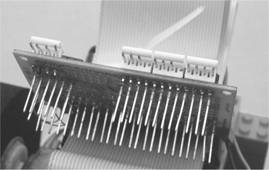
You don’t need fancy cables and cable connectors for your robots. In fact, these can add
significant weight to your ’bot. Instead, use ordinary 20- to 26-gauge wire, terminated with
single- or double-row plastic connectors. You can use ribbon cable for the wire or individual
insulated strips of wire. Use plastic ties to bundle the wires together. The plastic connectors
are made to mate with single- and double-row headers soldered directly on the circuit board.
You can buy connectors and headers that have different numbers of pins or you can salvage
them from old parts (the typical VCR is chock-full of them!).
When making interconnecting cables, cut the wires to length so there is a modest amount
of slack between subsystems. You don’t want, or need, gobs of excess wire. Nor do you want
the wire lengths so short that the components are put under stress when you connect them
together.
The ancient Egyptians discovered static electricity when they rubbed animal fur against the
smooth surface of amber. Once the materials were rubbed together, they tended to cling to
one another. Similarly, two pieces of fur that were rubbed against the amber tended to separate
when they were drawn together. While the Egyptians didn’t understand this mysterious
unseen force—better known now as static electricity—they knew it existed.
Today, you can encounter static electricity by doing nothing more than walking across a
carpeted floor. As you walk, your feet rub against the carpet, and your body takes on a
static charge. Touch a metal object, like a doorknob or a metal sink, and that static is quickly
discharged from your body. You feel the discharge as a shock.
Carpet shock has never been known to kill anyone. The amount of voltage and current
is far too low to cause great bodily harm. But the same isn’t true of electronic circuits. Considering
how your body can develop a 10,000- to 50,000-V charge when you walk across
a carpet, try to imagine what that might do to electrical components rated at just 5 or 15 V.
The sudden crash of electrical energy can burn holes right through a sensitive transistor or
integrated circuit, rendering it completely useless.
Transistors and integrated circuits designed around a metal-oxide substrate can be particularly
sensitive to high voltages, regardless of the current level. These components include
MOSFET transistors, CMOS integrated circuits, and most computer microprocessors.
Plastic is one of the greatest sources of static electricity. Storage and shipping containers
are often made of plastic, and it’s a great temptation to dump your static-sensitive devices
into these containers. Don’t do it. Invariably, static electricity will develop, and the component
could be damaged. Unfortunately, there’s no way to tell if a static-sensitive part has
become damaged by electrostatic discharge just by looking at it, so you won’t know things
are amiss until you actually try to use the component. At first, you’ll think the circuit has
gone haywire or that your wiring is at fault. If you’re like most, you won’t blame the transistors
and ICs until well after you’ve torn the rest of the circuit apart.
It’s best to store static-sensitive components using one of the following methods. All
work by grounding the leads of the IC or transistor together, which diminishes the effect of
a strong jolt of static electricity. Note that none of these storage methods is 100 percent
foolproof.
- Anti-static mat. This mat looks like a black sponge, but it’s really conductive foam. You can (and should) test this by placing the leads of a volt-ohm meter on either side of a length of the foam. Dial the meter to ohms. You should get a reading instead of an open circuit. The foam can easily be reused, and large sheets make convenient storage pads for many components.
- Anti-static pouch or bag. Anti-static pouches are made of a special plastic (which generates little static) and are coated on the inside with a conductive layer. The bags are available in a variety of forms. Many are a smoky black or gray; others are pink or jet black. As with mats, you should never assume a storage pouch is anti-static just from its color. Check the coating on the inside with a volt-ohm meter—its resistance should be in the 10k to 1 MΩ range.
- Anti-static tube. The vast majority of chips are shipped and stored in convenient plastic tubes. These tubes help protect the leads of the IC and are well suited to automatic manufacturing techniques. The construction of the tube is similar to the anti-static pouch: plastic on the outside, a thin layer of conductive material on the inside. You can often get tubes from electronic supply stores by just asking for leftover tubes that would normally be thrown away. It is a good idea to only put one type of chip in each tube, label the tube, and keep the same family of chips together. This will make finding specific components much easier.
Consider using any and all of the following simple techniques to reduce and eliminate the
risk of electrostatic discharge.
- Wear low-static clothing and shoes. Your choice of clothing can affect the amount of static buildup in your body. Whenever possible, wear natural fabrics such as cotton or wool. Avoid wearing polyester and acetate clothing, as these tend to develop large amounts of static.
- Use an anti-static wrist strap. The wrist strap grounds you at all times and prevents static buildup. The strap is one of the most effective means for eliminating electrostatic discharge, and it’s one of the least expensive.
- Ground your soldering iron. If your soldering pencil operates from AC current, it should be grounded. A grounded iron not only helps prevent damage from electrostatic discharge; it also lessens the chance of receiving a bad shock should you accidentally touch a live wire.
- Use component sockets. When you build projects that use ICs, install sockets first. When the entire circuit has been completely wired, you can check your work, then add the chips. Note that some sockets are polarized so the component will fit into them one way only. Be sure to observe this polarity when wiring the socket.
While building circuits for your robots, observe the good design principles described in the
following sections, even if the schematic diagrams you are working from don’t include them.
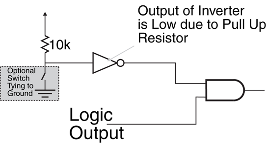
When a digital electronic chip input is left unconnected or floating, the value presented at
the input is indeterminate. This is especially true for CMOS chips, which use the gates of
MOSFET chips as inputs (TTL inputs are automatically high when inputs are left floating).
To ensure that the inputs values are a known value, a pull up should be used or, if the input
must be low during operation, then an inverted pull up (shown in Fig. 7-8) should be used.
Pull-down resistors on logic inputs should be avoided because of the low resistance (less
than 150 Ω) required to ensure TTL inputs are at a low value. To raise the input to a high
value, a high-current source must be applied to the input pin to overcome the pull-down
resistor. The pull-up resistor can be a relatively high value (10k or more) to minimize any
possible power drain and allow simple changes to logic without large current flows.
Some electronic components, especially fast-acting logic chips, generate a lot of noise in
the power supply lines. You can reduce or eliminate this noise by putting bypass (so-called
decoupling) capacitors between the +V and ground rails of all chips as close to the power
supply pins as possible, as shown in Fig. 7-9. Suggested values are 0.01 μF to 0.1 μF. If
you are using polarized parts, be sure to properly orient the capacitor.

Long leads on components can introduce noise in other parts of a circuit. The long leads
also act as a virtual antenna, picking up stray signals from the circuit, from overhead lighting, and even from your own body. When designing and building circuits, strive for the
shortest lead lengths on all components. This means soldering the components close to the
board and clipping off any excess lead length, and if you are breaking any connections cut
the wires or PCB traces as close to the chip pin as possible.
A ground loop is when the ground wire of a circuit comes back and meets itself. The +V and
ground of your circuits should always have dead ends to them. Ground loops can cause
erratic behavior due to excessive noise in the circuit, which can be very difficult to track
down to a root cause.
To learn more about . . . |
Read |
|
Tools for circuit construction |
Chapter 6, “Tools” |
|
Where to find electronic components |
Chapter 4, “Buying Parts” |
|
Where to find mechanical parts |
Chapter 4, “Buying Parts” |
|
Understanding components used in electronic circuitry |
Chapter 5, “Electronic Components” |