1.1 Historical Perspective
1.1.1 Rise of the Semiconductor Industry

This publicity photo accurately depicts the working relationship that led to the invention of the transistor at BTL: Brattain handles the apparatus, Bardeen enters data, and Shockley looks on.
Courtesy AIP Emilio Segrè Visual Archives, Brattain Collection
Silicon has much larger bandgap energy than germanium (1.124 vs. 0.664 eV), which means orders-of-magnitude smaller reverse leakage currents than germanium at normal operating temperatures. Therefore, John Moll, who led a group to develop p–n–p–n switches at BTL, insisted on using silicon instead of germanium. Since there are three p–n junctions in the switch structure, the innermost junction could not be easily formed using grown-junction or alloying techniques. Diffusion was the only real alternative. However, the high melting temperature of silicon made processing silicon at extremely high temperature a daunting problem. To solve the high-temperature diffusion problem, Moll’s group collaborated with Carl Frosch from the BTL chemistry department. In early 1955, during a diffusion experiment, Frosch accidentally ignited hydrogen gas and introduced water vapor into the diffusion chamber, causing the growth of a silicon dioxide film on the silicon surface. The oxide formed a smooth, hard, protective layer that kept the silicon from degrading at high processing temperatures. Soon, transistor development within the Bell System, and later in the rest of the industry, would focus on silicon as the material and diffusion as the processing technology.
Although most of the early semiconductor technology advances took place within the Bell System, the integrated circuits concept was developed simultaneously in Texas and California. In 1958, Jack Kilby of Texas Instruments and Robert Noyce of Fairchild Semiconductor independently came up with the idea of integrating active and passive device components on a single slice of semiconductor material. Kilby concentrated on how to make a circuit that connected discrete silicon or germanium components using wires and solder. With the advent of diffusion and photolithography technologies developed at Bell Telephone Laboratories and Shockley Semiconductor Laboratory, Noyce focused on making electrical connections to all necessary p–n junctions and resistors on the same silicon wafer underneath a protective layer of silicon dioxide using the planar processing technique. This basic integrated circuit (IC) structure resembles today’s most advanced very-large-scale integrated circuits. In the same year, a group led by M. M. Atalla at BTL found that by carefully cleaning the surface and applying a very pure oxide layer, it could drastically reduce the surface states at the silicon–oxide interface. With the surface states under control, Atalla and Dawon Kahng demonstrated the first metal-oxide-silicon field-effect transistor (MOSFET) in 1960—the kind of device that has come to dominate integrated circuits and microchips.
Through technology diffusion, new product development, and market expansion, the silicon semiconductor industry revenue rapidly reached $1.0 billion in 1961. But it took the industry another two decades to achieve revenue of $10 billion. The situation changed by the early 1980s. The advancements in integration technologies allowed Intel, founded by Noyce and Gordon Moore in 1968, to produce microprocessors in early-to-mid 1970s using the MOS process. The microprocessor is a CPU on a chip and could be used in a wide range of applications. For example, the Atari 8800 introduced in 1975 for hobbyists, using the Intel 8080 microprocessor, was essentially a rudimentary computer. Soon, many companies, including Apple and Microsoft, transformed the hobbyists’ toy into a personal computer (PC) with more capabilities that was easier to use. Eventually, the PC became the worldwide driver for the semiconductor industry and the rapidly expanding information technology (IT) industry. The semiconductor industry revenue achieved $100 billion in 1993.
In 1969, the US Defense Department’s Advanced Research Projects Agency (ARPA) initiated an experimental network project—ARPANET—to link computers at scientific laboratories across the country so that researchers might share computer resources. Additionally, it might be possible to connect computers in a network redundantly, so that if one line went down, a message could take another path. The network started out with four sites near the west coast. The ARPANET sites eventually extended to nineteen universities and research institutes from coast to coast. In 1989, the ARPANET was terminated, replaced by a network established by the National Science Foundation (NSF)—NSFNET. By that time anyone on a college campus with a connection to the campus network could become an Internet user. In 1990, the creation of the World Wide Web, a multimedia branch of the Internet, by researchers at CERN, the European Laboratory for Particle Physics near Geneva, Switzerland, made the Internet easier to navigate. At the same time, PC popularity surged, further promoting Internet use. The steep increase in Internet use helped further expansion of the silicon-based semiconductor industry. Meanwhile, to handle the vast information traffic, high-speed and wide-bandwidth networks are needed, which produces high demand for compound semiconductor-based high-speed electronic and photonic devices.
1.1.2 Development of III–V Compound Semiconductor Industry

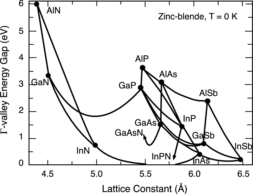
Lattice constant as a function of Γ-valley bandgap energy of zinc-blende structure III–V compound semiconductors at zero temperature. The bandgap energy of ternaries follows the line connecting the constituent binaries.
Reprinted with permission from [1], copyright AIP Publishing

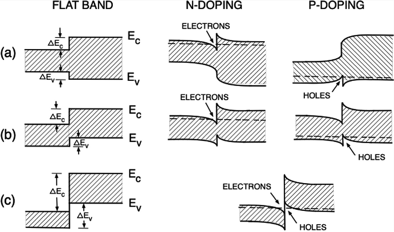
a Type I, b staggered type II, and c broken-gap type II band-edge alignments in semiconductor heterostructures. The energy band diagrams of flat band, n-type heterostructures, and p-type heterostructures are shown in the left, middle, and right panels, respectively
In 1952, the semiconductor nature of III–V compounds was first reported independently by Heinrich Welker of Siemens, West Germany, and a group at the Ioffe Institute, Russia. Inspired by the demonstration of the first laser, a solid-state ruby laser was developed in May 1960 by Theodore Maiman of the Hughes Research Laboratory, and three groups (GE, IBM, and MIT Lincoln Laboratory) independently demonstrated GaAs homojunction injection lasers in 1962 using diffused p–n junction structures. The first ternary alloy (GaAsP) laser emitting in the visible spectrum (710 nm) was also reported at about the same time by Nick Holonyak Jr. at GE. The next year, J. G. Gunn discovered microwave oscillation due to the transferred electron effect in direct bandgap III–V compounds. These important early inventions precisely highlight the strength of III–V semiconductor alloys over silicon—their light-emitting and high-speed properties.
Compared to silicon, compound semiconductors are more complex in terms of material preparation. Heterostructure devices are entrenched in the grown layer structures, not formed by post-growth diffusion processing commonly used in silicon IC fabrication. Thus, further advance of compound semiconductor technologies relies on the successful development of hetero-epitaxial growth technologies. For example, independently suggested by Herb Kroemer and Zhores Alferov in 1963, the incorporation of the double-heterojunction (DH) structure can improve the device efficiency of injection lasers. At the time, the threshold current density of GaAs injection lasers was nearly 105 A/cm2, which is too high even for room-temperature pulse operation. However, room-temperature cw DH laser operation was finally demonstrated in 1970 after the successful demonstration of the liquid phase epitaxy (LPE) technique to grow AlGaAs on GaAs in 1967. To improve the uniformity and growth rate control of LPE-grown layers, two major epitaxy techniques have been developed. Alfred Cho of Bell Laboratories pioneered the molecular beam epitaxy (MBE) technique and demonstrated MBE growth of AlGaAs and GaP in 1969. At Rockwell International, H. M. Manasevit first reported metalorganic chemical vapor deposition (MOCVD) of compound semiconductors on foreign substrates such as sapphire in 1968. With further developments, both MBE and MOCVD techniques have proved to have the characteristics of producing high-quality uniform multiple layered structures with excellent morphology, sharp interface, and precise doping and thickness control. These attributes ultimately formed the basis for successful growth of innovative bandgap-engineered devices with never-before-realized electrical and optical properties. In 1975, the quantum-well laser operation was demonstrated using MBE-grown AlGaAs/GaAs multilayer structures, where the quantum size effect occurred in very thin GaAs layers. The phrase quantum-well laser was first used in 1978 by Holonyak et al. to describe their MOCVD-grown laser structures. One additional advantage of these ultra-thin-layer structures is that high-quality strained layers can be achieved to further modify the energy band structure and enhance the laser performance. The ability to precisely make quantum wells has had a far-reaching impact, ranging from classroom physics to revolutions in electronic and optical devices for the consumer electronics, computers, and communications industries. Today, the global communication network relies on high-speed laser diodes and sensitive photodiodes to transmit and receive extremely high capacity information optically over hundreds of kilometers in low-loss optical fibers. High-electron-mobility transistors (HEMTs) are utilized as high-speed circuit components and in high-frequency, low-noise, direct broadcast satellite and wireless communications. The heterojunction bipolar transistor (HBT) is the key component to enabling the efficient performance and small size of cellular phones. Further development of these high-speed electronic devices will likely hasten the implementation of ultra-wide-bandwidth communication systems.
Another important development of compound semiconductor technology is the invention of the visible (red) light-emitting diode (LED) in 1962 by Holonyak using GaAsP ternary alloys. The performance (lumens/watt) of (As,P)-based LEDs increased 10 × per decade from 1970 to 2000 using GaP:Zn,O and GaP:N materials, and AlGaAs/GaAs and AlGaInP/GaAs heterostructures, progressively. However, the emission color of these LEDs was restricted by the bandgap energy of these alloys to between red and orange. Nevertheless, these LEDs have been used for many applications including instrument panels, displays, vehicle break lights, and traffic signals. In order to expand LED emissions to cover the full visible spectrum, specifically the blue–green band, GaN has been investigated since the early 1970s. However, the lack of suitable p-type dopants prevented it from forming useful p–n junction devices. In 1989, Isamu Akasaki and Hiroshi Amano of Nagoya University in Japan finally made the breakthrough; they obtained p-type conduction in Mg-doped GaN using post-growth annealing to remove hydrogen passivation and activate acceptors. This key discovery led Shuji Nakamura of Nichia in Japan to demonstrate the first InGaN/GaN blue LED grown by MOCVD. Now the LEDs with three primary colors are realized for making full-color displays. More important, white light LEDs for lighting applications are readily attainable using yellow-phosphorus-coated blue LEDs. As a general illumination lighting source, white light LED products surpass many conventional lighting technologies (including incandescent and fluorescent light sources) in energy efficiency, lifetime, and versatility and rival them in color and light quality. At the other end of the spectrum, innovative bandgap-engineered devices utilizing inter-subband transitions in quantum wells, such as quantum cascade (QC) lasers, extend the laser emission wavelength well into the mid-infrared (mid-IR), which is not available from bulk materials. Large area and uniform mid-IR quantum-well infrared photodetectors (QWIPs) based on the same inter-subband transitions were also developed. These mid-IR devices are critical for future planetary exploration, biomedical, and security applications.
1.2 Future Outlooks
Due to limitations in the material properties of silicon, III–V compound semiconductors have dominated photonic and high-speed electronic devices. This trend is likely to continue in the fast-growing wireless communications and Internet applications. The ability to form heterostructures further enhances the ability of compound semiconductors to form new quantum effect devices and efficient photonic devices. It is expected that III–V compound semiconductors will continue to thrive in high-speed, wide-bandwidth, and low-power consumption devices and circuits. In addition, the realization of the p-type GaN not only led to widespread applications of III-N-based LEDs for solid-state lighting and full-color displays but also enabled the development of next-generation power electronics using wide-bandgap semiconductors. The inherent properties of the bulk GaN, including a wide bandgap, higher electron mobility, and excellent thermal conductivity, allow III-N material-based power electronic devices to operate efficiently at higher voltages and power densities, higher frequency and temperature than silicon semiconductors, yielding significant energy savings. However, the realization of the full potential of wide-bandgap semiconductor-based power devices depends on the development of cost-effective substrates.

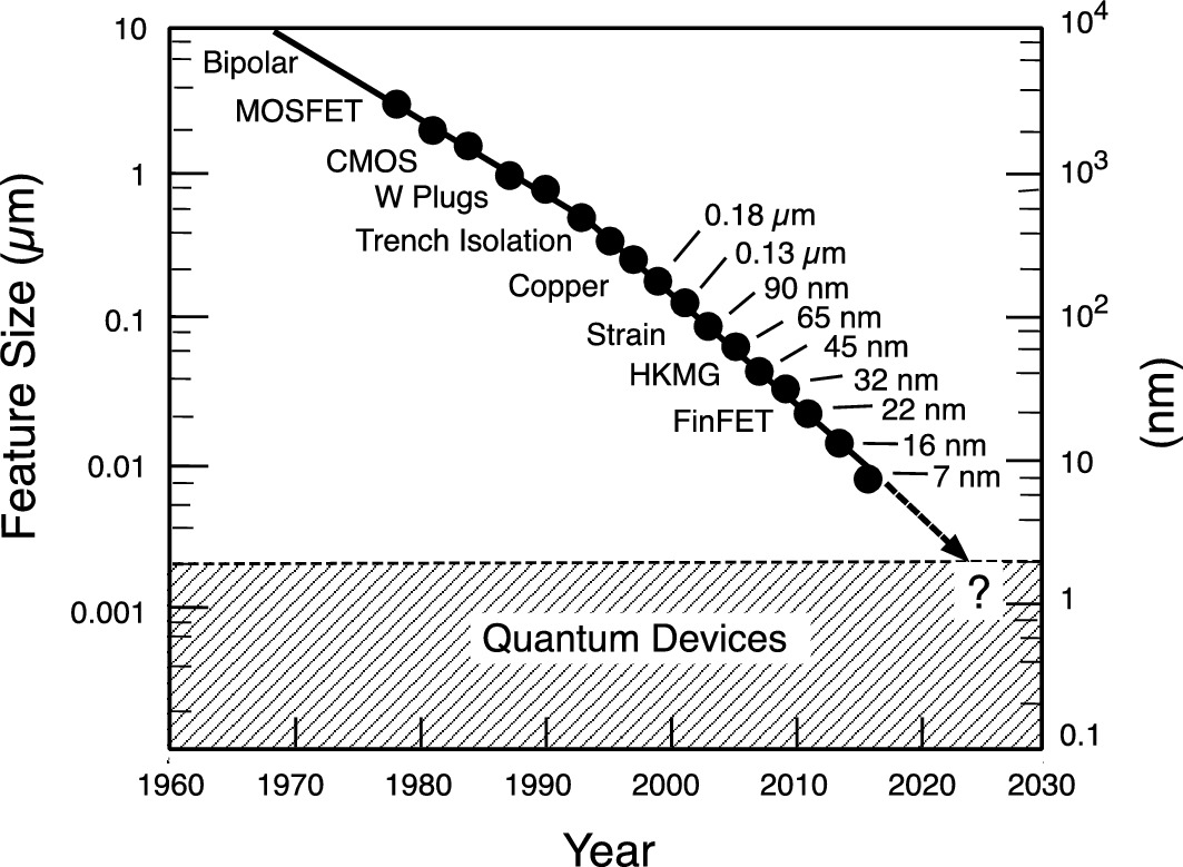
Feature size versus time in silicon ICs. Major device technology milestones are also listed