5
Semiconductor solar cells
In Chapter 4 we described the harvesting of solar energy by solar heaters where we use sunlight to heat a fluid. We saw that if the temperature of the heated fluid is sufficiently high, we can convert its thermal energy into electricity using the combination of a heat engine and an electrical generator. In this chapter we describe harvesting energy from the Sun using solar cells that exploit the photovoltaic effect. In this case, sunlight that is incident on a solar cell produces an electric current directly, i.e. without involving any thermal energy or indeed any moving parts. This is achieved using a semiconductor p–n junction. In this chapter, we describe the properties of semiconductors and the electrical characteristics of a p–n junction and how such a junction is employed in a solar cell.
5.1 Introduction
The discovery of the photovoltaic effect in 1839 is credited to Edmond Becquerel. He was the father of Henri Becquerel, whom we encountered in our discussion of radioactivity in Chapter 2. He observed that when an acid solution containing silver chloride was exposed to light, a current flowed between platinum electrodes inserted into the solution. The conversion of light into electricity using a solid material (selenium) was first demonstrated by William Grylls Adams and Richard Evans Day in 1875. Some years later (1894), Charles Fritts constructed what was probably the first true solar cell. He coated the semiconductor selenium with a thin layer of gold. The efficiency of his solar cell for converting sunlight into electrical energy was only about 1%, so that it could not be used to generate electrical power economically. However, the selenium cell went on to find widespread use as a light meter in photography. The important breakthrough came in the 1950s at the Bell Laboratories, USA. There, Gerald Pearson, Darryl Chapin and Calvin Fuller demonstrated a solar cell using doped silicon, which is also a semiconductor. It had an efficiency of 5.7% and made possible the development of the solar cell as a viable source of energy.
We can compare the photovoltaic effect with the more familiar photoelectric effect. In the photoelectric effect, ultraviolet (UV) light that is incident upon a metal surface liberates photoelectrons from the surface. (Photoelectrons are no different from any other electrons but take this name when we talk about their generation by photons.) Einstein received the Nobel Prize in 1923 for his explanation of the photoelectric effect in terms of quanta of energy, which we now call photons and which we discussed in Section 4.2.3. Einstein's equation that describes the photoelectric effect is
where hν is the photon energy, φ is the work function of the metal and Emax is the maximum energy that a generated photoelectron can have. Clearly, hν must be larger than φ, which is typically ∼5 eV for a metal. For example, the work function of gold is 5.1 eV and incident photons must have a wavelength shorter than 243 nm to liberate photoelectrons from a gold surface.
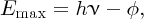
A schematic diagram of an apparatus for observing the photoelectric effect is shown in Figure 5.1. UV light is incident upon the metal surface. An electrode is placed in front of the surface and is held at a positive potential with respect to it. The potential difference produces an electric field that directs the emitted photoelectrons to the positively charged electrode and the electrons flow in the external circuit producing a current i. (Note that conventional current flows in the opposite direction to electron flow.) Although this arrangement does not produce electrical power economically, it is widely used to measure the irradiance of UV light in research applications.
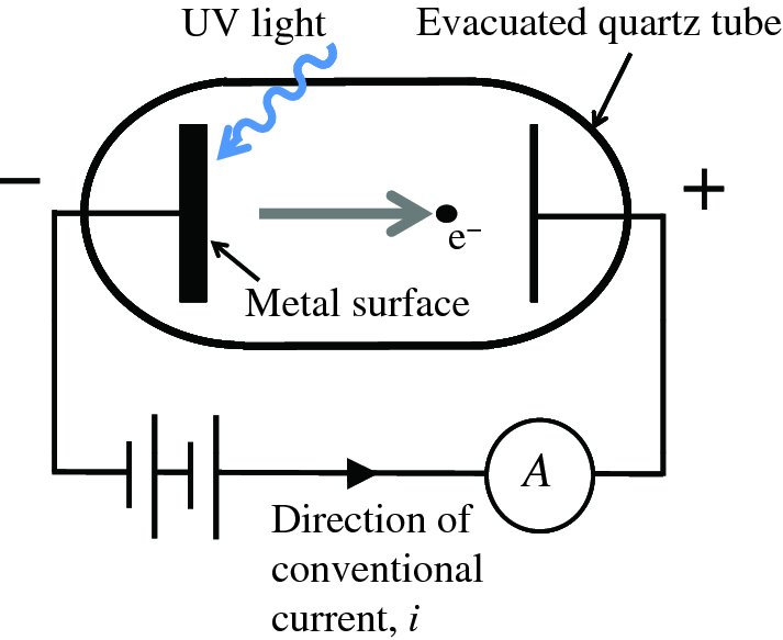
Figure 5.1 The photoelectric effect in which UV light is incident upon a metal surface. An electrode is held at a positive potential with respect to the metal surface and collects emitted photoelectrons, which then flow in the external circuit, producing a current i. (Note that conventional current flows in the opposite direction to electron flow.)
The photovoltaic effect has some similarities with the photoelectric effect. Now, however, the process occurs in or close to the depletion layer that exists at a p–n junction in a semiconductor material. Figure 5.2 is a schematic diagram of a solar cell showing the depletion layer between the p and n regions. Again, there is an incident photon, but now the resulting electron is not ejected from the surface but is promoted to a higher-lying energy level in the semiconductor, which enables it to move freely through the semiconductor material. The excited electron leaves behind a vacancy or hole in the semiconductor material, so that the incident photon produces an electron–hole pair. Importantly, there is an inbuilt electric field across the depletion region and, consequently, there is no need for an externally applied voltage to cause a current flow. This electric field causes the electron–hole pair to separate and the electron to move to the n region and the hole to move to the p region. A metallic grid forms one of the electrodes of the cell, and a metallic layer on the back of the solar cell forms the other electrode. If these are connected to an external load, electrons generated by photons incident on the cell flow around the external circuit from the n region to the p region where they combine with generated holes. In this way, electrical power is delivered to the external load.
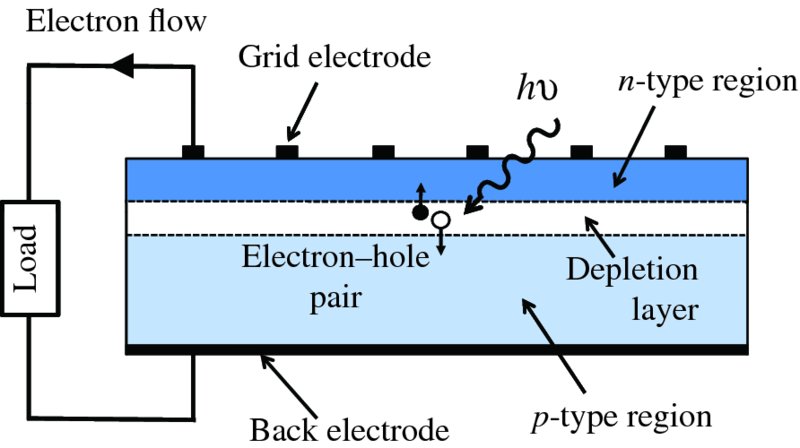
Figure 5.2 Schematic diagram of a solar cell, which is formed from a p–n junction in a semiconductor material. Incident photons cause the generation of electron–hole pairs in or close to the depletion layer that exists at the junction. There is an inbuilt electrical field across the depletion layer that causes the electrons to move into the n-type material and the holes to move into the p-type material. Electrons generated by the incident photons flow around the external circuit from the n-type to the p-type, where they combine with the holes. In this way, electrical power is delivered to an external load.
An incident photon must have sufficient energy to generate an electron–hole pair. We will see that this means the photon must have an energy, hν, that is greater than the band gap, Eg, of the semiconductor material:

The band gap of a semiconductor is ∼1 eV, e.g. Eg = 1.11 eV for silicon. We saw in Chapter 4 that the majority of the photons in the solar spectrum have energies >1 eV, and so semiconductor solar cells provide a valuable way to harvest solar energy. To understand the action of a solar cell more fully, we begin with a discussion of semiconductor materials.
5.2 Semiconductors
Conductors and insulators are distinguished by the enormous differences in their electrical resistivities. For example, the resistivity of quartz is ∼1025 times larger than the resistivity of copper. Lying between insulators and conductors with respect to resistivity are semiconductors. For example, the resistivity of the semiconductor silicon is about 1010 times larger than that for copper. The reason for such enormous differences is the variation in the number of free electrons that can carry electric current in these kinds of material. These variations arise because in a crystalline solid, such as quartz, copper or silicon, the electrons can only exist in allowed energy bands. What is important is the extent to which these bands are occupied by electrons and the energy gaps between adjacent bands.
5.2.1 The band structure of crystalline solids
The energy levels in an isolated atom are discrete and well separated from each other. For example, the energy separation between the two lowest energy levels of hydrogen, with values of principal quantum number n of 1 and 2, respectively, is 3.4 eV. If two identical atoms are brought into close proximity to each other, their energy levels change as their electronic wave functions begin to overlap. As a result, each atomic energy level splits into two levels of slightly different energy for the two-atom system. Similarly, if we bring four atoms into close proximity, a particular energy level splits into four separate energy levels with slightly different energies, which belong to the collection of the four atoms as a whole. When we have N atoms in close proximity, as in a crystal lattice, each energy level of the isolated atom splits into N different energy levels. A macroscopic solid contains ∼1023 atoms/mole and so each particular atomic energy level splits into a very large number of densely packed levels. The energy levels are so numerous and so closely spaced that for all practical purposes they are indistinguishable from a continuous energy band. This evolution of energy levels into energy bands is illustrated in Figure 5.3. The energy bands are typically a few eV wide. They may be widely separated in energy, they may be close together or, indeed, they may overlap. It depends on the atoms and the way in which the atoms bond together. The energy gaps between these allowed bands are called forbidden energy gaps, since an electron in the solid cannot have an energy that lies within these gaps.
Figure 5.3 Schematic representation of how energy levels of closely spaced atoms evolve into energy bands. The energy gaps between the allowed bands are called forbidden energy gaps because an electron cannot have an energy that lies within these gaps.
The energy levels in the allowed bands are filled with the atomic electrons according to the Pauli exclusion principle, which states that only one electron can occupy a given quantum mechanical state. Electrons are fermions that can have two values of spin quantum number s. Hence, each discrete energy level can contain two electrons at most. The energy bands are filled, starting with the lowest energy band, then the next higher energy band and so on until all the electrons are accommodated. The electrons in the lowest bands are tightly bound and are generally not important in determining the electrical (or chemical) properties of a solid. The two highest energy bands in a solid are called the valence band and the conduction band. They are separated in energy by the band gap Eg. In a particular solid, the valence band may be completely filled, or partly filled with electrons, while the conduction band is never more that slightly filled. The extent to which these bands are filled and the size of the band gap, Eg, between them determines whether a solid is a conductor, an insulator or a semiconductor.
When an electron is under the influence of an electric field, it is accelerated by that field and gains energy from it. Classically the electron can gain any amount of energy. It is equal to eV, where V is the voltage drop across the region of acceleration. This would be the case, for example, for an electron being accelerated in an X-ray tube. In a system governed by quantum mechanics, however, an electron can only gain quantised amounts of energy corresponding to differences between the energy levels of the system. When current flows through a solid, the electrons gain energy from the applied electric field and, in so doing, are excited into higher-lying levels in an allowed band. However, current can only flow if energy levels are available for the electrons to be excited into.
Suppose that the valence band in a solid is only partially full when all the electrons have been accommodated, as in Figure 5.4(a). Then there are many empty levels into which an electron can be promoted. Consequently electrons can readily gain energy from an electric field and the result is that the solid has high electrical conductivity. Sodium provides an example of a partially filled valence band. Sodium has 11 electrons and these are arranged in electronic sub-shells according to 1s2 2s2 3p6 3s1, which is a shorthand notation to identify the sub-shells. For example, the 3p sub-shell (with principal quantum number n = 3 and orbital quantum number l = 1) contains six electrons as specified by the numerical superscript. The single 3s electron is relatively loosely bound in the sodium atom and it is this electron that takes part in electrical conductivity. Electrons in the other sub-shells are so tightly bound to the nucleus that they do not take part. When N atoms of sodium come together to form a crystalline solid, the 3s energy level splits into N energy levels, each of which can accommodate two electrons. (The factor of 2 arises because of the two possible spin states of the electrons.) As the number of 3s valence electrons arising from the N atoms is just N, it follows that only half of the possible energy levels in the valence band due to the 3s atomic level will be occupied. Consequently, these electrons can readily gain energy from an external field and the result is that sodium has high electrical conductivity. In some other metals, such as magnesium, the valence and conduction bands overlap, as shown in Figure 5.4(b). Again this provides many energy levels for electrons to be excited into by an electric field and such metals also have high electrical conductivity.
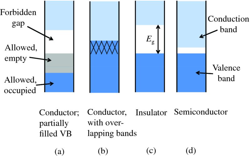
Figure 5.4 Electronic band structures for: (a) a typical conductor like sodium in which the valence band is partially full; (b) a conductor like magnesium in which the allowed energy bands overlap; (c) a typical insulator, where there is a large forbidden energy gap between the valence and conduction bands; and (d) a semiconductor where the forbidden energy gap is small.
Suppose that in a solid the electrons completely fill all the allowed energy bands up to and including the valence band and that the conduction band is empty at absolute zero, T = 0 K. This case is shown in Figure 5.4(c), where the band gap Eg is relatively large. When we apply an electric field, the electrons cannot be excited into higher energy levels in the valence band as all the levels in that band are already occupied. Moreover, electric fields of normal strength do not provide electrons with enough energy to be promoted into the conduction band. The electrons have nowhere to be excited to and the solid is an insulator.
Now at any temperature T above absolute zero, there is a finite probability that an electron can be promoted
from the valence band into the conduction band. This is because it has thermal energy ∼kT, where k is the Boltzmann constant. The probability is given approximately by the Boltzmann factor
 (see Section 5.3.3). An example of an electrical insulator is diamond. Its valence
band is full and the band gap Eg is 5 eV. We recall that kT = 1/40 eV at room temperature. Hence, we find that the probability of an electron
being excited into the conduction band at room temperature is about 10− 87. This is an extremely small number and, indeed, diamond is a very good insulator.
(see Section 5.3.3). An example of an electrical insulator is diamond. Its valence
band is full and the band gap Eg is 5 eV. We recall that kT = 1/40 eV at room temperature. Hence, we find that the probability of an electron
being excited into the conduction band at room temperature is about 10− 87. This is an extremely small number and, indeed, diamond is a very good insulator.
In the case of a semiconductor at absolute zero, the valence band is full and the conduction band is empty and under this condition, a semiconductor is an insulator. However, the energy gap between the valence and conduction bands is much smaller than for an insulator, as indicated by Figure 5.4(d); for the semiconductor germanium, the band gap Eg is 0.67 eV. Such a band gap is sufficiently small that an appreciable number of electrons do have enough thermal energy to be promoted into the conduction band at room temperature, as illustrated by Figure 5.5. The conduction band contains a very large number of empty levels that these electrons can be excited into by an applied electric field, so that these electrons are free to move through the semiconductor under the influence of the electric field. Hence, germanium becomes reasonably conductive at room temperature, although still far less conductive than, say, copper.
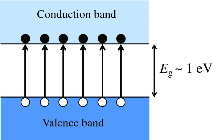
Figure 5.5 Generation of electron–hole pairs by thermal excitation of electrons from the valence band to the conduction band of a semiconductor. The electrons that are excited to the conduction band leave behind holes in the valence band.
The electrons in a semiconductor that are thermally excited to the conduction band leave behind vacancies or holes in the valence band (see Figure 5.5). As the electrons and holes are produced in pairs, the concentration of electrons in the conduction band and the concentration of holes in the valence band must be equal. As an electron moves through the semiconductor, it may encounter a hole. If it does, the electron and hole recombine and disappear. At equilibrium, the rate of recombination must be equal to the rate of generation of electron-hole pairs.
The hole in a particular atom of the semiconductor may be filled by an electron from a neighbouring atom so that the hole has moved from the first atom to the second. Then an electron from a third atom may fill the second hole and the process repeats from atom to atom. If a voltage is applied to the semiconductor, as in Figure 5.6, the electrons will move towards the positive end, while the holes will appear to move in the opposite direction, to the negative end. Although only electrons are moving in the crystal, it is convenient to consider the hole as a particle with positive charge +e that is capable of moving in a similar manner to electrons but in the opposite direction. Because the holes are positively charged, the flow of holes in one direction is equivalent to a flow of electrons in the opposite direction. Hence, the net current in the semiconductor is the sum of the electron and hole currents. This is indicated in Figure 5.6, where the direction of the net current points in the direction of the electron flow. (We will consistently use the convention where the net current is in the same direction as the electron current.) Electrons leave the positive end of the semiconductor, travel around the external circuit and re-enter the semiconductor at the negative end, where they recombine with holes.
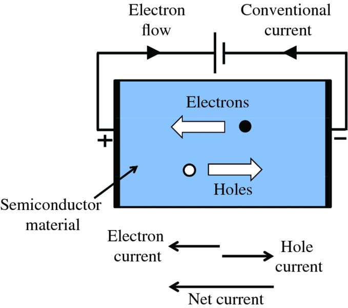
Figure 5.6 If a potential difference is applied across a semiconductor, the free electrons move toward the positive end, while holes appear to move in the opposite direction towards the negative end. Because the holes are positively charged, the flow of holes in one direction is equivalent to a flow of electrons in the opposite direction. Hence, the net current in the semiconductor is the sum of the electron and hole currents.
5.2.2 Intrinsic and extrinsic semiconductors
Our discussion of semiconductors so far has been for pure elements such as pure silicon and pure germanium. These are called intrinsic semiconductors. We saw that at temperatures above absolute zero, such intrinsic semiconductors have a finite number of thermally generated electrons in the conduction band and holes in valence band. However, the densities of these charge carriers are small because the thermal energy ∼kT of the electrons is small compared with the band gap energy Eg. The number of charge carriers in a semiconductor can be increased enormously by introducing impurities into it in a process called doping. In this process, some of the semiconductor atoms in the crystal lattice are replaced by impurity atoms. By suitable choice of impurity, the number of electrons or the number of holes can be increased. A semiconductor in which the number of electrons has been increased is called n-type, where n stands for negative charge carriers, while a semiconductor where the number of holes has been increased is called p-type, where p stands for positive charge carriers. Such a doped material is called an extrinsic semiconductor. As for the case of intrinsic semiconductors, electron-hole pairs are also created in an extrinsic semiconductor by thermal excitation of electrons across the band gap. However, the concentrations of these thermally generated charge carriers are extremely small compared with the concentration of charge carriers due to the added impurities. The more abundant charge carriers in a semiconductor are called majority carriers. In n-type semiconductors they are electrons and in p-type semiconductors, they are holes. The less abundant charge carriers are called minority carriers. In n-type semiconductors they are holes, and in p-type semiconductors, they are electrons.
n -type semiconductors
The silicon atom has 14 electrons and these are arranged in various electronic sub-shells as shown in Table 5.1. Four of these electrons take part in bonding with other silicon atoms: the two 3s and the two 3p electrons. The form of bonding in the crystal lattice is called covalent bonding where a silicon atom shares one of its electrons with another silicon atom that also contributes an electron to the sharing process. Thus a silicon atom is surrounded by four other silicon atoms, leading to the crystal structure of silicon. A two-dimensional representation of this crystal structure is illustrated in Figure 5.7.
Table 5.1 Electronic configuration of aluminium, silicon and phosphorus
| Atom | Electronic configuration |
| Aluminium, Z = 13 | 1s2 2s2 2p6 3s2 3p1 |
| Silicon, Z = 14 | 1s2 2s2 2p6 3s2 3p2 |
| Phosphorus, Z = 15 | 1s2 2s2 2p6 3s2 3p3 |
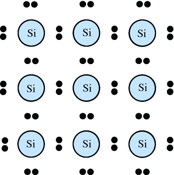
Figure 5.7 A two-dimensional representation of the crystal structure of silicon. Each silicon atom is surrounded by four other silicon atoms and shares one of its electrons with one of its neighbours, which also contributes an electron to this sharing process.
Suppose now that we introduce an atom of phosphorus so that it takes the place of a silicon atom in the lattice, as shown in Figure 5.8. Phosphorus has one more electron than silicon, as shown in Table 5.1; there are two 3s and three 3p electrons. Consequently, one of the electrons from the phosphorus atom will be left over, i.e. it will be spare with no partner to form a covalent bond (see Figure 5.8). This spare electron then becomes only weakly bound to the phosphorus atom and so is easily freed from it. This free electron can then roam through the lattice and conduct electrical current under the influence of an electric field. Impurity atoms that donate spare electrons in this way are called donor atoms. They convert a pure (intrinsic) semiconductor into an n-type (extrinsic) semiconductor.
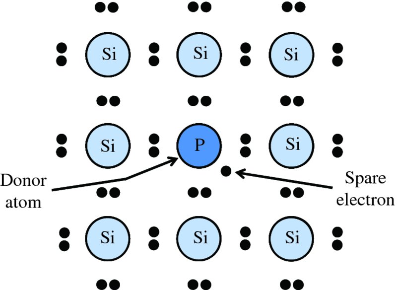
Figure 5.8 Creation of a spare electron in the crystal lattice of silicon by a donor impurity atom of phosphorus, which has one more electron than silicon.
Ed is the amount of energy it takes to remove the weakly bound electron from a phosphorus atom and allow it to become a conduction electron. Equivalently, we can say that this is the amount of energy required to lift the electron into the conduction band. Therefore, these weakly bound electrons must reside in energy levels that lie just below the conduction band, by the amount Ed. This, indeed, is the situation at absolute zero (T = 0 K) and is illustrated in Figure 5.9(a). The energy levels are called donor energy levels. As noted above, at room temperature (T ∼ 300 K) essentially all the electrons in the donor levels are promoted into the conduction band, as illustrated in Figure 5.9(b).
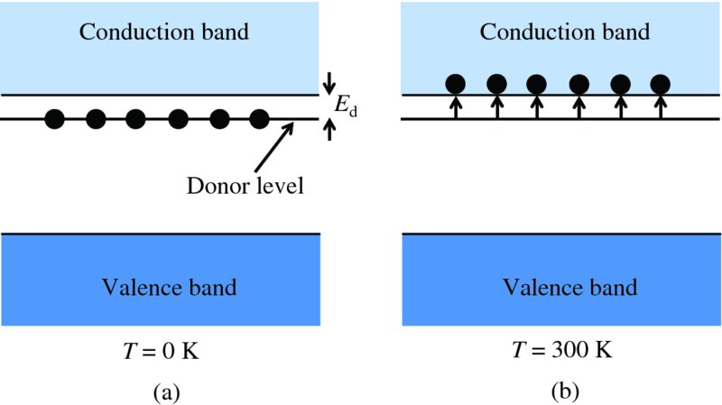
Figure 5.9 (a) In an n-type semiconductor at absolute zero (T = 0 K), all the electrons that are bound to the donor atoms are in donor levels that lie just below the bottom of the conduction band. (b) At temperatures above absolute zero, these weakly bound electrons can be thermally excited into the conduction band and, at room temperature (300 K), essentially all these electrons are promoted into the conduction band.
p-type semiconductors
A complementary situation occurs in a p-type semiconductor. Suppose that we introduce an atom of aluminium into the crystal lattice so that it takes the place of a silicon atom, as shown in Figure 5.10. Aluminium has one less electron than silicon, as shown in Table 5.1; it has two 3s electrons and just one 3p electron. Consequently, it has only three electrons to share with its four neighbouring silicon atoms, which means that one of the four valence bonds is incomplete. In order to complete this bond, the aluminium atom accepts an electron from one of its silicon neighbours, as illustrated in Figure 5.10. This creates a hole in the neighbouring silicon atom. As we saw previously, such a hole acts as a positive charge carrier that can move freely through the crystal under the influence of an electric field. As the impurity atom has gained an extra electron it becomes a negatively charged ion, Al−, which is fixed in the crystal lattice. Because the impurity atom accepts an electron from a neighbouring silicon atom, it is called an acceptor atom.
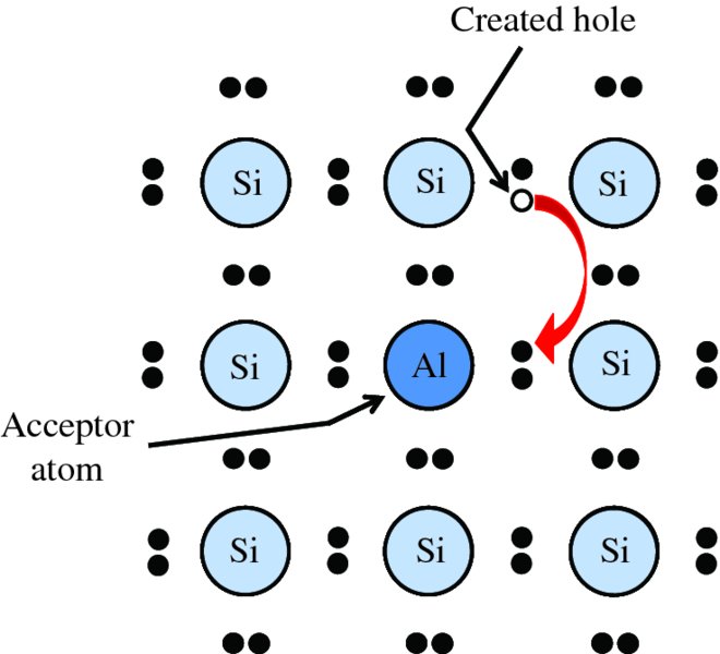
Figure 5.10 Creation of a hole in the crystal lattice of silicon by an acceptor impurity atom of aluminium, which has one less electron than silicon. The aluminium atom accepts an electron from a neighbouring silicon atom to complete the valence bond, thus creating the hole at the site of that silicon atom.
It needs a small but finite amount of energy Ea for an electron to transfer from a silicon atom to an aluminium atom. Equivalently we can say that Ea is the amount of energy required to generate a hole in the valence band. It follows that the energy level associated with such a transfer must lie at a distance Eg above the top of the valence band, as shown in Figure 5.11(a). And when an electron transfers from a silicon atom to an aluminium atom, it jumps from the valence band into this energy level. As it accepts an electron, it is called an acceptor level. At absolute zero, the electrons do not have the necessary thermal energy to make the transfer and remain in the valence band as in Figure 5.11(a). By similar reasoning to that used for n-type semiconductors, we find that Ea ∼ 10 meV. Again, this is substantially smaller than kT at room temperature, and, at that temperature, essentially almost all of the acceptor levels are filled, as indicated in Figure 5.11(b). Then the number of holes is essentially equal to the number of added impurity atoms.
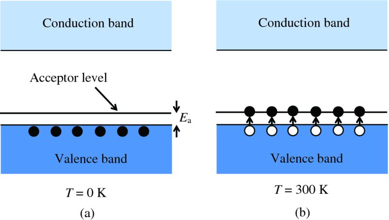
Figure 5.11 (a) In a p-type semiconductor at absolute zero (T = 0 K), the electrons remain in the valence band. (b) At temperatures above absolute zero, the electrons can be thermally excited into acceptor levels that lie just above the top of the valence band. This creates holes in the valence band.
5.3 The p–n junction
A solar cell is essentially a p–n junction. Indeed, the p–n junction is at the heart of essentially all semiconductor devices, including diodes, transistors and light-emitting diodes (LEDs). Such a junction is formed when an n-type semiconductor meets a p-type semiconductor. In this section we describe the movement of electrons and holes across a p–n junction and the resulting electrical properties of the junction.
5.3.1 The p–n junction in equilibrium
Consider first two isolated pieces of semiconductor material, a p-type and an n-type, as shown in Figure 5.12. In this figure, only the acceptor and donor ions and the respective majority carriers
are shown. The acceptor and donor ions are denoted by the symbols
 and
and
 respectively. In the p-type there is an abundance of holes, which form the majority carriers. These are
denoted by the ‘+’ symbol. There is charge neutrality because of the presence of the
negatively charged acceptor ions that are embedded uniformly throughout the lattice.
Similarly, in the n-type, there is an abundance of electrons, which are the majority carriers, denoted
by the ‘−’ symbol, and there are positively charged donor ions that are uniformly
embedded in the lattice; again there is charge neutrality. In general, the concentration
of holes in the p-type will be different from the concentration of electrons in the n-type.
respectively. In the p-type there is an abundance of holes, which form the majority carriers. These are
denoted by the ‘+’ symbol. There is charge neutrality because of the presence of the
negatively charged acceptor ions that are embedded uniformly throughout the lattice.
Similarly, in the n-type, there is an abundance of electrons, which are the majority carriers, denoted
by the ‘−’ symbol, and there are positively charged donor ions that are uniformly
embedded in the lattice; again there is charge neutrality. In general, the concentration
of holes in the p-type will be different from the concentration of electrons in the n-type.
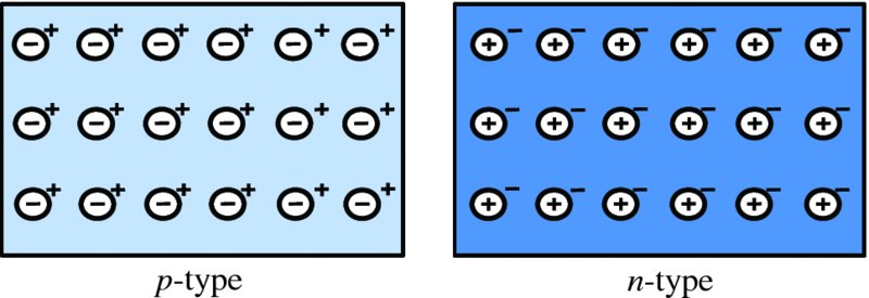
Figure 5.12 The figure shows isolated pieces of p-type and n-type semiconductor. For the sake of clarity, only the acceptor and donor ions and
the respective majority carriers are shown. The acceptor and donor ions are denoted
by the symbols
and
respectively. In the p-type, there is an abundance of holes, which form the majority carriers. These are
denoted by the ‘+’ symbol. Similarly in the n-type, there is an abundance of electrons, which are the majority carriers, denoted
by the ‘−’ symbol. In general, the concentration of holes in the p-type will be different from the concentration of electrons in the n-type.
Imagine that we join these two pieces of semiconductor material together, as shown in Figure 5.13. As there are many more free electrons in the n-type than in the p-type, electrons will diffuse from the n-type into the p-type. Similarly, holes in the p-type will diffuse into the n-type. An analogy here is a box that is divided into two halves by a barrier. Imagine that the left side is filled with oxygen and the right side is filled with nitrogen. If the barrier is permeable, oxygen diffuses to the right and nitrogen diffuses to the left. The diffusion of these majority charge carriers across a p–n junction gives rise to the so-called diffusion current, idiff, which is the net current due to the movement of both the electrons and the holes. In Figure 5.13, this diffusion current is represented by an arrow, which points in the same direction as conventional current flow.
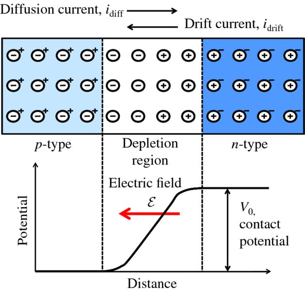
Figure 5.13 The p–n junction in equilibrium. Diffusion of electrons and holes across the junction and
their subsequent recombination produce a depletion layer that is devoid of mobile
charge carriers. When electrons diffuse away from the n-type region, they leave behind positively charged donor ions. Similarly, when holes
diffuse away from the p-type region they leave behind negatively charged acceptor ions. This double layer
of charge causes an electric field
 to be set up across the junction, producing a difference in potential energy between
the n and p regions. This produces a potential barrier of height, V0, that inhibits holes from the p region diffusing into the n region and similarly inhibits electrons diffusing into the p region. At equilibrium, there must be no net current flow across a p–n junction. Hence, the drift current, idrift, is exactly counterbalanced by the diffusion current idiff, as indicated by their respective arrows on the figure.
to be set up across the junction, producing a difference in potential energy between
the n and p regions. This produces a potential barrier of height, V0, that inhibits holes from the p region diffusing into the n region and similarly inhibits electrons diffusing into the p region. At equilibrium, there must be no net current flow across a p–n junction. Hence, the drift current, idrift, is exactly counterbalanced by the diffusion current idiff, as indicated by their respective arrows on the figure.
As free electrons from the n-type diffuse into the p-type, they recombine with holes in the p-type that are present in high concentration and so move only a short distance before disappearing. Similarly, holes in the p-type diffusing across the junction recombine with electrons in the n-type. As a result of the electrons and holes recombining in this way, there is a depletion layer at the p–n junction that is depleted of mobile charge carriers. When the electrons diffuse away from the n-type they leave behind positively charged donor ions that are fixed in the lattice. Thus a layer of positive charge is built up on the n side of the junction. Similarly, a layer of negative charge is built up on the p side of the junction due to the negatively charged acceptor ions; the resulting ions that have lost electrons or holes are said to be uncovered. The diffusion of electrons and holes thus creates a double layer of charge. The positive charge layer on the n side repels holes and the negative charge layer on the p side repels electrons, and further diffusion of the electrons and holes is inhibited.
The double-charge layer sets up an electric field
 that points from the n side to the p side of the junction. This is the origin of the inbuilt electric field of a p–n junction. And it leads to a difference in potential energy between the n-type and p-type; the n-type is at the higher potential, as shown in Figure 5.13. We can then picture the
resulting situation in terms of a potential barrier of height V0 that inhibits holes from the p region diffusing into the n region, at higher potential, and also inhibits electrons diffusing into the p region. The height of the barrier V0 is called the contact potential. Its value depends on the levels of doping and the temperature and is typically ∼0.5 V. We emphasise that this is an internal barrier. It is not an externally imposed barrier but is a property of the p–n junction itself.
that points from the n side to the p side of the junction. This is the origin of the inbuilt electric field of a p–n junction. And it leads to a difference in potential energy between the n-type and p-type; the n-type is at the higher potential, as shown in Figure 5.13. We can then picture the
resulting situation in terms of a potential barrier of height V0 that inhibits holes from the p region diffusing into the n region, at higher potential, and also inhibits electrons diffusing into the p region. The height of the barrier V0 is called the contact potential. Its value depends on the levels of doping and the temperature and is typically ∼0.5 V. We emphasise that this is an internal barrier. It is not an externally imposed barrier but is a property of the p–n junction itself.
As well as the majority charge carriers (electrons in the n-type and holes in the p-type), we recall that there are also minority carriers that are produced when thermal excitation generates electron–hole pairs. These are generated in both the n- and p-type regions. In the n-type, the generated holes are the minority carriers, and in the p-type the generated electrons are the minority carriers. Those minority carriers formed close to the p–n junction may migrate towards the junction and will be swept across it by the junction field; the direction of the field causes the generated electrons to drift toward the n side and the holes to drift toward the p side. The current due to these minority carriers is called the drift current, idrift, and is the sum of the electron current in one direction and the hole current in the other. In Figure 5.13, this drift current is represented by an arrow, which points in the opposite direction to the diffusion current.
At equilibrium, there must be no net current flow across a p–n junction. Hence, the small idrift due to thermal generation must be exactly counterbalanced by a finite idiff. Thus, although the junction field inhibits the majority carriers from diffusing across the junction, there nevertheless remain a relatively small number of them that must do so. In fact, the contact potential V0 adjusts until the drift and diffusion currents cancel exactly. Then for a p–n junction in equilibrium, the diffusion and drift currents are equal in magnitude but flow in opposite directions, as indicated by their respective arrows on Figure 5.13; the lengths of the arrows, which represent the magnitudes of the diffusion and drift currents, are equal but the arrows point in opposite directions.
It was convenient to think in terms of bringing together a piece of p-type semiconductor and a piece of n-type semiconductor to form a junction between the two. However we cannot just push pieces of p- and n-type semiconductor together and expect the junction to work properly because of the impossibility of achieving a continuous crystal structure across the junction. Instead, impurity atoms are added to a single piece of semiconductor. This can be done by first heating a slice of a pure silicon crystal, ∼300 μm thick, to a temperature of ∼1000 °C in a vacuum chamber while passing P2O5 gas over one of its surfaces. Phosphorus atoms diffuse into the surface, producing a thin layer of n-type material. The process is continued until the desired thickness of the n-type material is obtained. Then, the p-type layer is made by diffusing aluminium into the other surface of the silicon crystal. This is continued until the desired width of the p-type material is obtained and the p–n junction is formed.
5.3.2 The biased p–n junction
The p–n junction with reverse bias
Reverse bias is applied to a p–n junction, as shown in Figure 5.14, where the negative terminal of a battery is connected to the p side and the positive terminal to the n side. The effect of this bias voltage is to attract away from the junction both holes in the p region and electrons in the n region. This increases the number of donor ions and acceptor ions near the junction that are left uncovered and increases the width of the depletion layer. As the depletion layer is depleted of charge carriers, its resistance is much greater than that of the p or n regions. Consequently, most of the bias voltage V occurs across the depletion layer. The action of this bias voltage is to increase the height of the potential barrier from V0 to (V0 + V). This further inhibits the flow of majority carriers across the junction and reduces the diffusion current to essentially zero, as indicated by the reduced length of the diffusion current arrow in Figure 5.14. However, there will still be thermally generated electron–hole pairs in the n and p regions; the number of these pairs depends on the temperature and the band gap of the semiconductor and these remain the same. And those minority carriers generated close to the junction may migrate towards the junction and will be swept across the depletion layer by the junction field. Hence, the drift current idrift will still exist. The magnitude of this current does not depend appreciably on the applied bias potential, V. Hence, the length of the arrow representing the drift current in Figure 5.14 is essentially the same length as for the p–n junction in equilibrium, with no bias voltage applied.
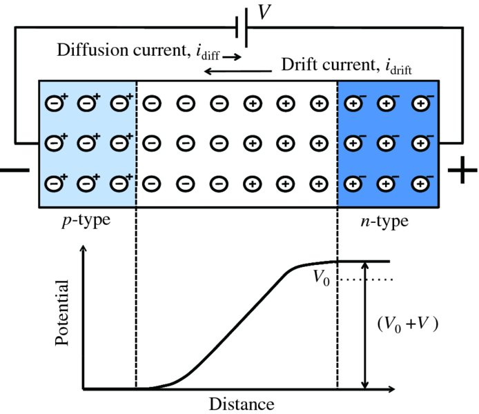
Figure 5.14 A reverse-biased p–n junction. The effect of the bias voltage V is to push the majority charge carriers away from the junction, increasing the width of the depletion region. The bias voltage V is dropped across the high-resistance depletion layer, increasing the height of the potential barrier from V0 to (V0 + V) and reducing the diffusion current to essentially zero. The drift current due to thermally generated electron–hole pairs is essentially insensitive to the bias voltage and remains the same as for the p–n junction in equilibrium. Thus the arrow representing the diffusion current is much reduced in length but the length of the drift arrow remains the same.
The p–n junction with forward bias
Forward bias is applied to a p–n junction as shown in Figure 5.15, where the positive terminal of a battery is connected to the p side and the negative terminal to the n side. The effect of this is to push towards the junction the electrons in the n region and the holes in the p region. This decreases the number of donor ions and acceptor ions near the junction that are left uncovered and reduces the width of the depletion layer. Again, the bias voltage V is dropped almost entirely across the high-resistance depletion layer and has the effect of lowering the height of the potential barrier to (V0 − V). This lowering of the barrier means that more majority carriers can surmount the barrier, i.e. diffuse across the junction. As the applied voltage increases, an increasing number of majority carriers diffuse across the junction and by V ∼0.5 V there is an appreciable diffusion current flowing across the junction. This is indicated in Figure 5.15 by the increased length of the arrow representing the diffusion current. As before, those minority carriers that are formed close to the junction may migrate towards it and be swept across the junction by the inbuilt electric field and so again the drift current does not change appreciably.
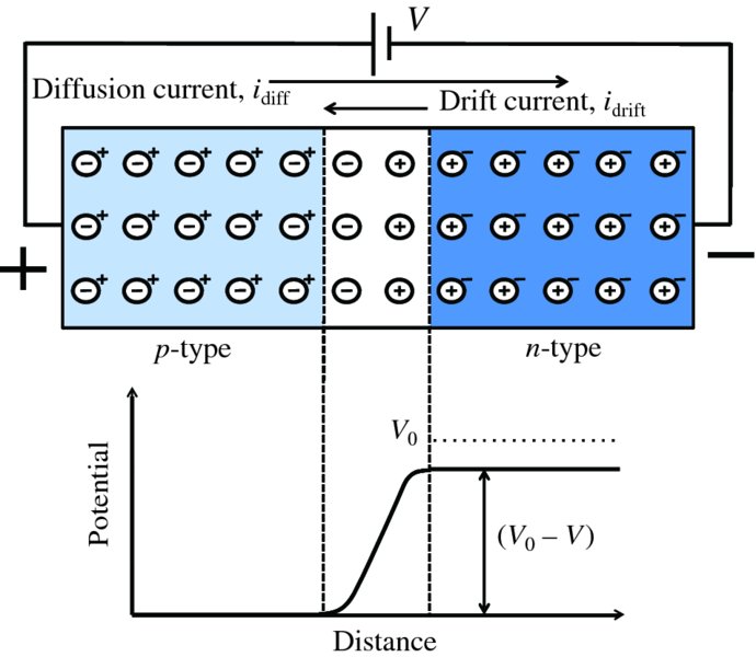
Figure 5.15 A forward-biased p–n junction. The effect of the bias voltage V is to push the majority carriers toward the junction, reducing the width of the depletion region. The bias voltage is again dropped across the depletion layer and has the effect of reducing the height of the potential barrier to (V0 − V), so that more majority carriers can surmount the reduced barrier. This increases the diffusion current, which becomes larger than the drift current, as indicated by the length of the respective arrows.
The electrons do not travel far into the p-type before they recombine with a hole, which are plentiful there. The characteristic distance they travel is called the diffusion length. Similarly, the holes have a diffusion length, which is characteristic of the distance they travel in the n-type before recombining with an electron. In general the diffusion length for the holes will be different from that for the electrons. In the p-type, the resultant flow of holes towards the junction is equivalent to a flow of electrons in the opposite direction. These electrons leave the p-type to flow through the external circuit and flow back into the n-type to neutralise the holes that have diffused into the n-type. When a majority charge carrier crosses the p–n junction, it becomes a minority charge carrier. Thus we see that it is the flow of minority carriers (holes in the n-type and electrons in the p-type) that account for the flow of current in a p–n junction.
Figure 5.16 summarises the currents that flow across a p–n junction for the three possible bias conditions. These are the diffusion current due to the diffusion of majority carriers across the junction and the drift current due to the minority carriers drifting across the junction. The drift current is fairly insensitive to bias voltage and so is essentially the same for all the three conditions. When there is no bias, the diffusion and drift currents are equal and opposite. When the p–n junction is reverse-biased, the diffusion current is essentially zero. When the p–n junction is forward-biased, the diffusion current is much greater than the drift current.
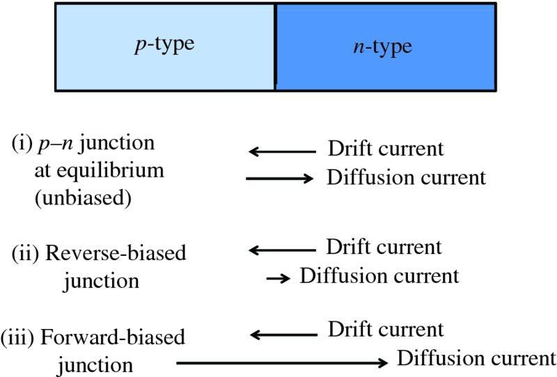
Figure 5.16 A summary of the currents that flow across a p–n junction for: (i) p–n junction in equilibrium, (ii) reverse-biased junction and (iii) forward-biased junction. The drift current is relatively insensitive to bias voltage and is essentially the same for all three conditions. At equilibrium, when there is no bias, the diffusion and drift currents are equal and opposite. When the p–n junction is reverse-biased, the diffusion current is essentially zero. When the p–n junction is forward-biased, the diffusion current is much greater than the drift current.
We can make an analogy between a p–n junction, with its two layers of charge on either side of the junction, and a pair of parallel conducting plates with a voltage difference between them. These plates form an electrical capacitor with a layer of positive charge on one plate and a layer of negative charge on the other. Similarly, the p–n junction can also be viewed as a capacitor. As the bias voltage changes, the two layers of charge at the p–n junction vary in width and therefore in the amount of charge they contain. Thus the capacitance of the junction can be controlled by the bias voltage. This effect is exploited in a device called the varactor diode, which finds application, for example, as the tuning capacitor in a radio receiver.
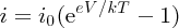
5.3.3 The current–voltage characteristic of a p–n junction
The net current i flowing across a p–n junction is the combination of the diffusion and drift currents: i = idiff − idrift. We have seen (i) that no net current flows across a p–n junction when the voltage V applied across it is zero; (ii) that current does flow when the junction is forward-biased (V positive) and this current increases rapidly with increasing forward bias voltage; and (iii) that a small but finite current flows across the junction in the opposite direction when the junction is reverse-biased (V negative) and that this current is essentially independent of the value of the bias voltage. This dependence of the current on bias voltage results in the i–V curve shown in Figure 5.17, which is a plot of i against V. As V increases in the forward direction, i increases rapidly, but when V is increased in the reverse direction, i remains constant. The reverse-bias current is called the reverse saturation current i0 and is just the drift current idrift. Its magnitude has been exaggerated in Figure 5.17 for the sake of clarity and for a silicon p–n junction, i0 typically lies within in the range 10− 10–10− 12 A. The dependence of current i on bias voltage V is described by the equation
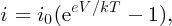
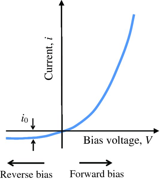
Figure 5.17 The current–voltage characteristic of a p–n junction, where V is the applied voltage and i is the current flowing through the junction. As the voltage V is increased in the forward direction, corresponding to forward bias, the current i increases rapidly. However, when the voltage V is increased in the reverse direction, corresponding to reverse bias, the reverse saturation current i0 remains essentially constant. The magnitude of i0 is exaggerated for the sake of clarity.
where T is the absolute temperature and k is the Boltzmann constant. Obviously the non-linear form of this equation is quite different from the linear form of Ohm's law, i = V/R.
It is apparent from Figure 5.17 that a p–n junction essentially allows current to flow in only one direction, apart from the extremely small reverse saturation current. Hence, a p–n junction is a rectifying device called a diode. Consequently, Equation (5.5), which describes the current–voltage characteristic of a p–n junction, is also known as the diode equation. A diode has many important applications. For example, it can be used to convert an alternating current (AC) voltage into a direct current (DC) voltage.
We can use our model of a p–n junction with its potential barrier to arrive at Equation (5.5). For this we need to consider the probability that a majority carrier, electron or hole, can surmount the internal potential barrier of a p–n junction. When a large number of particles is in thermal equilibrium, there is a continual exchange of energy between the particles. At any instant, the energy of an individual particle is not known; it may be larger or smaller than the average. However, there is a well-defined probability distribution for the whole assembly of particles called the Boltzmann distribution. It gives the probability of a particle having energy E at temperature T. The Boltzmann distribution is expressed in the form
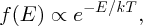
where T is temperature, k is the Boltzmann constant and the factor e− E/kT is called the Boltzmann factor. The precise form of the distribution depends on the system under consideration, but the temperature dependence of the distribution is always governed by a Boltzmann factor. This factor may be multiplied by other energy-dependent terms, but these do not include the temperature. The Boltzmann distribution applies to quantum systems as in the present context but also to classical systems, as in the following example.
In the case of a p–n junction in equilibrium, the internal barrier of height V0 inhibits the majority charge carriers diffusing across the junction. According to
the Boltzmann distribution, the probability of a charge carrier at temperature T having energy eV0 is proportional to
 . It follows that the probability that a charge carrier can surmount the barrier and
contribute to the diffusion current is also proportional to
. It follows that the probability that a charge carrier can surmount the barrier and
contribute to the diffusion current is also proportional to
 . In the case of the forward-biased p–n junction, the barrier is lowered from V0 to (V0 − V). Then the probability that a majority charge carrier has enough energy to surmount
this barrier of reduced height is proportional to
. In the case of the forward-biased p–n junction, the barrier is lowered from V0 to (V0 − V). Then the probability that a majority charge carrier has enough energy to surmount
this barrier of reduced height is proportional to
 . The fractional increase in the probability is
The diffusion current, which is proportional to the number of majority carriers surmounting the barrier, increases by the same factor and so

The net current i flowing through the junction is then

where we have used the fact that idrift is equal to the reverse saturation current i0. When the junction is at equilibrium, V = 0 and i = 0 with eeV/kT = 1. Hence, the constant is equal to i0 and i = i0(eeV/kT − 1) in agreement with Equation (5.5).
5.3.4 Electron and hole concentrations in a semiconductor
In Section 5.2.1 we described the energy bands in a semiconductor and how the atomic electrons fill the available energy levels, starting with the lowest energy band. In order to describe the resulting electron (and hole) densities or concentrations in these energy bands, we need to know the following:
- the density of states in the bands;
- the probability of each of these states being occupied.
The first factor is given by the density of states function, Z(E), which may be defined as the number of energy states per unit energy per unit volume. We encountered an analogous function in Section 4.2.3 for the density of standing electromagnetic waves in a blackbody cavity. The form of Z(E) can be obtained in a similar fashion, where geometrical arguments are used to count the number of quantum states that are contained in a given energy range (see Hook and Hall,1 Section 5.3 for further details). For the conduction band, the function Z(E) is given by
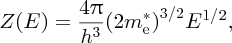
where h is Planck's constant, the energy E is measured from the bottom of the conduction band, and me is the effective mass of the electrons. The form of Z(E) is given in Figure 5.18, which shows its parabolic dependence on energy.
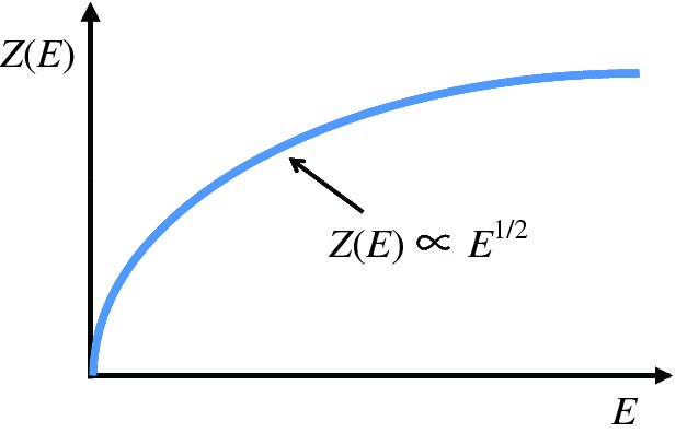
Figure 5.18 The density of states function Z(E) for electrons in the conduction band of a semiconductor.
The second factor depends on the fact that electrons are fermions and obey the Pauli exclusion principle. For fermions, the probability of a particular level at energy E being occupied is given by the Fermi–Dirac distribution:
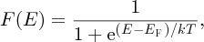
where T is the absolute temperature and EF is a characteristic energy called the Fermi energy. We plot this important function in Figure 5.19. At T = 0, F(E) is unity for energies less than EF and zero for energies greater than EF. At temperatures above absolute zero the distribution changes as also shown in Figure 5.19. Notice that at any finite temperature, the probability of occupation of an energy level at E = EF is 0.5 and indeed we can use this fact to define the Fermi energy. The symmetry of the Fermi–Dirac distribution about the Fermi energy makes this energy a natural reference point.
Figure 5.19 The Fermi–Dirac distribution F(E), which gives the probability of a particular state at energy E being occupied by an electron, which is a fermion. The distribution is shown for T = 0 K and for increasing temperatures. At any finite temperature, the probability of occupation of an energy level at E = EF is 0.5, where EF is defined as the Fermi energy.
If (E−EF) ≫ kT, Equation (5.9) reduces to
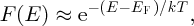
which has the same form as the Boltzmann distribution (Equation 5.6). For electrons in the conduction band of a semiconductor, the energy difference (E − EF) is typically ∼0.5 eV while the value of kT at room temperature is approximately 1/40 eV and so this approximation is usually valid. In that case, Equation (5.10) gives us further physical meaning to the Fermi energy. We can use Equation (5.10) just as we would use the Boltzmann distribution, so long as we take the electron to have originated in an energy level corresponding to the Fermi energy. We emphasise, however, that this Fermi level, which occurs at the Fermi energy, is not a physical energy level that a particle occupies; rather it is a hypothetical energy level that lies at that energy. In a semiconductor, the Fermi energy lies somewhere between the top of the valence band and the bottom of the conduction band. In particular, the Fermi energy in an intrinsic semiconductor lies in the middle of the energy gap.
We will use the case of an intrinsic semiconductor to illustrate graphically the resulting concentrations of electrons in the conduction band and holes in the valence band. Figure 5.20(a) shows the density of state function Z(E) for the conduction and valence bands. In the conduction band, Z(E) increases with increasing energy from the bottom of the band. In the valence band, Z(E) has mirror symmetry with respect to Z(E) in the conduction band and decreases as it approaches the top of the band. Figure 5.20(b) shows the Fermi–Dirac distribution. For the case of an intrinsic semiconductor, the Fermi energy is centred on the middle of the band gap. At finite temperatures this Fermi–Dirac distribution has tails that extend into the valence and conduction bands, as shown.
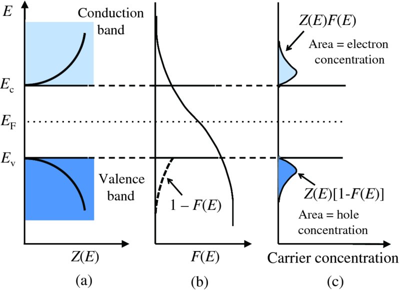
Figure 5.20 (a) The density of state functions Z(E) for the conduction and valence bands of a semiconductor. (b) The Fermi–Dirac distribution in an intrinsic semiconductor, in which the Fermi energy is centred on the middle of the band gap. At finite temperatures this Fermi–Dirac distribution has tails that extend into the valence and conduction bands. (c) The concentration of electrons in the conduction band is obtained by summing the product Z(E)F(E), and is equal to the shaded area as indicated. The concentration of holes in the valence bans is obtained by summing the product Z(E)[1 – F(E)] and is equal to the other shaded area, as indicated. The two shaded areas are the same, reflecting the fact that the number of electrons in the conduction band is equal to the number of holes in the valence band in an intrinsic semiconductor.
The concentration of electrons in the conduction band is obtained by summing the product Z(E)F(E) of the density of states function and the Fermi–Dirac distribution over the energy range of interest. This product is shown in Figure 5.20(c) and the concentration of electrons is equal to the shaded area indicated in the figure. If the probability of finding an electron with energy E is F(E), the probability of not finding an electron at that energy is [1 − F(E)], which is the probability of finding a hole. Thus the concentration of holes in the valence band is obtained by summing the product Z(E)[1 − F(E)], which is also shown in Figure 5.20(c). The hole concentration is again given by the shaded area indicated in the figure. We expect the two shaded areas to be the same, reflecting the fact that the number of electrons in the conduction band is equal to the number of holes in the valence band in an intrinsic semiconductor. This follows naturally from the symmetry of the density of state function in the two bands and the symmetry of the Fermi–Dirac distribution when the Fermi energy is placed at the middle of the gap. If the Fermi energy were placed at any other energy in the gap, the areas would not be equal. Figure 5.20 shows the situation for an intrinsic semiconductor, but the concentration of charge carriers in any semiconductor, intrinsic or extrinsic, is given by the product of the density of states function and the Fermi–Dirac distribution. We simply need to take the appropriate Fermi energy for the semiconductor.
For the concentration n of electrons in the conduction band, we can write
where Z(E) and F(E) are given by Equations (5.8) and (5.9), respectively. Evaluation of the integral gives
where
and Ec is defined in Figure 5.20. We may think of Nc as a normalisation factor, which describes the total number of electrons that are promoted to the conduction band. In a similar way, to determine the concentration, p, of holes in the valence band, we evaluate the integral
which gives
where again, Nv is a constant of normalisation and is given by

and Ev is again defined by Figure 5.20. m*h is the effective mass of the holes, which we have taken to be the same as the effective mass of the electrons. The product of the electron and hole concentrations is given by

since Eg = Ec − Ev. We see that the product of n and p is fixed at constant temperature. Although we have seen it here for the case of an intrinsic semiconductor, Equation (5.18) also applies to extrinsic semiconductors. It is known as the law of mass action for semiconductors. It is a very important relationship as, once we know n or p, we can determine the other. Thus, if we dope an intrinsic semiconductor with acceptor atoms to increase the concentration of holes, the concentration of electrons must decrease accordingly. For the particular case of an intrinsic semiconductor, n = p = ni, where ni is the intrinsic carrier concentration. Hence

We see that the temperature variation of ni is exponential. i.e.
 . Moreover, the product of electron and hole concentrations in any semiconductor can
conveniently be written
. Moreover, the product of electron and hole concentrations in any semiconductor can
conveniently be written

5.3.5 The Fermi energy in a p–n junction
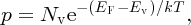
In an n-type semiconductor, the electron concentration in the conduction band is high, with the result that the Fermi energy lies just below the bottom of the conduction band. This is illustrated in Figure 5.21(b). On the other hand, in a p-type semiconductor, the hole concentration in the valence band is high, with the result that the Fermi energy lies just above the bottom of the valence band, as illustrated in Figure 5.21(a). When, however, we have a junction between a p-type semiconductor and an n-type semiconductor, the Fermi energy must be at a constant level throughout the semiconductor, as shown in Figure 5.22. With this condition, the energy of the system is minimised. We can make an analogy here with temperature in a system consisting of several parts. We know that at equilibrium the temperature must be the same throughout the system. Indeed, both temperature and the Fermi energy, more generally called the chemical potential, are thermodynamic quantities.
Figure 5.21 (a) The Fermi energy in a p-type semiconductor lies just above the top of the valence band. (b) In an n-type semiconductor, the Fermi energy lies just below the bottom of the conduction band.
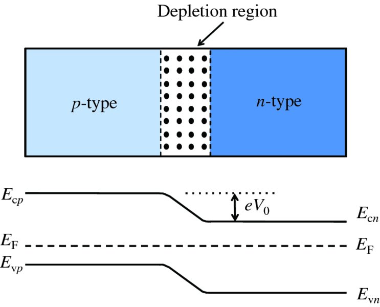
Figure 5.22 The energy levels in an unbiased p–n junction. Note that the Fermi energy is constant throughout the semiconductor. There is a step change, eV0, in energy between the n and p regions. This inhibits electrons from the n region diffusing into the p region. Similarly, holes are inhibited from diffusing into the n region.
If the p and n regions are made from the same semiconductor, the band gap Eg is the same for both regions. Then, as we can see from Figure 5.22, the requirement for a constant Fermi energy means that the energy levels in the n-type are lowered with respect to those in the p-type. The amount by which they are lowered is eV0, where V0 is just the contact potential that we encountered previously. The step in energy inhibits electrons from the n-type diffusing into the p-type, and holes in the p-type are inhibited from diffusing into the n-type, as we also saw in Section 5.3.1. We can change this equilibrium situation by forward-biasing the p–n junction, i.e. by applying a positive voltage, V, to the p-type with respect to the n-type, as shown in Figure 5.23. This raises the energy levels in the n-type relative to the p-type, decreasing the energy difference between them by an amount eV. It then becomes easier for the electrons in the n region to diffuse into the p region and for the holes in the p region to diffuse into the n region. This increases the diffusion current by the Boltzmann factor eeV/kT. It is important to note, however, that in a biased p–n junction the Fermi level is no longer constant throughout the composite semiconductor : the Fermi levels on the two sides are displaced by the magnitude of the bias voltage. When the p–n junction is reverse-biased, as in Figure 5.24, the energy levels in the n-type are lowered relative to the p-type. Then the electrons from the n-type and the holes from the p-type have an even higher barrier to climb and relatively few majority carriers diffuse across the junction. Again, the Fermi level is no longer constant throughout the semiconductor.
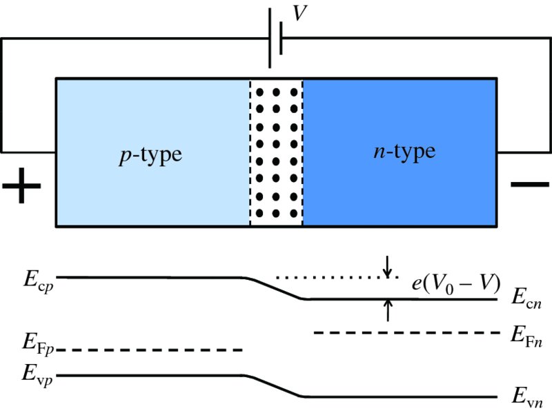
Figure 5.23 The energy levels in a forward-biased p–n junction. The energy bands in the n-type are raised relative to the bands in the p-type, decreasing the energy difference between them by eV. It then becomes easier for the electrons in the n region to diffuse into the p region and for the holes in the p region to diffuse into the n region. The Fermi level is no longer constant throughout the semiconductor; the Fermi levels on the two sides are displaced by the magnitude of the bias voltage V.
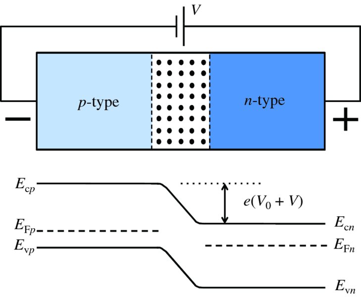
Figure 5.24 The energy levels in a reverse-biased p–n junction. The energy bands in the n-type are lowered relative to the p-type. Electrons from the n region and holes from the p region have an even higher barrier to climb and relatively few of these majority carriers diffuse across the junction. Again, the Fermi level is no longer constant throughout the semiconductor.
5.4 Semiconductor solar cells
A semiconductor solar cell is essentially a p–n junction, although one that has a large surface area to collect solar radiation. In this section, we describe what happens when sunlight is incident on a p–n junction and how the electrical power that it delivers to an external load can be maximised. We also describe some ways of increasing the efficiency of solar cells and the use of alternative solar cell materials.
5.4.1 Photon absorption at a p–n junction
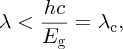
When a photon is incident upon a semiconductor such as silicon, an electron may be promoted from the valence to the conduction band if the photon has an energy hν that is greater than the band gap Eg, i.e.

or in terms of wavelength λ:
where λc is the critical wavelength for the semiconductor. For silicon, Eg = 1.11 eV and λc = 1.12 μm. This process produces an electron–hole pair as illustrated in Figure 5.25. Subsequently, the generated electrons and holes recombine with charge carriers of opposite sign. Suppose now that a photon is incident upon the depletion layer of a p–n junction. Again the photon may produce an electron–hole pair, as illustrated in Figure 5.26. But now the inbuilt electric field across the junction causes the electron and hole to separate and drift across the depletion layer. The electrons move into the n region and the holes move into the p region. In terms of the energy level diagram shown in Figure 5.26, an electron is promoted to the conduction band and a hole is left in the valence band. The promoted electron then ‘rolls down the hill’ into the n region, as the conduction band of the n-type lies energetically below the conduction band of the p-type. Similarly the holes, of opposite charge, move into the valence band of the p-type, which is at a lower energy for them. This movement of electrons and holes across the junction results in a flow of electron current in an external circuit; electrons flow from the n-type around the external circuit and enter the p-type where they recombine with holes. Electron–hole pairs that are generated within a diffusion length or so of the depletion layer may also contribute to the flow of charge carriers across the junction.
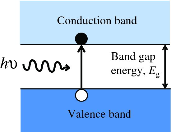
Figure 5.25 When a photon is incident upon a semiconductor material, an electron may be promoted from the valence band to the conduction band if the photon has an energy hν that is greater than the band gap Eg.
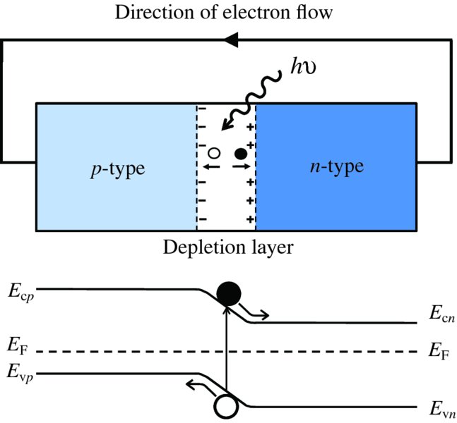
Figure 5.26 When a photon is incident upon the depletion region of a p–n junction, the photon may produce an electron–hole pair. The inbuilt electric field across the junction causes the electron and hole to separate and drift across the depletion layer. The electron moves into the n region and the hole moves into the p region. In terms of the energy level diagram shown, an electron is promoted to the conduction band and a hole is left in the valence band. The promoted electron then ‘rolls down the hill’ into the n-type, as the conduction band of the n-type lies energetically below the conduction band of the p-type. Similarly, the holes, of opposite charge, move into the valence band of the p-type, which is at a lower energy for them. This movement of electrons and holes across the junction results in a flow of electron current in an external circuit; electrons flow from the n region around the external circuit and enter the p region where they recombine with holes. Electron–hole pairs that are generated within a diffusion length or so of the depletion layer may also contribute to the flow of charge carriers across the junction.
Equation (5.2) follows from the conservation of energy. As in any physical reaction, the total momentum of the system must also be conserved. For some semiconductors called direct band semiconductors, this happens naturally. Gallium arsenide (GaAs) is an example of a direct band semiconductor. Some semiconductors, however, require a third body to be involved in the reaction to conserve momentum. These are called indirect band semiconductors. Silicon (Si), which is the most widely used semiconductor in solar cells, is an example of an indirect band semiconductor. The third body involved is an atom in the crystal lattice of the semiconductor, which absorbs the momentum and becomes vibrationally excited in the process. Such a vibration is called a phonon. Importantly, whenever a reaction requires three bodies to be involved, that reaction is less likely to occur than one in which just two bodies are involved.
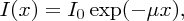
The difference between direct and indirect band gap semiconductors shows up in their absorption coefficients for solar radiation. In Section 3.2.3 we considered the attenuation of a beam of particles as they pass through an absorbing medium and we found that the flux of the beam reduces exponentially with distance travelled in the medium. Similarly, when light passes through a medium, its irradiance I reduces exponentially with distance x according to
where μ is the absorption coefficient and I0 is the initial irradiance. The absorption coefficients for Si and GaAs are plotted against photon energy in Figure 5.27. Each of the curves shows a sharp onset at their respective critical wavelengths, corresponding to their band gap energies; photons of energy less than the band gap of a semiconductor are transmitted with zero or very little absorption. We see that the attenuation coefficient is much lower for the indirect band gap semiconductor Si than the direct band gap semiconductor GaAs over most of the solar wavelength range; the values of μ for Si are ∼103/cm and ∼105/cm for GaAs. Consequently, a solar cell using Si as the semiconductor has a slice of Si crystal that is ∼300 μm thick, while a solar cell using GaAs can use a much thinner crystal.
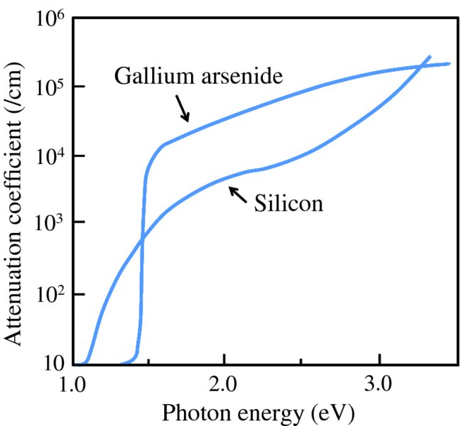
Figure 5.27 The attenuation coefficient curves for silicon (Si) and gallium arsenide (GaAs) as a function of photon energy. Each of the curves shows a sharp onset at the respective band gap energies: 1.11 eV for Si and 1.43 eV for GaAs. Photons of energy less than the band gap of a semiconductor are transmitted with zero or very little absorption. The attenuation coefficient is much lower for the indirect band gap semiconductor Si than the direct band gap semiconductor GaAs over most of the solar wavelength range.
5.4.2 Power generation by a solar cell
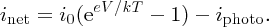
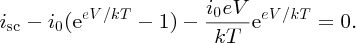
As we have described, sunlight that is incident on a solar cell generates electron–hole pairs and these charged carriers drift across the p–n junction to give rise to a photoelectric current that flows through an external circuit. Suppose that the p and n regions of an illuminated solar cell are connected directly together as in Figure 5.28(a). In this case the current flowing in the external circuit is called the short-circuit current, isc. In this figure the arrow points in the direction of conventional current flow, (see also Figure 5.29 caption). If, on the other hand, the external circuit is open, as in Figure 5.28(b), the current flowing in the circuit will be zero. In the latter case, the movement of charge carriers across the junction results in an accumulation of charge in both the n and p regions; the p region becomes positively charged and the n region becomes negatively charged. This generates a voltage difference, V, between the two regions and, as the p region is at a positive potential with respect to the n region, the p–n junction becomes forward-biased (see Figure 5.15). This reduces the width of the depletion layer so that the diffusion current increases. This continues until V increases to the point where the diffusion current exactly balances the net drift current flowing in the opposite direction. The net drift current is now due to electron–hole pairs that are generated thermally plus those that are generated by the photons incident on the solar cell. The potential difference between the p and n regions when they are not connected externally is called the open circuit voltage, Voc.
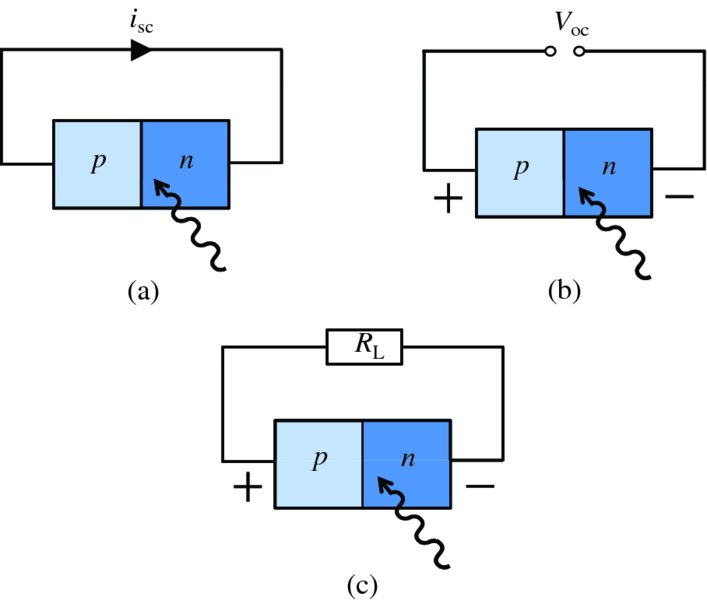
Figure 5.28 (a) A solar cell in the short-circuit mode with short-circuit current isc. (b) A solar cell in the open-circuit mode with open-circuit voltage Voc. (c) A solar cell connected to a load of finite resistance RL. The current flowing through the load is less than ioc and the voltage across the load is less than Voc.
More generally, an electrical load such as an electrical resistance RL is connected across a solar cell, as shown in Figure 5.28(c). Incident sunlight generates a voltage difference between the p and n regions and a photoelectric current flows in the external circuit. Electrical power is thus delivered to the load. In this case, however, the voltage across the load and the delivered current will be less than the open circuit voltage Voc and the short circuit current isc, respectively, as we shall see in Section 5.4.3.
Solar cell equation
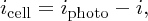
In our discussions of the p–n junction in Section 5.3, we encountered: (i) the drift current idrift due to minority charge carriers that are thermally generated and which drift across the junction under the influence of the junction field; and (ii) the diffusion current idiff due to the diffusion of majority charge carriers across the junction, which flows in the opposite direction to the drift current. Now for an illuminated p–n junction, we also have a photocurrent iphoto due to the electron–hole pairs generated by the incident photons. These photon-induced electrons and holes are affected by the junction field in the same way as the electrons and holes that are thermally generated. Thus, the photocurrent flows in the same direction as the drift current and hence the net current inet flowing across the junction is given by

Following Section 5.3.3, we take idiff = i0eeV/kT, where now V is the voltage induced across the p–n junction by the incident sunlight, and idrift = i0. This gives
In this expression, as iphoto increases the magnitude of inet also increases, but inet becomes more negative. A solar cell is conventionally considered to be a battery that delivers a current icell to an external load that becomes more positive as iphoto increases, as illustrated in Figure 5.29. Hence it is convenient to define icell as icell = −inet so that
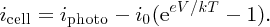
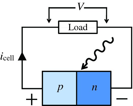
Figure 5.29 A solar cell is conventionally considered to be a battery that delivers a positive current icell to an external load. V is the voltage output of the cell.
where V is now the voltage output of the solar cell and both icell and V are positive quantities. A plot of solar cell current icell against cell voltage V is shown as the solid curve in Figure 5.30. The shaded area is the quadrant in which the cell generates electrical power. The figure also illustrates what happens as the illumination of the cell increases; the icell–V curve moves upward as indicated by the dashed curves. As more current is drawn from the cell, the cell voltage steadily falls, following the solid curve on Figure 5.30.
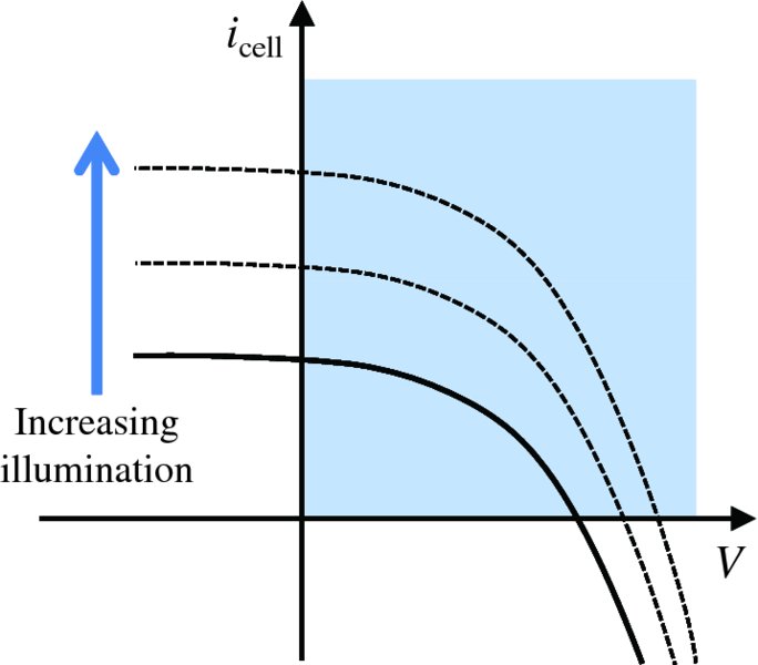
Figure 5.30 The solid curve is a plot of the output current icell of a solar cell against its output voltage V. The shaded area of the graph is the quadrant in which the cell generates electrical power. The figure also indicates how the icell–V curve moves upward as the illumination of the cell is increased, as shown by the dashed curves.
We can understand the behaviour of the solar cell voltage in the following way. We recognise the second term in Equation (5.24) from the diode equation:
(see Section 5.3.3). Hence we write Equation (5.24) as
and we can represent a solar cell by the equivalent circuit shown in Figure 5.31. The cell is represented by a current source, delivering current iphoto, and this current source is connected in parallel with a diode and with the load. The diode represents the p–n junction of the cell and the voltage across it is the cell voltage V. The arrowheads indicating the direction of current flow point in the direction of conventional current flow. For a given illumination, iphoto is fixed. If the load draws more current, i.e. icell increases, then i must reduce. Then the voltage V must also decrease according to Equation (5.5), giving the shape of the solid icell–V curve shown in Figure 5.30.
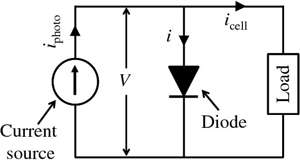
Figure 5.31 A solar cell can be represented by a current source, delivering current iphoto, that is connected in parallel with a diode and with the load. The diode represents the p–n junction of the cell. For a given illumination, iphoto is fixed. As the load draws more current, i.e. icell increases, the current, i, flowing through the diode must decrease according to icell = iphoto − i and this also reduces the voltage V in accordance with the diode equation, i = i0(eeV/kT − 1).
When the p and n regions of a solar cell are connected together as in Figure 5.28(a), the cell voltage V must be zero and the current flowing between the two regions is the short-circuit current isc. In addition, according to Equation (5.24), with V = 0, the cell current flowing in the external circuit is iphoto. Hence we take isc = iphoto, which says that the short-circuit current is equal to the photocurrent produced by the incident sunlight. Substituting for iphoto = isc in Equation (5.24) we obtain
This is the solar cell equation.
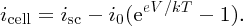
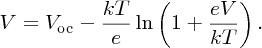
5.4.3 Maximum power delivery from a solar cell
When the solar cell is left open circuit, as shown in Figure 5.28(b), the output voltage is the open-circuit voltage Voc. In this case, icell = 0. Then, rearranging Equation (5.26), we obtain
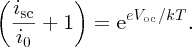
Usually, isc ≫ i0 and so
In practice, the value of Voc ∼0.7 eV.
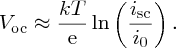
For a load of finite resistance RL, as in Figure 5.28(c), the current flowing through the load will be less than isc and the voltage across the load will be less than Voc. Of course, we would like to deliver as much power to the load as possible and we can achieve this by suitably adjusting the value of RL. The values of current and voltage that together provide the maximum power are called imp and Vmp, respectively. We can deduce expressions for imp and Vmp as follows. The power P delivered by the solar cell is equal to the product of the cell current icell and the cell voltage V. Substituting for icell from Equation (5.26) we have

To find Vmp, we differentiate this equation with respect to V and set dP/dV = 0. This gives
In general, eV/kT ≫ 1, and we can write
Substituting for
 from Equation (5.27), we obtain
Rearranging this equation gives
The value of V given by Equation (5.30) is just Vmp:
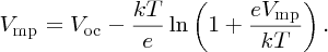
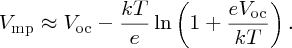
To make this result more tractable, we note that in practice Vmp ≈ Voc and, in addition, any logarithmic function ln [f(x)] varies only slowly with x. Hence we substitute Voc for Vmp in the logarithmic term to give our final result for Vmp:
In a similar fashion, we find that the current for maximum power is given by
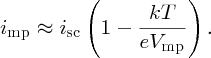
For strong illumination, kT/eVmp ≪ 1, in which case imp ≈ isc. Also under this condition, the second term in Equation (5.32) for Vmp is small compared with Voc and hence Vmp ≈ Voc.
The above results are presented graphically in Figure 5.32(a), which shows the icell –V curve for a solar cell in the power generation quadrant. For V = 0 (closed circuit), icell = isc, and the output power P is zero, as we see in Figure 5.32(b). For V = Voc (open circuit), icell = 0 and P is also zero. Maximum power, Pmp, occurs for V = Vmp and icell = imp and is given by the area of the shaded rectangle in Figure 5.32(a). The figure also illustrates that, in practice, Vmp ≈ Voc, and imp ≈ isc. The ratio of the maximum power Pmp and the product iscVoc is called the fill factor, FF:
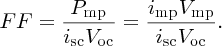
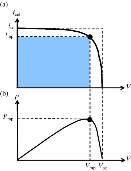
Figure 5.32 (a) The icell–V curve for a solar cell in the power generation quadrant. Maximum power Pmp occurs for V = Vmp, icell = imp and is given by the area of the shaded rectangle. The figure also illustrates that, in practice, Vmp ≈ Voc, and imp ≈ isc. The ratio of the maximum power, Pmp, and the product, iscVoc, is the fill factor. (b) For V = 0 (closed circuit), icell = isc, and the output power P is zero. For V = Voc (open circuit), icell = 0 and P is also zero.
The area corresponding to iscVoc is also indicated in Figure 5.32(a). In practice, fill factors are ∼80%.
Perhaps the most useful figure of merit for a solar cell is its power conversion efficiency η, which is defined as the ratio of the maximum electrical power Pmp to the incident solar power PS:
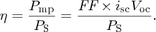
By convention, solar cell efficiencies are measured under standard test conditions. These are an incidence irradiance of 1000 W/m2 with an AM1.5 air mass spectrum to simulate atmospheric absorption. For commercial solar cells, η ∼ 20%.
5.4.4 The Shockley–Queisser limit
We saw in Chapter 4 that the Sun can be considered to be a blackbody at a temperature of ∼5800 K and that the solar spectrum contains a continuous range of photon wavelengths. We will now see that not all the sunlight incident on a solar cell can be converted into electrical power. In 1961, William Shockley and Hans Queisser made a detailed analysis of the p–n junction to determine the maximum possible efficiency of a semiconductor solar cell; the efficiency of converting solar power into electrical power. The important result of their theoretical considerations is that the maximum possible efficiency of a solar cell is about 34%, when atmospheric absorption is taken into account. So for example, if the solar irradiance is 1000 W/m2, the maximum electrical power that can be obtained is 340 W/m2 of the solar cell. The analysis of Shockley and Queisser is based on several factors. These include: (i) not all solar photons have enough energy to promote an electron to the conduction band of the semiconductor material; (ii) a fraction of the photon energy is dissipated as heat in the crystal lattice; and (iii) a fraction of the photon-generated electrons and holes recombine before they can contribute to the photocurrent.
Dissipation of energy in the crystal lattice
To illustrate this effect, we consider, as Shockley and Queisser did, a blackbody spectrum for a temperature of 5800 K to represent the solar spectrum. This is shown in Figure 5.33, which plots spectral irradiance against wavelength. The total area under the curve gives the total power in the spectrum. Also indicated in the figure is the critical wavelength for silicon, i.e. the maximum wavelength that can promote an electron into the conduction band. The figure shows three different regions of the ‘solar’ spectrum, A, B and C. Photons lying in region A do not have enough energy to cause promotion of an electron across the band gap, i.e. hc/λ < Eg, and so they do not produce any electrical power; they may simply heat the crystal lattice. For photon energies greater than the band gap, i.e. hc/λ > Eg, the excited electron goes into an energy level that lies above the bottom of the conduction band, as shown in Figure 5.34. This electron very quickly drops down to the bottom of the conduction band and its excess energy (hc/λ − Eg) is dissipated as heat in the crystal lattice. The greater the energy of the photon, the greater is the fraction of its energy that is lost as heat. The area of region C in Figure 5.33 represents the power that is dissipated in this way. Thus the area of region B in the figure represents the only solar power that can, in principle, be obtained from a solar cell. The relative size of the area of region B depends on the value of the semiconductor band gap. For the case of silicon, the area of region B compared with the total area of the spectrum is about 45%. If a semiconductor with a larger band gap is chosen, fewer photons at the infrared end of the solar spectrum are able to promote electrons across the band gap, but visible photons will do so more efficiently; less of their energy will be lost as heat to the lattice. On the other hand, if the band gap is made smaller, more photons at the infrared end of the solar spectrum are able to promote electrons but visible photons will do so less efficiently. This correctly suggests that there is an optimum band gap for maximum solar cell efficiency, as we shall see.
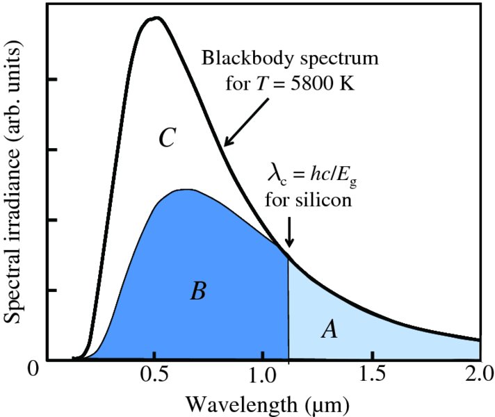
Figure 5.33 A blackbody spectrum for a temperature of 5800 K. Also indicated is the critical wavelength (1.12 μm) for silicon. Photons lying in region A do not have enough energy to cause promotion of an electron across the band gap. For photon energies greater than the band gap, a fraction of their energy is dissipated as heat in the crystal lattice. The area of region C represents the power that is lost in this way. The area of region B represents the only part of the solar power that can, in principle, be obtained from a solar cell. The area of region B compared with the total area under the blackbody curve is about 45%.
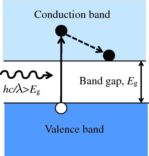
Figure 5.34 For photon energies greater than the band gap, the excited electron goes into an energy level that lies above the bottom of the conduction band. This electron very quickly drops down to the bottom of the conduction band and its excess energy (hc/λ − Eg) is dissipated as heat in the crystal lattice.
Electron–hole recombination
Electrons and holes that are generated by incident photons have a tendency to recombine with charge carriers of opposite sign. If recombination occurs before the electron–hole pair can contribute to the photocurrent, the efficiency of the cell is reduced. The fundamental recombination process is radiative recombination. This process is illustrated in Figure 5.35. An electron recombines with a hole and the result is that a photon is emitted with energy roughly equal to the band gap. Shockley and Queisser took account of radiative recombination using a detailed-balance principle, based on thermodynamic considerations. This principle essentially says that when the solar cell is not illuminated, but is in thermodynamic equilibrium with its surroundings, the rate of generation of electron–hole pairs must be equal to the recombination rate. Then when the cell is illuminated by sunlight, the rate of electron–hole pair generation is equal to the rate of radiative recombination plus the rate at which electrons are consumed in the delivery of current to the external load. Using the detailed balance principle, Shockley and Queisser deduced that radiative recombination reduces solar cell efficiency by about 10%.
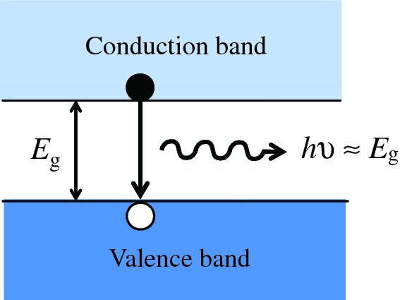
Figure 5.35 The process of radiative recombination. An electron recombines with a hole and the result is that a photon is emitted with an energy that is roughly equal to the band gap.
From their theoretical treatment of the p–n junction, Shockley and Queisser obtained a curve for solar cell efficiency as a function of band gap energy. The form of this curve when atmospheric effects are taken into account is shown in Figure 5.36. The maximum efficiency is 34% and this is achieved for a band gap of 1.34 eV. Silicon has a band gap that is reasonably close to this optimum value, and for its band gap of 1.11 eV the efficiency is 29%. The efficiency of modern commercial silicon solar cells is about 22%. The difference is partly due to practical effects such as reflection of light from the front surface of the cell and light blockage from the thin connecting wires on its surface. And in practical cells, not all of the available charge carriers are collected by the electric field of the junction. An efficiency of 22% may seem modest but we recall that the efficiency of say a petrol engine has a similar value. The Shockley and Queisser limit applies to a single p–n junction. We will see in Section 5.4.6 that the limit can be circumvented by using in tandem two or more p–n junctions that have different band gaps.
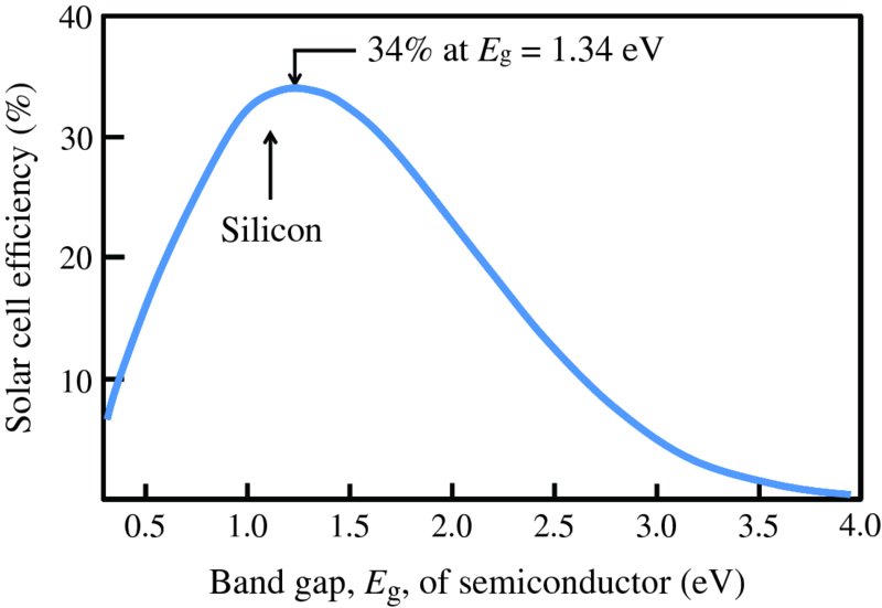
Figure 5.36 The efficiency of a solar cell as a function of band gap energy, Eg, when the cell is illuminated by solar radiation and atmospheric effects are taken into account. This curve is deduced from the theoretical considerations of Shockley and Queisser. The maximum efficiency is 34% and this is achieved for a band gap of 1.34 eV.
5.4.5 Solar cell construction
The first practical solar cells used crystalline silicon as the semiconductor material and the majority of solar cells still use this material. Use of silicon as the semiconductor material has a number of advantages: silicon is one of the most abundant elements on Earth; its band gap is close to being ideally matched to the solar spectrum; it is chemically stable; and it is non-toxic. And because of the microelectronics industry, the production and processing of extremely pure crystalline silicon are well developed. The disadvantage of silicon is that it has a relatively low attenuation coefficient for solar radiation because it is an indirect band gap semiconductor (see Section 5.4.1).
Figure 5.37 illustrates the construction of a typical solar cell based on a single crystal of silicon. A p–n junction is formed within the silicon crystal by diffusion of the appropriate impurities into the crystal. It is favourable to have the thickness (∼1 μm) of the n-type region much less than the thickness (∼300 μm) of the p-type region, but for the n-type to be more heavily doped. This allows most of the absorption of light to occur in the p region. The diffusion length of the charge carriers in the p region is ∼100 μm and, as noted previously, charge carriers produced within this length may migrate to the junction and contribute to the photocurrent. A grid of wires is placed between an anti-reflectance coating and the semiconductor surface to provide electrical contact to the cell. Semiconductor materials have relatively high values of electrical resistivity and the grid is arranged to minimise resistance losses in the surface of the material. There is also an electrode at the back of the cell to complete the electrical circuit. Typically, a cell may be ∼10 cm × 10 cm in size and a number of these individual cells can be connected to form a module. For example, typically 36 cells are connected in series to provide an overvoltage to charge 12 V batteries. Under clear sky conditions, the output current of the cell is ∼300 A/m2.
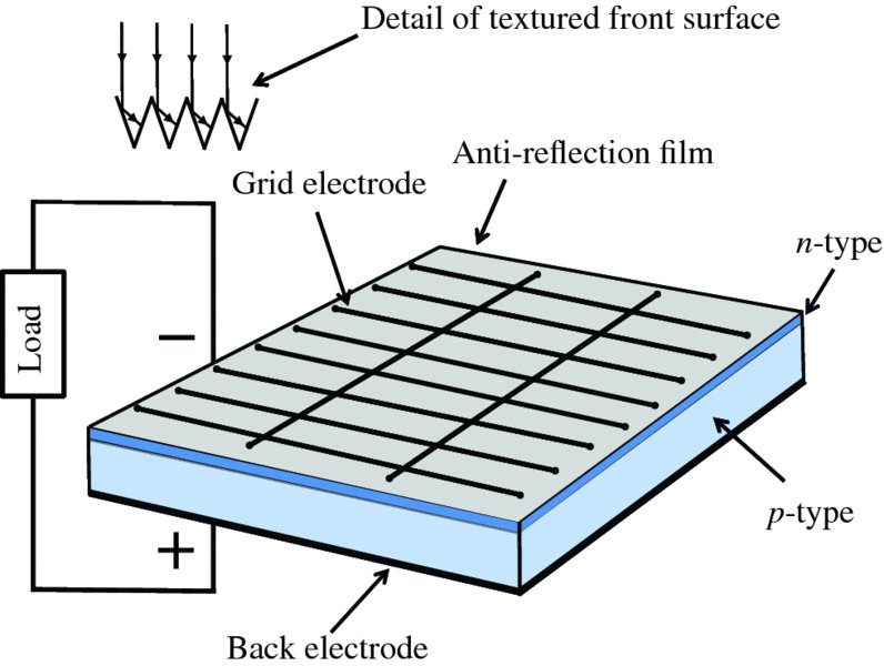
Figure 5.37 The construction of a typical solar cell. The solar cell is based on a thin single crystal of silicon, the kind used in microelectronic devices. A p–n junction is formed within the silicon layer. The thickness (∼1 μm) of the n-type region is much less than the thickness (∼300 μm) of the p-type region, but the n-type is more heavily doped. This allows most of the absorption of light to occur in the p region. Typically a cell may be ∼10 cm × 10 cm in size. A grid of wires is placed between an anti-reflectance coating and the semiconductor surface to provide electrical contact to the cell. There is also an electrode at the back of the cell to complete the circuit. Light collection can be enhanced by texturing the front surface of the solar cell by a chemical etching process.
As we saw in Section 4.5.2, the fraction R of light reflected at a surface is given by
where, in the present case, n0 is 1.0 for air and n1 is the refractive index of the semiconductor. Semiconductors have high values of
refractive index; typically ∼3.5. This gives a reflectance of 0.31, which would mean
that nearly 70% of the radiation would be lost through reflection. This reflection
is minimised, however, by coating the front of the solar cell with a thin film of
appropriate thickness and refractive index, just as camera lenses are similarly coated.
The thickness t of the film should be equal to one-quarter of the wavelength of the incident radiation.
Under this condition the waves reflected off the front of the film and those reflected
off the semiconductor surface differ in phase by π radians and interfere destructively.
Moreover, the refractive index of the thin film should be equal to
 so that these two reflected waves are equal in intensity. Of course, this only works
for one wavelength. Nevertheless, taking
so that these two reflected waves are equal in intensity. Of course, this only works
for one wavelength. Nevertheless, taking
 to be 1.9 for silicon and t = 0.08 μm, the broadband reflectance is much reduced, to ∼6%. The use of multiple
thin layers can further reduce the reflectance to below 3%. Light collection can also
be enhanced by chemically etching the front surface of the solar cell to give it a
textured finish, as shown in Figure 5.37.
to be 1.9 for silicon and t = 0.08 μm, the broadband reflectance is much reduced, to ∼6%. The use of multiple
thin layers can further reduce the reflectance to below 3%. Light collection can also
be enhanced by chemically etching the front surface of the solar cell to give it a
textured finish, as shown in Figure 5.37.
Instead of using single crystals of silicon, it is also possible to use silicon in polycrystalline form. Polycrystalline crystals have the same valence-conduction band structure and they have the advantage that they are much cheaper to produce than single crystals. The disadvantage is that the presence of boundaries between the crystal grains increases recombination of electron–hole pairs. Consequently, polycrystalline solar cells have lower efficiencies compared with single-crystal cells, ∼15% compared with ∼20%. Nevertheless, because of their lower cost, the polycrystalline type account for about half the commercial production of solar cells.
Solar panels are now frequently seen on the rooftops of buildings to supply electricity. For example, the Alan Turing Building at the University of Manchester is fitted with photovoltaic cells that provide an average power output of 38 kWh/day. As described in Section 4.3.2, the daily insolation, i.e. the total amount of solar energy per unit area received in 1 day from the Sun, varies according to time of the year and according to latitude. Consequently, fixed solar panels are positioned so as to maximise the solar energy they receive, just as for solar flat plate heaters. There are also much larger solar power plants that provide electrical power on an industrial scale. Figure 5.38 shows an array of silicon solar cells at the Nellis Solar Power Plant located within the Nellis Air Force Base in Clark County, Nevada, USA. The plant has nearly 6000 solar panels and these can be rotated about a single axis to track the Sun. The peak power capacity of the plant is approximately 14 MW. In one striking application of solar cells, in 2016, Bertrand Piccard and Andre Borschberg circumnavigated the globe in a plane powered only by solar cells; a journey of 40 000 km.

Figure 5.38 An array of silicon solar cells at the Nellis Solar Power Plant located within the Nellis Air Force Base in Clark County, Nevada, USA. The plant has nearly 6000 solar panels and these can be rotated about a single axis to track the Sun. The peak power capacity of the plant is approximately 14 MW. Courtesy of United States Air Force. http://www.nellis.af.mil/photos/media_search.asp?q=solar&btnG.x=0&btnG.y=0
5.4.6 Increasing the efficiency of solar cells and alternative solar cell materials
There is much ongoing research into maximising solar cell efficiency. Here we give examples of techniques that increase this efficiency and describe alternative solar cell materials.
Multi-junction solar cells
We saw in Section 5.4.4 that any energy an incident photon has in excess of the semiconductor band gap is lost as heat to the crystal lattice. So the most efficient use of solar energy comes from those photons that have an energy just above the band gap energy. As there is a range of photon energies in the solar spectrum, this suggests stacking together two or more p–n junctions to form a tandem or multi-junction cell in which the band gaps of the junctions are different. And, indeed, this is a way to circumvent the Shockley and Queisser limit.
The principle of the multi-junction solar cell is illustrated schematically in Figure 5.39(a). This shows a stack of three sub-cells. Each sub-cell consists of a p–n junction that is made from a different semiconductor from the other two. The three sub-cells are separated from each other by a tunnel junction. Its purpose is to provide a low electrical resistance connection between adjacent sub-cells and also a low loss optical connection. Electrical contacts at the top and bottom of the device deliver the photocurrent to an external circuit. The topmost sub-cell is made from a semiconductor that has a large band gap. This absorbs photons at the blue end of the solar spectrum and these are converted into a photocurrent. However, the semiconductor is transparent to photons of lower energy than the band gap. These transmitted photons then pass to the middle sub-cell that is made from a semiconductor that has a medium band gap. Lower-energy (green) photons are absorbed by this sub-cell, but photons of energy lower than the band gap are transmitted to the bottom sub-cell. This is made from a semiconductor with a small band gap and absorbs the lowest energy photons at the red end of the spectrum. Three semiconductor materials that are typically used are gallium indium phosphide (GaInP), gallium indium arsenide (GaInAs) and germanium (Ge). These have band gaps of 1.89, 1.42 and 0.67 eV, respectively. By using these three materials, photons across a wide range of the solar spectrum are efficiently absorbed and contribute to the photocurrent. Figure 5.39(b) shows the three regions of the solar spectrum that are absorbed by the three different semiconductor materials. The vertical dashed lines indicated the positions of the critical wavelengths of the three semiconductors and the shaded areas represent the electrical power obtained. Multi-junction solar cells are more costly to produce than single-junction cells. Consequently, they are usually used in more specialised applications where conversion efficiency outweighs cost, as in the use of solar cells to power satellites.
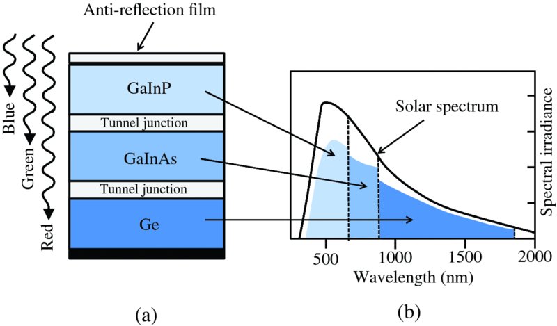
Figure 5.39 (a) The principle of operation of the multi-junction solar cell, which consists of a stack of three sub-cells. The topmost sub-cell is made from a semiconductor that has a large band gap and absorbs photons at the blue end of the solar spectrum. The transmitted photons encounter the middle sub-cell that is made from a semiconductor that has a medium band gap and absorbs lower-energy, green photons. The bottom sub-cell is made from a semiconductor with a low band gap that absorbs the lowest-energy photons, at the red end of the spectrum. The tunnel junctions provide low-loss electrical and optical connections between adjacent sub-cells. (b) The three regions of the solar spectrum that are absorbed by the three different semiconductor materials, each contributing to the photocurrent. The shaded areas represent the electrical power obtained.
Light concentrators
One way to increase the output power of a solar cell is simply to collect sunlight over a large area and concentrate it onto the cell with a lens or mirror. The concentration ratio X is the ratio of the concentrator input aperture to the surface area of the cell. This is an effective technique, as the active semiconductor material is usually the most expensive part of the cell; this is especially the case for multi-junction cells. Concentration of incident light can be obtained with a Fresnel lens or a parabolic mirror, as shown in Figure 5.40. Indeed, a combination of the two may be used, as also shown. Concentration ratios of 1000 or more can be achieved, increasing the light irradiance by the same factor. Such power densities are sufficient to heat up a solar cell substantially and high-capacity heat sinks are necessary to avoid large temperature rises that reduce the efficiency of the cell.
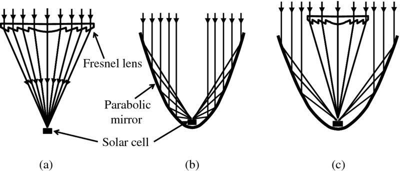
Figure 5.40 Various ways to concentrate solar radiation onto a solar cell: (a) a Fresnel lens, (b) a parabolic mirror, and (c) a combination of the two.
If sunlight is concentrated by a factor of X, it is reasonable to assume that the photocurrent iphoto, and hence the short circuit current isc, is multiplied by the same factor. In addition, however, increasing the incident light irradiance also increases the efficiency of the solar cell. This is because increasing isc also increases the open-circuit voltage Voc. In turn, this increases the fill factor and the power conversion efficiency of the cell. We can see how this increase in Voc arises from Equation (5.27):

If we concentrate the light by a factor X, the resulting open-circuit voltage, V'oc, is given by
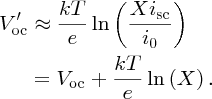
If we take Voc = 0.72 V, kT/e = 1/40 V and X = 1000, we see that V'oc is 24% greater than Voc and the efficiency of the solar cell will increase by a similar factor. The efficiency of multi-junction solar cells using concentrators is now above 40%.
Quantum dot solar cells
Quantum dots are tiny crystals of semiconductor material; the quantum dots used in solar cells have dimensions of about 10 nm. They have electrical properties that make them useful for solar cells, as well as for a wide range of other applications. In particular, the separation of the energy levels in a quantum dot can be controlled. This means that the band gap of a quantum dot may be ‘tuned’ to a particular wavelength range. This is in sharp contrast to semiconductor materials of macroscopic size, which have a fixed band gap. Controlling the band gap offers several possibilities. For example, it can be optimised to match the solar spectrum according to the Shockley-Queisser limit, or a multi-junction cell can be made from stacked layers of quantum dots of steadily reducing band gap.
The band gap can be varied because the allowed energy levels in a quantum dot are governed by the quantum mechanics of particles that are confined to microscopic dimensions. We described in Section 2.2.3 a one-dimensional quantum well. We saw that the allowed energy levels in such a well depend on the width of the well. By changing the width of the well, we change the allowed energy levels and the energy separations between them. The energies and their separations in a one-dimensional well scale as 1/L2, where L characterises the width of the well. In a quantum dot, electrons are confined in three dimensions but quantised energy levels are again obtained. Moreover, their energy levels and separations again scale as 1/L2, where L characterises the size of the quantum dot. To change the band gap in a quantum dot, we simply need to change its size. Quantum dots can be cheaply produced as colloids in a suitable solvent by wet-chemical techniques, and the size of the dot can be readily controlled.
There are a number of solar cell designs that use quantum dots. A schematic diagram of one kind is shown in Figure 5.41. The cell consists of quantum dots made from the semiconductor cadmium selenide (CdSe). The quantum dots are attached to nanoparticles of titanium oxide (TiO2), which in turn are attached to a transparent but conducting electrode. The quantum dots and nanoparticles are contained in an electrolyte that typically contains polysulphide ions. These are compounds consisting of chains of n negatively charged sulphur ions with the symbol S2 −n,with n = 2–5. There is also a second electrode made of platinum at the back of the cell.
Figure 5.41 Schematic diagram of a quantum dot solar cell. The cell consists of quantum dots made from cadmium selenide (CdSe). These are attached to nanoparticles of titanium oxide (TiO2), which in turn are attached to a transparent but conducting electrode. The quantum dots and nanoparticles are contained in an electrolyte that typically contains polysulphide ions. An incident photon excites an electron into the conduction band of a quantum dot, leaving behind a hole in the valence band. This excited electron rapidly moves into an TiO2 nanoparticle. From there the electron passes into the transparent electrode and moves around the external circuit to the platinum electrode. The polysulphide ions serve to transport electrons from the platinum electrode back to the quantum dots.
The operation of the cell is as follows. An incident photon excites an electron into the conduction band of a quantum dot, leaving behind a hole in the valence band. This excited electron lies energetically above the conduction band of the TiO2 nanoparticle and the electron rapidly moves into the nanoparticle. From there the electron passes into the transparent electrode and moves around the external circuit to the platinum electrode. An S2 −n ion from the electrolyte accepts electrons from the platinum electrode via the reaction
The S2 − ions diffuse through the electrolyte and migrate to the quantum dots. There they deliver electrons to fill the holes generated by the photo-excited electrons according to the reactions
where the symbol h+ denotes a hole. This returns S2 −n ions to the electrolyte and the cycle continues. In this way, electrons are transported from the platinum electrode back to the quantum dots.
In another kind of solar cell, called a dye-sensitised solar cell, the quantum dots are replaced by dye molecules. The mechanism in a dye-sensitised solar cell and the structure of the cell are similar to those of a quantum dot cell. Photo-excitation of the sensitised dye results in the injection of an electron into the conduction band of a TiO2 nanoparticle. The electron then moves to a transparent electrode and passes around an external circuit to an electrode at the back of the cell. As before, there is an electrolyte that serves to transport electrons from the electrode back to the dye molecules. Interestingly, research on these dye-based systems began as a way of understanding the mechanism of photosynthesis, Nature's way of harvesting solar energy.
Quantum dot solar cells and dye-sensitised solar cells are presently not as efficient as a silicon solar cell, although their efficiencies are expected to increase with further research and development. However, they do have a distinct advantage. Quantum dots and dye molecules can be readily deposited onto a plastic substrate by spraying or printing. This dramatically reduces module construction costs, especially for large surface area solar cells.
Problems 5
-
(a) Three semiconductor materials that are commonly used in multi-junction solar cells are gallium indium phosphide, gallium indium arsenide and germanium. These have band gaps of 1.89, 1.42 and 0.67 eV, respectively. Calculate the critical wavelengths for these three semiconductors. (b) At what wavelength would you expect silicon to become transparent to solar radiation? The band gap of silicon is 1.11 eV.
-
The work function of copper is 4.7 eV. (a) What is the maximum wavelength that an incident photon can have if it is to produce a photoelectron? (b) One type of particle accelerator that is used to produce a beam of high-energy electrons utilises the photoelectric effect for its source of electrons. In this source, a beam of UV radiation (λ = 226 nm) from a pulsed laser is incident on a copper surface. There are 500 laser pulses/s and each pulse contains 5.0 × 10− 4J of energy. Given that the quantum efficiency, defined as the number of photoelectrons produced per incident photon, of the copper surface is 1.5 × 10− 3, calculate the mean current of the electron beam in the accelerator.
-
Light of wavelength 550 nm is incident upon a slice of silicon. What are the frequency and wavelength of the light within the slice? The refractive index of silicon is 3.42.
-
A phosphorus atom replaces an atom of silicon in the lattice of a silicon crystal, giving rise to a loosely bound electron. Use the modified Bohr model of the hydrogen atom to calculate the Bohr radius of this electron. The relative permittivity, ϵ, of silicon is 11.8 and the effective mass, m*e, of the electron is 0.26 me. The Bohr radius, a0, for the hydrogen atom is 0.53 × 10− 10 m.
-
The impurity concentration in a semiconductor has to be relatively low; at low concentration, the impurity atoms produce discrete energy levels, but if the impurity atoms are sufficiently close, their energy levels spread into bands. Use the modified Bohr theory of the hydrogen atom to estimate the maximum concentration of arsenic impurities in germanium that avoids overlap between adjacent impurity atoms. The relative permittivity, ϵ, of germanium is 15.8 and the effective mass, m*e, of the electron is 0.55 me. Germanium has a density of 5.32 × 10³ kg/m3 and its atomic weight is 72.6 u.
-
(a) The band gap of gallium arsenide is 1.43 eV and the effective masses of the electrons and holes are 0.067 me and 0.48 me, respectively. Find the intrinsic concentrations of the electrons and holes. (b) Compare your value with the number of free electrons in copper, assuming each copper atom gives rise to a free electron. The density of copper is 8.96 × 10³ kg/m3 and its atomic weight is 63.55 u.
-
The effective masses of the electrons and holes in germanium are 0.55 me and 0.37 me, respectively, and the band gap is 0.67 eV. A sample of germanium is doped with donor impurity atoms at the concentration 1.4 × 10²³ atoms/m3. What is the hole concentration when the sample is at equilibrium at T = 300 K?
-
Intrinsic semiconductor gallium arsenide has a band gap of 1.43 eV. Use the Fermi–Dirac distribution to calculate the probability that a state at the bottom of the conduction band is occupied by an electron at a temperature of 300 K. By how much does the probability increase if the temperature is raised by 10 K?
-
The effective mass of a charge carrier in a semiconductor can be obtained from a measurement of its cyclotron frequency when a magnetic field is applied to the semiconductor. When a magnetic field of 1.5 T is applied to a sample of indium arsenide, the cyclotron frequency of the donor electrons is found to be 1.32 × 10¹³ rad/s. What is the effective mass of these electrons?
-
A crystal of pure germanium can be used to measure the energy of γ-rays. The principle of operation is that the γ-ray produces electron–hole pairs as it passes through the crystal. This gives rise to a current pulse that is measured by a charge sensitive preamplifier in an external circuit, as illustrated in the figure. Suppose that a 660 keV γ-ray emitted by a 137Cs nucleus loses all its energy in passing through a slab of germanium by producing electron–hole pairs. Calculate the number, N, of electron–hole pairs that can be generated. According to Poisson statistics, the number of electron–hole pairs generated will have statistical fluctuations given by
 . Hence, estimate the energy resolution of a germanium detector at 660 keV. Explain
why is it important to maintain a germanium detector at the temperature of liquid
nitrogen and why the energy resolution of a germanium detector is better than that
of a silicon detector.
. Hence, estimate the energy resolution of a germanium detector at 660 keV. Explain
why is it important to maintain a germanium detector at the temperature of liquid
nitrogen and why the energy resolution of a germanium detector is better than that
of a silicon detector.
-
A light-emitting diode (LED) is essentially a forward-biased p–n junction. As electrons cross from the n-region to the p-region, they combine with holes generating light. (a) Given that the band gap of gallium arsenide is 1.43 eV, what is the wavelength of the emitted light and in which region of the solar spectrum does it lie? (b) If a battery provides a current through a gallium arsenide LED of 5 mA, what will be the total power of the emitted light, assuming that 10% of the electrons generate a photon? (c) What band gap would be required for a semiconductor to produce violet light? Suggest a suitable semiconductor. Note: Isamu Akasaki, Hiroshi Amano and Shuji Nakamura were jointly awarded the Nobel Prize in Physics, 2014 ‘for the invention of efficient blue light-emitting diodes….’
-
Silicon has a linear attenuation coefficient of 3080/cm at wavelength 653 nm. (a) What thickness of silicon crystal is necessary for 99% of incident photons of this wavelength to be absorbed? What thickness is necessary for a crystal of gallium arsenide, which has an attenuation coefficient of 34 468/cm at this wavelength?
(b) Assuming that the absorption of a photon leads to the generation of an electron–hole pair, how many electron–hole pairs are produced per second in the first 1.0 μm of a silicon crystal of area 100 cm2, when 25 W of radiation of wavelength 653 nm is incident upon the crystal? What is the mean rate of generation per unit volume?
-
In a quantum dot, the electrons are confined within three dimensions. The allowed energy levels of the electrons have the form
where m*e is the effective mass of an electron and is equal to 0.65 me. Suppose that a particular quantum dot has dimensions 8 nm × 8 nm × 6 nm. (a) Calculate the energies of the first three levels. (b) What is the wavelength of the photon emitted in a transition between the lowest two levels?
-
The rated power of a solar cell is its maximum power output with an incident solar irradiance of 1000 W/m2. A particular solar cell has a power rating of 50 W. What maximum power would the module produce at a manned station on Mars? The mean distances of the Earth and Mars from the Sun are 1.5 × 10¹¹ m and 2.28 × 10¹¹ m, respectively. Note that Mars has no significant atmosphere.
-
A particular solar cell has a reverse saturation current, i0, of 1.0 × 10− 10 A. The photocurrent iphoto when the solar cell is irradiated by sunlight is 2.0 A. Taking the temperature to be T = 300 K: (a) determine the short circuit current isc and the open circuit voltage Voc; (b) calculate Vmp and the imp, the values of voltage and current for maximum power; (c) make a plot of the solar cell equation
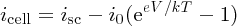
over the range of icell from icell = 0 to icell = isc, to show how the cell voltage V varies with load current icell. Mark on the plot isc, imp, Voc and Vmp. Calculate the fill factor for the solar cell. Determine the number of solar cells required for a module that provides a nominal voltage of 12 V. What would be the optimum load resistance for this module?
-
Making reasonable assumptions, estimate the area of the solar cells that are needed on a south-facing roof to provide an electrical power of 3 kW to a household.
-
Compare and contrast solar water heaters and photovoltaic cells for the purpose of harvesting solar energy.