Chapter 3. How Electronic Products Are Manufactured
Back in the 1980s, a family friend went to work as an engineer at a major American automaker. Her first assignment was to fix a little problem: an engine part had been designed so that it fit properly in the engine once it was in its correct place. But, unfortunately, there was no way to get the part into its correct place during the manufacturing process. So the engine couldn’t be built in the factory.
Oops.
It’s easy to chalk off this misfire to the general shoddiness that pervaded the American auto industry during those days. In fact, I’d wager that this kind of thing rarely happens at auto companies today, thanks to better CAD tools, rapid prototyping, and smarter processes. But variants of “we can’t actually build this” happen all of the time in product development, and the resulting redesign/redevelopment efforts to address the problems can be costly and frustrating.
This chapter presents an overview of the process typically followed during the factory production of devices that contain electronics and have simple mechanical parts, products like computers, smart phones, or wearable sensors. (Products that have more complex mechanicals, such as cars or heart-assist pumps, will follow processes that are broadly similar but far more complex.)
Since manufacturing occurs at the end of the product development cycle, it might seem out of place to have this chapter at the front of this book rather than toward the end. But there’s a method to this madness: not knowing (or paying too little attention to) the manufacturing process is one of the most important root causes of potholes in product development, often resulting in products being developed that:
-
Are unbuildable or which cost more to build than they should because excessive effort (time) is needed
-
Have reduced reliability (e.g., from cables that tend to not get inserted all of the way and then fall out with use, circuit board features that trap contaminants, etc.)
-
Require redesign soon after launch when components become difficult or impossible to obtain
These problems are largely avoidable by practicing design for manufacturability and design for assembly, DFM/DFA for short. We’ll look at some of the formal practices around DFM/DFA in Chapter 6, but to a large degree DFM/DFA is a mindset that designer/developers should embrace throughout development. Successful DFM/DFA, in turn, mandates that product designers/developers have an understanding of how products are manufactured, and that they work together with their manufacturer(s) during development to ensure that there are no surprises when it comes time to start building.
A word of clarification: the phrases design for manufacturability and design for assembly are used both to denote general activities that improve manufacturability and assembly, and to identify specific optimization practices pioneered by Boothroyd and Dewhurst that we’ll touch on in Chapter 6. In this book, these phrases will be used in both senses, and I’ll try to make it clear which is meant by the context in which it’s used.
My hope is that reviewing the manufacturing process early will help to provide context for the development process described throughout the book.
One more note before we get going: this chapter is heavy on electronics manufacturing, while more information around mechanical manufacturing is found in Chapter 6. The most important reason for this breakdown is that, traditionally, electronic products have had relatively simple mechanical assembly (think smart phones and televisions) and few problems with the mechanical process. In my experience developing products (primarily medical devices with embedded intelligence), electronics manufacturing and “box build” (full system assembly) are typically performed in the same factory using mechanical components manufactured by outside vendors.
Complex electromechanical products (e.g., robots) are becoming more important over time, and these can require extensive and challenging mechanical assembly. But the techniques and processes used for complex electromechanical assemblies can vary significantly from one product to another, whereas electronics manufacturing tends to be more similar from one product to another. While a single chapter can give a pretty good overview of the electronics manufacturing process, a treatment of complex mechanical manufacturing at the same level of detail could easily fill a book of its own. So, if your product is more like a smart phone or television, this chapter should serve as a good overview of the manufacturing process. If your product is more like a robot, this chapter should serve as a starting point, but you should understand that the process will ultimately be substantially more complex.
OK! Enough with the caveats! Let’s get started with an overview of the process.
Manufacturing Overview
Prototypes tend to get assembled via a chaotic process, particularly early in the development cycle. By contrast, products are manufactured via a series of discrete and well-identified steps.
Gaining an understanding of manufacturing is largely a matter of understanding the different steps involved. As a baseline, let’s start by walking through the process that would be followed (more or less) for medium production volumes, say, 1,000–10,000 units per year. After our walkthrough, I’ll describe how things might change when manufacturing in higher and lower volumes.
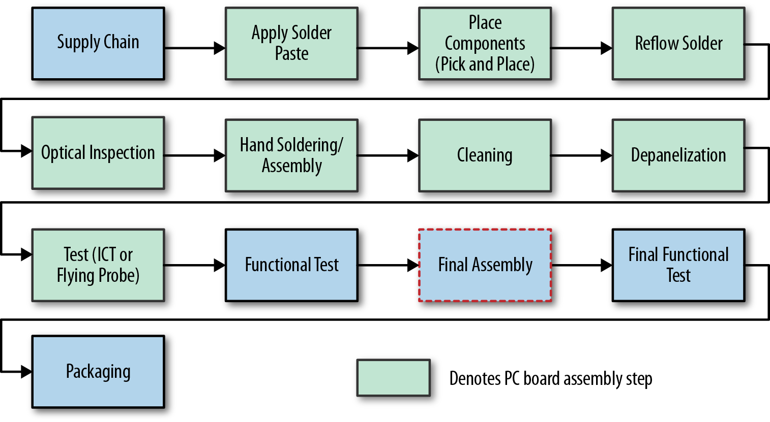
Figure 3-1 shows a schematic overview of a typical process. Most manufacturing follows a pretty similar process, but as we’ll see there can be differences in process between one product and another.

Figure 3-1. Typical manufacturing process steps
Note that builds are usually done in batches; for example, if building a batch of 100 units, 100 units would go through step 1, then the 100 would go through step 2, etc.
Now let’s review each of these manufacturing steps in a tiny bit of detail. So you won’t have to keep flipping back to Figure 3-1 to see where we are in the process, we’ll reproduce the process diagram for each step, highlighting the current step.
Supply Chain

When we think of factories, we think of building stuff. But it turns out that the most challenging part of manufacturing is usually not the building part; rather, it’s getting all of the needed parts into one place, at the right moment, so that the building can happen. That part is known as the supply chain.
We product designers/developers tend to think of the supply chain as simply the people who order parts, but obtaining components is actually much, much more challenging than most of us realize. A typical product consists of hundreds or perhaps thousands of components, which all must come together at the right instant for a unit to be built. If even one sub-penny resistor is missing, production typically won’t happen.
Not only does everything need to show up on time, it all needs to be obtained as economically as possible. In theory it’s just about finding a good price and placing an order, but reality is a lot more complex. Here are some of the challenges faced by supply chain staff:
-
Components come from multiple vendors; often dozens of vendors supply parts for a single product.
-
Components normally constitute the largest cost of building a product, so buyers need to negotiate good pricing or else the product will cost significantly more than necessary.
-
Components can suddenly become unavailable from a source (e.g., a distributor sells its entire inventory to a large customer, an earthquake damages a vendor’s factory, etc.), and alternative sources must be found quickly or production pauses.
-
Components can go obsolete. Supply chain resources must manage the process of identifying and qualifying alternative sources of identical parts, and/or work with engineering folks on a redesign to accommodate a new part.
-
Components have different lead times (the time it takes to receive them once they’ve been ordered). Common components are available next-day, or even same-day, while some items like custom LCDs might take months. And if the LCDs show up with a defect? It can take months to get replacements without the defect.
-
Ensuring that parts are genuine. Counterfeit parts exist, and can compromise safety and reliability. Finding out that a shipping product contains counterfeit parts can lead to a recall and other misery.
Life would actually be pretty easy if, at the start of the project, we could order all of the parts we’d ever need to build all the units we’ll ever build, put these parts in inventory, and then draw down that inventory as we built units. We’d never have an interruption in our supply, because all components would always be on hand. The problem is that inventory is a bad word among financial and management types: inventory’s usually been paid for (or at least we owe money for it), but inventory won’t generate revenue until it’s built into something. So it represents money that’s just sitting on a shelf, being unproductive and taking up space. In an ideal financial/managerial world, parts would show up at the loading dock the day they’re used and never need to sit in inventory for more than a few hours.
In the real world, inventory is a complex juggling act. Perhaps only a few days’ worth of inventory is kept on hand for parts that are easily available and/or at low risk of having deliveries interrupted, while larger supplies are kept of components that are less common or are otherwise at higher risk of having their supply interrupted. Supply chain folks can work out various deals with component makers and distributors to ensure we have parts to build with while maximizing financial health. In many cases we can negotiate deals that (almost) guarantee a steady supply of components without our having to hold substantial inventories.
Once the supply chain is worked out and we have parts in hand, the building can begin.
Building Circuits: PCB Assembly
Electronics lie at the physical heart of the kinds of products we’ll be covering in this book. Since they’re so important, let’s review a little nomenclature to put us all on the same page, and then we’ll delve into some of the details of how electronic assemblies are built.
Electronic circuits are built by soldering components to a printed circuit board (a.k.a PC board or PCB). Once components are soldered to the PCB, the assembly is sometimes referred to as a PC board assembly (PCBA) or less commonly a printed circuit assembly (PCA). Figure 3-2 shows a PCB, and the PCBA created by soldering components to that PCB.

Figure 3-2. Bare and assembled printed circuit board (PCB and PCBA) (credit: Pyramid Technical Consultants)
Confusingly, sometimes PCB is also used to refer to a PCBA. The context in which it’s used should make it obvious as to whether PCB is referring to the unpopulated board or built assembly. In this book, PCB will always refer to a bare board, while PCBA will always be used for an assembled board. But in real life, it’s always good to ask for clarification if an acronym’s usage is not totally obvious.
PCBs are custom components ordered from specialized vendors, manufactured based on CAD files supplied by the product developer. The process of assembling electronics components onto these boards is called, boringly enough, PCB assembly. The name of this task might be boring, but the actual assembly can be anything but boring if we’re unlucky.
The object of PCB assembly is to make sure that:
-
All parts are in the correct place, and in the correct orientation.
-
All component pins are soundly soldered to the correct pads on the PCB.
-
There’s no extra solder that can cause trouble, say, by shorting things out (connecting together component pins or other conductors that are not supposed to be connected).
-
There’s no extra anything else, such as solvents or flux used in manufacturing, which can cause trouble by conducting current where there shouldn’t be any, generating corrosion, and so forth.
For all but the smallest quantities, PCB assembly is almost entirely automated. Boards and components go into one end of an assembly line, and finished boards come out of the other end with a minimum of human intervention.
The first step in the assembly process is to apply solder paste to the PCB.
PCB Assembly: Solder Paste Application

Solder is a metal alloy that’s used to electrically and mechanically connect metal parts together. In particular, it’s used to form sturdy, highly conductive bonds between component pins and metal pads on the PCB. Solder paste is a goopy mix of ultrafine powdered solder mixed with liquid flux, the flux’s job being to clean any corrosion or contamination from the metal surfaces so that a good solder joint can be made.
The first step in the PCB assembly process is to add the right amount of solder paste to the board in the right spots. This is done using a solder stencil, which is custom to each PC board design. The solder stencil is a thin metal sheet with cutouts wherever solder paste should be applied to the board (e.g., on every board pad that will connect to a component lead). Figure 3-3 shows a solder stencil.

Figure 3-3. Solder stencil (credit: Alan Walsh)
The stencil is laid precisely on the board, the paste is smeared evenly across the stencil using a squeegee, and then the stencil is removed and cleaned. The board now has the right amount of solder paste in the right places. Figure 3-4 shows solder paste being applied to a board with an automated squeegee. Because the stencil’s silver, it’s a little hard to see in the picture that the gray solder paste is filling in the stencil’s holes.

Figure 3-4. Solder application (credit: Alan Walsh)
Now that the solder paste is down, we can place the board’s components.
PCB Assembly: Placing Components

The next step is to place each component in the right spot on the PCB, which is normally accomplished by a pick-and-place machine. The components to be placed are typically supplied on reels of tape known as tape-and-reel packaging. Figure 3-5 shows some example reels in use on a pick-and-place.

Figure 3-5. Component reels in a pick-and-place machine (credit: Alan Walsh)
Figure 3-6 shows a close-up of resistors packaged as tape and reel. Each component is held in an embossed pocket in the carrier tape. Each pocket is sealed with a cover tape (usually clear) that’s peeled up just before the part is picked and placed.

Figure 3-6. Close-up of components on tape (credit: Alan Walsh)
Beyond being supplied with the right components, the pick-and-place machine also needs to know which parts go where. This programming is usually accomplished using CAD data automatically generated as part of our Electronics/PCB design application, along with our bill of materials (parts list), which is also usually generated by our Electronics/PCB application.
Tubes and/or trays, shown in Figure 3-7, are sometimes used instead of tape and reel to hold parts for the pick-and-place. Depending on the specific model of pick-and-place, tubes and/or trays typically don’t work as smoothly as tape and reel. If using tubes and/or trays is of interest, this should be explored in advance with the folks who’ll be doing your manufacturing.

Figure 3-7. Tube and tray
Each PC board is positioned in the pick-and-place machine, and then each component is picked up from its tape using a tiny suction cup, placed onto the right spot on the board, and then released. Figure 3-8 shows the suction cup in action. The solder paste under the placed part conveniently serves as adhesive to hold the part in place temporarily until the solder paste is made solid by reflowing it (discussed in a moment). In some cases, if solder paste isn’t sufficient to hold a part down (e.g., a large part with few pins), the pick-and-place might put down a bit of adhesive to help out.

Figure 3-8. Pick-and-place suction cup holding IC
Pick-and-place machines are fast and accurate, the fastest being able to place hundreds of parts per minute, but there are a few tradeoffs we need to deal with in exchange for this great speed. First off, pick-and-place machines only work with surface-mount devices (SMDs), not the larger through-hole parts that are popular for prototyping. Through-hole parts are usually placed and soldered by hand, which is much more expensive than automated SMD processes. Switching from through-hole parts to their SMD equivalents is usually not a big deal, just something that should be done during PC board design.
The second issue is that all the reels (and tubes/trays if used) must be loaded onto the pick-and-place before it can begin work, which takes some time. This setup time is the same whether we’re assembling one board or 1,000, so building fewer large batches tends to make more sense than building many small batches.
A third issue is that pick-and-place machines only accept a finite number of reels, perhaps 20 to 100 or more depending on the model. If we have more unique parts than the number of reels the machine can support, we’ll need to run the boards through the machine multiple times to get all the parts placed. To avoid multiple passes, it’s a good idea to reduce the number of different parts during design/development by using the same parts as often as possible; for example, we can try to standardize on a few resistor values and sizes, putting several in parallel or serial to create different resistances if needed.
A fourth issue, and often the biggest surprise to people new to this game, is that we sometimes can only purchase full reels of parts even though we might only need a smaller number for our build. By default, parts come on reels in quantities that range from hundreds to thousands of pieces per reel. A full reel of resistors might contain 5,000 pieces, but because resistors cost a fraction of a cent, the entire reel should cost less than $10, which is not a big deal. But a $12 GPS chip that comes in reels of 500 will set us back $6,000 per reel, even if we only need 100 parts. Our $12 GPS chip is now $60, unless our supply chain folks can find a way to resell the parts to someone else.
Fortunately, alternatives to full reels are often (but not always!) available. Component distributors will usually sell a strip of tape cut from a reel in the size we want (called a cut tape), or create a smaller reel for us using a cut tape. As mentioned previously, chips can also be supplied in custom quantities in tubes and/or trays, although these will not play nicely with all pick-and-place machines.
We now have PCB, solder, and components. Our ingredients are mixed; next, it’s into the oven to bake.
PCB Assembly: Reflow

Reflow is the process of converting gloopy solder paste to solid solder joints. In particular, it involves heating the PC board and components in a way that will:
-
Activate the flux so it does a better job of cleaning, and then vaporizes away.
-
Melt the ground solder in the paste to liquid, then cool it to solidify as a single chunk that binds the component lead to its pad.
In practice, this is bit more complex than simply getting the board to a certain temperature and cooling it down. Heating and cooling should follow a profile that ensures that:
-
Components don’t heat or cool too quickly, which can cause failure from thermal shock.
-
The flux has adequate time at an elevated temperature to properly clean and then evaporate.
-
The heat has time to soak into the entire board surface; i.e., the entire board gets to the desired temperature. If we don’t soak the board sufficiently, some parts of the board might not get hot enough to create a good solder joint.
Figure 3-9 shows a typical graph of temperature versus time during the reflow process.

Figure 3-9. Typical reflow profile (credit: Wikimedia Commons)
Solder reflow is accomplished using a reflow oven. The oven is programmed with the desired temperature profile depending on the type of solder paste being used and other factors. Beyond programmability, reflow ovens must also be designed to ensure that each board is heated evenly. Heating is typically accomplished using hot gas convection (either air or nitrogen), but other methods can be used as well. Reflow ovens come in a wide variety of sizes depending on throughput, from batch units as small as a microwave oven, to large continuous-throughput units like the one shown in Figure 3-10.
Large commercial units that reflow a continuous stream of boards on a conveyor belt (rather than a single batch at once) have multiple zones set to different temperatures, as called out in the reflow temperature profile. If you look carefully under the open top in Figure 3-10, you’ll notice the back ends of fans sticking up; these fans move air within each temperature zone to keep temperature even within that zone.

Figure 3-10. Large continuous reflow oven with the top propped open (credit: Alan Walsh)
Once out of the oven, our board has hundreds or thousands of newly soldered joints. Are these joints all good? Are the parts still all where they’re supposed to be? Sometimes not: better check ’em out, which we’ll do next.
PCB Assembly: Optical Inspection

Once components are soldered down, an automated optical inspection (AOI) station examines the board to check if our parts ended up looking properly soldered, and in precisely the right places. It will note any parts whose position or orientation is incorrect, so that they can be touched up by hand (called rework), or the board scrapped. Figure 3-11 shows an example of AOI output as seen by the machine operator. In this case, the AOI has spotted a part which looks different than it’s seen in previous boards, and it’s zoomed in on this part and is asking the technician to take a look and enter a verdict: is there a problem with the way the part is assembled to the board, or is this change OK?

Figure 3-11. AOI screen (credit: Alan Walsh)
This time the difference is innocent: the part that’s flagged (a resistor network) is produced by many vendors, and a new vendor was used for this particular build. The problem flagged is that the “103” marking on the part is simply in a different font than the AOIs previously seen for this PCBA. If we instruct the AOI machine to memorize this new style of “103,” this part won’t be flagged for the same reason in the future PCBAs.
Note that while this difference is innocent, little things like this can sometimes halt production until a phone call is made to the right person in design/development to confirm all is OK. In other instances, an AOI operator might decide without checking with someone who knows that an issue is similarly cosmetic when it’s truly a serious build issue, and we end up with a batch of bad boards. In manufacturing, every detail counts!
Parts with contacts that are hidden from view can be a challenge to inspect, of course. The classic example of tough-to-inspect is chips with ball grid array (BGA) packages, which can have more than a thousand soldered contacts all hidden beneath the part; the bottom view of a smaller BGA part is shown in Figure 3-12.

Figure 3-12. BGA, bottom view (credit: Wikimedia Commons)
Figure 3-13 shows the PCB footprint of a medium-sized BGA, a few hundred balls. The difficulty in inspecting all of those solder joints once they’re lying under a square slab (the BGA package) should be obvious.

Figure 3-13. Medium ball grid array footprint (credit: Pyramid Technical Consultants)
Specialized 2D and 3D x-ray systems are used to inspect the invisible. Figure 3-14 shows a portion of an x-rayed reflowed BGA. The red arrows point to solder bridges where two contacts are accidentally soldered together; either this board will be reworked or scrapped.

Figure 3-14. BGA x-ray (credit: Lightspeed Manufacturing)
Note that not all factories have x-ray systems; that’s one item to look into when selecting a contract manufacturer.
At this point, we’ve assembled what we can on the PCB via automation, and we have a list of any gross defects introduced during that process. Next we’ll rely on that most amazing machine of all—humans—to finish off board assembly by doing what the robots couldn’t.
PCB Assembly: Hand Soldering and Assembly

In many instances, a board will require that some work be done by hand, such as:
-
Rework of improperly reflowed parts as flagged in AOI.
-
Rework due to design changes made after PC boards began fabrication. For example, PC board traces might be cut and wires added (known as cuts and jumpers) to change circuit paths. Figure 3-15 shows an example of wiring added as rework.
-
Hand soldering of components that are not suitable for reflow. Examples include through-hole parts and temperature-sensitive parts such as batteries.
-
Hand assembly of mechanical parts on the PCBA.

Figure 3-15. Example PCB rework
As mentioned previously, it’s much more expensive to do things by hand than by machine, so designers/developers should take care to reduce the number of parts that require manual work during assembly; but some hand work usually can’t be avoided. For example, connectors accessed by end users (e.g., USB connectors) are often through-hole rather than SMD to add strength and reduce the odds of the connector coming off the board through wear and tear.
At this point, our board assembly is complete unless we find a defect during later testing that sends the board back for rework. The next two steps, cleaning and depaneling, prepare our PCBAs for assembly into the larger product.
PCB Assembly: Cleaning

A clean PCBA is a good PCBA. In particular, it’s a good practice to wash the PCBA after its assembly to remove any solder flux not burned off during reflow. Flux on the board might cause corrosion and/or unwanted electrical paths, which can affect reliability and performance.
Some fluxes are designated as no-clean because they shouldn’t corrode if left on a board and do not conduct substantial current; however these are usually cleaned anyway because they might still affect sensitive or high-speed circuitry.
PCB Assembly: Depaneling

It’s typically most economical to fabricate and assemble PCBs as panels of multiple boards, the individual boards being cut or broken out sometime after assembly. The number of boards per panel depends on the sizes that the PCB fabricator and assembler can accommodate, the size of each PC board, and sometimes other factors. For example, an 18” × 24” panel can accommodate up to 20 PCBs that are 2.5” × 5” each (with some space to spare).
Figure 3-16 shows a panel of five long, narrow boards. Note that there’s a scored line between each board, and a bit of routing (openings cut through the panel) at each board’s corner.

Figure 3-16. Five PCBs in a panel (credit: Pyramid Technical Consultants)
Scoring consists of cutting a shallow V-shaped grove across the board, which makes the board easy to snap apart at that line. Routing uses a tool to cut a channel clear through the board.
Figure 3-17 shows a single board after depaneling.

Figure 3-17. Single PCB after depaneling (credit: Pyramid Technical Consultants)
PCB assembly is performed while the PCBs are still together in their panel. At some point, often before test (discussed in a moment), the individual boards are cut apart using a depaneling tool, or are simply snapped apart by hand (which is more stressful for the board and its components). Depaneling tools employ various means for removing boards, including sawing, routing, cutting with a “pizza cutter” wheel laser, and punching out using special fixtures.
The process of paneling and depaneling has a few important implications for designers/developers pertaining to the edges of the individual boards separated out by the process.
The PCB edges that are cut or broken apart can experience a good bit of stress and strain during the depaneling process, which can cause mechanical deformations close to those edges. It’s a good idea to keep a margin of at least 50 mil (0.050 in) between board edges and traces/pads, and at least 100 mil between board edges and components. (Note that PCB measurements are pretty universally called out in mils, which equal thousandths of an inch. Yes, the PCB world still works in inches!)
Other issues have to do with tradeoffs between separating boards via scoring versus routing:
-
Routing produces smooth edges versus rough edges for scoring, which is normally only an issue if boards will be seen by the end user, say, if they plug into a connector.
-
Routing requires greater spacing between boards (to accommodate the width of the routing tool).
-
Routed panels can have significant flex, which can cause issues with PCB assembly.
To avoid problems, it’s important to work with your assembler when designing PCB panels. They’ll have a good idea of what will work on their equipment.
Our PCBAs are now complete, or at least they look really good. Now it’s time to see whether they work as good as they look.
Test
PCBAs are complex, and normally each will be tested to make sure that the assembly process went according to plan. Note that this factory testing is normally quite different than the testing performed in our lab to ensure that our design is correct (design verification testing).
The range of effort brought to bear on factory testing can vary tremendously. Factory testing can be as simple as having a technician turn on a product after final assembly to see if things seem to work. On the other end of the spectrum, factory test can probe every nook and cranny of each manufactured unit before it ships to make sure that everything’s in good order. The degree of testing largely depends on the likelihood of problems occurring in manufacturing, and the cost of finding these errors once the unit leaves the factory. For example, the occasional failure of an inexpensive toy is probably not a big deal as long as it’s not a safety issue, so we probably wouldn’t put forth much of a test effort. But even the occasional failure of a computer module that controls automobile braking would be something we’d really want to avoid, and thus a serious factory test effort is in order.
Large factory test efforts can sometimes rival the size (and cost) of the efforts to design/develop the product itself. For these efforts, it’s useful to employ the help of specialized test engineers who are experienced with the world of factories and factory workers, a much different constituency than most other end users.
There are two basic types of testing, in-circuit and functional, that can be performed on the PCBA, depending on the product. We explore these in the next sections.
In-Circuit Test (ICT)

ICT is used to demonstrate that PCBAs are built correctly by analyzing electrical characteristics such as the resistance of each solder joint. High-volume ICT is most commonly performed using a bed-of-nails tester, in which a large number of probes are placed on the PCBA simultaneously—up to several thousand in some test setups. Various test signals are introduced into some probes, and responses measured at other probes.
The probes are typically spring-loaded and set into a special board called a test fixture, usually custom-made for each PCBA design. Each probe connects to the circuit being tested (sometimes called the device under test/DUT, or unit under test/UUT) by touching a conductive patch on the board, normally either:
-
A via used by circuit board designers to run a signal from one PCB layer to another, which also happens to serve as nice test point
Figure 3-18 shows a bed-of-nails system in action, and Figure 3-19 shows some test pads and vias which are used for probe contact to the PCB.

Figure 3-18. Bed-of-nails tester (credit: SPEA)

Figure 3-19. Placeholder for test pads (filled gold circles) and vias (gold circles with a hole through them) (credit: Altzone licensed under CC BY-SA 3.0)
The board and test fixture are brought into precise contact with one another and then test software runs through a programmed sequence designed to uncover problems with the board, which can include shorts or opens (e.g., leads lifted from pads), bad component orientation (which sometimes can’t be caught in AOI), wrong component values, defective components, and signal integrity issues (i.e., do signals propagate properly to destinations on the board without undue degradation).
Experienced designers/developers try to design product PC boards that permit every electrically unique spot on the board (called a net by electronics folks) to be accessible by a probe, but this often cannot be achieved due to various constraints, such as the size of the board (“Sorry, we can’t fit another test pad in. We’re too cramped for space!”).
Since ICT electrically access most or all pins on all components, its connections can also be used to program devices such as flash memory, to perform calibrations and tuning, and to run functional tests (covered next).
Functional Test

Functional test focuses on the higher-level functionality of the board beyond the direct testing of whether components are properly soldered into place. For example, a functional test might involve loading some test firmware into a processor that’s part of the PCBA being tested, having that processor run diagnostics on memory and peripherals, and then outputting the results to a computer via serial port. The PC, in turn, flashes a big green PASS or big red FAIL on its screen, and records the detailed test results to a database for analysis.
Functional test ensures that a range of parts are working together correctly as a system. It can also be used to implicitly test circuitry that could not be tested during ICT because of nets that are inaccessible to probes. For example, if a test point is not available to access the net that includes pin X of a certain chip, functional test can implicitly test that pin by running an operation that can only succeed if pin X is soldered to the board and functioning properly.
The downside of functional test is that it tends to not test board connections as thoroughly as ICT does. The safest bet is to perform both ICT and functional test. Later in this chapter when we discuss lower-volume productions we’ll look at the tradeoffs of skipping ICT and going exclusively with functional test.
Functional test can be performed as part of ICT, or at a separate station by communicating with the PCBA via serial port, USB, Ethernet, or similar connection. For most products, a final functional test is run after a device is fully assembled. In many cases, functional tests are also performed at interim points during manufacturing. For example, each PCBA in a multiboard system might undergo its own functional test to ensure that it’s assembled properly, and then the system is tested again as a whole after final assembly to make sure that the boards are assembled together properly.
Burn-in testing
In some instances, boards are allowed to operate for hours, days, or longer while undergoing functional test, sometimes under stressful conditions (e.g., at hotter temperatures than normally encountered). This might be done for a number of reasons, but most often it’s to encourage marginal boards to fail before they leave the factory, which is much better than to fail in a customer’s hands.
Well-designed boards rarely require burn-in, but there are exceptions. For example, if a board is going into an application where the cost of failure is tremendous, such as in a satellite, burn-in might be a good idea to reduce an already small possibility of failure in shipped devices.
Final Assembly
In final assembly. a.k.a. box build, PCBAs and mechanical components are assembled into a finished unit, typically by hand. This can take anywhere from a few minutes for simple devices to several person days or longer for sophisticated systems such as scientific instruments.
Through each step, workers carefully follow assembly instructions, diagrams, and/or videos to ensure that each unit is built correctly. This documentation is best produced as a joint effort between designers/developers and factory staff, and time should be budgeted for this activity during project planning.
There are often checks during the process to ensure that things are, in fact, being assembled correctly: for example, we might check a voltage right after attaching an internal cable to ensure that the connection is good, so we don’t wait until after our product is fully assembled to find that it’s a bad connection (whereupon we’ll need to pull it back apart).
It’s important to take care during design/development to make the assembly process easy and efficient. First off, final assembly is typically the most labor-intensive step in manufacturing, so anything we can do to shorten the time of this task can yield significant savings. This is where design for assembly comes into play, as discussed earlier in this chapter and in Chapter 1.
Second, a more complex assembly increases the quantity of assembly instructions that we must produce for the factory. It’s critical that technicians have unambiguous instructions on how to build the product, and creating these instructions is easier if assembly is simple and straightforward.
Finally, product reliability can be compromised if assembly is tricky. For example, if a technician’s hand cannot get direct access to a connector when it comes time to mate with its cable, she might need to place the cable and lock it into place using a small pliers poked through an opening. This can easily lead to a connection that’s much less reliable than if it we’d considered this step beforehand and designed the product for good access during assembly.
Final Functional Test

As mentioned earlier, a final test sequence, often called end-of-line test, is typically performed after final assembly. While technically this is part of functional test, I’ve broken it out in our diagram since it tends to be more manual and subjective than other functional tests.
In this step, a technician usually checks the overall fit and finish of the device (e.g., all parts seem to be properly put together—no scratches, and so forth), and then turns the device on and perhaps performs some simple operations to make sure that all seems OK. Normally there’s a checklist for the tester to follow, but much of the testing is subjective and therefore tricky to quantify. For example, one tester might notice a faint scratch, whereas another tester might not. Achieving reasonable consistency of pass/fail pronouncements between testers and over time is the challenge here.
Once we’re successfully through final functional test, we have a product to ship. Next, we’ll box it up to ensure that our unit remains attractive and functional while on its way to its new owner.
Packaging

Finished units are made ready for sale by assembling them into a box along with associated parts, manuals, protective foam, bags, etc. These product boxes, in turn, are usually placed into shipping cartons.
Packaging is usually pretty straightforward: bagging, taping, folding, and so forth. It’s usually a fully manual step, thus taking a little care to make the job easy can pay good dividends in fewer missteps, (e.g., fewer boxes missing items) and reduced manufacturing costs.
All boxed up, our units are finally ready to turn into revenue!
More, and Less
Now that we’ve reviewed a general process for manufacturing in medium volumes, let’s look at how things might change for higher and lower volumes.
How Many?
While the basic manufacturing tasks are similar no matter what our build quantity is, the way in which these tasks are accomplished can vary quite a bit depending on yearly or lifetime production volumes. As quantities increase, the use of automation tends to increase with it. (PCBA complexity can also impact automation; e.g., building a small number of PCBAs that each contain an unusually large number of components, or components that require particularly careful treatment, might each benefit from substantial automation.)
Suppose that we have a manufacturing task that can be performed, by hand, in one minute. If we expect to only build, say, 100 units of that product over its lifetime, such as in the case of a communications satellite, spending $10,000 to automate this task doesn’t make sense. US contract manufacturer labor costs are in the ballpark of $1 a minute, so we’d be spending $10,000 to save $100 over the product’s lifetime. However, if we expect to build 1 million units over the product’s lifetime, such as in the case of a portable disk drive for consumer use, then our $10,000 investment in automation will save $1 million in manufacturing costs, which is a very good bargain.
For purposes of thinking about the relative production volumes, the following categories will be used in this book:
-
Very high volume: >100,000 per year
-
High volume: 10,000–100,000 per year
-
Medium volume production: 1,000–10,000 per year
-
Low volumes: 100–1,000 per year
-
Protoduction (so called because production techniques are somewhat similar to prototype production): < 100 per year
Note that these are not standardized categories or numbers. For example, when a huge contract manufacturer (CM) that builds cell phones hears “low volume,” they might think in terms of fewer than 100,000 units per year, whereas a small specialized CM might translate “low volume” into under 100 per year. When communicating with others about manufacturing volume, it’s important to provide ballpark numbers to ensure that everyone’s on the same page.
Higher-Volume Production
Higher-volume production is substantially similar to the preceding process, but with an increased emphasis on automation and inventory control.
-
Supply chain will have more effort devoted to managing inventory, since inventory can become a large investment of perhaps millions of dollars. The supply chain staff at both the company that sells the product and its contract manufacturer will likely include more people. The two organizations will become much more “cozy” with each other, and with component suppliers, in order to ensure that inventory is minimized and supply of components and finished products are not interrupted.
-
There will be a greater emphasis on tweaking the design even after manufacturing is running smoothly to cut costs, improve quality, and/or account for component shortages. Supply Chain will have a close ongoing relationship with designers/developers or with a sustaining engineering group specifically charged with supporting and improving ongoing production.
-
Work performed by hand at lower volumes might be automated. For example, components that are not amenable to reflow soldering in an oven might be soldered using automated selective soldering technologies.
-
There will be more emphasis during the design/development process on reducing the need for hand work (i.e., DFA as discussed in this chapter’s “Final Assembly” and in Chapter 1).
-
To reduce the number of assemblies that need repair or are scrapped, greater efforts will be made to collect and analyze statistical quality data. The results will be used to improve the design/development and manufacturing processes.
Lower-Volume Production
In lower-volume production, the focus is the opposite of high-volume production; the emphasis is on reducing fixed costs that are difficult to recoup due to the small number of boards that will be built. This typically means more manual work. Here are some tactics that can be suitable for lower-volume production:
Relaxed inventory control
Low-volume products tend to be high-priced products, and the cost of parts is typically a smaller percentage of total product cost as compared to higher-volume products. Also, the effort (i.e., cost) of having professionals carefully manage inventory will end up being fairly high when looked at on a per-unit basis. So the best bet is usually to not be in a position where inventory must be carefully managed.
Keeping a relatively large inventory of parts, e.g. always having at least six months’ worth on hand, will reduce the risk of an interruption of inventory that becomes an interruption of shipping products. Potential reengineering and retooling costs associated with parts becoming unavailable can be avoided altogether by purchasing enough parts to build as many units as is anticipated for the rest of the product’s life; this is called a lifetime buy. At the very least, if we ask, manufacturers and distributors will notify us when a part is going obsolete (called an end-of-life [EOL] notice) so manufacturers can have the opportunity to plan, including purchasing sufficient inventory.
Substituting flying-probe ICT for bed-of-nails
In flying-probe testing, shown in Figure 3-20, several robotically controlled probes “fly” around the board, making electrical measurements at exposed metal features such as component pins, vias, test points, and so forth.
The advantage of flying probe versus bed-of-nails is that the former does not require an expensive custom test fixture with hundreds or thousands of precisely located probes. Instead, the positions to be touched with the probes are programmed into a computer: the PCB database is pulled into the test system, and a test engineer indicates the points to be probed and the tests to be run. Also, because the per-board customization is only in software, flying-probe tests can be updated with relatively minimal effort when a board design changes, whereas bed-of-nails fixtures require rework (or even a new fixture) when a board design is updated.

Figure 3-20. Flying probe (credit: SPEA)
The disadvantages of flying probe versus bed-of-nails include:
-
Flying probe is relatively basic compared to bed-of-nails, because fewer points on the circuit are being tested simultaneously, but it can perform a good range of tests including finding open circuits and shorts, verifying resistor and capacitor values, and some more advanced testing.
-
Flying probe takes quite a bit more time as probes are moved from test point to test point, rather than contacting all test points at once. This can be a definite bottleneck as manufacturing volumes increase.
Relying on functional test only
There’s a growing trend towards eliminating ICT and flying probe altogether and relying only on functional test. The benefits here include:
-
Not needing expensive circuit-based test equipment. This is attractive to people who’d like to build in-house rather than using a factory (see “Factoryless board assembly”).
-
Not requiring the specialized services of factory-test engineers. Functional tests are more likely to fall within the expertise of design/development engineers.
The disadvantages include:
-
The difficulty in testing 100% of the system. It’s generally pretty easy to test most of a system using functional test. In products with embedded processors, just turning on a unit and seeing if it starts/boots properly, while measuring power draw, is often a reasonable confirmation that power supplies, processor, memory, major busses and peripherals are basically working. But testing all functionality can involve writing a lot of tests.
-
Marginal functionality can be missed. For example, suppose that an onboard power supply is designed to produce 2.7V within 5% tolerance, but in fact is only producing 2.5V on one assembled board (a 7% difference). The components powered by the 2.7V supply might actually function at 2.5V, so functional test would look fine. But the out-of-tolerance voltage is likely due to a manufacturing error or a bad part, and subsequently there’s a high risk that something bad will occur in that unit over time—circuit failures, shorter battery life, etc. In comparison, this problem would be caught by measuring the voltage directly using ICT or flying probe.
Factoryless board assembly
Feeling adventurous and/or parsimonious? There are a number of techniques for assembling PC boards without expensive factory-grade production equipment. The general theme is to:
-
Manually squeegee solder onto the PCB through a stencil.
-
Place parts by hand using a pair of tweezers or similar (tedious, but not as impossible as you might think).
-
Solder the parts using a soldering iron, hot-air rework station, toaster oven, electric skillet, or inexpensive semi-industrial-grade reflow oven.
Specific instructions for assembling boards “on the cheap” like this can be easily found on the Web. See the Resources section of this chapter for more details.
These techniques can work for smaller boards in smaller quantities, but there can be significant challenges and constraints due to the number of manual steps involved and the nonoptimal equipment that’s used. In short, factoryless PCB assembly ain’t simple, takes a long time, and there are things that can’t really be done by hand (e.g., I’ll cough up $100 to the first person who can properly solder a 1,000+ pin BGA package using an electric skillet.) But for short runs and/or simple boards, it’s definitely an option.
The People Stuff: Factory Culture
To understand how factories work, it’s as important to understand the culture behind the “action” as it is to understand the equipment and processes. While design/development culture is all about nonstop creativity (basically contained chaos at times), manufacturing culture is all about process, precision, and repeatability.
As we’ve seen in this chapter, there’s a lot of stuff that needs to work properly for a product to make it through the factory and out the door to customers. Lots of steps, many bits to be soldered, lots of testing of various sorts, and so forth. Deviations in process, such as setting a reflow oven five degrees too high, almost never make a product better, and almost invariably cause expensive problems like low factory yields or high rates of field failures. In factories, change that’s accidental or not carefully thought out is usually a bad thing.
As a result, while designers/developers are mighty engines of continuous change—making changes is what we do for a living—factories are strongly biased towards stasis, keeping things the same. Getting a factory to make a quick change is as easy as getting a designer/developer to follow a checklist, which can result in a cultural divide and occasional hard feelings:
Designer/developer: “Why do I need to fill out so much paperwork to get these factory folks to change their process? It’s just a capacitor change—what’s the big deal?”
Factory: “Another capacitor change? Last time we made a capacitor change, they swore it wouldn’t change anything, but we started having failures during ICT because it was a different value and screwed up the test. We had to get test engineers in here on a Sunday to get things running. What’s with those design engineers? Will they stop tweaking the product already, it’s sucking up way too much of everyone’s time, and they’ll just yell at us when they get the bill.”
For us, that one capacitor change is just a tiny thing, but for the factory that one change might require several machines to be reprogrammed and tests performed to see that the new programming is correct, product test procedures altered, new capacitor inventory ordered, old capacitors scrapped or sold, and so forth.
In addition, as mentioned at this chapter’s start, designers and developers tend to not understand how factories work, nor do we naturally tend to think much about the manufacturing effort. We sometimes design things that can barely be assembled in our own office/lab, and we somehow expect that the manufacturing folks will figure out how to do a quick and reliable job of it when the numbers scale up.
In later chapters, we’ll discuss some practical ways that design/development and manufacturing can work together to build better products (and have more fun together). For now, it’s enough to know that the two worlds are different, but they’re different for very good reasons that should be respected.
Final Thoughts
Hopefully this chapter has helped a little to demystify the manufacturing process in order to build a better picture of how disparate parts can be reliably turned into products. In future chapters, we’ll talk more about the specifics of designing for manufacturability, and about effectively working with manufacturing folks as a key part of our development process.
In the next chapter, we’ll swing back to design and development, diving into the preliminary product planning process that will help us to understand what we’re getting ourselves into, and whether it’s worth the effort.
Resources
The Web has lots of information about various aspects of manufacturing, but mostly in bits and pieces. There’s little that pulls everything together. The way to learn more is to get a tour of a local contract manufacturer (CM) and ask lots of questions. Particularly, if the CM might end up getting some substantial business through you, they can be quite accommodating.
The next best thing to a live tour is to see the various machines and processes in action via videos, so below I’ve put together a collection of videos available on the Web that do a reasonable job of showing the “good stuff.”
Factory Automation
Adafruit has some nice videos that show off manufacturing automation in their own factory. While the machinery is pretty typical for a small manufacturing facility, the rest is decidedly more casual and funky than is typical in a manufacturing environment—which clearly works well for Adafruit, probably because of continuous close interaction between designers/developers and manufacturing folks. Two videos in the set are of particular note:
-
How it’s made - Ladyada and Micah Scott manufacturing Fadecandy at Adafruit Longer video with some coverage of loading reels into the pick-and-place, solder application, a moment on reflow, and functional test. One interesting bit starts at about 1:50: a discussion of what color LED to have the pick-and-place use on the board. It would be more typical to have a parts list (a.k.a. bill of materials, or BOM) available and for the factory to obtain and load whatever part is specified on the BOM. It’s likely in this case that Adafruit has a few standard-sized LEDs in a few colors that stay loaded in the pick-and-place all of the time, and the designer/developer simply picks the color(s) they want in the sizes they’ve specified, as seen in the video.
-
Adafruit pick-and-place machine in action! ADXL335 A close-up view of the pick-and-place at work.
Shenzhen Tena RK3188 HDMI Stick Factory Tour is a video tour of a factory in Shenzheng, China that builds little Android-based computers and TV tuners. This factory is not too different from what we’d expect to see in the US for manufacturing consumer goods. It shows almost the entire build process, including pick-and-place, inspection, programming, functional test, assembly, and burn in. A few notes:
-
Inspection after PCB assembly is performed by eye instead of by AOI machine, perhaps because labor is relatively low cost compared to in the US and/or reliability is less critical for this product.
-
The blowing air jets at 13:30 are an air shower. Air showers are used to blow particulates off before people enter a clean area. In this case, the cleanliness is presumably so dust particles don’t land on optical components and cause specks.
-
The metal stamping machinery at 18:40 is not typical of a factory; stamped metal is usually ordered from outside vendors.
-
At 22:30, the video shows incoming inspection of vendor parts to ensure that the parts meet requirements. This process is not described earlier in this chapter, but should be performed on parts we’re not confident will meet necessary specifications.
Factoryless (e.g., DIY) Manufacturing
There’s no shortage of videos on factoryless PCB assembly videos on YouTube. For hand-soldering and rework, a couple of good sources are:
-
David Jones EEVblog on YouTube has a playlist of videos primarily covering hand-soldering and rework from David Jones’ EEVBlog series. Fun, frenetic, and lots of good information.
-
SparkFun has a set of tutorials on building SMT boards on their site, including their notorious reflow skillet video. Also available—thanks to SparkFun—on YouTube, is an additional playlist of videos on hand-soldering.
For DIY-level PCB assembly automation (i.e., using small machines rather than relying totally on hand assembly), Dangerous Prototypes has a few videos on tools for smaller scale manufacturing:
-
TM220A table top pick-and-place overview Review of an inexpensive table-top pick-and-place.
-
Infrared reflow oven Qinsi QS-5100 Review of an inexpensive small infrared reflow oven. Has a good discussion of the tradeoffs of using small ovens versus hotplates for reflow.
-
983A/986A Solder Paste Dispenser An alternative to stencil and squeegee for applying solder paste to PCBs.