
This chapter describes the general context in which this work has been conducted, how our work takes its roots and how this research can be placed in the field of electronic design.
In section 1.1 of this chapter, we highlight the importance nowadays of embedded systems. Section 1.2 stresses the relationship between memory management and three relevant cost metrics (such as power consumption, area and performance) in embedded systems. This explains the considerable amount of research carried out in the field of memory management. Then, the following section presents a brief survey of the state of the art in optimization techniques for memory management, and, at the same time, positions our work with respect to the aforementioned techniques. Finally, operations research for electronic design is taken into consideration for examining the mutual benefits of both disciplines and the main challenges exploiting operations research methods to electronic problems.
There are many definitions for embedded systems in the literature (for instance [HEA 03], [BAR 06], [KAM 08] and [NOE 05]) but they all converge toward the same point: “An embedded system is a minicomputer (microprocessor-based) system designed to control one specific function or a range of functions; but, it is not designed to be programmed by the end user in the same way that a personal computer (PC) is”.
A PC is built to be flexible and to meet a wide range of end user needs. Thus, the user can change the functionality of the system by adding or replacing software, for example one minute the PC is a video game platform and the next minute it can be used as a video player. In contrast, the embedded system was originally designed so that the end user could make choices regarding the different application options, but could not change the functionality of the system by adding software. However, nowadays, this distinction is less and less relevant; for example it is more frequent to find smartphones where we can change their functionality by installing appropriate software. In this manner, the breach between a PC and an embedded system is shorter today than it was in the past.
An embedded system can be a complete electronic device or a part of an application or component within a larger system. This explains its wide range of applicability. Embedded systems range from portable devices such as digital watches to large stationary installations such as systems controlling nuclear power plants.
Indeed, depending on application, an embedded system can monitor temperature, time, pressure, light, sound, movement or button sensitivity (like on Apple iPods).
We can find embedded systems helping us in every day common tasks; for example alarm clocks, smartphones, security alarms, TV remote controls, MP3 players and traffic lights. Not to mention modern cars and trucks that contain many embedded systems: one embedded system controls the antilock brakes, another monitors and controls the vehicle’s emissions and a third displays information in the dashboard [BAR 06].
Besides, embedded systems are present on real-time systems. The main characteristic of these kinds of systems is timing constraints. A real-time system must be able to make some calculations or decisions in a timely manner knowing that these important calculations or activities have deadlines for completion [BAR 06]. Real-time systems can be found in telecommunications, factory controllers, flight control and electronic engines. Not forgetting, the real-time multi-dimensional signal processing (RMSP) domain that includes applications, like video and image processing, medical imaging, artificial vision, real-time 3D rendering, advanced audio and speech coding recognition [CAT 98b].
Contemporary society, or industrial civilization, is strongly dependent on embedded systems. They are around us simplifying our tasks and pretending to make our life more comfortable.
Generally, an embedded system is mainly composed of a processor, a memory, peripherals and software. Below, we give a brief explanation of these components.
In this work, we are interested in the management of embedded system memory. Consequently, the other embedded system components are not addressed here. The next section justifies this choice.
Embedded systems are very cost sensitive and in practice, the system designers implement their applications on the basis of “cost” measures, such as the number of components, performance, pin count, power consumption and the area of the custom components. In previous years, the main focus has been on area-efficient designs. In fact, most research in digital electronics has focused on increasing the speed and integration of digital systems on a chip while keeping the silicon area as small as possible. As a result, the design technology is powerful but power hungry. While focusing on speed and area, power consumption has long been ignored [CAT 98b].
However, this situation has changed during the last decade mainly due to the increasing demand for handheld devices in the areas of communication (e.g. smartphones), computation (e.g. personal digital assistants) and consumer electronics (e.g. multimedia terminals and digital video cameras). All these portable systems require sophisticated and power-hungry algorithms for high-bandwidth wireless communication, video-compression and -decompression, handwriting recognition, speech processing and so on. Portable systems without low-power design suffer from either a very short battery life or an unreasonably heavy battery. This higher power consumption also means more costly packaging, cooling equipment and lower reliability. The latter is a major problem for many high-performance applications; thus, power-efficient design is a crucial point in the design of a broad class of applications [RAB 02, CAT 98b].
Lower power design requires optimizations at all levels of the design hierarchy, for example technology, device, circuit, logic, architecture, algorithm and system level [CHA 95, RAB 02].
Memory design for multi-processor and embedded systems has always been a crucial issue because system-level performance strongly depends on memory organization. Embedded systems are often designed under stringent energy consumption budgets to limit heat generation and battery size. Because memory systems consume a significant amount of energy to store and to forward data, it is then imperative to balance (trade-off) energy consumption and performance in memory design [MAC 05].
The RMSP domain and the network component domain are typical examples of data-dominated applications2. For data-dominated applications, a very large part of the power consumption is due to data storage and data transfer. Indeed, a lot of memory is needed to store the data processed; and huge amounts of data are transfered back and forth between the memories and data paths3. Also, the area cost is heavily impacted by memory organization [CAT 98b].
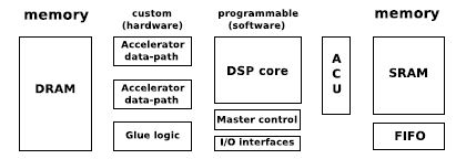
Figure 1.1, taken from [CAT 98b], shows that data transfers and memory access operations consume much more power than a data-path operation in both cases: hardware and software implementations. In the context of a typical heterogeneous system architecture, which is illustrated in Figure 1.2 (taken from [CAT 98b]), this architecture disposes of custom hardware, programmable software and a distributed memory organization that is frequently costly in terms of power and area. We can estimate that downloading an operand from off-chip memory for a multiplication consumes approximately 33 times more power than the multiplication itself for the hardware processor. Hence, in the case of a multiplication with two factors where the result is stored in the off-chip memory, the power consumption of transferring data is approximately 100 times more than the actual computation.
Figure 1.1. Dominance of transfer and storage over data-path operation both in Hardware and Software
Furthermore, studies presented in [CAT 94], [MEN 95], [NAC 96], [TIW 94] and [GON 96] confirm that data transfer and storage dominates power consumption for data-dominated applications in hardware and software implementations.
In the context of memory organization design, there are two strategies for minimizing the power consumption in embedded systems. The first strategy is to reduce the energy consumed in accessing memories. This takes a dominant proportion of the energy budget of an embedded system for data-dominated applications. The second strategy is to minimize the amount of energy consumed when information is exchanged between the processor and the memory. It reduces the amount of required processor-to-memory communication bandwidth [MAC 05].
Figure 1.2. Typical heterogeneous embedded architecture
It is clear that memory management has an impact on important cost metrics: area, performance and power consumption. In fact, the processor cores begin to push the limits of high performance, and the gap between processor and memory widens and usually becomes the bottleneck in achieving high performance. Hence, the designers of embedded systems have to carefully pay attention to minimize memory requirements, improve memory throughput and limit the power consumption by the system’s memory. Thus, the designer attempts to minimize memory requirements with the aim of lowering overall system costs.
We distinguish three problems concerning memory management and data assignment. The first problem is software oriented and aims at optimizing application code source regardless of the architecture; it is called a software optimization and it is presented in section 1.3.1. In the second problem, the electronic designer searches for the best architecture in terms of cost metrics for a specific embedded application. This problem is described in section 1.3.2. In the third problem, the designer is concerned with binding the application data into memory in a fixed architecture so as to minimize power consumption. This problem is presented in section 1.3.3.
We present some global optimizations that are independent of the target architectural platform; readers interested in more details about this are refereed to [PAN 01b]. These optimization techniques take the form of source-to-source code transformations. This has a positive effect on the area consumption by reducing the amount of data transfers and/or the amount of data to be stored. Software optimization often improves performances cost and power consumption, but not always. They are important in finding the best alternatives in higher levels of the embedded system design.
Code-rewriting techniques consist of loop and data-flow transformations with the aim of reducing the required amount of data transfer and storage, and improving access behavior [CAT 01]. The goal of global data-flow transformation is to reduce the number of bottlenecks in the algorithm and remove access redundancy in the data flow. This consists of avoiding unnecessary copies of data, modifying computation order, shifting of “delay lines” through the algorithm to reduce the storage requirements and recomputing issues to reduce the number of transfers and storage size [CAT 98a]. Basically, global loop and control-flow transformations increase the locality and regularity of the code’s accesses. This is clearly good for memory size (area) and memory accesses (power) [FRA 94] but of course also for performance [MAS 99]. In addition, global loop and control-flow transformations reduce the global life-times of the variables. This removes system-level copy overhead in buffers and enables storing data in smaller memories closer to the data paths [DEG 95, KOL 94].
The hierarchical memory organization is a memory optimization technique (see [BEN 00c] for a list of references). It reduces memory energy by exploiting the non-uniformities in access frequencies to instructions and data [HEN 07]. This technique consists of placing frequently accessed data into small energy-efficient memories, while rarely accessed information is stored in large memories with high cost per access. The energy cost of accessing and communicating with the small memories is much smaller than the cost required to fetch and store information in large memories [BEN 00a, CUP 98].
A good way for decreasing the memory traffic, as well as memory energy, is to compress the information transmitted between two levels of memory hierarchy [MAC 05]. This technique consists of choosing the set of data elements to be compressed/decompressed and the time instants during execution at which these compressions or decompressions should be performed [OZT 09]. The memory bottlenecks are mainly due to the increasing code complexity of embedded applications and the exponential increase in the amount of data to manipulate. Hence, reducing the memory-space occupancy of embedded applications is very important. For this reason, designers and researchers have devised techniques for improving the code density (code compression), in terms of speed, area and energy [BAJ 97]. Data compression techniques have been introduced in [BEN 02a, BEN 02b].
Ordering and bandwidth optimization guarantees that the real-time constraints are presented with a minimal memory bandwidth-related costs. Also, this determines which data should be made simultaneously accessible in the memory architecture.
Moreover, storage-bandwidth optimization takes into account the effect on power dissipation. The data that are dominant in terms of power consumption are split into smaller pieces of data. Indeed, allocating more and smaller memories usually results in less power consumption; but the use of this technique is limited by the additional costs generated by routing overheads, extra design effort and more extensive testing in the design [SLO 97].
This chapter does not cover optimization techniques on source code transformation. It is focused on optimization techniques on hardware and on data binding in an existing memory architecture.
We now present some techniques for optimizing the memory architecture design of embedded systems.
The goal of memory allocation and data assignment is to determine an optimal memory architecture for data structures of a specific application. This decides the memory parameters, such as the number and the capacity of memories and the number of ports in each memory. Different choices can lead to solutions with a very different cost, which emphasize how important these choices are. The freedom of the memory architecture is constrained by the requirements of the application. Allocating more or less memories has an effect on the chip area and on the energy consumption of the memory architecture. Large memories consume more energy per access than small memories, because of longer word – and bit – lines. So the energy consumed by a single large memory containing all the data is much larger than when the data are distributed over several smaller memories. Moreover, the area of a single memory solution is often higher when different arrays have different bit widths [PAN 01b].
For convenience and with the aim of producing sophisticated solutions, memory allocation and assignment is subdivided into two subproblems (a systematic technique has been published for the two subproblems in [SLO 97], [CAT 98c] and [LIP 93]). The first subproblem consists of fixing the number of memories and the type of each of them. The term “type” includes the number of access ports of the memory, whether it is an on-chip or an off-chip memory. The second subproblem decides in which of the allocated memories each of the application’s array (data) will be stored. Hence, the dimensions of the memories are determined by the characteristics of the data assigned to each memory and it is possible to estimate the memory cost. The cost of memory architecture depends on the word-length (bits) and the number of words of each memory, and the number of times each of the memories is accessed. Using this cost estimation, it is possible to explore different alternative assignment schemes and select the best one for implementation [CAT 98b]. The search space can be explored using either a greedy constructive heuristic or a full-search branch and bound approach [CAT 98b]. For small applications, branch and bound method and integer linear programming (ILP) find optimal solutions, but if the size of the application gets larger, these algorithms take a huge computation time to generate an optimal solution.
For one-port (write/read) memories, memory allocation and assignment problems can be modeled as a vertex coloring problem [GAR 79]. In this conflict graph, a variable is represented by a vertex, a memory is represented by a color and an edge is present between two conflicting variables. Thus, the variable of the application is “colored” with the memories to which they are assigned. Two variables in conflict cannot have the same color [CAT 98b]. This model is also used for assigning scalars to registers. With multi port memories, the conflict graph has to be extended with loops and hyperedges and an ordinary coloring is not valid anymore.
The objective of in-place mapping optimization is to find the optimal placement of the data inside the memories such that the required memory capacity is minimal [DEG 97, VER 91]. The goal of this strategy is to reuse memory location as much as possible and hence reduce the storage size requirements. This means that several data entities can be stored at the same location at different times. There are two subproblems: the intra-array storage and inter-array storage [CAT 98b]. The intra-array storage refers to the internal organization of an array in memory [LUI 07b, TRO 02]. The inter-array storage refers to the relative position of different arrays in memory [LUI 07a]. Balasa et al. [BAL 08] give a tutorial overview on the existing techniques for the evaluation of the data memory size.
A data transfer and storage exploration methodology is a technique for simultaneous optimization of memory architecture and access patterns. It has also been proposed for the case of data-dominated applications (e.g.multimedia devices) and network component applications (e.g. Automated Teller Machine applications) [CAT 98b, BRO 00, CAT 94, CAT 98a, WUY 96]. The goal of this methodology is to determine an optimal execution order for the data transfer and an optimal memory architecture for storing the data of a given application. The steps in this methodology are decoupled and placed in a specific order, which reduces the number of iterations between the steps and shortens the overall design time. These steps are:
The first three steps refer to architecture-independent optimizations; that is optimizations of the form of source-to-source code transformations. If these transformations are not applied, the resulting memory allocation is very likely far from optimal. The remaining stages consist of optimization techniques that address target memory architecture.
Memory partitioning has demonstrated very good potential for energy savings (in [MAC 05], a survey of effective memory partitioning approaches is presented). The basic idea of this method is to subdivide the address space into several smaller blocks and to map these blocks to different physical memory banks that can be independently enabled and disabled [FAR 95].
Incorporating scratchpad memory (SPM) [PAN 00, PAN 99] in the memory architecture is another very popular technique in memory management for reducing energy consumption. A scratchpad is a high-speed internal memory used for temporary storage of calculations, data and other work in progress. There are many works on this topic, for instance [CHO 09], [KAN 05], [ANG 05], [RAM 05], [PAN 97b], [PAN 97a] and [EGG 08]. An SPM is a high-speed internal memory that is used to hold small items of data for rapid retrieval. In fact, both the cache and SPM are usually used to store data, because accessing to the off-chip memory requires a relatively longer time [PAN 01a]. The memory is partitioned into data cache and SPM to exploit data reusability of multimedia applications [SIN 03].
Methods on using SPMs for data accesses are either static or dynamic. Static methods [BAN 02, VRE 03, AVI 02, STE 02] determine which memory objects (data or instructions) may be located in SPM at compilation time, and the decision is made during the execution of the program. Static approaches generally use greedy strategies to determine which variables to place in SPM, or formulate the problem as an ILP program or a knapsack problem to find an optimal allocation. Recently in [AOU 10a], [AOU 10b], [AOU 10e], [AOU 10d], [AOU 10c] and [IDO 10], operation research techniques (e.g. tabu search, and genetic and hybrid heuristic) have been proposed for this problem. Dynamic SPM allocation places data into the SPM, taking into account the latency variations across the different SPM lines [CHO 09, VER 04, ISS 07, FRA 04].
In memory allocation for high-level synthesis, the application addressed involves a relatively small number of signals4. Thus, techniques for dealing with the memory allocation are scalar oriented and use a scheduling phase ([SCH 92, STO 92, BAL 07]). Therefore, the major goal is typically to minimize the number of registers for storing scalars. This optimization problem is called register allocation [GAJ 92].
ILP formulations [SCH 92, BAL 88], line packing [KUR 87, HUA 09], graph coloring [STO 92] and clique partitioning techniques [TSE 86] have been proposed for register allocation. One of the first techniques, a graph coloring-based heuristic, is reported in [CHA 04]. It is based upon the fact that minimizing the number of registers is equivalent to the graph coloring problem. A graph is constructed for illustrating this problem. Vertices represent variables, edges indicate the interference (conflict) between variables and each color represents a different physical register. Many other variants of this coloring problem for register allocation have been proposed (e.g. see [BLA 10, ZEI 04, KOE 06]). More and more metaheuristic methods are used to find good solutions to this problem (e.g. see [SHE 07, TOP 07, MAH 09]). General approaches have been proposed for this problem (e.g. see [GRU 07, KOE 09, PER 08, PIN 93, CUT 08]).
We are only interested in the optimization techniques for memory architecture involving one-port memories. Consequently, the other techniques using multi-port or scratchpad are not addressed in this chapter.
This section presents some references for the data binding problem, which is to allocate data structure from a given application to a given memory architecture. Because of the provided architecture, the constraints considered and the criterion to optimize, there is a wide range of data binding problems.
First, we introduce some interesting works about the memory partitioning problem for low energy. Next, we present the works that take into account the number and capacities of memory banks, and the number of accesses to variables. Finally, we discuss other works that consider the aforementioned constraints and use an external memory.
These works have similarities with the last three versions of the memory allocation problem addressed in Chapters 3, 4 and 5. A fixed number of memory banks is the main feature that they have in common. The two more complex versions of the memory allocation problem consider the memory bank capacities, the number of accesses to variables and the use of an external memory.
Section 1.3.1 introduced the memory partitioning problem, which is a typical performance-oriented solution, and energy may be reduced only for some specific access patterns. In contrast, the memory partitioning problem for low energy reduces the energy for accessing memories [BEN 02c]. The main characteristics of this problem are the fixed number of memory banks and the ability of independently accessing the memory banks.
There are some techniques to address the memory partitioning problem for low energy, and some different versions of this problem depending on the considered architecture.
In [KOR 04], a method for memory allocation and assignment is proposed using multi-way partitioning, but the partitioning algorithm to resolve the conflicts in the conflict graph is not described. In [KHA 09], a min-cut partitioning algorithm, initially proposed in [SHI 93], is used for memory allocation and assignment. To apply this algorithm, the conflict graph is needed and the designer must set a number of partitions (i.e. the number of memory banks). Moreover, the min-cut algorithm tends to find minimum cuts in the conflict graph, resolving minimum conflicts only. The conflict graph is modified so as to maximize the cuts. Maximizing the cut results in resolving the maximum number of conflicts in the conflict graph.
In [BEN 00b], Benini et al. propose a recursive algorithm for the automatic partitioning of on-chip memory into multiple banks that can be independently accessed. The partitioning is carried out according to the memory access profile of an embedded application, and the algorithm is constrained to the maximum number of banks.
In [CON 09], Cong et al. present a memory partitioning technique to improve throughput and reduce energy consumption for given throughput constraints and platform requirement. This technique uses a branch and bound algorithm to search for the best combination of partitions.
Sipkovà [SIP 03] addresses the problem of variable allocation to a dual memory bank, which is formulated as the max-cut problem on an interference graph. In an interference graph, each variable is represented by a vertex, an edge between two vertices indicates that they may be accessed in parallel, and that the corresponding variables should be stored in separate memory banks. Thus, the goal is to partition the interference graph into two sets in such a way that the potential parallelism is maximized, that is the sum of the weights of all edges that connect the two sets is maximal. Several approximating algorithms are proposed for this problem. Furthermore, [MUR 08] presents an integer linear program and a partitioning algorithm based on coloring techniques for the same problem.
The work presented in [SHY 07] takes into account memory bank capacities, sizes and the number of accesses to variables for addressing the problem of reducing the number of simultaneously active memory banks, so that the other memory banks that are inactive can be put to low-power modes to reduce energy consumption. The considered architecture has multiple memory banks and various low-power operating modes for each of these banks. This problem is modeled like a multi-way graph partitioning problem, and well-known heuristics are used to address it [SHY 07].
A recent work that also considers the capacity constraints, sizes and the number of accesses is presented in [ZHA 11]. This paper proposes an ILP model to optimize the performance and energy consumption of multi-module memories by solving variable assignment, instruction scheduling and operating mode setting problems simultaneously. Thus, this model simultaneously addresses two problems: instruction scheduling and variable assignment. Two methods are presented for solving the proposed ILP model. The first method is a linear programming (LP)-relaxation to reduce the solution time, but it gives only lower bounds to the problem. The second method is a variable neighborhood search (VNS), which drastically reduces the computation time without sacrificing much to the solution quality.
Some heuristics to solve a buffer allocation problem applicable to explicitly parallel architectures are proposed in [MAR 03]. This problem is related to the multi-way constrained partitioning problem. Here, each partition is a set of buffers accessed in parallel and the number of buffers in each partition is less than or equal to the number of memory banks. The list of partitions is periodically executed. A set of memory banks of a fixed capacity is given. Thus, the objective is to compute an assignment of each buffer to a memory bank so as to minimize memory bank transfer overheads. All buffers have to be assigned and the buffers in the same partition are assigned to distinct memory banks.
In most cases, a processor requires one or more large external memories to store the long-term data (mostly of the DRAM type). In the past, the presence of these external memories in the architecture increased the total system power requirements. However, now these memories improve the throughput, but they do not improve the latency [NAC 01]. Some works that use an external memory are presented below.
Kumar, et al. [KUM 07] present a memory architecture exploration framework that integrates memory customization, which is logical to physical memory mapping and data layout. For memory architecture exploration, a genetic algorithm approach is used, and for the data layout problem, a heuristic method is proposed. This heuristic is used to solve the data allocation problem for all memory architectures considered in the exploration phase, which could be in several thousands. Hence, the heuristic must consider each architecture (on-chip memory size, the number and size of each memory bank, the number of memory ports per bank, the types of memory, scratchpad, RAM or cache) to perform the data allocation.
This heuristic starts considering the critical data (i.e. the data that have high access frequency) for designing an initial solution. Then, it backtracks to find changes in the allocation of data, which can improve the solution. These changes are performed considering the data size, and the minimum allocation cost of data in the memory bank.
Hence, the first step to build the initial solution is to identify and place all the critical data in the internal memory and the remaining data in the external memory. In the second step, the algorithm tries to resolve as many conflicts as possible (self-conflicts and parallel-conflicts) by using the different dual/single access memory banks. The data that are on self-conflict are first allocated and then the data on critical parallel-conflict. The metaheuristic first uses the dual-access memory bank to allocate data; the single-access memory banks are used only when the all dual-access memory banks are full.
Corvino et al. [COR 10] present a method to map data parallel applications into a specific hardware accelerator. Data parallel applications are executed in a synchronous architectural model. Initially, the data to be processed are stored in the external memory, and during the cycles of application, the manipulated data can be stored in local memories.
The general idea of the proposed method is to mask the times to transfer data with the time to perform computations. A method based on an integer partition is used to reduce the exploration space.
Most of the works presented in this section do not provide a mathematical model and a comparison with an exact method. Moreover, their proposed approaches are only tested on a single instance. In this work, we propose a formal mathematical model for each version of the memory allocation problem. Additionally, the proposed metaheuristics are compared with exact approaches on a large set of instances.
No version of memory allocation problem is totally concerned with the architecture, constraints and/or the criterion to optimize the problems presented in this section.
This section is inspired from the works of the CNRS GDR-RO working group “Problématiques d’optimisation discrete en micro-électronique” [MAR 10a, MAR 10b, KIE 11].
In the last decades, researchers and practitioners of electronics have revealed needs for further optimizations. Additionally, even “old” problems have become more challenging due to the larger instances and increasing complexity of the architecture.
However, the complexity, size and novelty of problems encountered in microelectronics make this area a source of exciting and original optimization problems for the community of operations research (OR). Indeed, the models and data are complex and poorly formalized, and problems are often very challenging. Furthermore, the integration of more components on the circuit reveals new and/or large-size problems to model and solve.
These are the reasons why a new discipline has appeared at the border of operations research and electronics. This discipline is concerned with addressing electronic problems using operations research methods. Isolated experiments have first been reported, which explain both the heterogeneity in the electronic topics addressed, and the great diversity in the operations research methods used to solve them. The following paragraphs mention some examples of OR methods used for addressing electronics problems.
The development of modern algorithms for the placement problem is one of the oldest applications of OR to microelectronics. This problem consists of placing the elements of a circuit in the target area so that no elements overlap with each other, and the total length of interconnections is minimized. The circuits may have billions of transistors, and five times more connections. A team in Bonn, led by Bernhard Korte and Jens Vygen, work on this problem in collaboration with IBM. They develop combinatorial optimization methods [KOR 08], which are implemented in their solver called “Bonn Tools” [BRE 08]. Futhermore, [CHA 09] summarizes the algorithms implemented for this problem, which are mainly based on simulated annealing, min-cut and analytical placement basics.
Another well-known example of OR for electronics is the implementation of metaheuristics for the register allocation problem [SHE 07, TOP 07, MAH 09, BLA 10, ZEI 04, KOE 06, GRU 07, PER 08]), as mentioned in section 1.3.2.
Advanced metaheuristics have been designed for high-level synthesis tools [TRA 10, COU 09, TRA 08, SEV 11, ROS 08]. They are considered to be efficient approaches, and some of them have been implemented in the high-level synthesis platform, [GAU 93].
Many metaheuristics have been developed for the management of scratchpad memories ([AOU 10a, AOU 10b, AOU 10e, AOU 10d, AOU 10c, IDO 10]), and management of system on-chip ([DAF 08, CRÉ 10, KOR 04, DU 08]), as mentioned in section 1.3.2.
Some OR methods have been applied for evaluating communication processors [SEN 09], for very large scale integration (VLSI) [PEY 09], for improving the performance of ASICs chips [HEL 03] and for the memory architecture exploration [KUM 07, ZHA 11].
There is not a single scientific object of interest in the activity of operations research for electronics, and the operational researcher usually faces the following issues when entering the electronics field.
Similarly, for electronic practitioners, entering into the OR field requires an adaptation time. Hence, the electronic practitioners, who design the conception tools, often develop their own heuristics, which are often considered poor by OR standards.
1 Creeping elegance is the tendency of programmers to disproportionately emphasize elegance in software at the expense of other requirements such as functionality, shipping schedule and usability.
2 Data-dominated applications are so named like this because they process enormous amounts of data.
3 Data-path is a collection of functional units, such as arithmetic logic units or multipliers, that perform data processing operations. A functional unit is a part of a central processing unit (CPU) that performs the operations and calculations called by the computer program.
4 In literature, the term “signal” is often used to indicate an array as well.