CHAPTER 6
Unit ELEC3/008
Principles of electrical science

Learning outcomes
When you have completed this chapter you should:
1. Understand the mathematical methods that are appropriate to electrical science and principles.
2. Understand the principles of electronic components and devices in electrotechnical systems.
3. Understand the principles of alternating current circuits.
4. Understand the principles and applications of luminaires.
5. Understand the principles and applications of direct current machines and alternating current motors.
6. Understand the operating principles of electrical components.
7. Understand the principles of electric heating.
Assessment criteria 1.1
Apply mathematical methods relevant to electrical science and principles
Mathematics is used in many different engineering applications but are underpinned through certain conventions, which are not always signposted. For instance, all numbers tend to be positive unless otherwise stated. The number 5 for example is actually positive otherwise it would be shown as −5. In fact, it can also be represented as 5/1 but we tend not to indicate the numerator in normal convention. There are other mathematical conventions used when adding or subtracting numbers. For example:
like signs add: unlike signs subtract
The same applies when multiplying and dividing, like signs show a positive results, unlike signs a negative one. This applies when you multiply two negative numbers.
Bodmas
BODMAS is a classic mathematical convention and very important especially since modern day calculators automatically apply the rules surrounding BODMAS, which means that its reasoning is sometimes lost.
In my experience this is shown when applicants are given a basic mathematical test when taking part in an interview process and candidates appear horrified that calculators are not permitted.
BODMAS stands for:
B: Brackets
O: Other operation such as indices
D: Division
M: Multiplication
A: Addition
S: Subtraction
Because the other function is mostly indices, it is sometimes referred to as BIDMAS.
Try to solve the following example:
Some readers might conclude that the answer is 20, since they would apply the logic of 6 + 4 =10 × 2 = 20.
Unfortunately, BODMAS dictates that multiplying comes before adding, which means that the answer is 4 × 2 = 8 + 6 = 14.
BODMAS is applied to equations by working out brackets inside initially, before multiplying them out. Other means applying indices such as 33, which remember actually works out as 3 × 3 × 3 = 27. The remainder would follow as directed through their function of: dividing, multiplying, adding, and subtracting. However, be aware that when only addition and subtraction remain then the equation should be processed from left to right.
Let’s take the following example:
Work out the brackets inside first (10 – 8)2 becomes
Next, multiply the brackets out, which includes indices: 4 × 22 = 4 × 4 = 16
Which leaves us with:
Next, any multiplication 2 × 4 = 8 and 5 × 16 = 80
now addition
Try the next example:
If your answer is 68, then you have forgotten that when only + and – remain, then the equation should be processed from left to right.
The answer should be 72.
Percentages
Percentages are based on a fraction but are then multiplied by 100 to show it as a percentage.
For example, if a student gets 42 correct answers out of a total of 48 questions in an exam how can we work this out as a percentage (%)?
If we now multiply by 100, we will change the answer into a percentage (%).
A very important stage in designing an electrical circuit is to ensure that it is not too long, and this is known as confirming volt drop requirements. Both power and lighting circuits are permitted a certain percentage of voltage drop which is lost across the resistance of its conductors, but excessive amounts robs electrical loads of working voltage. This can then manifest in problems such as electrical motors operating slowly or lights appearing dim. The wiring regulations BS 7671 specify that lighting and power circuits must operate within 3% and 5% respectively. If these percentages are not met, then the cross sectional area of the cable must be increased.
When applying these volt drop tolerances to a domestic single phase supply the maximum voltage that can be dropped across a lighting circuit is:
Power circuits are permitted
Powers of 10
Engineering make great use of applied mathematics such as powers of 10, a system of numbers that is arrived at by multiplying the number 10 by itself a number of times. Such numbers include:
It is very easy to multiply and divide any multiple of 10 by following a simple rule.
For example:
1000 × 1000 = 1000000 (when multiplying, simply combine the total number of zeros)
When dividing, cancel out the number of zeros in the denominator with respect to the numerator
We also relate powers of 10 to what is known as scientific notation, therefore 3000 can be expressed as: 3 × 10³ and 3000000 as 3 × 10⁶ accordingly.
We can also express these types of numbers through some common prefixes as can be seen from the table below. For instance 3000 V or 3 000 000 V would be written as 3 kV and 3 MV respectively.
Fractions
To consider fractions think of a cake.
Cut into two, each part is a half
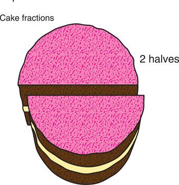
Figure 6.1 Fractions can be considered as breaking or dividing something into equal parts. The simplest is two halves.
Adding fractions
When adding fractions we form what is called a common denominator: a number that is divisible (go into) to both sides.
For example
is the common denominator, because both 4 goes into itself once and 2 goes into 4 twice
Then simplify by adding both numerators.
Subtraction follows the same procedure, simplifying by taking away both elements at the end.
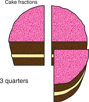
Figure 6.2 If you eat one quarter (1/4) of the cake, then you are left with three quarters (3/4) or 3 slices.
Multiplying fractions
Simply multiply all the top numbers and all the bottom numbers.
We can simplify the answer by working out how many times 4 goes into 32.
Dividing fractions
A very useful rule when dividing fractions is to invert the fraction on the right. Therefore
Then treat the fraction the same as you would when multiplying.
Algebra
In algebra another mathematical convention exists in that the multiplication sign is not always shown but must be applied to the letters or values involved. For instance, F = B I L is a formula regarding electrical motors but the relationship between B I L is actually B × I × L. The rule to remember here is that a lack of a + or − sign in a cluster of elements signifies that they should be multiplied.
The letters represent values which if known can be substituted to find the amount of force that the motor produces.
We also carry over some previous BODMAS rules, such as multiplication before addition or subtraction.
For example
Laws of indices
Large numbers can be represented by indices.
For instance: 23 is actually 2 × 2 × 2 = 8
The number 2 is known as the base and the number 3 the index and certain rules can be applied but only to numbers using the same base.
To multiply indices with the same base, add the indices.
When dividing indices with the same base, subtract the indices.
Remember, these rules only apply to indices that share the same base number.
Another rule that can help to factorize is an equation which is the reverse of the Lowest Common Factor used in fractions and is known as the Highest Common Factor (HCF) of the numbers involved. For example, in order to factorize the following equation: 27a + 18
The highest HCF that applies to both numbers is 9 because it applies to 27 (3 × 9 = 27) and 18 (9 × 2 = 18).
This means that our equation becomes
Trigonometry
A Greek mathematician called Pythagoras found that if we know the length of two of sides, we can work out the length of the other.
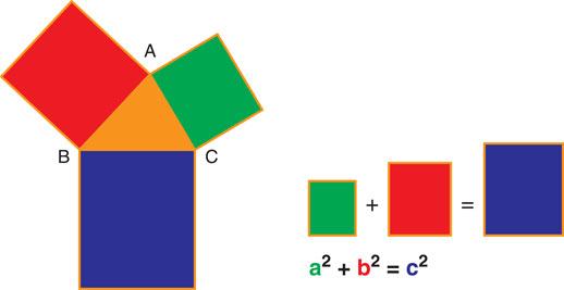
Figure 6.3 The area of a + b = c.
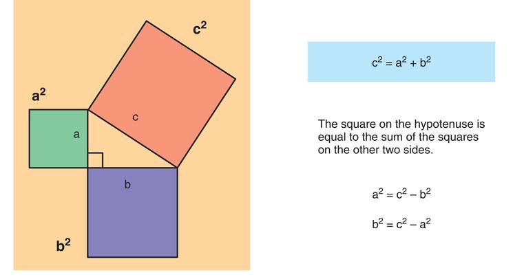
Figure 6.4 By using transposition of formula we can determine .
Using the rules of transposition any of the mathematical relationships can be found if at least two sides are known.
The sides are labelled hypotenuse, opposite and adjacent and, while students are exposed to this theorem in school, in electrical installation it is used to indicate and correct power factor issues which are brought about when inductors cause a circuit’s current to lag the voltage.
The example given below shows how the length of the hypotenuse (C) can be found because we know the values of the other two sides.
To calculate the angle, however, we need to use trigonometry principles and the relationship between sine, cosine and tangent.
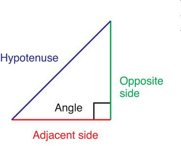
Figure 6.5 Although the hypotenuse is the longest side, it can also be recognised as the side which is opposite the right angle.
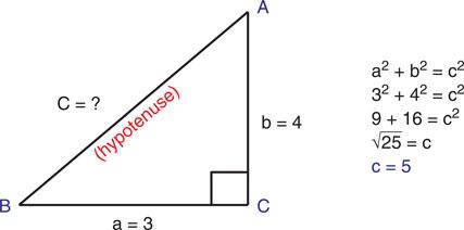
Figure 6.6 An example of a right sided triangle whose sides form a ratio of 3:4:5.
A famous acronym used to remember these relationships in the form of a formula is: SOH CAH TOA. In other words:
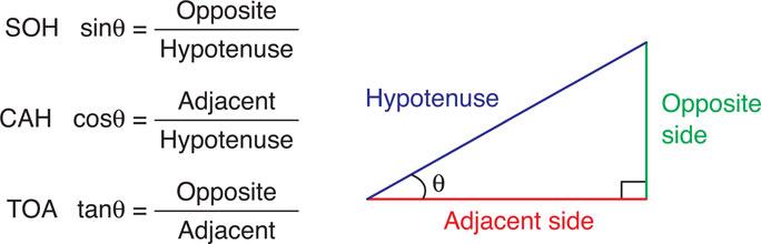
Figure 6.7 If we know two sides of a right angled triangle, we can calculate the unknown side as well as the angle between them.
Referring to the aircraft, we can find the angle of its elevation because again we know two of its sides, adjacent (400) and opposite (300). The trigonometry relationships that involves the adjacent and the opposite is tangent (TOA). Our formula therefore becomes
To obtain the actual angle in degrees we use the inverse function of tan: 0.75 tan−¹ = 36.869° (36.7°)
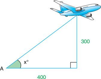
Figure 6.8 Opposite and adjacent are known, therefore we use tangent the function, TOA = opposite/adjacent.
Triangles
The right-sided triangle has already been covered through Pythagoras’ theorem but others exist such as shown below:

Figure 6.9 Equilateral, Isosceles and Scalene triangles.
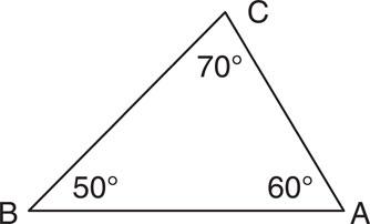
Figure 6.10 The three interior angles of a triangle always add up to 180°.
Their respective properties are as follows:
• Equilateral: all angles are 60° and sides are equal in sides.
• Isosceles: has two equal sides and the angles opposite these sides are also equal.
• Scalene: a triangle with no equal sides or equal angles.
All angles within a triangle add up to 180°.
Work out the unknown angle from the example below:
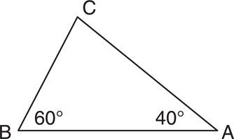
Figure 6.11 60° + 40° – 180° = 80°.
Transposion of formula
There are many different ways of transposing a formula but the simplest makes use of the OPPOSITE RULE. For instance:
 Definition
Transposition of formula using the opposite rule
Add = Subtract
Multiply = Divide
x2 Raise to the power = Square root
1 The opposite of Addition is Subtraction
2 The opposite of Multiply is Divide
3 The opposite of Squaring is Square root
By way of an example we can see this below:
Rule number 1
(The opposite of Addition is Subtraction.)
Rule number 2
(The opposite of Multiply is Divide.)
In electrical installation and indeed engineering we tend not to use the symbol ÷ when we are showing a divide sign. Therefore 1 ÷ 2, is effectively ½ but written in an equation it would be:
Rule number 3
Revision: (The square root of a number is a value that, when multiplied by itself, gives that number. For example: 4 × 4 = 16, so the square root of 16 is 4.)
52 means 5 × 5, which equals 25.
The square root of 25 is 5.
(The opposite of Squaring is Square Root.)
The reason why the opposite rule works is that we can keep an equation or formula balanced by changing the opposite function.
Remember to keep an equation balanced, whatever you do to one side you must do the same or the opposite to the other side.
Let us work through a few examples in order to solve certain values.

Figure 6.12 To keep the balance correct within an equation changes on one side must also be made to the other.
Example 1
However, what if I need to re-arrange the formula to find c?
We do this by following three simple steps. Remember, the aim is to get c by itself.
Step 1: focus on the letter you want to find and write this down.
Step 2: Look which letter or value is already on its own, or in other words which letter or value is already on the other side of the = sign. In this case, d.
Step 3: Move the letter or value that is left away from the one you want to find. In this case the letter remaining is +a, which becomes −a as it moves across.
Example 2
Ohm’s law states that V = I × R.
However, what if I need to re-arrange the formula to find I?
Remember the aim is to get I by itself.
Step 1: focus on the letter you want to find and write this down.
Step 2: Look which letter or value is already on its own, or in other words which letter or value that is already on the other side of the = sign. In this case V.
Step 3: Move the letter or value that is left away from the one you want to find.
In this case the letter remaining is R, which is shown on top, which we therefore consider as multiply. The opposite of multiply is divide therefore simply move the R from the top of the equation to the bottom (underneath).
Example 3
Re-arrange the formula by transposing to find b.
Step 1: focus on the letter you want to find and write this down. Just for now we write b2 as we would if it was b.
Step 2: Look which letter or value is already on its own, or in other words which letter or value that is already on the other side of the = sign. In this case c.
Step 3: Move the letter or value that is left away from the one you want to find. In this example a2 becomes −a2. Therefore our equation becomes:
Last part coming up, we need to find b not b2. Therefore, using the opposite rule remove the 2from b, but keep the formula balanced by square-rooting the other side.
If we now work back in order to find c, the first thing we need to do is get rid of the square root sign, and we do this by squaring b.
We then follow the three steps.
Statistics
When calculating statistics the mean (or average) is the most popular and well known measurement. In the UK we know this value more as the average, but this can be confusing because the term median is also a measure of average but is calculated in a slightly different way.
For instance, in electrical installation if we used different values of insulation resistance obtained by testing several circuits then we can work out what the mean or median values are, but the usefulness or transparency of what these values represent largely depends on the actual data being measured or compared. Examine the following values:
Definition
Averages
The mean should be used to calculate average if the numbers are similar in size. If not, use the median.
To work out the mean I add up all the values and divide by the number of values, which is 9 in this case.
This gives me a mean value of = 46.9 MΩ
To work out the median I first have to put them in order:
Therefore:
Becomes:
Given that the sequence of numbers is odd (9) then the middle number will be the median, which is the fifth number = 2 MΩ.
But the question is which average is more accurate for representing the data being compared. On reflection, the data used were not symmetrical with a wide spectrum of values ranging from 0.5 to 300 MΩ. This means that the median gives a more accurate reflection of the true average because it sits in the middle of the data.
By the way, had the sequence of numbers been even as shown below with 12 values, then again having put them in order I would work out the median by taking the middle two values and dividing by two.
Becomes:
The other average that is sometimes used is the mode, which shows the most re-occurring value. In the above example this would be 300 MΩ since it showed up three times.
 Key fact
To be able to make calculations accurately and confidently are an important skill at this level in the electrical installation training course. I always recommend a good math book to my students called ‘Electrical Installation Calculations’: Advanced, Level 3. By Christopher Kitcher and A.J.Watkins.
Assessment criteria 2.1
Outline the operating principles of components and devices
Basic electronics
There are numerous types of electronic components – diodes, transistors, thyristors and integrated circuits (ICs) – each with its own limitations, characteristics and designed application. When repairing electronic circuits it is important to replace a damaged component with an identical or equivalent component. Manufacturers issue comprehensive catalogues with details of working voltage, current, power dissipation, etc., and the reference numbers of equivalent components. These catalogues of information, together with a high impedance multimeter, should form a part of the extended toolkit for anyone in the electrical industries proposing to repair electronic circuits.
Electronic circuit symbols
The British Standard BS EN 60617 recommends that particular graphical symbols should be used to represent a range of electronic components on circuit diagrams. The same British Standard recommends a range of symbols suitable for electrical installation circuits with which electricians will already be familiar. Figure 6.15 shows a selection of electronic symbols.
Resistors
All materials have some resistance to the flow of an electric current but, in general, the term resistor describes a conductor specially chosen for its resistive properties.
Resistors are the most commonly used electronic component and they are made in a variety of ways to suit the particular type of application. They are usually manufactured as either carbon composition or carbon film. In both cases the base resistive material is carbon and the general appearance is of a small cylinder with leads protruding from each end, as shown in Fig. 6.16(a). If subjected to overload, carbon resistors usually decrease in resistance since carbon has a negative temperature coefficient. This causes more current to flow through the resistor, so that the temperature rises and failure occurs, usually by fracturing. Carbon resistors have a power rating between 0.1 and 2 W, which should not be exceeded.
Definition
Resistors are used to limit the current in a circuit.
All materials have some resistance to the flow of an electric current, but, in general, the term resistor describes a conductor specially chosen for its resistive properties.
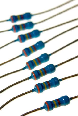
Figure 6.13 Resistors used in electrical circuits.

Figure 6.14 A rheostat is a resistor whose resistance can be changed in order to control circuit current.
When a resistor of a larger power rating is required a wire-wound resistor should be chosen. This consists of a resistance wire of known value wound on a small ceramic cylinder which is encapsulated in a vitreous enamel coating, as shown in Fig. 6.16(b). Wire-wound resistors are designed to run hot and have a power rating of up to 20 W. Care should be taken when mounting wire-wound resistors to prevent the high operating temperature affecting any surrounding components.
A variable resistor is one that can be varied continuously from a very low value to the full rated resistance. This characteristic is required in tuning circuits to adjust the signal or voltage level for brightness, volume or tone. The most common type used in electronic work has a circular carbon track contacted by a metal wiper arm. The wiper arm can be adjusted by means of an adjusting shaft (rotary type) or by placing a screwdriver in a slot (preset type), as shown in Fig. 6.17. Variable resistors are also known as potentiometers because they can be used to adjust the potential difference (voltage) in a circuit. The variation in resistance can be either a logarithmic or a linear scale.
The value of the resistor and the tolerance may be marked on the body of the component either by direct numerical indication or by using a standard colour code. The method used will depend upon the type, physical size and manufacturer’s preference, but in general the larger components have values marked directly on the body and the smaller components use the standard resistor colour code.
A rheostat, on the other hand, is a similar device but is used to control the current in a circuit.
Abbreviations used in electronics
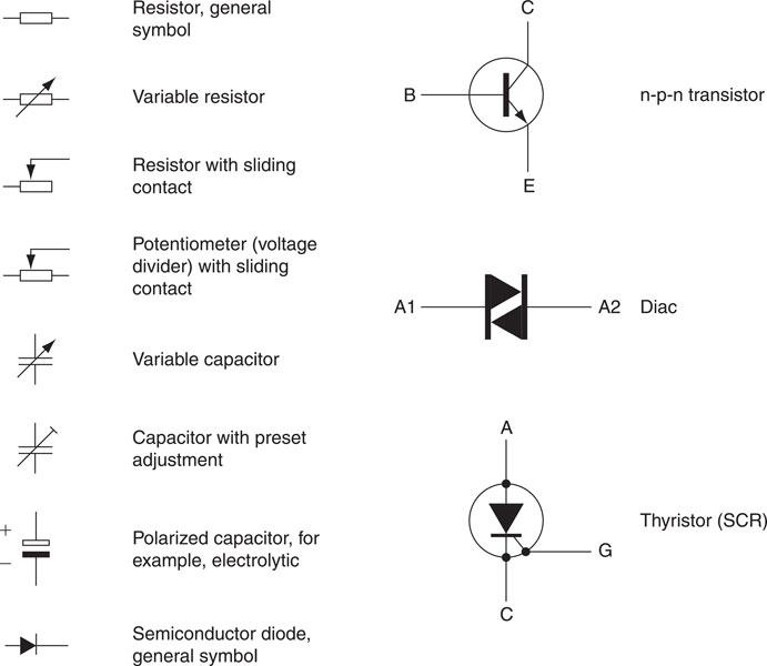
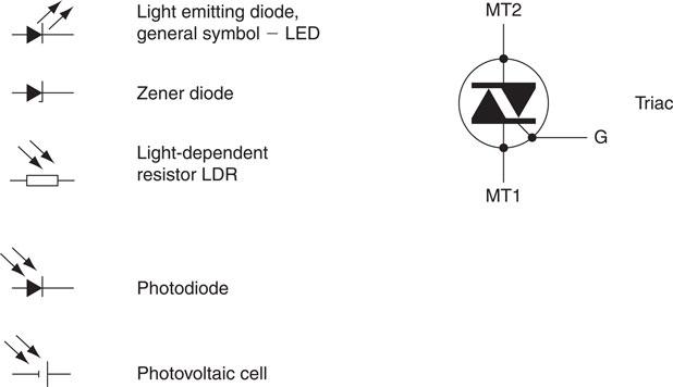
Figure 6.15 Some BS EN 60617 graphical symbols used in electronics.
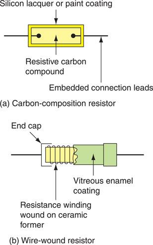
Figure 6.16 Construction of resistors.
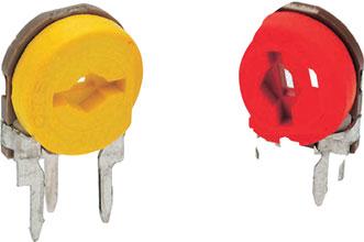
Figure 6.17 Types of variable resistors.
Where the numerical value of a component includes a decimal point, it is standard practice to include the prefix for the multiplication factor in place of the decimal point, to avoid accidental marks being mistaken for decimal points. Multiplication factors and especially factors of 10 have already been dealt with at the beginning of this chapter.
The abbreviation
Therefore, a 4.7 kΩ resistor would be abbreviated to 4 k7, a 5.6Ω resistor to 5R6 and a 6.8 MΩ resistor to 6 M8.
Tolerances may be indicated by adding a letter at the end of the printed code.
The abbreviation F means ±1%, G means ±2%, J means ±5%, K means ±10% and M means ±20%. Therefore a 4.7 kΩ resistor with a tolerance of 2% would be abbreviated to 4 k7G. A 5.6 Ω resistor with a tolerance of 5% would be abbreviated to 5R6J. A 6.8 MΩ resistor with a 10% tolerance would be abbreviated to 6 M8K.
This is the British Standard BS 1852 code, which is recommended for indicating the values of resistors on circuit diagrams and components when their physical size permits.
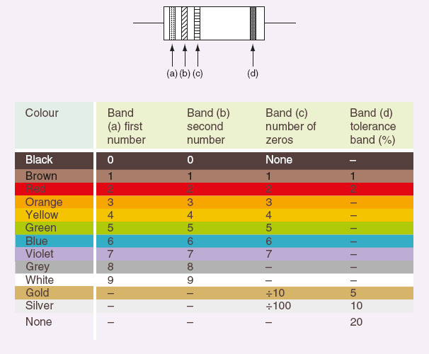
The standard colour code
Small resistors are marked with a series of coloured bands, as shown in Table 6.3. These are read according to the standard colour code to determine the resistance. The bands are located on the component towards one end. If the resistor is turned so that this end is towards the left, the bands are then read from left to right. Band (a) gives the first number of the component value, band (b) the second number, band (c) the number of zeros to be added after the first two numbers and band (d) the resistor tolerance. If the bands are not clearly oriented towards one end, first identify the tolerance band and turn the resistor so that this is towards the right before commencing to read the colour code as described.
The tolerance band indicates the maximum tolerance variation in the declared value of resistance. Thus a 100 Ω resistor with a 5% tolerance will have a value somewhere between 95 and 105 Ω, since 5% of 100 Ω is 5 Ω.
Table 6.3 The resistor colour code
Example 1
A resistor is colour coded yellow, violet, red, gold. Determine the value of the resistor.
Band (a) – yellow has a value of 4
Band (b) – violet has a value of 7
Band (c) – red has a value of 2
Band (d) – gold indicates a tolerance of 5%
The value is therefore 4700 ± 5%
This could be written as 4.7 kΩ ± 5% or 4 k7J.
Example 2
A resistor is colour coded green, blue, brown, silver. Determine the value of the resistor.
Band (a) – green has a value of 5
Band (b) – blue has a value of 6
Band (c) – brown has a value of 1
Band (d) – silver indicates a tolerance of 10%
The value is therefore 560 ± 10% and could be written as 560Ω ± 10% or 560 RK.
Example 3
A resistor is colour coded blue, grey, green, gold. Determine the value of the resistor.
Band (a) – blue has a value of 6
Band (b) – grey has a value of 8
Band (c) – green has a value of 5
Band (d) – gold indicates a tolerance of 5%
The value is therefore 6,800,000 ± 5% and could be written as 6.8 M Ω ± 5% or 6 M8J.
Example 4
A resistor is colour coded orange, white, silver, silver. Determine the value of the resistor.
Band (a) – orange has a value of 3
Band (b) – white has a value of 9
Band (c) – silver indicates divide by 100 in this band
Band (d) – silver indicates a tolerance of 10%
The value is therefore 0.39 ± 10% and could be written as 0.39 Ω ± 10% or R39 K.
 Try this
Electronics
Electricians are increasingly coming across electronic components and equipment. Make a list in the margin of some of the electronic components that you have come across at work.
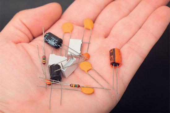
Figure 6.18 A handful of electronic resistors and capacitors.
Preferred values
It is difficult to manufacture small electronic resistors to exact values by mass production methods. This is not a disadvantage as in most electronic circuits the value of the resistors is not critical. Manufacturers produce a limited range of preferred resistance values rather than an overwhelming number of individual resistance values. Therefore, in electronics, we use the preferred value closest to the actual value required.
A resistor with a preferred value of 100 Ω and a 10% tolerance could have any value between 90 and 110 Ω. The next larger preferred value which would give the maximum possible range of resistance values without too much overlap would be 120 Ω. This could have any value between 108 and 132 Ω. Therefore, these two preferred value resistors cover all possible resistance values between 90 and 132 Ω. The next preferred value would be 150 Ω, then 180 Ω, 220 Ω and so on.
There is a series of preferred values for each tolerance level, as shown in Table 6.3, so that every possible numerical value is covered. Table 6.4 indicates the values between 10 and 100, but larger values can be obtained by multiplying these preferred values by some multiplication factor. Resistance values of 47 Ω, 470 Ω, 4.7 kΩ, 470 kΩ, 4.7 MΩ, etc., are available in this way.
Testing resistors
The resistor being tested should have a value close to the preferred value and within the tolerance stated by the manufacturer. To measure the resistance of a resistor which is not connected into a circuit, the leads of a suitable ohmmeter should be connected to each resistor connection lead and a reading obtained. If the resistor to be tested is connected into an electronic circuit it is always necessary to disconnect one lead from the circuit before the test leads are connected, otherwise the components in the circuit will provide parallel paths, and an incorrect reading will result.
Capacitors
In this section we shall consider the practical aspects associated with capacitors in electronic circuits.
A capacitor stores a small amount of electric charge; it can be thought of as a small rechargeable battery that can be quickly recharged. In electronics we are not only concerned with the amount of charge stored by the capacitor but in the way the value of the capacitor determines the performance of timers and oscillators by varying the time constant of a simple capacitor–resistor circuit.
Definition
Capacitance is the ability to store electrical charge.
Capacitors in action
If a test circuit is assembled as shown in Fig. 6.20 and the changeover switch connected to d.c., the signal lamp will only illuminate for a very short pulse as the capacitor charges. The charged capacitor then blocks any further d.c. current flow. If the changeover switch is then connected to a.c. the lamp will illuminate at full brilliance because the capacitor will charge and discharge continuously at the supply frequency. Current is apparently flowing through the capacitor because electrons are moving to and fro in the wires joining the capacitor plates to the a. c. supply.
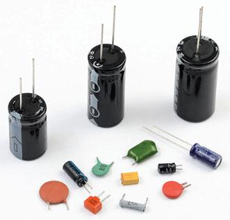
Figure 6.19 Capacitors come in several shapes and sizes.
Coupling and decoupling capacitors
Capacitors can be used to separate a.c. and d.c. in an electronic circuit. If the output from circuit A, shown in Fig. 6.21(a), contains both a.c. and d.c. but only an a.c. input is required for circuit B then a coupling capacitor is connected between them. This blocks the d.c. while offering a low reactance to the a.c. component. Alternatively, if it is required that only d.c. be connected to circuit B, shown in Fig. 6.21(b), a decoupling capacitor can be connected in parallel with circuit B. This will provide a low reactance path for the a.c. component of the supply and only d.c. will be presented to the input of B. This technique is used to filter out unwanted a.c. in, for example, d.c. power supplies.
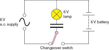
Figure 6.20 Test circuit showing capacitors in action.
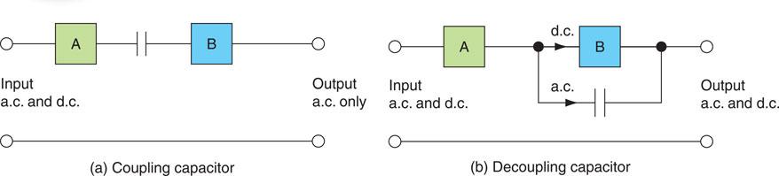
Figure 6.21 a) Coupling and (b) decoupling capacitors.
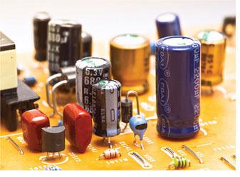
Figure 6.22 Capacitors, resistors and other components mounted on a circuit board.
Types of capacitor
There are two broad categories of capacitor, the non-polarized and polarized type. The non-polarized type can be connected either way round, but polarized capacitors must be connected to the polarity indicated otherwise a short circuit and consequent destruction of the capacitor will result. There are many different types of capacitor, each one being distinguished by the type of dielectric used in its construction. Figure 6.23 shows some of the capacitors used in electronics.
Polyester capacitors
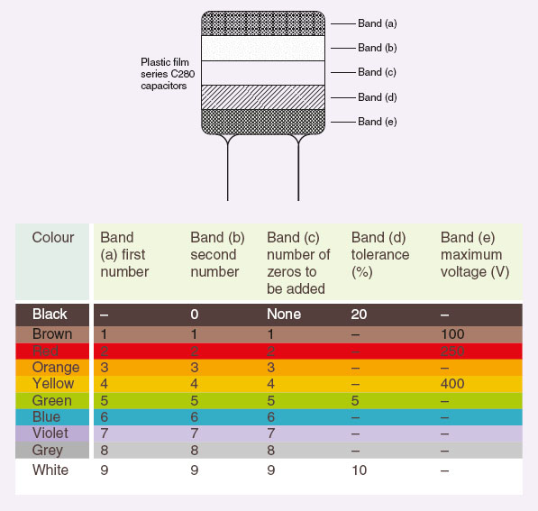
Polyester capacitors are an example of the plastic film capacitor. Polypropylene, polycarbonate and polystyrene capacitors are other types of plastic film capacitor. The capacitor value may be marked on the plastic film, or the capacitor colour code given in Table 6.5 may be used. This dielectric material gives a compact capacitor with good electrical and temperature characteristics. They are used in many electronic circuits, but are not suitable for high-frequency use.
Mica capacitors
Mica capacitors have excellent stability and are accurate to +1% of the marked value. Since costs usually increase with increased accuracy, they tend to be more expensive than plastic film capacitors. They are used where high stability is required, for example in tuned circuits and filters.

Figure 6.23 Capacitors and their symbols used in electronic circuits.
Table 6.5 Colour code for plastic film capacitors (values in picofarads)
Ceramic capacitors
Ceramic capacitors are mainly used in high-frequency circuits subjected to wide temperature variations. They have high stability and low loss.
Electrolytic capacitors
Electrolytic capacitors are used where a large value of capacitance coupled with a small physical size is required. They are constructed on the ‘Swiss roll’ principle as are the paper dielectric capacitors used for power-factor correction in electrical installation circuits. The electrolytic capacitors’ high capacitance for very small volume is derived from the extreme thinness of the dielectric coupled with a high dielectric strength. Electrolytic capacitors have a size gain of approximately 100 times over the equivalent non-electrolytic type. Their main disadvantage is that they are polarized and must be connected to the correct polarity in a circuit. Their large capacity makes them ideal as smoothing capacitors in power supplies.
 Safety first
Electrolytic capacitors are polarized, which means that one leg should be connected to the positive supply whilst the other to the negative and must never be cross connected.
Tantalum capacitors
Tantalum capacitors are a new type of electrolytic capacitor using tantalum and tantalum oxide to give a further capacitance/size advantage. They look like a ‘raindrop’ or ‘blob’ with two leads protruding from the bottom. The polarity and values may be marked on the capacitor, or a colour code may be used. The voltage ratings available tend to be low, as with all electrolytic capacitors. They are also extremely vulnerable to reverse voltages in excess of 0.3 V. This means that even when testing with an ohmmeter, extreme care must be taken to ensure correct polarity.
Variable capacitors
Variable capacitors are constructed so that one set of metal plates moves relative to another set of fixed metal plates as shown in Fig. 6.24. The plates are separated by air or sheet mica, which acts as a dielectric. Air dielectric variable capacitors are used to tune radio receivers to a chosen station, and small variable capacitors called trimmers or presets are used to make fine, infrequent adjustments to the capacitance of a circuit.
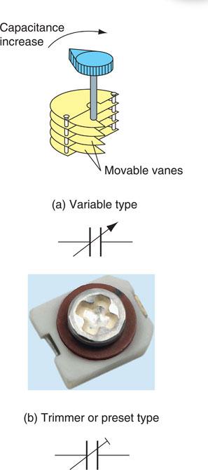
Figure 6.24 Variable capacitors and their symbols: (a) variable type; (b) trimmer or preset type.
Selecting a capacitor
When choosing a capacitor for a particular application, three factors must be considered: value, working voltage and leakage current. The unit of capacitance is the farad (symbol F), to commemorate the name of the English scientist Michael Faraday. However, for practical purposes the farad is much too large and in electrical installation work and electronics we use fractions of a farad as follows:
The power-factor correction capacitor used in a domestic fluorescent luminaire would typically have a value of 8μF at a working voltage of 400 V. In an electronic filter circuit a typical capacitor value might be 100 pF at 63 V.
One microfarad is one million times greater than one picofarad. It may be useful to remember that:
Safety first
You should never exceed a capacitor’s working voltage.
The working voltage of a capacitor is the maximum voltage that can be applied between the plates of the capacitor without breaking down the dielectric insulating material. This is a d.c. rating and, therefore, a capacitor with a 200 V rating must only be connected across a maximum of 200 V d.c. Since a.c. voltages are usually given as r.m.s. values, a 200 V a.c. supply would have a maximum value of about 283 V, which would damage the 200 V capacitor. When connecting a capacitor to the 230 V mains supply we must choose a working voltage of about 400 V because 230 V r.m.s. is approximately 325 V maximum. The ‘factor of safety’ is small and, therefore, the working voltage of the capacitor must not be exceeded.
An ideal capacitor that is isolated will remain charged forever, but in practice no dielectric insulating material is perfect, and the charge will slowly leak between the plates, gradually discharging the capacitor. The loss of charge by leakage through it should be very small for a practical capacitor.
Capacitor colour code
The actual value of a capacitor can be identified by using the colour codes given in Table 6.4 in the same way that the resistor colour code was applied to resistors.
Example 1
A plastic film capacitor is colour coded, from top to bottom, brown, black, yellow, black, red. Determine the value of the capacitor, its tolerance and working voltage.
From Table 6.5 we obtain the following:
Band (a) – brown has a value 1
Band (b) – black has a value 0
Band (c) – yellow indicates multiply by 10,000
Band (d) – black indicates 20%
Band (e) – red indicates 250 V
The capacitor has a value of 1,00,000 pF or 0.1 μF with a tolerance of 20% and a maximum working voltage of 250 V.
Example 2
Determine the value, tolerance and working voltage of a polyester capacitor colour-coded, from top to bottom, yellow, violet, yellow, white, yellow.
From Table 6.5 we obtain the following:
Band (a) – yellow has a value 4
Band (b) – violet has a value 7
Band (c) – yellow indicates multiply by 10,000
Band (d) – white indicates 10%
Band (e) – yellow indicates 400 V
The capacitor has a value of 4,70,000 pF or 0.47 μF with a tolerance of 10% and a maximum working voltage of 400 V.
Capacitance value codes
Where the numerical value of the capacitor includes a decimal point, it is standard practice to use the prefix for the multiplication factor in place of the decimal point. This is the same practice as we used earlier for resistors. The abbreviation μ means microfarad, n means nano farad and p means picofarad. Therefore, a 1.8 pF capacitor would be abbreviated to 1 p8, a 10 pF capacitor to 10 p, a 150 pF capacitor to 150 p or n15, a 2200 pF capacitor to 2n2 and a 10,000 pF capacitor to 10 n.
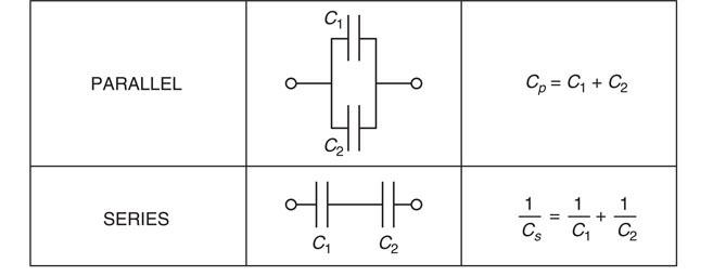
Figure 6.25 Capacitors in parallel are the same as resisters in series: you add up their values. Capacitors in series are equal to resistors in parallel: you add up their reciprocal values.
Semiconductor materials
Modern electronic devices use the semiconductor properties of materials such as silicon or germanium. The atoms of pure silicon or germanium are arranged in a lattice structure, as shown in Fig. 6.26. The outer electron orbits contain four electrons known as valence electrons. These electrons are all linked to other valence electrons from adjacent atoms, forming a covalent bond. There are no free electrons in pure silicon or germanium and, therefore, no conduction can take place unless the bonds are broken and the lattice framework is destroyed. To make conduction possible without destroying the crystal it is necessary to replace a four-valent atom with a three- or five-valent atom. This process is known as doping.
Definition
Electrical current is caused by the movement of negatively charged electrons which are attracted to a positive source.
If a three-valent atom is added to silicon or germanium a hole is left in the lattice framework. Since the material has lost a negative charge, the material becomes positive and is known as a p-type material (p for positive).
If a five-valent atom is added to silicon or germanium, only four of the valence electrons can form a bond and one electron becomes mobile or free to carry charge. Since the material has gained a negative charge it is known as an n-type material (n for negative).
Bringing together a p-type and n-type material allows current to flow in one direction only through the p–n junction. Such a junction is called a diode, since it is the semiconductor equivalent of the vacuum diode valve used by Fleming to rectify radio signals in 1904.
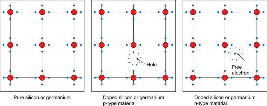
Figure 6.26 Semiconductor material.
Semiconductor diode
A semiconductor or junction diode consists of a p-type and n-type material formed in the same piece of silicon or germanium. The p-type material forms the anode and the n-type the cathode, as shown in Fig. 6.27. If the anode is made positive with respect to the cathode, the junction will have very little resistance and current will flow. This is referred to as forward bias. However, if reverse bias is applied, that is, the anode is made negative with respect to the cathode, the junction resistance is high and no current can flow, as shown in Fig. 6.28. The characteristics for a forward and reverse bias p–n junction are given in Fig. 6.29. It can be seen that a small voltage is required to forward bias the junction before a current can flow. This is approximately 0.6 V for silicon and 0.2 V for germanium. The reverse bias potential of silicon is about 1200 V and for germanium about 30 V. If the reverse bias voltage is exceeded the diode will break down and current will flow in both directions. Similarly, the diode will break down if the current rating is exceeded, because excessive heat will be generated. Manufacturers’ information therefore gives maximum voltage and current ratings for individual diodes which must not be exceeded. However, it is possible to connect a number of standard diodes in series or parallel, thereby sharing current or voltage, as shown in Fig. 6.30, so that the manufacturers’ maximum values are not exceeded by the circuit.
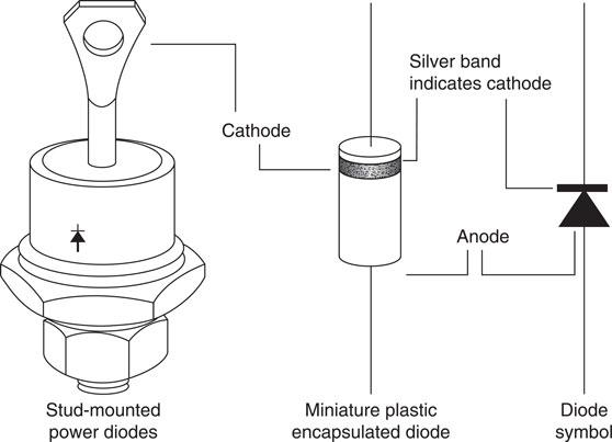
Figure 6.27 Symbol for and appearance of semiconductor diodes.
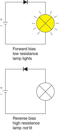
Figure 6.28 Forward and reverse bias of a diode.
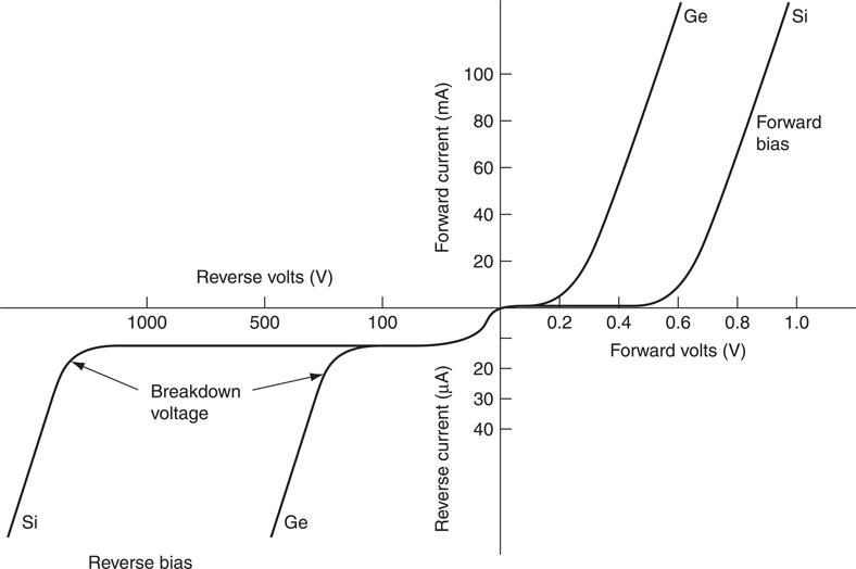
Figure 6.29 Forward and reverse bias characteristics of silicon and germanium.
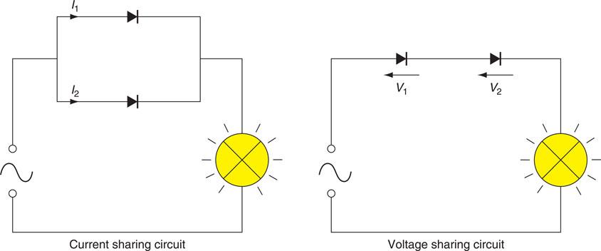
Figure 6.30 Using two diodes to reduce the current or voltage applied to a diode.
Diode testing
The p–n junction of the diode has a low resistance in one direction and a very high resistance in the reverse direction. Connecting an ohmmeter, with the red positive lead to the anode of the junction diode and the black negative lead to the cathode, would give a very low reading. Reversing the lead connections would give a high resistance reading in a ‘good’ component.
Zener diode
A Zener diode is a silicon junction diode but with a different characteristic than the semiconductor diode considered previously. It is a special diode with a predetermined reverse breakdown voltage, the mechanism for which was discovered by Carl Zener in 1934. Its symbol and general appearance are shown in Fig. 6.31. In its forward bias mode, that is, when the anode is positive and the cathode negative, the Zener diode will conduct at about 0.6 V, just like an ordinary diode, but it is in the reverse mode that the Zener diode is normally used. When connected with the anode made negative and the cathode positive, the reverse current is zero until the reverse voltage reaches a predetermined value, when the diode switches on, as shown by the characteristics given in Fig. 6.32. This is called the Zener voltage or reference voltage. Zener diodes are manufactured in a range of preferred values, for example, 2.7, 4.7, 5.1, 6.2, 6.8, 9.1, 10, 11, 12 V, etc., up to 200 V at various ratings. The diode may be damaged by overheating if the current is not limited by a series resistor, but when this is connected, the voltage across the diode remains constant. It is this property of the Zener diode which makes it useful for stabilizing power supplies and these circuits are considered in Fig. 6.32.
Definition
Zener diodes are often used in voltage stability devices in voltage regulators. A Zener will generate a small change in voltage for a given large change in current and therefore makes up for output voltage falling when load is applied.

Figure 6.31 Symbol for and appearance of Zener diodes.
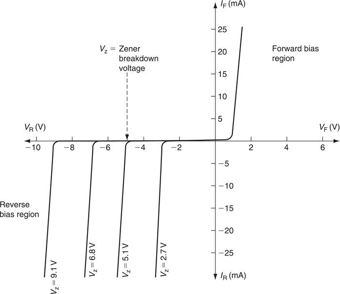
Figure 6.32 Zener diode characteristics.
If a test circuit is constructed as shown in Fig. 6.33, the Zener action can be observed. When the supply is less than the Zener voltage (5.1 V in this case) no current will flow and the output voltage will be equal to the input voltage. When the supply is equal to or greater than the Zener voltage, the diode will conduct and any excess voltage will appear across the 680 Ω resistor, resulting in a very stable voltage at the output. When connecting this and other electronic circuits you must take care to connect the polarity of the Zener diode as shown in the diagram. Note that current must flow through the diode to enable it to stabilize.
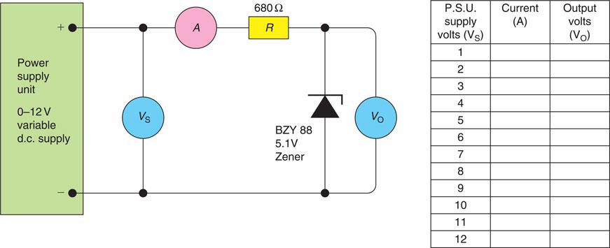
Figure 6.33 Experiment to demonstrate the operation of a Zener diode.
Light-emitting diode
The light-emitting diode (LED) is a p–n junction especially manufactured from a semi conducting material that emits light when a current of about 10 mA flows through the junction.
No light is emitted when the junction is reverse biased and if this exceeds about 5 V the LED may be damaged.
The general appearance and circuit symbol are shown in Fig. 6.34. The LED will emit light if the voltage across it is about 2 V. If a voltage greater than 2 V is to be used then a resistor must be connected in series with the LED.
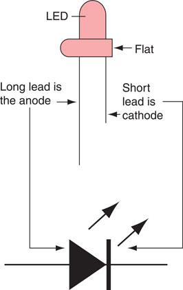
Figure 6.34 Symbol for and general appearance of an LED.
To calculate the value of the series resistor we must ask ourselves what we know about LEDs. We know that the diode requires a forward voltage of about 2 V and a current of about 10 mA must flow through the junction to give sufficient light.
The value of the series resistor R will, therefore, be given by:
The circuit is, therefore, as shown in Fig. 6.34. LEDs are available in red, yellow and green and, when used with a series resistor, may replace a filament lamp. They use less current than a filament lamp, are smaller, do not become hot and last indefinitely. A filament lamp, however, is brighter and emits white light. LEDs are often used as indicator lamps, to indicate the presence of a voltage. They do not, however, indicate the precise amount of voltage present at that point. Another application of the LED is the seven-segment display used as a numerical indicator in calculators, digital watches and measuring instruments. Seven LEDs are arranged as a figure 8 so that when various segments are illuminated, the numbers 0–9 are displayed as shown in Fig. 6.37.
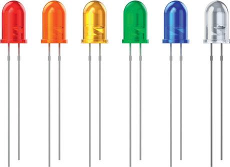
Figure 6.35 LED signal lamps.
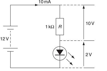
Figure 6.36 Circuit diagrams for LED example.
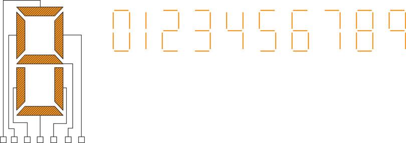
Figure 6.37 LED used in seven-segment display.
Example
Calculate the value of the series resistor required when an LED is to be used to show the presence of a 12 V supply.
Try this
LEDs
Make a list in the margin of examples where you have seen LEDs being used.
Recent scientific discoveries have also enabled this humble LED signal lamp to become the super efficient, broad spectrum general lighting service LED lamp we are familiar with today. We will look at these lamps later in this Chapter under the heading Comparison of Light Sources.
Light-dependent resistor
Almost all materials change their resistance with a change in temperature. Light energy falling on a suitable semiconductor material also causes a change in resistance. The semiconductor material of a light-dependent resistor (LDR) is encapsulated as shown in Fig. 6.38 together with the circuit symbol. The resistance of an LDR in total darkness is about 10 MΩ, in normal room lighting about 5 kΩ and in bright sunlight about 100 Ω. They can carry tens of milliamperes, an amount that is sufficient to operate a relay. The LDR uses this characteristic to switch on automatically street lighting and security alarms.
Definition
To distinguish between an LED and a LDR look at the way the arrow is pointing. LED points out (emitting), LDR points towards the device (light dependant).
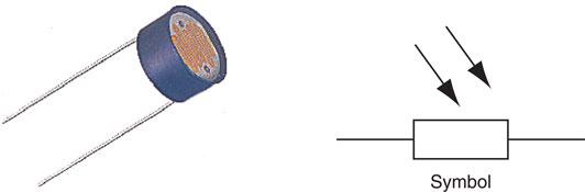
Figure 6.38 Symbol and appearance of an LDR.
Photodiode
The photodiode is a normal junction diode with a transparent window through which light can enter. The circuit symbol and general appearance are shown in Fig. 6.39 It is operated in reverse bias mode and the leakage current increases in proportion to the amount of light falling on the junction. This is due to the light energy breaking bonds in the crystal lattice of the semiconductor material to produce holes and electrons.
Photodiodes will only carry microamperes of current but can operate much more quickly than LDRs and are used as ‘fast’ counters when the light intensity is changing rapidly.
Thermistor
The thermistor is a thermal resistor, a semiconductor device whose resistance varies with temperature. Its circuit symbol and general appearance are shown in Fig. 6.40. They can be supplied in many shapes and are used for the measurement and control of temperature up to their maximum useful temperature limit of about 300°C. They are very sensitive and because the bead of semiconductor material can be made very small, they can measure temperature in the most inaccessible places with very fast response times. Thermistors are embedded in high-voltage underground transmission cables in order to monitor the temperature of the cable. Information about the temperature of a cable allows engineers to load the cables more efficiently. A particular cable can carry a larger load in winter for example, when heat from the cable is being dissipated more efficiently. A thermistor is also used to monitor the water temperature of a motor car.
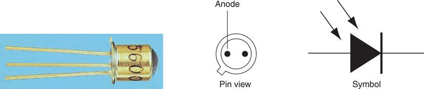
Figure 6.39 Symbol for pin connections and appearance of a photodiode.
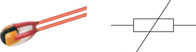
Figure 6.40 Symbol for and appearance of a thermistor.
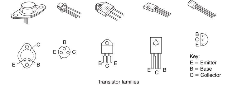
Figure 6.41 The appearance and pin connections of the transistor family.
Transistors
The transistor has become the most important building block in electronics. It is the modern, miniature, semiconductor equivalent of the thermionic valve and was invented in 1947 by Bardeen, Shockley and Brattain at the Bell Telephone Laboratories in the United States. Transistors are packaged as separate or discrete components, as shown in Fig. 6.41.
There are two basic types of transistor, the bipolar or junction transistor and the field-effect transistor (FET).
The FET has some characteristics that make it a better choice in electronic switches and amplifiers. It uses less power and has a higher resistance and frequency response. It takes up less space than a bipolar transistor and, therefore, more of them can be packed together on a given area of silicon chip.
It is, therefore, the FET that is used when many transistors are integrated on to a small area of silicon chip as in the IC that will be discussed later.
When packaged as a discrete component the FET looks much the same as the bipolar transistor. Its circuit symbol and connections are given in the Appendix. However, it is the bipolar transistor that is much more widely used in electronic circuits as a discrete component.
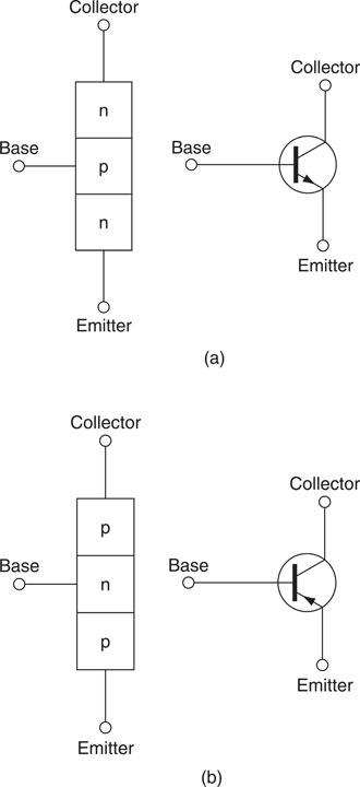
Figure 6.42 Structure of and symbol for (a) n-p-n and (b) p-n-p transistors.
The bipolar transistor
The bipolar transistor consists of three pieces of semiconductor material sandwiched together as shown in Fig. 6.42. The structure of this transistor makes it a three-terminal device having a base, collector and emitter terminal. By varying the current flowing into the base connection a much larger current flowing between collector and emitter can be controlled. Apart from the supply connections, the n-p-n and p-n-p types are essentially the same but the n-p-n type is more common.
A transistor is generally considered a current-operated device. There are two possible current paths through the transistor circuit, shown in Fig. 6.43: the base–emitter path when the switch is closed; and the collector–emitter path. Initially, the positive battery supply is connected to the n-type material of the collector, the junction is reverse biased and, therefore, no current will flow. Closing the switch will forward bias the base–emitter junction and current flowing through this junction causes current to flow across the collector–emitter junction and the signal lamp will light.
Definition
A transistor is used as both an electronic switch and as an amplifying device.
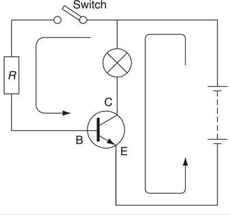
Figure 6.43 Operation of the transistor.
A small base current can cause a much larger collector current to flow. This is called the current gain of the transistor, and is typically about 100. When I say a much larger collector current, I mean a large current in electronic terms, up to about half an ampere.
We can, therefore, regard the transistor as operating in two ways: as a switch because the base current turns on and controls the collector current; and as a current amplifier because the collector current is greater than the base current.
We could also consider the transistor to be operating in a similar way to a relay. However, transistors have many advantages over electrically operated switches such as relays. They are very small, reliable, have no moving parts and, in particular, they can switch millions of times a second without arcing occurring at the contacts.
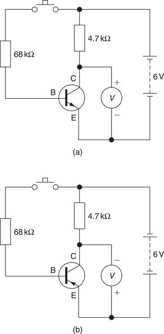
Figure 6.44 Transistor test circuits (a) n-p-n transistor test; (b) p-n-p transistor test.
Transistor testing
A transistor can be thought of as two diodes connected together and, therefore, a transistor can be tested using an ohmmeter in the same way as was described for the diode.
Assuming that the red lead of the ohmmeter is positive, the transistor can be tested in accordance with Table 6.6.
When many transistors are to be tested, a simple test circuit can be assembled as shown in Fig. 6.44.
With the circuit connected, as shown in Fig. 6.44, a ‘good’ transistor will give readings on the voltmeter of 6 V with the switch open and about 0.5 V when the switch is made. The voltmeter used for the test should have a high internal resistance, about ten times greater than the value of the resistor being tested – in this case 4.7 kΩ – and this is usually indicated on the back of a multi-range meter or in the manufacturer’s information supplied with a new meter.
Integrated circuits
ICs were first developed in the 1960s. They are densely populated miniature electronic circuits made up of hundreds and sometimes thousands of microscopically small transistors, resistors, diodes and capacitors, all connected together on a single chip of silicon no bigger than a baby’s fingernail. When assembled in a single package, as shown in Fig. 6.45, we call the device an IC.
There are two broad groups of IC: digital ICs and linear ICs. Digital ICs contain simple switching-type circuits used for logic control and calculators, and linear ICs incorporate amplifier-type circuits which can respond to audio and radio frequency signals. The most versatile linear IC is the operational amplifier, which has applications in electronics, instrumentation and control.
The IC is an electronic revolution. ICs are more reliable, cheaper and smaller than the same circuit made from discrete or separate transistors, and electronically superior. One IC behaves differently than another because of the arrangement of the transistors within the IC. Manufacturers’ data sheets describe the characteristics of the different ICs, which have a reference number stamped on the top.
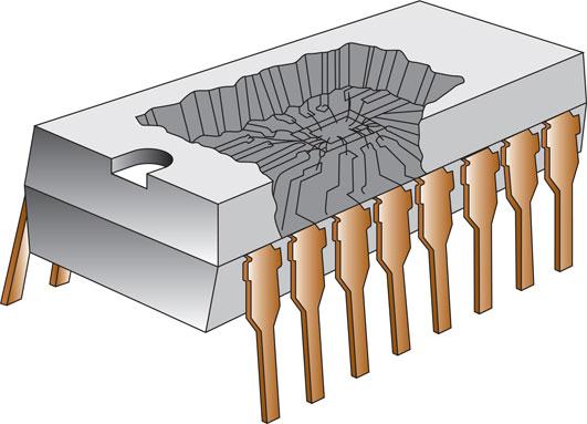
Figure 6.45 Exploded view of an IC.
When building circuits, it is necessary to be able to identify the IC pin connection by number. The number 1 pin of any IC is indicated by a dot pressed into the encapsulation; it is also the pin to the left of the cutout (Fig. 6.46). Since the packaging of ICs has two rows of pins they are called DIL (dual in line) packaged ICs and their appearance is shown in Fig. 6.47.
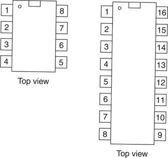
Figure 6.46 IC pin identification.
ICs are sometimes connected into DIL sockets and at other times are soldered directly into the circuit. The testing of ICs is beyond the scope of a practising electrician, and when they are suspected of being faulty an identical or equivalent replacement should be connected into the circuit, ensuring that it is inserted the correct way round, which is indicated by the position of pin number 1 as described above.
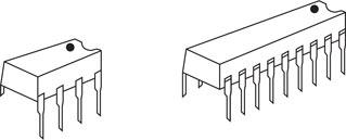
Figure 6.47 DIL packaged ICs.
The thyristor
The thyristor was previously known as a ‘silicon controlled rectifier’ since it is a rectifier that controls the power to a load. It consists of four pieces of semiconductor material sandwiched together and connected to three terminals, as shown in Fig. 6.48.
The word thyristor is derived from the Greek word thyra meaning door, because The thyristor behaves like a door. It can be open or shut, allowing or preventing current flow through the device. The door is opened – we say the thyristor is triggered – to a conducting state by applying a pulse voltage to the gate connection. Once the thyristor is in the conducting state, the gate loses all control over the devices. The only way to bring the thyristor back to a non conducting state is to reduce the voltage across the anode and cathode to zero or apply reverse voltage across the anode and cathode.
Definition
A thyristor is used in d.c. motor control since it needs a positive supply to gate it.
We can understand the operation of a thyristor by considering the circuit shown in Fig. 6.49. This circuit can also be used to test suspected faulty components. When SWB only is closed the lamp will not light, but when SWA is also closed, the lamp lights to full brilliance. The lamp will remain illuminated even when SWA is opened. This shows that the thyristor is operating correctly. Once a voltage has been applied to the gate the thyristor becomes forward conducting, like a diode, and the gate loses control.
A thyristor may also be tested using an ohmmeter as described in Table 6.7, assuming that the red lead of the ohmmeter is positive. The thyristor has no moving parts and operates without arcing. It can operate at extremely high speeds, and the currents used to operate the gate are very small. The most common application for the thyristor is to control the power supply to a load, for example, lighting dimmers and motor speed control.
The power available to an a.c. load can be controlled by allowing current to be supplied to the load during only a part of each cycle. This can be achieved by supplying a gate pulse automatically at a chosen point in each cycle, as shown by Fig. 6.50 Power is reduced by triggering the gate later in the cycle.
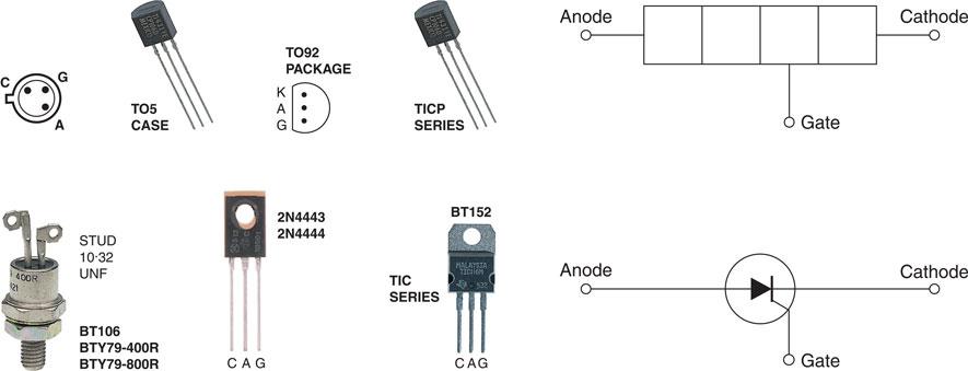
Figure 6.48 Symbol for and structure and appearance of a thyristor.
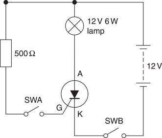
Figure 6.49 Thyristor test circuit.
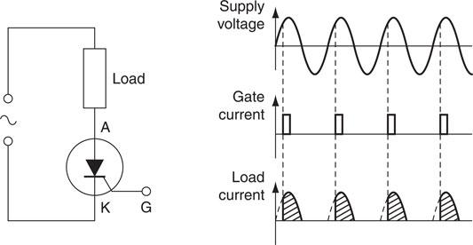
Figure 6.50 Waveforms to show the control effect of a thyristor.
The thyristor is only a half-wave device (like a diode) allowing control of only half the available power in an a.c. circuit. This is very uneconomical, and a further development of this device has been the triac, which is considered next.
Definition
A triac is used in a.c. motor control since it can be gated by either a positive or negative pulse.
The triac
The triac was developed following the practical problems experienced in connecting two thyristors in parallel to obtain full-wave control, and in providing two separate gate pulses to trigger the two devices. The triac is a single device containing a back-to-back, two-directional thyristor that is triggered on both halves of each cycle of the a.c. supply by the same gate signal. The power available to the load can, therefore, be varied between zero and full load.
Its symbol and general appearance are shown in Fig. 6.51. Power to the load is reduced by triggering the gate later in the cycle, as shown by the waveforms of Fig. 6.52.
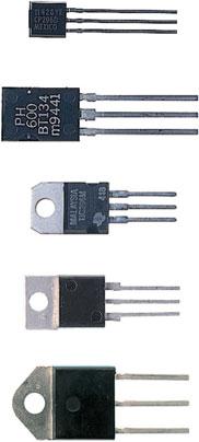
Figure 6.51 Appearance of a triac.
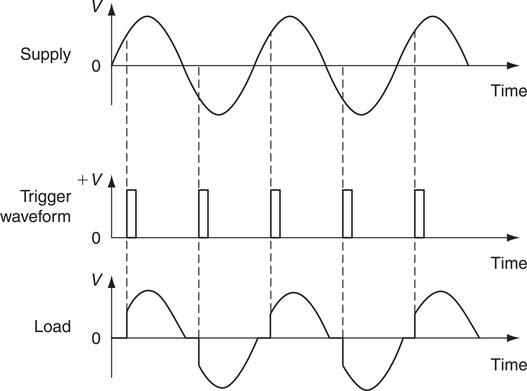
Figure 6.52 Waveforms to show the control effect of a triac.
The triac is a three-terminal device, just like the thyristor, but the terms anode and cathode have no meaning for a triac. Instead, they are called main terminal one (MT1) and main terminal two (MT2). The device is triggered by applying a small pulse to the gate (G). A gate current of 50 mA is sufficient to trigger a triac switching up to 100 A. They are used for many commercial applications where control of a.c. power is required, for example, motor speed control and lampdimming.
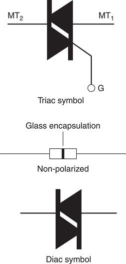
Figure 6.53 Symbol for and appearance of a diac used in triac firing circuits.
The diac
The diac is a two-terminal device containing a two-directional Zener diode. It is used mainly as a trigger device for the thyristor and triac. The symbol is shown in Fig. 6.53.
The device turns on when some predetermined voltage level is reached, say 30 V, and, therefore, it can be used to trigger the gate of a triac or thyristor each time the input waveform reaches this predetermined value. Since the device contains back-to-back Zener diodes it triggers on both the positive and negative halfcycles.
Voltage divider
Earlier in this chapter we considered the distribution of voltage across resistors connected in series. We found that the supply voltage was divided between the series resistors in proportion to the size of the resistor. If two identical resistors were connected in series across a 12 V supply, as shown in Fig. 6.54(a), both common sense and a simple calculation would confirm that 6 V would be measured across the output. In the circuit shown in Fig. 6.54(b), the 1 and 2 kΩ resistors divide the input voltage into three equal parts. One part, 4 V, will appear across the 1 kΩ resistor and two parts, 8 V, will appear across the 2 kΩ resistor. In Fig. 6.54(c) the situation is reversed and, therefore, the voltmeter will read 4 V.
The division of the voltage is proportional to the ratio of the two resistors and, therefore, we call this simple circuit a voltage divider or potential divider. The values of the resistors R1 and R2 determine the output voltage as follows:
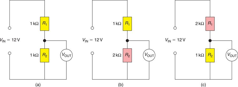
Figure 6.54 Voltage divider circuit.
Example 1
For the circuit shown in Fig. 6.55, calculate the output voltage.
Example 2
For the circuit shown in Fig. 6.56(a), calculate the output voltage.
We must first calculate the equivalent resistance of the parallel branch:
The circuit may now be considered as shown in Fig. 6.56 (b):
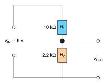
Figure 6.55 Voltage divider circuit for Example 1.
Voltage dividers are used in electronic circuits to produce a reference voltage which is suitable for operating transistors and ICs. The volume control in a radio or the brightness control of a cathode-ray oscilloscope requires a continuously variable voltage divider and this can be achieved by connecting a variable resistor or potentiometer, as shown in Fig. 6.57. With the wiper arm making a connection at the bottom of the resistor, the output would be zero. When connection is made at the centre, the voltage would be 6 V, and at the top of the resistor the voltage would be 12 V. The voltage is continuously variable between 0 and 12 V simply by moving the wiper arm of a suitable variable resistor such as those shown in Fig. 6.57.
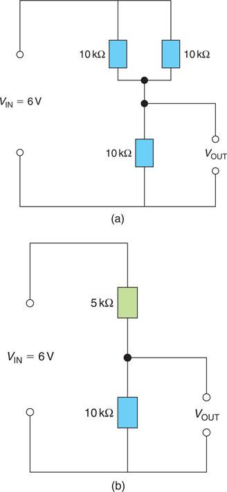
Figure 6.56 (a) Voltage divider circuit for Example 2; (b) equivalent circuit for Example 2.
When a voltmeter is connected to a voltage divider it ‘loads’ the circuit, causing the output voltage to fall below the calculated value. To avoid this, the resistance of the voltmeter should be at least ten times as great as the value of the resistor across which it is connected. For example, the voltmeter connected across the voltage divider shown in Fig. 6.54(b) must be greater than 20 k, and across 6. 54(c) greater than 10 k. This problem of loading the circuit occurs when taking voltage readings in electronic circuits and therefore a high impedance voltmeter should always be used to avoid instrument errors.
Rectification of a.c.
When a d.c. supply is required, batteries or a rectified a.c. supply can be provided. Batteries have the advantage of portability, but a battery supply is more expensive than using the a.c. mains supply suitably rectified. Rectification is the conversion of an a.c. supply into a unidirectional or d.c. supply. This is one of the many applications for a diode which will conduct in one direction only, that is when the anode is positive with respect to the cathode.
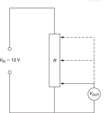
Figure 6.57 Constantly variable voltage divider circuit.
Half-wave rectification
The circuit is connected as shown in Fig. 6.58. During the first half-cycle the anode is positive with respect to the cathode and, therefore, the diode will conduct. When the supply goes negative during the second half-cycle, the anode is negative with respect to the cathode and, therefore, the diode will not allow current to flow. Only the positive half of the waveform will be available at the load and the lamp will light at reduced brightness.
Full-wave rectification
Rectification is the conversion of an a.c. supply into a unidirectional or d.c. supply.
Figure 6.59 shows an improved rectifier circuit that makes use of the whole a.c. waveform and is, therefore, known as a full-wave rectifier. When the four diodes are assembled in this diamond-shaped configuration, the circuit is also known as a bridge rectifier. During the first half-cycle diodes D1 and D3 conduct, and diodes D2 and D4 conduct during the second half-cycle. The lamp will light to full brightness.
Definition
Rectification is the conversion of an a.c. supply into a unidirectional or d.c. supply.
Full-wave and half-wave rectification can be displayed on the screen of a CRO and will appear as shown in Figs. 6.58 and 6.59.
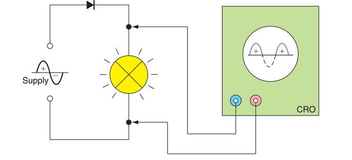
Figure 6.58 Half-wave rectification.
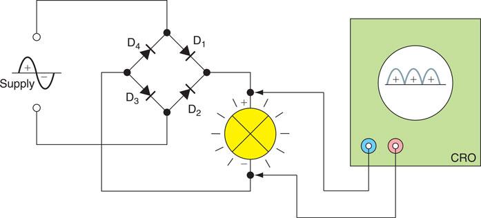
Figure 6.59 Full-wave rectification using a bridge circuit.
Smoothing
The circuits of Figs. 6.58 and 6.59 convert an alternating waveform into a waveform which never goes negative, but they cannot be called continuous d.c. because they contain a large alternating component. Such a waveform is too bumpy to be used to supply electronic equipment but may be used for battery charging. To be useful in electronic circuits the output must be smoothed. The simplest way to smooth an output is to connect a large-value capacitor across the output terminals as shown in Fig. 6.60.
When the output from the rectifier is increasing, as shown by the dotted lines of Fig. 6.61, the capacitor charges up. During the second quarter of the cycle, when the output from the rectifier is falling to zero, the capacitor discharges into the load. The output voltage falls until the output from the rectifier once again charges the capacitor. The capacitor connected to the full-wave rectifier circuit is charged up twice as often as the capacitor connected to the halfwave circuit and, therefore, the output ripple on the full-wave circuit is smaller, giving better smoothing. Increasing the current drawn from the supply increases the size of the ripple. Increasing the size of the capacitor reduces the amount of ripple.
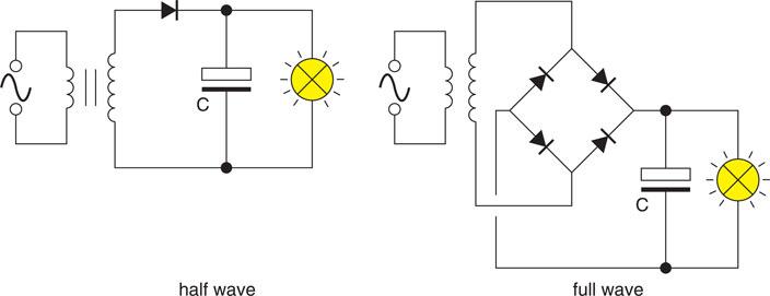
Figure 6.60 Rectified a.c. with smoothing capacitor connected.
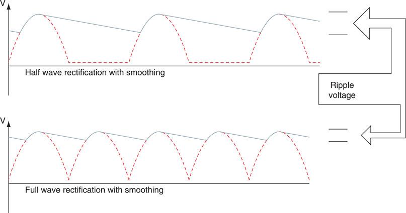
Figure 6.61 Output waveforms with smoothing, showing reduced ripple with full wave.
Try this
Battery charger
• Do you have a battery charger for your car battery?
• What type of circuit do you think is inside?
• Carefully look inside and identify the components.
Low-pass filter
The ripple voltage of the rectified and smoothed circuit shown in Fig. 6.60 can be further reduced by adding a low-pass filter, as shown in Fig. 6.61. A low-pass filter allows low frequencies to pass while blocking higher frequencies. Direct current has a frequency of zero hertz, while the ripple voltage of a full-wave rectifier has a frequency of 100 Hz. Connecting the low-pass filter will allow the d.c. to pass while blocking the ripple voltage, resulting in a smoother output voltage.
The low-pass filter shown in Fig. 6.62 does, however, increase the output resistance, which encourages the voltage to fall as the load current increases. This can be reduced if the resistor is replaced by a choke, which has a high impedance to the ripple voltage but a low resistance, which reduces the output ripple without increasing the output resistance.
Stabilized power supplies
The power supplies required for electronic circuits must be ripple-free, stabilized and have good regulation; that is, the voltage must not change in value over the whole load range. A number of stabilizing circuits are available which, when connected across the output of the circuit shown in Fig. 6.63, give a constant or stabilized voltage output. These circuits use the characteristics of the Zener diode which was described by the experiment in Fig. 6.33.
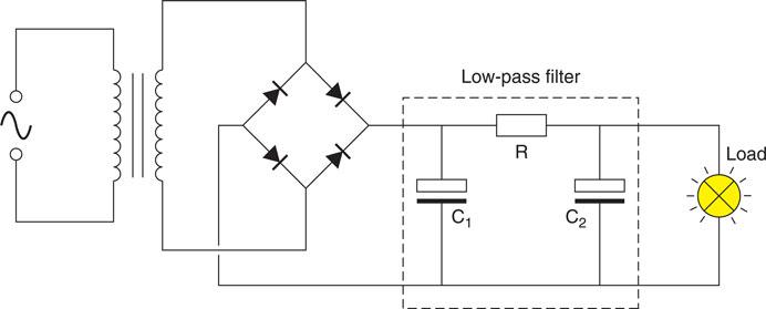
Figure 6.62 Rectified a.c. with low-pass filter connected.
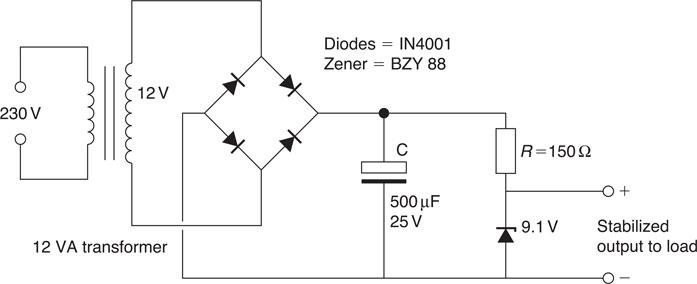
Figure 6.63 Stabilized d.c. supply.
Figure 6.63 shows an d.c. supply which has been rectified, smoothed and stabilized. You could build and test this circuit at college if your lecturers agree.
Inverter
An inverter is a device that changes direct current (d.c.) to alternating current (a.c). Mechanical versions are in existence, for instance a d.c. motor feeding an a.c. generator will convert the d.c. supplying the motor into an alternating supply as seen below.
Static inverters are much more common and use electronics that are far more reliable since they do not include any moving parts. The static inverter combines an oscillator, amplifier and a transformer in order to produce an alternating output, which is used extensively in solar photovoltaic applications in order to convert the d.c. produced by the solar cells to a mains equivalent alternating supply.
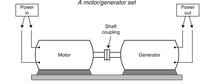
Figure 6.64 A d.c. motor feeding an a.c. generator creates a mechanical invertor: changing direct current to alternating current.
Assessment criteria 2.2
State the applications of components and devices in electrotechnical systems
Assessment criteria 2.3
Describe the function of electronic components and devices in electrotechnical systems
Intruder alarms
The installation of security alarm systems in the United Kingdom is already a multi-million-pound business and yet it is also a relatively new industry. As society becomes increasingly aware of crime prevention, it is evident that the market for security systems will expand.
Most intruders are looking for portable and easily saleable items such as DVD players, television sets, home computers, jewellery, cameras, silverware, money, cheque books or credit cards.
Security lighting
Security lighting installed on the outside of the home may be activated by external detectors. These detectors sense the presence of a person outside the protected property and additional lighting is switched on. This will deter most potential intruders while also acting as courtesy lighting for visitors (Fig. 6.65).

Figure 6.65 Security lighting reduces crime.
Passive infra-red detectors
Passive infra-red (PIR) detector units allow a householder to switch on lighting units automatically whenever the area covered is approached by a moving body whose thermal radiation differs from the background. This type of detector is ideal for driveways or dark areas around the protected property. It also saves energy because the lamps are only switched on when someone approaches the protected area. The major contribution to security lighting comes from the ‘unexpected’ high-level illumination of an area when an intruder least expects it. This surprise factor often encourages the potential intruder to ‘try next door’.
PIR detectors are designed to sense heat changes in the field of view dictated by the lens system. The field of view can be as wide as 180°, as shown by the diagram in Fig. 6.66. Many of the ‘better’ detectors use a split lens system so that a number of beams have to be broken before the detector switches on the security lighting. This capability overcomes the problem of false alarms, and a typical PIR is shown in Fig. 6.67.
Definition
Security lighting is the first line of defence in the fight against crime.
PIR detectors are often used to switch LED or tungsten halogen floodlights because, of all available luminaires, LEDs and tungsten halogen lamps offers instant high-level illumination. Light fittings must be installed out of reach of an intruder in order to prevent sabotage of the security lighting system.
Definition
PIR detector units allow a householder to switch on lighting units automatically whenever the area covered is approached by a moving body whose thermal radiation differs from the background.
Intruder alarm systems
Alarm systems are now increasingly considered to be an essential feature of home security for all types of homes and not just property in high-risk areas.
An intruder alarm system serves as a deterrent to a potential thief and often reduces home insurance premiums. In the event of a burglary they alert the occupants, neighbours and officials to a possible criminal act and generate fear and uncertainty in the mind of the intruder which encourages a more rapid departure. Intruder alarm systems can be broadly divided into three categories – those that give perimeter protection, space protection or trap protection. A system can comprise one or a mixture of all three categories.
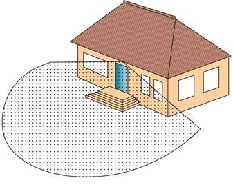
Figure 6.66 PIR detector and field of direction.
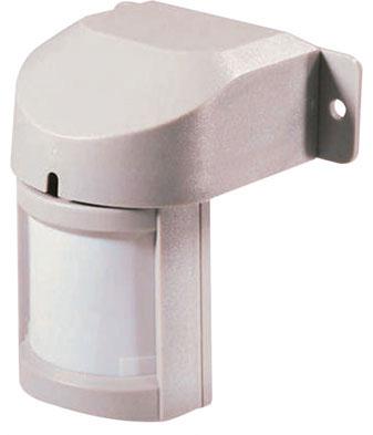
Figure 6.67 A typical PIR detector.
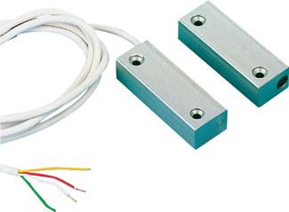
Figure 6.68 Proximity switches for perimeter protection.
A perimeter protection system places alarm sensors on all external doors and windows so that an intruder can be detected as he or she attempts to gain access to the protected property. This involves fitting proximity switches to all external doors and windows.
A movement or heat detector placed in a room will detect the presence of anyone entering or leaving that room. PIR detectors and ultrasonic detectors give space protection. Space protection does have the disadvantage of being triggered by domestic pets but it is simpler and, therefore, cheaper to install. Perimeter protection involves a much more extensive and, therefore, expensive installation, but is easier to live with.
Trap protection places alarm sensors on internal doors and pressure pad switches under carpets on through routes between, for example, the main living area and the master bedroom. If an intruder gains access to one room he cannot move from it without triggering the alarm.
Definition
An intruder alarm system serves as a deterrent to a potential thief and often reduces home insurance premiums.
A perimeter protection system places alarm sensors on all external doors and windows so that an intruder can be detected as he or she attempts to gain access to the protected property.
A movement or heat detector placed in a room will detect the presence of anyone entering or leaving that room.
Trap protection places alarm sensors on internal doors and pressure pad switches under carpets on through routes between, for example, the main living area and the master bedroom.
Proximity switches
These are designed for the discreet protection of doors and windows. They are made from moulded plastic and are about the size of a chewing-gum packet, as shown in Fig. 6.68. One moulding contains a reed switch, the other a magnet, and when they are placed close together the magnet maintains the contacts of the reed switch in either an open or closed position. Opening the door or window separates the two mouldings and the switch is activated, triggering the alarm. The same effect can be achieved using mercury switches which completes the circuit since mercury conducts electricity.
PIR detectors
These are activated by a moving body that is warmer than the surroundings. The PIR shown in Fig. 6.69 has a range of 12 m and a detection zone of 110° when mounted between 1.8 and 2 m high.

Figure 6.69 PIR intruder alarm detector.
Telephones
A component that converts one form of energy into another is known as a transducer. A telephone uses a microphone and loudspeaker to operate by converting sound into electrical signals when you speak into the phone and the complete opposite when you hear the other person. The loudspeaker uses a diaphragm that vibrates when sound waves strike against it, which in turn causes the diaphragm to create electricity by interacting with a small magnetic field.
The loudspeaker does the complete opposite: when an electrical signal is received it creates a magnetic field, which pushes and pulls a coil back and forth, which creates sound through its vibration.
A telephone also uses a tilting mechanism, which cuts the line to the exchange when the phone is rested in place.
Electrical heating control (thermostats)
Water heating or space heating systems make use of a thermostat, which is a device for maintaining a constant temperature at some predetermined value. The operation of a thermostat is often based upon the principle of differential expansion between dissimilar metals, that is, a bimetal strip, which causes a contact to make or break at a chosen temperature. Figure 6.70 shows the principle of a rod-type thermostat that is often used with water heaters. An invar rod, which has minimal expansion when heated, is housed within a copper tube and the two metals are brazed together at one end. The other end of the copper tube is secured to one end of the switch mechanism. As the copper expands and contracts under the influence of a varying temperature, the switch contacts make and break. In the case of a thermostat such as this, the electrical circuit is broken when the temperature setting is reached. Figure 6.71 shows a room thermostat which works on the same principle.
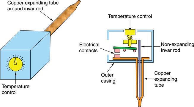
Figure 6.70 A rod-type thermostat.
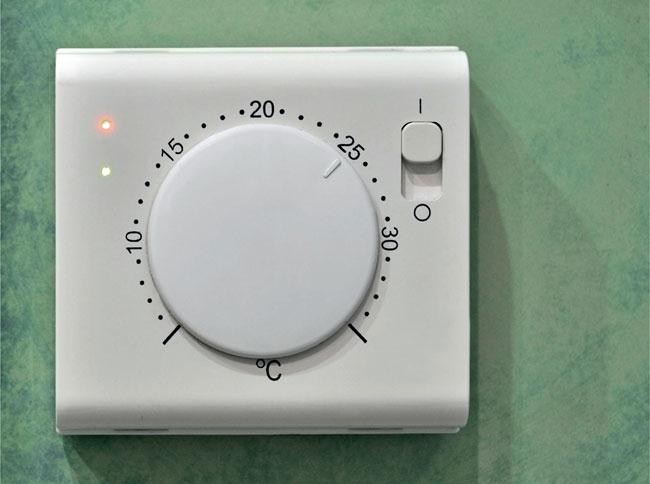
Figure 6.71 Room thermostat.
Programmers
A heating system may be fuelled by gas, oil, electricity or solar, but whatever the fuel system providing the heat energy, it is very likely that the system will be controlled by an electrical or electronic programmer, thermostats and a circulating pump for a water-based system. Fig 6.72 shows a block diagram for a typical domestic space heating and water heating system. The programmer will incorporate a time clock so that the customer or client can select the number of hours each day that the system will operate. For a working family in a domestic property this will probably be a couple of hours before the working day begins, and then five to seven hours in the evening. In a commercial situation it will probably switch on a couple of hours before the working day begins and remain on until the working day ends. In both situations the programmer unit often incorporates an override or boost facility for changing circumstances and weather conditions.
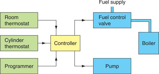
Figure 6.72 Block diagram – space heating control system (Honeywell Y plan).
During the period when the space heating or water heating is in the ‘on position’, thermostats based upon the bimetal strip principle will maintain the room and water temperature at some predetermined level. Figure 6.72 shows a wiring diagram for a domestic space and water heating system that circulates water through radiators to warm individual rooms. In this type of system, energy conservation now recommends that each radiator be additionally fitted with a TRV (thermostatic radiator valve) to control the temperature in each room.
Assessment criteria 3.1
Determine electrical quantities in alternating current circuits
In this section we will first of all consider the theoretical circuits of pure resistance, inductance and capacitance acting alone in an a.c. circuit before going on to consider the practical circuits of resistance, inductance and capacitance acting together. Let us first define some of our terms of reference.
Resistance
In d.c. circuits the resistance is defined as opposition to current flow.
From Ohm’s law:
Example 1
An electric heater, when connected to a 230 V supply, was found to take a current of 4 A. Calculate the element resistance.
Example 2
The insulation resistance measured between phase conductors on a 400 V supply was found to be 2 MH. Calculate the leakage current.
Example 3
When a 4 Ω resistor was connected across the terminals of an unknown d.c. supply, a current of 3 A flowed. Calculate the supply voltage.
Resistors in series and in parallel
In an electrical circuit resistors may be connected in series, in parallel, or in various combinations of series and parallel connections.
Series-connected resistors
In any series circuit a current I will flow through all parts of the circuit as a result of the potential difference supplied by a battery V⊤. Therefore, we say that in a series circuit the current is common throughout that circuit.
When the current flows through each resistor in the circuit, for example, R1, R2 and R3 in Fig. 6.73, there will be a voltage drop across that resistor whose value will be determined by the values of I and R, since from Ohm’s law V = I × R. The sum of the individual voltage drops, for example, V1, V2 and V3 in Fig. 6.73, will be equal to the total voltage V⊤.
 Top tip
Series resistance
The total value of resistance in a series circuit is always greater than the largest individual value.
We can summarize these statements as follows. For any series circuit, I is common throughout the circuit and
(Equation 1) |
Let us call the total circuit resistance RT From Ohm’s law we know that V = I × R and therefore
(Equation 2) |
We are looking for an expression for the total resistance in any series circuit and, if we substitute equation (2) into equation (1), we have:
Now, since I is common to all terms in the equation, we can divide both sides of the equation by I. This will cancel out I to leave us with an expression for the circuit resistance:
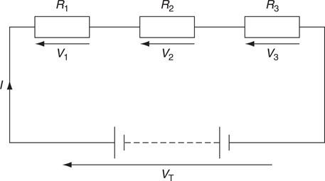
Figure 6.73 A series circuit.
Note that the derivation of this formula is given for information only. Craft students need only state the expression RT = R1 + R2 + R3 for series connections.
Parallel-connected resistors
In any parallel circuit, as shown in Fig. 6.74, the same voltage acts across all branches of the circuit. The total current will divide when it reaches a resistor junction, part of it flowing in each resistor. The sum of the individual currents, for example, I1, I2 and I3 in Fig. 6.74, will be equal to the total current IT
Key fact
Resistors
In a series circuit, total resistance RT = R1 + R2 + R3 ohms.
We can summarize these statements as follows. For any parallel circuit, V is common to all branches of the circuit and
(Equation 3) |
Let us call the total resistance RT.
Top tip
Parallel resistance
The total value of resistance in a parallel circuit is always less than the smallest individual value.
From Ohm’s law we know, that I , and therefore
(Equation 4) |
We are looking for an expression for the equivalent resistance RT in any parallel circuit and, if we substitute equations (4) into equation (3), we have:
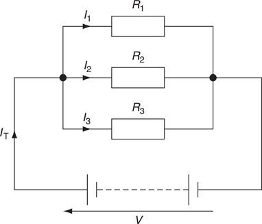
Figure 6.74 A parallel circuit.
Now, since V is common to all terms in the equation, we can divide both sides by V, leaving us with an expression for the circuit resistance:
Note that the derivation of this formula is given for information only. Craft students need only state the expression 1/RT = 1/R1 + 1/R2 + 1/R3 for parallel connections.
Key fact
Resistors
In a parallel circuit, total resistance can be found from
Example 1
Three 6Ω resistors are connected (a) in series (see Fig. 6.75), and (b) in parallel (see Fig. 6.76), across a 12 V battery. For each method of connection, find the total resistance and the values of all currents and voltages.
For any series connection
Total current
The voltage drop across R1 is
The voltage drop across R2 is
The voltage drop across R3 is
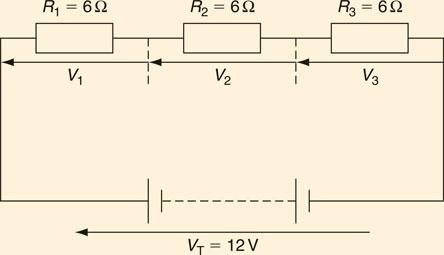
Figure 6.75 Resistors in series.
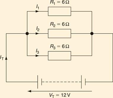
Figure 6.76 Resistors in parallel.
For any parallel connection
Total current
The current flowing through R1 is
The current flowing through R2 is
The current flowing through R3 is
Series and parallel combinations
The most complex arrangement of series and parallel resistors can be simplified into a single equivalent resistor by combining the separate rules for series and parallel resistors.
Example 2
Resolve the circuit shown in Fig. 6.77 into a single resistor and calculate the potential difference across each resistor.
By inspection, the circuit contains a parallel group consisting of R3, R4 and R5 and a series group consisting of R1 and R2 in series with the equivalent resistor for the parallel branch.
Consider the parallel group. We will label this group RP. Then
Figure 6.77 may now be represented by the more simple equivalent shown in Fig. 6.78.
Since all resistors are now in series,
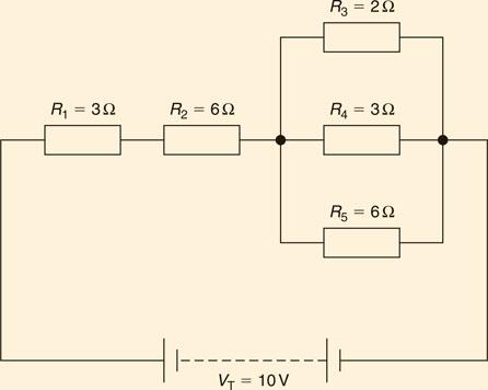
Figure 6.77 A series/parallel circuit.
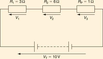
Figure 6.78 Equivalent series circuit.
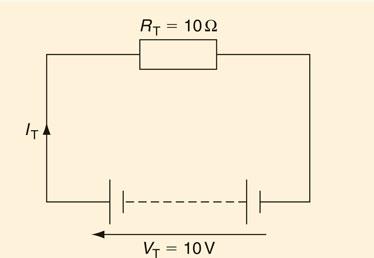
Figure 6.79 Single equivalent resistor for Fig 6.78.
Thus, the circuit may be represented by a single equivalent resistor of value 10Ω as shown in Fig. 6.79. The total current flowing in the circuit may be found by using Ohm’s law:
The potential differences across the individual resistors are
Since the same voltage acts across all branches of a parallel circuit the same p.d. of 1 V will exist across each resistor in the parallel branch R3, R4 and R5.
Example 3
Determine the total resistance and the current flowing through each resistor for the circuit shown in Fig. 6.80.
By inspection, it can be seen that R1 and R2 are connected in series while R3 is connected in parallel across R1 and R2. The circuit may be more easily understood if we redraw it as in Fig. 6.81.
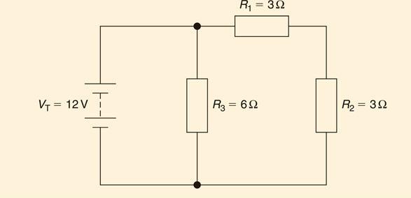
Figure 6.80 A series/parallel circuit for Example 3.
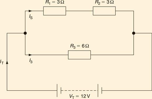
Figure 6.81 Equivalent circuit for Example 3.
For the series branch, the equivalent resistor can be found from
Figure 6.81 may now be represented by a more simple equivalent circuit, as in Fig. 6.82.
Since the resistors are now in parallel, the equivalent resistance may be found from
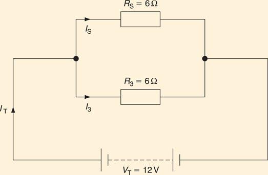
Figure 6.82 Simplified equivalent circuit for Example 2.
The total current is
Let us call the current flowing through resistor R3 I3
Let us call the current flowing through both resistors R1 and R2, as shown in Fig. 6.81, lS
Electrical power
Power and energy are related when consideration is given to the fact that energy is thought of as the amount of work that is being done or being converted and is sometimes classified as horsepower. However, when an electrical current flows in a circuit, heat is generated (energy) and the amount of heat generated depends directly on how much current is flowing (amps), which in turn depends on how much voltage or electrical pressure there is (volts).
This means that we can calculate the rate at which heat is generated through a formula for electrical Power: P = V × I, with the unit for power being represented by the watt, with one horsepower being equivalent to 746 W.
This formula is very important for an electrician since all design calculation start off by calculating how much current an installation requires. Therefore: P = V × I should be thought of as the main formula for Power for an electrician.
An effective method of remembering this formula is to use the power formula triangle
Simply cover the value required to extract the formula required.
Another two formulas for Power can be obtained by extracting values from Ohm’s law as seen below:
If V = I × R, by transposition we get
Then substitute what I represents into P = V × I
And you get
Which can be written as
Example
Calculate the current demanded by a 60 W lamp when connected to domestic mains supply of 230 V supply.
Use the main formula for power for an electrician
Transpose to find I
Resistivity
The resistance or opposition to current flow varies for different materials, each having a particular constant value. If we know the resistance of, say, 1 m of a material, then the resistance of 5 m will be five times the resistance of 1 m. The resistivity (symbol ρ – the Greek letter ‘rho’) of a material is defined as the resistance of a sample of unit length and unit cross-section. Typical values are given in Table 6.8. The resistivity of the conducting material, as well as its length and cross-sectional area are used to determine the resistance of a conductor
Table 6.8 gives the resistivity of silver as 16.4 × 10⁻⁹ Ωm, which means that a sample of silver 1 m long and 1 m in cross-section will have a resistance of 16.4 × 10⁻⁹ Ω.
It is vital that we emphasize the difference between resistance and resistivity.
• Resistance is the opposition to current flow and will include every element within the circuit including the conductor and all the internal connections linking the protective device, busbar, switch and load.
• Resistivity is concerned with the conducting material only and remains constant for a given type of material measured in Ω/m.
The resistivity formula is very important in installation work since it impacts on many aspects. Looking at the formula again
the length of the conductor is directly proportional to the overall resistance of the circuit.

Figure 6.83 Calculating the resistivity of an object.
Where
ρ = the resistivity constant for the material (Ωm)
I = the length of the material (m)
a = the cross-sectional area of the material (m2)
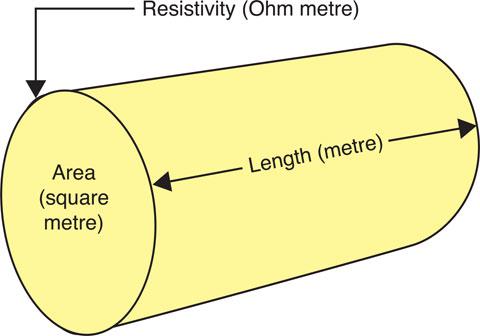
Figure 6.84 As the length of the conductor increases its resistance will increase. Resistivity, however, is based on conductor material therefore remains constant.
Directly proportional means that if the length increases so will the resistance.
Therefore, if the length of a circuit is very long, the circuit resistance will also increase. This means that more voltage will be dropped across the cable, depriving the load such as a lamp working voltage. This means that a lamp can appear dim, or motor circuits could run slower than expected. How do we compensate for this?
Again, looking at the formula the cross-sectional area of the conductor is indirectly proportional to the overall resistance of the circuit.
Definition
Resistivity is concerned with conductor material.
Indirectly proportional means that if the area increases the resistance will decrease accordingly. Therefore when we encounter volt drop problems we counter this by increasing the cross-sectional area of a cable, in other words: select a bigger size. To summarize the relationship between resistivity and resistance:
Increasing the length increases the resistance.
Increasing the area decreases the resistance.
Decreasing the length decreases the resistance.
Decreasing the area increases the resistance.
Doubling the length doubles the resistance.
Doubling the area halves the resistance.
Calculating resistivity
The general rule that you need to remember when working out any problem with regard to resistivity is to make sure that the units that you use are consistent, i.e. all the units have to be in metres or millimetres. However, whilst cable length and resistivity tend to be represented in metres and Ω/m respectively, cable size is normally represented in mm2.
A handy rule to remember when converting millimetres to metres is to attach the magic number x 10-6. We obtain this number from the fact that 1 metre contains 1000 mm. But cable size is actually cross-sectional area which is measured in m2 therefore the difference between millimetres and metres can be shown by 6 decimal places or the magic number 10−6. 1.5 mm2 would therefore become 1.5 × 10⁻⁶ m2.
Material |
Resistivity (Ωm) |
|---|---|
Silver |
16.4 × 10⁻⁹ |
Copper |
17.5 × 10⁻⁹ |
Aluminium |
28.5 × 10⁻⁹ |
Brass |
75.0 × 10⁻⁹ |
Iron |
100.0 × 10⁻⁹ |
Example 1
Calculate the resistance of 100 m of copper cable of 1.5 mm2 cross-sectional area (csa) if the resistivity of copper is taken as 17.5 × 10⁻⁹ Ωm.
Example 2
Calculate the resistance of 100 m of aluminium cable of 1.5 mm2 crosssectional area if the resistivity of aluminium is taken as 28.5 × 10⁻⁹ Ωm.
Key fact
Resistance: If the length is doubled, resistance will be doubled. If the csa is doubled, the resistance will be halved.
The above examples show that the resistance of an aluminium cable is some 60% greater than a copper conductor of the same length and cross-section. Therefore, if an aluminium cable is to replace a copper cable, the conductor size must be increased to carry the rated current as given by the tables in Appendix 4 of the IET Regulations and Appendix 6 of the On-Site Guide.
The other factor which affects the resistance of a material is the temperature, and we will consider this later.
Try this
Resistance
• Take two 100 m lengths of single cable (2 coils)
• Measure the resistance of 100 m of cable (1 coil)
• Value ______________________________Ω
• Join the two lengths together (200 m) and again measure the resistance
• Value ______________________________Ω
• Does this experiment prove resistance is proportional to length?
• If the resistance is doubled, it is proved (QED)! (QED, quod erat demonstradum, is the Latin for ‘which was to be demonstrated’.)
Assessment criteria 3.2
Explain the relation between resistance, inductance, impedance and capacitance
a.c. circuits
In an a.c. circuit, resistance is only part of the opposition to current flow. The inductance and capacitance of an a.c. circuit also cause an opposition to current flow, which we call reactance.
Definition
Inductive reactance (XL) is the opposition to an a.c. current in an inductive circuit. It causes the current in the circuit to lag behind the applied voltage.
Inductive reactance (XL) is the opposition to an a.c. current in an inductive circuit. It causes the current in the circuit to lag behind the applied voltage, as shown in Fig. 6.85. It is given by the formula:
Where
π = 3.142 (a constant)
f = the frequency of the supply
L = the inductance of the circuit, or by:
Definition
In any circuit, resistance is defined as opposition to current flow.
Capacitive reactance (XC) is the opposition to an a.c. current in a capacitive circuit. It causes the current in the circuit to lead ahead of the voltage, as shown in Fig. 6.85. It is given by the formula:
Definition
Capacitive reactance (Xc) is the opposition to an a.c. current in a capacitive circuit, It causes the current in the circuit to lead ahead of the voltage.
where π and f are defined as before and C is the capacitance of the circuit. It can also be expressed as:
Definition
Inductance is the ability a coil has to store energy in a magnetic field.
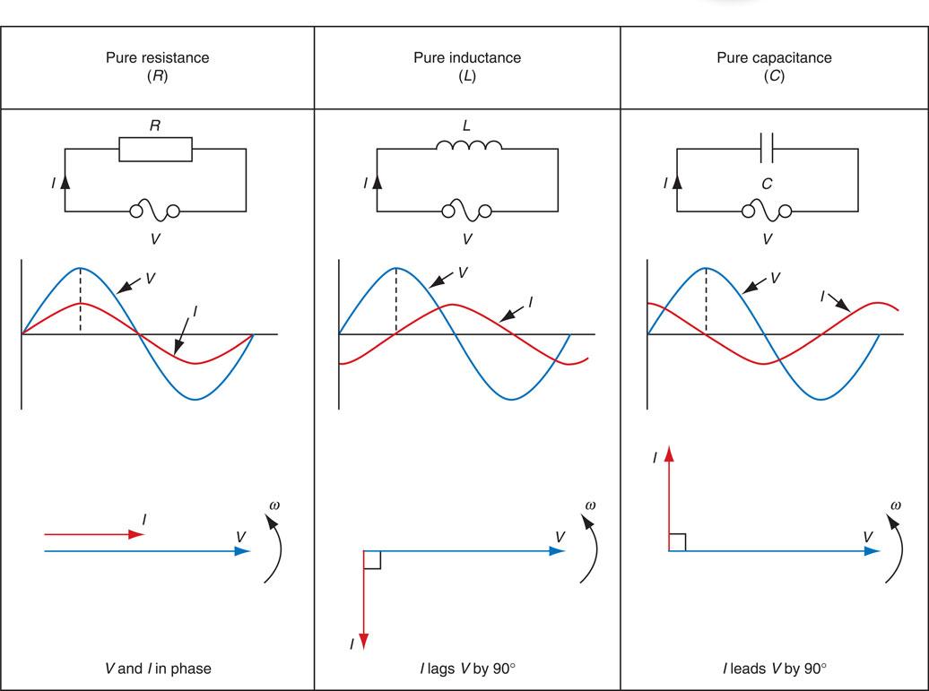
Figure 6.85 Voltage and current relationships in resistive, capacitive and inductive circuits.
Example
Calculate the reactance of a 150 μF capacitor and a 0.05 H inductor if they were separately connected to the 50 Hz mains supply.
For capacitive reactance:
where f = 50 Hz and C = 150 μF = 150 × 10−6 F
For inductive reactance:
where f = 50 Hz and L = 0.05 H
Impedance
The total opposition to current flow in an a.c. circuit is called impedance and given the symbol Z. Thus impedance is the combined opposition to current flow of the resistance, inductive reactance and capacitive reactance of the circuit and can be calculated from the formula:
Definition
The total opposition to current flow in an a.c. circuit is called impedance and given the symbol Z.
Example 1
Calculate the impedance when a 5Ω resistor is connected in series with a 12Ω inductive reactance.
Definition
Self inductance is when a coil produces a back e.m.f. which actually opposes the current that produced it.
Example 2
Calculate the impedance when a 48Ω resistor is connected in series with a 55Ω capacitive reactance.
Definition
Mutual inductance is when a rate of change in current in one coil produces an e.m.f in another coil.
Impedance can also be represented when we have a combination of resistance, inductive reactance as well as capacitive reactance. The formula for impedance becomes:
Resistance, inductance and capacitance in an a.c. circuit
When a resistor only is connected to an a.c. circuit the current and voltage waveforms remain together, starting and finishing at the same time. We say that the waveforms are in phase.
When a pure inductor is connected to an a.c. circuit the current lags behind the voltage waveform by an angle of 90°. We say that the current lags the voltage by 90°. When a pure capacitor is connected to an a.c. circuit the current leads the voltage by an angle of 90°. These various effects can be observed on an oscilloscope, but the circuit diagram, waveform diagram and phasor diagram for each circuit are shown in Fig. 6.85.
Phasor diagrams
Phasor diagrams and a.c. circuits are an inseparable combination. Phasor diagrams allow us to produce a model or picture of the circuit under consideration, which helps us to understand the circuit. A phasor is a straight line, having definite length and direction, which represents to scale the magnitude and direction of a quantity such as a current, voltage or impedance. To find the combined effect of two quantities we combine their phasors by adding the beginning of the second phasor to the end of the first. The combined effect of the two quantities is shown by the resultant phasor, which is measured from the original zero position to the end of the last phasor.
Definition
A phasor is a straight line, having definite length and direction, which represents to scale the magnitude and direction of a quantity such as a current, voltage or impedance.
Example
Find by phasor addition the combined effect of currents A and B acting in a circuit. Current A has a value of 4 A, and current B a value of 3 A, leading A by 90°. We usually assume phasors to rotate anticlockwise and so the complete diagram will be as shown in Fig. 6.86. Choose a scale of, for example, 1 A=1 cm and draw the phasors to scale; that is, A = 4 cm and B = 3 cm, leading A by 90°.
The magnitude of the resultant phasor can be measured from the phasor diagram and is found to be 5 A acting at a phase angle ϕ of about 37° leading A. We therefore say that the combined effect of currents A and B is a current of 5 A at an angle of 37° leading A.
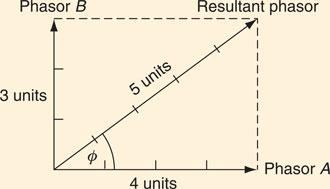
Figure 6.86 The phasor addition of currents A and B.
Phase angle ϕ
In an a.c. circuit containing resistance only, such as a heating circuit, the voltage and current are in phase, which means that they reach their peak and zero values together, as shown in Fig. 6.87a.
In an a.c. circuit containing inductance, such as a motor or discharge lighting circuit, the current often reaches its maximum value after the voltage, which means that the current and voltage are out of phase with each other, as shown in Fig. 66.87(a), the phase difference, measured in degrees between the current and voltage, is called the phase angle of the circuit, and is denoted by the symbol ϕ, the lower-case Greek letter phi. When circuits contain two or more separate elements, such as RL, RC or RLC, the phase angle between the total voltage and total current will be neither 0° nor 90° but will be determined by the relative values of resistance and reactance in the circuit. This is shown by figures 6.87(b) and 6.87(c) respectively whereby the phase angle between applied voltage and current is represented by the angle ϕ.
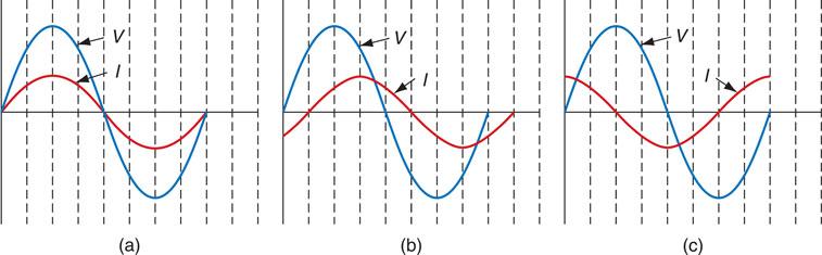
Figure 6.87 Phase relationship of a.c. waveform: (a) V and I in phase, phase angle ϕ = 0° and power factor = cos ϕ = 1; (b) V and I displaced by 45°, ϕ = 45° and p.f. = 0.707; and (c) V and I displaced by 90°, ϕ = 90° and p.f. = 0.
Alternating current series circuits
In a circuit containing a resistor and inductor connected in series as shown in Fig. 6.88, the current I will flow through the resistor and the inductor causing the voltage VR to be dropped across the resistor and VL to be dropped across the inductor. The sum of these voltages will be equal to the total voltage VT but because this is an a.c. circuit the voltages must be added by phasor addition. The result is shown in Fig. 6.88, where VR is drawn to scale and in phase with the current and VL is drawn to scale and leading the current by 90°. The phasor addition of these two voltages gives us the magnitude and direction of VT, which leads the current by some angle ϕ.
In a circuit containing a resistor and capacitor connected in series as shown in Fig. 6.89, the current I will flow through the resistor and capacitor causing voltage drops VR and VC. The voltage VR will be in phase with the current and VC will lag the current by 90°. The phasor addition of these voltages is equal to the total voltage VT which, as can be seen in Fig. 6.89, is lagging the current by an angle ϕ.
Definition
An inductor causes the circuit current to lag the circuit voltage.
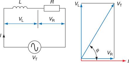
Figure 6.88 A series RL circuit and phasor diagram.

Figure 6.89 A series RC circuit and phasor diagram.
The impedance triangle
We have now established the general shape of the phasor diagram for a series a.c. circuit. Figures 6.88 and 6.89 show the voltage phasors, but we know that VR = IR, VL = IXL, VC = IXC and VT = IZ, and therefore the phasor diagrams (a) and (b) of Fig. 6.90 must be equal. From Figure 6.90(b), by the theorem of Pythagoras, we have:
If we now divide throughout by I2 we have:
The phasor diagram can be simplified to the impedance triangle given in Fig. 6.90(c).
Definition
By transposing the impedance triangle we can define power factor
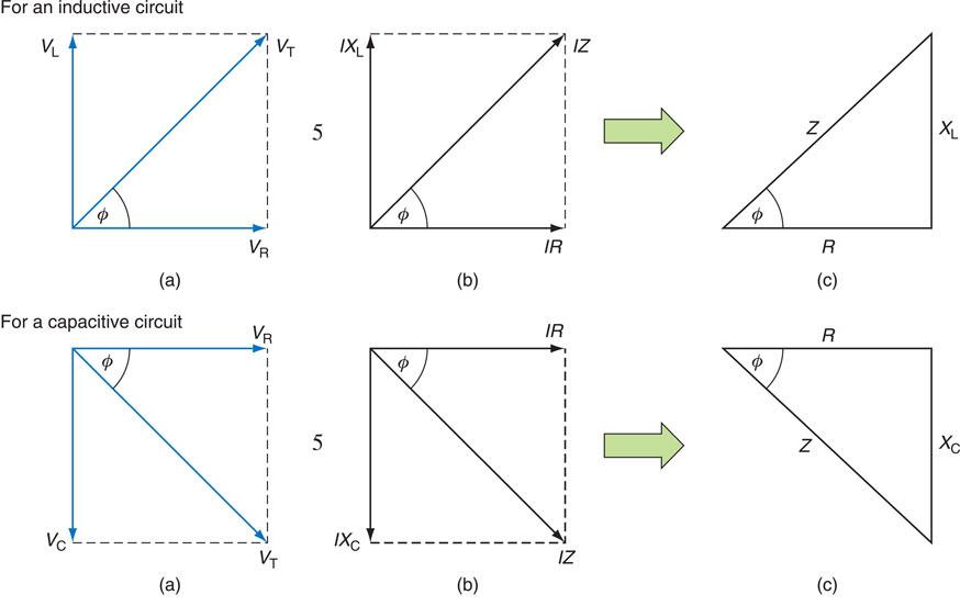
Figure 6.90 Phasor diagram and impedance triangle.
Example 1
A coil of 0.15 H is connected in series with a 50Ω resistor across a 100 V 50 Hz supply. Calculate (a) the reactance of the coil, (b) the impedance of the circuit, and (c) the current.
For (a)
For (b)
For (c)
Example 2
A 60 μF capacitor is connected in series with a 100Ω resistor across a 230 V 50 Hz supply. Calculate (a) the reactance of the capacitor, (b) the impedance of the circuit and (c) the current.
For (a)
For (b)
For (c)
Assessment criteria 3.3
Determine power quantities in alternating current circuits
Assessment criteria 3.4
Explain the relation between power quantities in alternating current circuits
Assessment criteria 3.5
Calculate power factor
Power and power factor
Power factor (p.f.) is defined as the cosine of the phase angle between the current and voltage:
Definition
Power factor (p.f.) is defined as the cosine of the phase angle between the current and voltage.
If the current lags the voltage as shown in Fig. 6.88, we say that the p.f. is lagging, and if the current leads the voltage as shown in Fig. 6.89, the p.f. is said to be leading. From the trigonometry of the impedance triangle shown in Fig. 6.90, p.f. is also equal to:
The electrical power in a circuit is the product of the instantaneous values of the voltage and current. Figure 6.91 shows the voltage and current waveform for a pure inductor and pure capacitor. The power waveform is obtained from the product of V and I at every instant in the cycle. It can be seen that the power waveform reverses every quarter cycle, indicating that energy is alternately being fed into and taken out of the inductor and capacitor. When considered over one complete cycle, the positive and negative portions are equal, showing that the average power consumed by a pure inductor or capacitor is zero. This shows that inductors and capacitors store energy during one part of the voltage cycle and feed it back into the supply later in the cycle. Inductors store energy as a magnetic field and capacitors as an electric field.
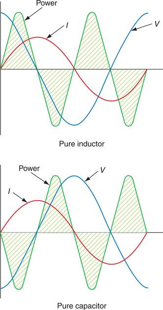
Figure 6.91 Waveform for the a.c. power in purely inductive and purely capacitive circuits.
In an electric circuit more power is taken from the supply than is fed back into it, since some power is dissipated by the resistance of the circuit, and therefore:
In any d.c. circuit the power consumed is given by the product of the voltage and current, because in a d.c. circuit voltage and current are in phase. In an a.c. circuit the power consumed is given by the product of the current and that part of the voltage which is in phase with the current. The in-phase component of the voltage is given by V cos φ, and so power can also be given by the equation:
The power factor of most industrial loads is lagging because the machines and discharge lighting used in industry are mostly inductive. This causes an additional magnetizing current to be drawn from the supply, which does not produce power, but does need to be supplied, making supply cables larger.
Key fact
If power factor is not corrected then electrical machines draw more current, cables have to be made bigger, the system is very inefficient and in some cases companies can be fined.
Example 1
A coil has a resistance of 30Ω and a reactance of 40Ω when connected to a 250V supply. Calculate (a) the impedance, (b) the current, (c) the p.f., and (d) the power.
For (a)
For (b)
For (c)
For (d)
Example 2
A capacitor of reactance 12Ω is connected in series with a 9Ω resistor across a 150 V supply. Calculate (a) the impedance of the circuit, (b) the current, (c) the p.f., and (d) the power.
For (a)
For (b)
For (c)
For (d)
Power factor can also be represented through the power triangle as seen in Fig. 6.92.
Example 3
A 230 V supply feeds three 1.84 kW loads with power factors of 1, 0.8 and 0.4. Calculate the current at each power factor.
The current is given by:
where P = 1.84 kW = 1840 W and V = 230 V. If the p.f. is 1, then:
For a p.f. of 0.8:
For a p.f. of 0.4:
It can be seen from these calculations that a 1.84 kW load supplied at a power factor of 0.4 would require a 20 A cable, while the same load at unity power factor could be supplied with an 8 A cable. There may also be the problem of higher voltage drops in the supply cables. As a result, the supply companies encourage installation engineers to improve their power factor to a value close to 1 and sometimes charge penalties if the power factor falls below 0.8.
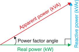
Figure 6.92 From the power triangle we can extract the formula for power factor (pF) = Apparent power/Real power.
As explained previously, due to the inherent nature of inductive loads and their reactive component, a back e.m.f. is created that then acts against the circuit current and causes it to lag the voltage. This produces reactive power and is represented by KVAr, but because the current and voltage are not acting together, the power produced is known as wattles. In other words, a form of useless power. When the power factor operates at unity (1) then these issues are not evident but this is simply not possible since all loads tend to include an inductive component and can be seen in such items as: motors, generators, fluorescent lights and relays etc.
In comparison, true power is also known by many aliases such as real power and active power but the one I prefer is working power measured in Watts since it’s what actually powers our equipment and unlike reactive power is very useful.
However, what we actually pay for is KVA apparent power, in other words the combination of working and reactive power, which is shown through the pint of beer analogy since although you pay for a whole pint, the froth is useless.
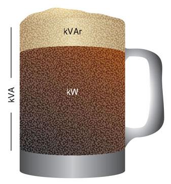
Figure 6.93 The beer analogy – you pay for the whole pint (kVA), the froth is useless power (kVAr) and the real power is the useful or worthwhile element (kW).
Given that power factor is always represented by cosine, this means we can also write this as an equation.
An example involving the power triangle can be shown below:
If the circuit working power (real power is) 9 kW and the apparent power is 10 kW, calculate the power factor.
Definition
By transposing the power triangle we can deti ne power factor
Assessment criteria 3.6
Explain the term power factor correction
Assessment criteria 3.7
Specify the methods of power factor correction
Power factor correction
Most installations have a low or bad power factor because of the inductive nature of the load. A capacitor has the opposite effect of an inductor, and so it seems reasonable to add a capacitor to a load that is known to have a lower or bad power factor, for example, a motor. Referring back to the power triangle, power factor correction is also endeavouring to make apparent power equal to working power by eliminating or reducing the effects of reactive power.
Figure 6.94(a) shows an industrial load with a low power factor. If a capacitor is connected in parallel with the load, the capacitor current IC leads the applied voltage by 90°. When this capacitor current is added to the load current as shown in Fig.6.94(b) the resultant load current has a much improved power factor. However, using a slightly bigger capacitor, the load current can be pushed up until it is ‘in phase’ with the voltage as can be seen in Fig. 6.94(c).
Capacitors may be connected across the main bus-bars of industrial loads in order to provide power factor improvement; this is called bulk correction. Alternatively, smaller capacitors may also be connected across an individual piece of equipment, as is the case for fluorescent light fittings.
A further method of correcting power factor is to use synchronous motors, a type of motor used in precision and timing applications. The field and excitation can be adjusted so that the motor effectively behaves likes a capacitor and causes the current to lead and therefore counters the effect of other inductive loads. A disadvantage of using synchronous motors to correct power factor issues is the relatively high cost involved compared with other methods.
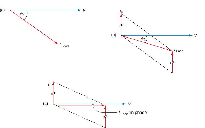
Figure 6.94 Power factor improvement using capacitors.
Assessment criteria 3.8
Determine the neutral current in a three-phase four wire system
Star and delta connections
The three-phase windings of an a.c. generator may be star connected or delta connected, as shown in Fig. 6.95. The important relationship between phase and line currents and voltages is also shown. The square root of is simply a constant for three-phase circuits, and has a value of 1.732. The delta connection is used for electrical power transmission because only three conductors are required. Delta connection is also used to connect the windings of most three-phase motors because the phase windings are perfectly balanced and, therefore, do not require a neutral connection.
Making a star connection at the local substation has the advantage that two voltages become available – a line voltage of 400 V between any two phases, and a phase voltage of 230 V between line and neutral which is connected to the star point.
In any star-connected system currents flow along the lines (IL), through the load and return by the neutral conductor connected to the star point. In a balanced three-phase system all currents have the same value and, when they are added up by phasor addition, we find the resultant current is zero. Therefore, no current flows in the neutral and the star point is at zero volts. The star point of the distribution transformer is earthed because earth is also at zero potential. A star connected system is also called a three-phase four-wire system and allows us to also derive single-phase loads from a three-phase system as shown in Fig 6.95.