2
Atomic-scale Study of Fullerene Molecules on Semiconductor Surfaces
R.Z. Bakhtizin1 and A.I. Oreshkin2
1Bashkir State University, Department of Physical Electronics and Nanophysics, 32 Zaki Validi Street, Ufa 450076, Russia
2Moscow State University, Faculty of Physics, Department of Quantum Electronics, GSP-1, 1-2 Leninskiye Gory, Moscow 119991, Russia
2.1 Introduction
Organic materials are becoming popular and important components of the modern electronic devices. The study of carbon materials has attracted growing interest in recent years, due to the discovery of new allotropic forms of carbon (fullerenes, carbon nanotubes, and graphene). These discoveries were rewarded with prestigious scientific prizes and opened up new possibilities for considerably changing our lives. Self-organizing nanostructures based on fullerene molecules and their fluorinated derivatives compatible with Si-based semiconductor systems are currently of great interest for expanding microelectronic technologies to nanoscale range and for applications in optoelectronic devices [1]. Fluorine atoms directly bound to the fullerene cage give fluorofullerene molecules their impressive electron-acceptor properties, making it easier for trap and confinement of electrons. So, fluorinated fullerenes are promising materials for organic electronics due to their pronounced electron-acceptor properties: even in a free state, they can easily capture thermal electrons forming long-lived (up to seconds) negative ions [2]. Such fluorofullerene molecules are some of the best n-type organic semiconductors available to make bulk heterojunction photovoltaic cells and field-effect transistors. That is why fluorofullerenes can be used in creating effective solar batteries. For example, the high reactivity of C60F36 allows to apply this fluorinated fullerene as a dopant to create a p-type of conductivity in pentacene that is used to create organic light-emitting Schottky diodes. Moreover, fluorinated fullerenes are characterized by high oxidative capacity that is important for their employment as cathode material in lithium ion batteries.
In addition, to create single-molecule technologies, it is very important to study the interaction between these molecules and substrate and observe the changes in the electronic structure of a compound. Below the interactions between fluorinated derivatives of fullerene C60 and silicon surfaces at the atomic level are described using scanning tunneling microscopy (STM) and scanning tunneling spectroscopy (STS) under ultrahigh vacuum conditions.
2.2 STM Study of C60 Adsorption on Solid Surface
The development of technology of producing fullerenes in macroscopic amounts appeared first in papers on the interaction of these molecules with surface of solid (including the use of STM [3,4]). It has been shown that C60 molecules are disordered on Si(111) surfaces, demonstrating their strong interaction with the substrate due to the high concentrations of dangling bonds at the surface; after deposition, the probability of their diffusion is low. Similar behavior has been observed on Si(100) surface, where the rotation of molecules also ceased; in some cases, this allowed observation of their internal structure. On metal surfaces (Cu and Ag), C60 molecules move over flat terraces and stabilize at the edges of steps, which is not surprising because the steps on metal surfaces are more active. Unlike the step edges, a large number of reconstructions emerge on the edges of terraces on semiconductor surfaces, lowering the surface free energy by reducing the number of dangling bonds. As the degree of coverage increases, the molecules begin to group into two-dimensional islands. Recently, we observed a similar behavior of C60 molecules on Si(111) surfaces covered with thick semimetal Bi layers [5] (group III metals can completely passivate Si(111) surfaces by saturating the dangling bonds of Si). Fullerene molecules on such surfaces interact with substrate through weak van der Waals forces; they diffuse freely and form ordered islands even at submonolayer coatings. Besides STS has revealed there is no appreciable charge transfer between molecules and surfaces: the position of the LUMO peak did not depend on a C60 layer's thickness [5].
2.3 C60F18 on Si(111)
The first STM experiments with fluorofullerenes have been done in Ref. [6]. At that time C60 molecules were fluorinated under flowing fluorine conditions that resulted in a mixture of molecules: C60F46 (mainly) and small amounts of C60F42, C60F44, and C60F48. Such molecules readily react with the silicon surface giving a fluorine atom to form a Si-F compound even at room temperature. Since then, the methods of synthesis of fullerene derivatives have been greatly improved. Recently, the fluorinated fullerene C60F18 has been obtained in high abundance and even a crystalline phase has been developed [7–9]. In contrast to C60Fn (n = 42–48) molecules, the tortoise-shaped polar C60F18 molecule (electric dipole moment >9 Debye) is very asymmetrical, as it is shown in Figure 2.1.
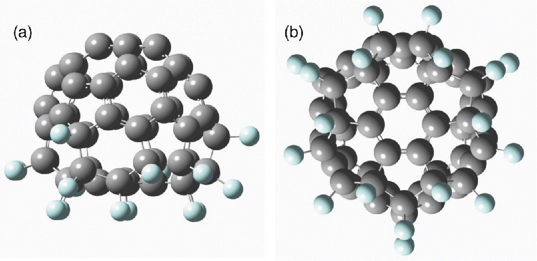
Figure 2.1 (a) A tortoise-shaped flattened C60F18 fluorofullerene (side view) in which F atoms adsorb on one half of a C60 molecule and (b) a view along the threefold symmetry direction of the molecule. Blue (gray) balls represent F (C) atoms. Alternate parallel (F–C–C–F) and perpendicular (F–C–C–F) arrangements can be noticed on a ring around the central hexagon [9].
The structure of the molecule has been determined to have all the 18 fluorine atoms bound to only one hemisphere of C60. The addition of F atoms makes four nearest neighbors around each such carbon atom and the local bonding character changes from predominantly sp2 to sp3 type, and the C–C bonds elongate in the range of 1.5–1.6 Å.1 There is a six-membered ring of sp2 bonded carbon atoms (alternate bond lengths 1.372 and 1.376 Å) that is isolated from the residual molecular system by a “belt” of sp3-hybridized C atoms, each having an F atom as shown in Figure 2.1b. That is why F atoms flatten this molecule and the Ih symmetry of C60 reduces to a threefold rotational symmetry (C3v) in C60F18. Following the notations in the Schlegel diagram in Ref. [7], the calculated C–C bond distances lie in the range of 1.37–1.68 Å and agree well with the experimental values. The shortest bonds are associated with sp2 bonded carbon atoms, while the longest bonds with C–C bonds in pentagons having F atoms. The calculated highest occupied–lowest unoccupied (HOMO–LUMO) molecular orbital gap of C60H18 is 2.41 eV as compared to 1.65 eV for pure C60, while the mean calculated binding energy of an F atom on C60 is 3.6 eV, indicating that C60F18 is a very stable molecule.
Here we present the results of STM imaging of individual C60F18 molecules deposited on a Si(111)-7 × 7 surface combined with ab initio pseudopotential calculations based on density functional theory to obtain the atomic arrangement and electronic structure of these supported molecules [10].
To prepare pure C60F18, a new method of fluorination of C60 in solid-state reactions with transition metal fluorides (MnF3 or K2PtF6) was employed. This technology was developed by Prof. L. Sidorov and his group at MSU [7–9]. Fluorination was conducted under Knudsen cell conditions with mass spectrometric identification of gaseous products. As a rule, the mass spectrum contained two main peaks that were identified as corresponding to C60 and C60F18, respectively, and a few additional peaks that were attributed to the fragments of C60F18 molecules that arose from the loss of some fluorine atoms under electron ionization. The deposition of C60F18 molecules has been performed from Knudsen cell on a Si(111)-7 × 7 surface kept at room temperature. The deposition rate was in the range of 0.05–0.1 ml min−1. All experiments were carried out at room temperature using ultrahigh-vacuum scanning tunneling microscope (base pressure 2 × 10⁻¹¹ Torr) equipped with standard surface preparation facilities. A phosphorus-doped Si(111) wafer with resistivity of 1.6 Ω cm (the nominal doping concentration was ∼8 × 1017 cm−3) was cut into pieces of 20 × 7 × 0.5 mm3 and than ultrasonically washed in acetone and distilled water. Samples were mounted on a tantalum sample holder using “Ni-free” tools and the surface was cleaned by outgassing overnight at 650 °C and then flashing at 1250 °C for 5 s followed by slow cooling. In situ STM measurements were carried by using electrochemically etched W tips as well as commercial Pt-Ir tips.
The details of the spatially varying charge density as observed in our high-resolution STM images (Figure 2.2) were analyzed from ab initio pseudopotential calculations using plane wave projector-augmented wave method [11]. The exchange correlation energy has been calculated within generalized gradient approximation (GGA) [12]. Isolated C60F18 molecule, clean Si(111)-7 × 7 surface, and adsorption of C60F18 on it have been studied using a supercell with sufficient vacuum space between the molecules/surfaces so that the interaction between the periodic images is minimal. We followed the dimer-adatom-stacking-fault (DAS) model [13] for the 7 × 7 reconstruction of Si(111) surface and studied adsorption using a slab having six layers out of which bottom three layers were kept frozen. The dangling bonds on the bottom side of the slab were saturated with H atoms. All the ions in the remaining layers as well as the molecule in the supercell were allowed to relax without any symmetry constraints using conjugate gradient method. The Brillouin zone of the supercell was sampled by the gamma point in the case of isolated molecules, while 2 × 2 × 2 Monkhorst–Pack k-points were used for the surface calculations [14]. Ionic relaxation was continued until the force on each ion became less than 0.01 eV/Å and the energy difference between the successive ionic steps was lower than 10−5 eV.
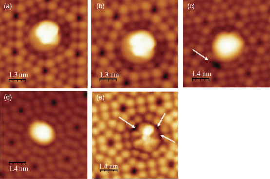
Figure 2.2 STM images of a single C60F18 molecule adsorbed on a corner site of Si(111)-7 × 7 surface at constant tunneling current It = 20 pA. (a), (b), and (c) correspond to filled states images at a bias voltage Us = −1.8 V, −2.0 V, and −2.0 V, respectively. The STM image in (c) was obtained some time later than the STM image in (b). (d) and (e) show empty states images at Us = +1.8 V. The STM image in (e) was obtained some time later than the STM image in (d). White arrows in (c) and (e) indicate some F atoms leaving C60F18 molecule and getting adsorbed on the surface during measurements.
The lowering of the symmetry of C60 by the attachment of F atoms to one part of the cage will influence the properties of the remaining part as well as the ordering and packing of the fullerene molecules on Si(111)-7 × 7 surface depending upon the interactions of the fullerene cage or attached atoms with the surface. From our STM data, we conclude that the initial nucleation of the deposited C60F18 molecules occurs on three different positions of the Si(111)-7 × 7 surface unit cell, namely, the unfaulted half, the faulted half, and the corner hole. In this work, we focus on the study of C60F18 adsorption on a corner hole of the Si(111)-7 × 7 surface unit cell. The corner hole adsorption site was used for further analysis since its symmetry allows us to analyze in detail the interaction between C60F18 molecule and Si adatoms on the Si(111)-7 × 7 surface. Our results show that at room temperature generally the adsorbed fluorofullerene molecules initially did not react with Si(111)-7 × 7 surface and also there was no movement of C60F18 on the Si(111)-7 × 7 surface except for the occasional tendency to move from a corner hole to a faulted half position during STM measurements.
Figure 2.2 shows STM images of the filled states of a C60F18 molecule located above a corner hole of Si(111)-7 × 7 surface at −1.8 V (Figure 2.2a) and −2.0 V sample bias (Figure 2.2b and c). There is a bright spot in place of the corner hole of the Si(111)-7 × 7 surface. The images are similar, but the bright spot in Figure 2.2a is distinctly smaller in comparison with that in Figure 2.2b. Figure 2.2c shows the image at −2.0 V sample bias taken moments after the STM image presented in Figure 2.2b. One can observe the appearance of black spot (shown by an arrow) in this STM image.
The STM images of the unoccupied states taken at +1.8 V bias are shown in Figure 2.2d and e. The STM image presented in Figure 2.2e was obtained some time later than the STM image presented in Figure 2.2d. The central part of the image changes drastically with the applied bias. There is a small spot of high intensity and five spots of much lower intensity. One can also notice the appearance of some black spots in the image depicted in Figure 2.2e. The black regions in Figure 2.2c and e increase with time and are indicative (see below) of some F atoms leaving C60F18 molecule and getting adsorbed on the surface (as illustrated by white arrows in Figure 2.2c and e).
To understand the adsorption properties of fluorofullerenes, we considered three different orientations of a C60F18 molecule on Si(111)-7 × 7 surface: (i) a “bottom orientation” where most of the F atoms directly interact with the surface (molecule shown in Figure 2.2a landing on the hole of Si(111)-7 × 7 surface unit cell in a nearly threefold symmetric arrangement), (ii) a “top orientation,” in which F atoms are in the top position so that only C atoms can interact with the surface, and (iii) a “side orientation,” in which the fullerene is in between the top and the bottom orientations and a few F atoms interact with the surface. In all cases, the positions of the atoms in the molecule were fully relaxed, as discussed earlier. The adsorption energy of the molecule, Ead is calculated from

where E(C60F18), E(Si), and E(C60F18/Si) are the total energies of a free C60F18 molecule, Si(111)-7 × 7 surface, and the combined system, respectively. Among the three different orientations of a C60F18 molecule considered on Si(111)-7 × 7 surface, the adsorption energy for the bottom orientation is very high (6.65 eV) compared to 1.75 eV for the top and 1.79 eV for the side orientations (Figure 2.3). Accordingly, it is expected that C60F18 molecule would instantaneously align to the bottom orientation, with the fluorine atoms pointing toward the Si adatoms.

Figure 2.3 (i–iii) Three possible orientations of C60F18 molecule on Si(111)-7 × 7 surface.
In order to further elucidate the experimentally obtained STM images, we have calculated the total and the partial densities of states (DOS) for the bottom orientation case and these are shown in Figure 2.4. It is seen that the Fermi energy (EF) lies in a band of states of Si(111)-7 × 7 surface, while the occupied and the unoccupied states of the C60F18 molecule are energetically well separated with a gap of about 2.1 eV. The 2p states of F atoms are fully occupied and lie more deeply as compared to the highest occupied 2p states of C atoms. Therefore, STM images from the filled states in our experiments arise mainly from C-2p and Si-3p orbitals. From our calculations, no C60F18 state lies between EF and EF-2.0 eV (see the bottom two curves), but some states exist between ∼2.1 and 3.9 eV below EF, predominantly on C atoms (some differences in the calculated and observed values of energies are possible due to the bandgap problem in GGA). Accordingly, the STM image of the filled states of the adsorbed C60F18 molecule at −2.0 V is largely due to C-2p states.
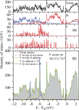
Figure 2.4 (a) The total and the partial electronic densities of states (DOS) of bottom-oriented C60F18 molecule adsorbed on Si(111)-7 × 7 surface. The zero of energy corresponds to EF. The partial density of states on F atoms lies mostly about 4 eV below EF. Black, blue, and red lines correspond to total DOS, and s and p partial DOS of the respective atoms. (b) The total and the partial electronic DOS for an F atom adsorbed on an adatom site and at a rest atom site on Si(111)-7 × 7 surface. The partial DOS of F atom lies mostly about 5.0 eV below the Fermi energy and therefore no current is expected in the STM images of Si surface around such sites at the used bias. The change in the total DOS of the Si(111)-7 × 7 surface after adsorption of F in the two cases is quite small.
To explain the STM images from the empty states (Figure 2.2d and e), we find that in the calculated DOS (Figure 2.4a), the main contribution is again coming from Si and C atoms. There are several peaks in the partial DOS of C atoms in the energy range of EF and 2.0 eV above it. In the experimental STM image obtained at +1.8 V, the C60F18 molecule looks as a bright spot surrounded by Si adatoms. We relate the drastic changes in the STM image at +1.8 V bias in Figure 2.2e with the detachment of some fluorine atoms from C60F18 molecule. In view of the appearance of some black spots, it is concluded that some F atoms have detached from the fluorofullerene molecule in the period of the experiment and moved on to the surface region where black spots are seen. This leads to modification in the electronic structure of the fluorofullerene and the possibility of direct Si–C interaction that changes the STM image. This conclusion is supported from our calculations on the binding of an F atom on Si(111)-7 × 7 surface. It is found that the binding energy of an F atom on Si(111)-7 × 7 surface is 7.55 and 7.44 eV on adatom and rest atom sites, respectively, with the Si–F bond lengths of 1.63 and 1.65 Å. The difference in the values is small and the F atom could be on either site. Also as shown in Figure 2.4b, the changes induced in the DOS of the Si(111)-7 × 7 surface due to adsorption of F atom are small and the features due to F atom appear well below the EF. This suggests again that no image would be seen from the regions of Si(111) surface having F atoms with the bias used in our experiments. The binding energy of F on Si surface is nearly twice the mean value obtained for F atoms on C60. Therefore, there is a very strong energy gain if an F atom moves to the surface, though some compensation can be expected from rebonding within the fluorofullerene and possible chemical bond formation between Si and C atoms. Therefore, our results support the migration of F atoms from C60F18 molecule to Si(111) surface. This can be expected to lead to asymmetry seen in the experimental image.
We have also modeled the STM images using calculations of the charge isocontours from filled states by accumulating charge density from states in the energy range of EF-2.25 eV to EF and the cuts in planes parallel to the surface and passing above the Si adatoms and above the fluorofullerene molecule (Figure 2.5a–b). In the plane above the Si adatoms (Figure 2.5a), one can see high density around the adatoms, while the cut above the fluorofullerene (Figure 2.5b) shows electronic charge density distribution that has similar features as seen in STM images (Figure 2.2a and b). The C60F18 molecule situated above a corner hole of Si(111)-7 × 7 surface appears as a bright spot of a slightly asymmetric shape. The intensity of spot is also not uniform and it is spatially distributed in the range of molecule image. Our calculated results for +0.8 V bias (a lower value of voltage is taken as the bandgap is underestimated in GGA) show that the charge density is mainly located at the top of C60F18 molecule in a pentagon and hexagon rings. Similar behavior has been observed in our experimental results (Figure 2.2d) where STM image of C60F18 molecule looks as bright spot of symmetrical shape. The results of the DOS calculation further confirm that F atoms in C60F18 molecule are oriented toward the surface. If F atoms would be on the top position, then we shall see no current in STM images at this bias.
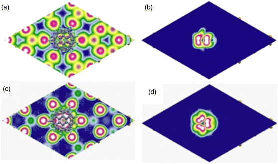
Figure 2.5 Isocontours (blue corresponds to 0.0 and white to 0.02 e/Å3) of charge density distribution for a single C60F18 molecule on a corner hole of Si(111)-7 × 7 surface in a plane (a) 1.86 Å and (b) 9.32 Å above the center of Si adatom corresponding to filled states with Us = −2.25 V, while (c) and (d) correspond to empty states with Us = +0.8 V at heights as in (a) and (b).
To understand the interaction mechanism of the fluorofullerene molecule with the surface, we have calculated the difference Δρ of the charge densities for the free molecule and free Si(111) surface and the adsorbed systems for the case of the bottom oriented C60F18 molecule on the surface. It should be noted that in experiment we always observe the dependence ρ(C60F18/Si) but not Δρ = ρ(C60F18/Si) − ρ(C60F18) − ρ(Si); therefore, we cannot expect a strict conformity of the theory with experiments. Figure 2.6a and b show that the main effect of adsorption is the polarization of the Si(111)-7 × 7 surface, whereas the charge density distribution in the molecule is not affected much. The dipole-like formation of the charge density distribution on the surface is observed around six Si adatoms that are near the corner hole where the molecule is adsorbed. This is induced by the large dipole moment in C60F18. The electronic charge density distribution of the induced dipole moments close to the adatom sites is, however, not uniform and there are alternately low and high densities due to the atomic arrangement in C60F18 molecule, where F–C–C–F units are located (nearly) parallel and perpendicular to the surface alternatively as shown in Figure 2.6a and b. In the perpendicular configuration, the F atoms are nearer to the surface adatoms and it leads to stronger polarization. There is also higher density of charge on pairs of C atoms sharing a hexagon and a pentagon in the same direction in C60F18 fluorofullerene that supports the feature that appears to have three lobes in the STM image. Intensity distribution in the simulated STM image shows that charge is attracted toward Si atoms that are close to F atoms. The interesting point here is that excess of charge is not on F atoms. The reason for this behavior is that C60F18 molecule has a large HOMO–LUMO gap and as such it is not able to get more charge from Si surface. There is a small depletion of charge on F atoms (green color) and some excess on C atoms (magenta), which is seen clearly in Figure 2.6. This means that F atoms can interact a little bit with nearest-neighbor Si atoms and share some charge with them. Since only a few F atoms lie close to Si adatoms, the excess charge near Si atoms appears prominent. This leads to the formation of induced dipole on the surface. In the layer below the surface, there is depletion as one should expect.

Figure 2.6 Modeling results: charge densities difference (a) and dipole-like charge distribution on the surface due to polarization induced by the dipole moment of the molecule (b) show top and side views of the difference in the electronic charge densities of the adsorbed system (C60F18 + surface) and the sum of the densities of free C60F18 molecule and the Si surface, Δρ = ρ(C60F18/Si) − ρ(C60F18) − ρ(Si). Magenta and green isosurfaces (∼1.3 × 10⁻⁵ electrons/Å3) represent the excess and the depletion of charge, respectively. The excess of charge is more significant around those Si surface adatoms that are close to F atoms perpendicular to the surface orientation.
Further, our results show that there is no significant charge transfer between the C60F18 molecule and the surface and the large binding energy (∼6.65 eV) of the molecule with the surface is due to induced polarization. The smallest Si–F bond distance is approximately 3 Å and it confirms that there is no significant chemical bonding between the surface and the molecule.
Interestingly, we also found that the molecule tilts slightly and shifts toward one side of the corner hole to optimize the interaction and it also agrees with the image obtained from the experiment that is slightly asymmetrical.
2.4 C60F18 on Si(100)-2 × 1
We observed the similar behavior for an individual C60F18 molecule on Si(100)-2 × 1 surface [15]. The deposition of C60F18 has been performed from Knudsen cell on a Si(100)-2 × 1 surface kept at room temperature. The deposition rate was in the range of 0.05–0.1 ml min−1. All experiments were carried out at room temperature. Phosphorus-doped Si(100) wafers with resistivity of 8 ÷ 15 Ω cm were cut into pieces of 20 × 7 × 0.5 mm3 and then ultrasonically washed in acetone and distilled water. Samples were mounted on a tantalum sample holder using “Ni-free” tools and the surface was cleaned by outgassing overnight at 650 °C and then flashing at 1250 °C for 20 s followed by slow cooling at rates of ≤2 °C/s from 950 °C to room temperature. In situ STM experiments were carried out at room temperature by using commercial Pt-Ir tips. Figure 2.7 shows the initial stage of the adsorption of C60F18 molecules on a Si(100)-2 × 1 surface. From STM data, we conclude that the initial nucleation of deposited C60F18 molecules can occur on either sites (steps or terraces) of Si(100)-2 × 1 surface. Moreover, two additional features are clearly distinguished from the STM images: we observed a zigzag buckling of dimers that form c(4 × 2) reconstruction in the vicinity of the adsorbed C60F18 molecules. Similar pattern was observed in Ref. [16] when the influence of defects on a clean Si surface was studied and also in the case [17] where the authors studied C60 adsorption on Si(100)-2 × 1 surface. We also noted that almost all C60F18 molecules deposited at room temperature are located in the troughs in between the dimer rows and randomly distributed across the surface. For C60 adsorption on Si(100)-2 × 1 surface, this feature has been originally highlighted in Ref. [18] and confirmed in Ref. [17]. Four-dimer or two-dimer sites in the trough have been considered. To estimate which adsorption site is preferable in our case, we used high resolution STM image, which shows clear dimer structures of Si(100)-2 × 1 surface and adsorbed C60F18 molecules that appear as billiard-ball-like protrusions on the surface. We drew several lines along the (0 1 1) direction (parallel to the Si–Si dimer axis) in the range of adsorbed individual C60F18 molecule. From this scheme, it is clearly seen that the center of molecule is located exactly in the trough between two dimer rows. The lateral size of the C60F18 molecules observed by STM is 20 Å. It is easy to calculate because the distance between the adjacent dimers in a row is well known to be 3.84 Å. The experimental value of the lateral size of the molecule is larger than the real one due to the fact that the STM is convolution of the electronic density of states (DOS) of the sample and the tip.

Figure 2.7 The initial stage of C60F18 molecules' adsorption on the Si(100)-2 × 1 surface. Filled states' STM image. U = −2.0 V; I = 20 pA. C60F18 molecules.
The corresponding optimized atomic structure with buckled dimers is shown in Figure 2.8. In this case, the Si(100) surface was modeled with a six-layer slab with hydrogen on one side of the slab. The bottom layers were kept frozen and the upper layers were fully optimized. The buckled dimers can be seen in Figure 2.8. The C60F18 molecule was placed on a dimer row to begin with and the optimized structure shows some tilting in the trough between the dimer rows. The molecule covers approximately the area of a 3 × 3 unit cell of dimers. The adsorption energy of C60F18 molecule has the maximum value of ∼12.1 eV for the orientation with F atoms pointing toward the surface. The adsorption energy is higher than the value on Si(111)-7 × 7 surface (6.65 eV) due to the larger number of dangling bonds on Si(100) surface. Therefore, as on Si(111)-7 × 7 surface, we would expect the C60F18 molecule to adsorb on Si(100) surface with F atoms pointing toward the surface. The spectrum of the normalized tunneling conductivity measured above the surface sites with monolayer coverage is presented in Figure 2.9. Six distinct peaks are clearly distinguished at bias range from −4.0 V to +4.0 V. There are three maxima at negative sample voltage (−3.6 V, −1.6 V, and −1.6 V) and three maxima at positive sample voltage (0.5 V, 1.8 V, and 2.8 V). In order to understand this, we have shown in Figure 2.10a both the calculated DOS of Si(100)-2 × 1 surface and the spectrum of C60F18 molecule, while in Figure 2.10b, the total and partial DOS of C60F18 molecule adsorbed on Si(100)-2 × 1 surface are shown. From the results of DOS in Figure 2.10b, the maximum at −0.6 V in the tunneling conductivity is responsible for the π-bonded state of Si(100)-2 × 1 electronic structure [19] (see a peak below the EF). The presence of π*-antibonding state (see a peak above the EF) is masked by the LUMO state of adsorbed C60F18 molecule (see a peak around the same energy for the adsorbed C60F18 molecule). The relative intensity of these peaks is in general consistent between measurements and always has a smaller value than the intensity of other observed maxima. We ascribe two other peaks at negative sample bias at −1.6 V and at −3.6 V to the C60F18 states (see peaks at around −2.1 and −3.7 eV in the partial DOS of C60F18 in Figure 2.10b). The small differences are likely to be due to the approximation of the exchange–correlation functional. Our values of peak positions agree well with the experimental data of Ref. [20], where the values of 1.8 and 3.2 eV for HOMO and HOMO-1 levels, respectively, have been obtained by means of photoelectron spectroscopy. The small discrepancies in the observed values are due to the substrate influence. The authors in Ref. [20] used a thin SiO2 interlayer to prevent both the chemical interaction of fullerenes with Si substrate and the contribution of substrate signal into the top of valence band spectra. The peaks at 1.8 and at 2.8 eV are apparently responsible for the unoccupied levels of C60F18, as one can see states around these energies in the partial DOS of C60F18 in Figure 2.10b. From these results, we can also conclude that the HOMO–LUMO gap of the adsorbed molecule is reduced compared to the value for an isolated molecule (compare Figure 2.10a and b). From the observed STS spectra and the calculated results, we can decide that the electronic structure of the fluorofullerenes is very sensitive to substrate influence.
Figure 2.8 The ball and stick model of C60F18 molecule adsorbed on a Si(100)-2 × 1 surface. The surface modeled by a slab of six layers with H terminating the dangling bonds on one side.
Figure 2.9 Normalized tunneling conductivity measured above 1 ml of C60F18 molecule on Si(100)-2 × 1 surface.
Figure 2.10 The calculated density of states for (a) a clean Si(100)-2 × 1 surface (shaded region) and the spectrum of isolated C60F18 molecule; (b) total DOS of adsorbed C60F18 molecule on Si(100)-2 × 1 surface and the partial DOS of C60F18 molecule.
2.5 C60F36 on Si(111)-7 × 7
Using the same technology of synthesis (solid-state reactions with transition metal fluorides [7–9]), the thermodynamically stable fluorinated fullerene molecules C60F36 with magic numbers of fluorine atoms have been obtained, while the structure of these molecules was reliably established [21]. This high-temperature fluorination of C60 yielded three main isomers of C60F36: C3 and C1 isomers in 2 : 1 ratio and 2% of T-symmetric structures (Figure 2.11) [22,23]. We could directly observe for the first time with STM the presence of isomers with different symmetry (T, C3, and C1) [24].
Figure 2.11 The structure of C60F18 isomers with T (a), C3 (b), and C1 (c) symmetry; the benzenoid rings and double bonds are highlighted [23].
Due to their thermal stability, fluorofullerenes C60F36 can be transferred into the gas phase without decomposition so the deposition of these molecules was performed from Knudsen cell on a clean Si(111)-7 × 7 surface kept at room temperature. The deposition rate was 0.05–0.1 ml min−1. STM and STS under ultrahigh-vacuum conditions (4 × 10⁻¹¹ Torr) have also been used to study the initial stages of adsorption of these molecules on Si(111)-7 × 7 surface. Spatially resolved images of an individual C60F36 fluorofullerene molecules on Si(111)-7 × 7 surface have been obtained using these techniques. We used z(V) spectroscopy and current imaging tunneling spectroscopy (CITS) technique [25,26], whereby the tunneling current–voltage (I–V) curves were recorded at each pixel of a scanning area, while the tunneling gap was fixed by momentarily turning off the feedback loop. To map the surface local density of states (LDOS), we numerically calculated the normalized tunneling conductance, (dI/dV)/(I/V), which is independent of the transmission factor [27]. The basic principle of z(V) spectroscopy is similar to CITS mode. But in this regime, the dependence of tunneling gap from bias voltage is fixed with engaged feedback at each pixel of a scanned area. Unlike conventional I(V) spectroscopy, where the strong increase in tunneling current I with bias voltage V exists at higher voltages, z(V) spectroscopy allows to hold the tunneling current fixed at any value by the feedback loop.
Figure 2.12 shows the initial stage of C60F36 molecule adsorption on a Si(111)-7 × 7 surface. We concluded from STM data that the initial nucleation of C60F36 molecules can occur on either sites (steps or terraces) of Si(111)-7 × 7 surface. Moreover, high-resolution STM images of C60F36 molecules adsorbed on Si(111)-7 × 7 surface revealed the presence of molecules with different symmetry (Figure 2.13). The presence of isomers with different symmetry (T, C3, and C1) has been revealed for the first time during this STM investigation. Measurements were performed in constant current mode. Bias voltage and tunneling current were kept constant during measurements. The possibility to obtain STM image in Figure 2.13c was higher than the possibility to reveal two others. Our previous analysis of the low-symmetry fullerene adsorption processes on Si(111)-7 × 7 surface proved that such molecules interact with substrate being oriented relative to the surface in the exactly same manner independent of adsorption site due to strong surface polarization (Figures 2.12 and 2.13). This statement allowed us to eliminate the explanation that three different STM observed in our experiments represent only one low-symmetry C1-C60F36 fullerene in different projections. Therefore, one can conjecture that according to [22] the STM image in Figure 2.13c demonstrates C3-C60F36 fluorofullerene. The probability to find STM image depicted in Figure 2.13a was the least. This fact allows us to conclude that indeed three different types of symmetry for C60F36 molecule exist and can be found in STM experiments. The observed symmetry of molecules can be explained by the presence of C60F36 isomers of different symmetry (T, C3, and C1) [22], formed on Si(111)-7 × 7 surface during deposition. All tunneling spectra obtained in our experiments were measured above the most often observed on Si(111)-7 × 7 surface C3-C60F36 fluorofulerene molecules. The normalized tunneling conductivity spectrum measured above the surface site containing individual molecule of C60F36 is presented in Figure 2.14. Seven distinct peaks are clearly resolved at the whole bias range from −2.5 to +2.5 V. There are three maxima at negative sample voltage (−1.6 V, −0.8 V, and −0.2 V) and four maxima at positive sample voltage (+0.55 V, +0.9 V, +1.4 V, and +2.1 V). The maxima in (dI/dV)/(I/V) spectrum denoted as A, B, C, and D are typical for Si(111)-7 × 7 structure and are responsible for adatoms and rest atoms [28]. The remaining three peaks are responsible for HOMO and LUMO orbitals of adsorbed C60F36 molecule. It is possible to conclude from our measurements that the HOMO–LUMO gap of adsorbed C60F36 molecule is about 3.0 eV. Obtained data corresponded well to measurements obtained with employment of z(V) mode with engaged feedback measurements (Figure 2.15). The application of z(V) mode slightly restricts the measurement accuracy, but in our case its employment is reasonable due to negligible influence for C60F36 molecule. The configuration of C60F36 molecule remains unchanged. Three central peaks (−0.85 V, −0.23 V, and +0.4 V) in Figure 2.15 are responsible for features of Si(111)-7 × 7 substrate, while three remaining maxima correspond to HOMO, LUMO, and LUMO+1 orbitals of adsorbed C60F36 molecule on Si(111)-7 × 7 surface. The maximum denoted as C in Figure 2.14 is not resolved in z(V) mode. Both spectroscopic methods reveal correct energy peak positions and consequently allow to estimate the HOMO–LUMO orbitals of adsorbed molecule. The comparative peaks' amplitudes differ for both methods due to methodology of measurements described above and do not include any important information.
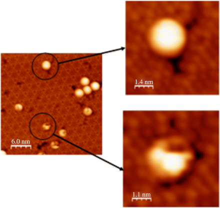
Figure 2.12 The initial stage of C60F36 molecules' adsorption on a Si(111)-7 × 7 surface.
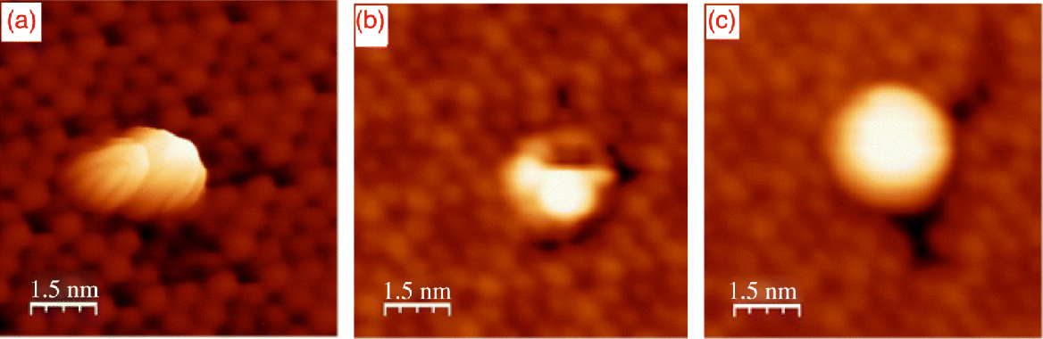
Figure 2.13 Three different high-resolution STM images of C60F36 molecules adsorbed on a Si(111)-7 × 7 surface; Us = −2.0 V, It = 40 pA.
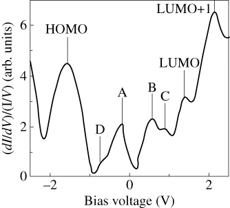
Figure 2.14 The normalized tunneling conductivity spectrum measured above C60F36 molecule.
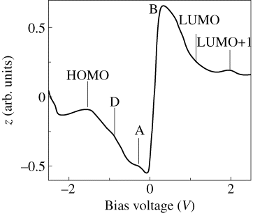
Figure 2.15 The spectrum of z(V) measured above C60F36 molecule.
2.6 Conclusions
In conclusion, we have performed STM measurements and ab initio calculations on the adsorption of individual polar C60F18 molecules on Si(111)-7 × 7 surface [29]. It is found that polar fluorinated carbon fullerene has large binding energy on a corner hole site of Si(111)-7 × 7 surface due to induced polarization on the Si surface. Calculations also suggest that C60F18 molecule binds on the Si surface with F atoms interacting with the surface. No image should be seen at the used bias voltage in STM experiments if F atoms are situated on the top position. The high binding energy of F atoms on adatom and rest atom sites of Si surface and the appearance of black spots in images lead us to conclude that during the time of the experiment, F atoms tended to migrate to the surface. Such a possibility has been known in studies of other higher fluorinated fullerenes, but in C60F18, this tendency is weaker due to the higher stability of C60F18 molecule.
We have also conducted STM measurements and ab initio calculations of individual polar C60F18 molecules adsorbed on Si(100)-2 × 1 surface. It has been shown that C60F18 molecules are located in the troughs in between dimer rows. The calculations of the adsorption energy show that the orientation of C60F18 molecule with F atoms pointing toward the surface is preferable for the case of adsorption on Si(100)-2 × 1 surface. The calculated adsorption energy is ∼12.1 eV. From the observed STS spectra and calculated DOS results, we can conclude that the HOMO–LUMO gap of the adsorbed molecule is reduced compared to the isolated molecule.
Besides, we have performed STM/STS measurements of individual C60F36 molecules adsorbed on Si(111)-7 × 7 surface. It was shown that C60F36 adsorbed molecules can be found as isomers with three types of symmetry: T, C3, and C1. From the spectroscopic measurements z(V) with engaged feedback and (dI/dV)/(I/V), we can conclude that value of the HOMO–LUMO gap of adsorbed molecule is approximately 3 eV. The adsorbed fluorofullerene molecules can occupy any adsorption site of silicon surface (corner site, faulted half, and unfaulted half). This fact indicates strong molecule–substrate interaction. The adsorbed C60F36 molecule on Si(111)-7 × 7 surface was stable and kept equilibrium configuration during several hours.
Note
References
- 1 Rosei, F., Schunak, M., Naitoh, Y. et al. (2003) Properties of large organic molecules on metal surface. Prog. Surf. Sci., 71 (5), 95–146.
- 2 Tuktarov, R.F., Khatymov, R.V., Shchukin, P.V. et al. (2009) Slow decay of negative molecular ions of fluorurofullerenes in the process of auto-splitting of electrons. JETP Lett., 90 (7), 515–518.
- 3 Bakhtizin, R.Z., Hashizume, T., Wang, X.-D., and Sakurai, T. (1997) Scanning tunneling microscopy of fullerenes on metal and semiconductor surfaces. Phys. Usp., 40 (3), 275–290.
- 4 Moriarty, Ph.J. (2010) Fullerene adsorption on semiconductor surfaces. Surf. Sci. Rep., 65 (7), 175–228.
- 5 Sadowski, J.T., Bakhtizin, R.Z., Oreshkin, A.I. et al. (2007) Epitaxial C60 thin films on Bi(0001). Surf. Sci., 601, L136–L139.
- 6 Sadowski, J.T., Fujikawa, Y., Kelly, K.F. et al. (2001) Fluorinated fullerene thin films grown on the Si(111)-7×7 surfaces – STM and HREELS investigations. J. Cryst. Growth, 229, 580–585.
- 7 Boltalina, O.V., Markov, V.Yu., Taylor, R., and Waugh, M.P. (1996) Preparation and characterization of C60F18. Chem. Commun., 22, 2549–2550, ibid, 529–530.
- 8 Boltalina, O.V. (2000) Fluorination of fullerenes and their derivatives. J. Fluorine Chem., 101 (2), 273–278.
- 9 Neretin, I.S. et al. (2000) C60F18, a flattened fullerene: alias a hexa-substituted benzene. Angew. Chem. Int. Ed., 39, 3273.
- 10 Bakhtizin, R.Z., Oreshkin, A.I., Murugan, P. et al. (2009) Adsorption and electronic structure of single C60F18 molecule on Si(111)-7×7 surface. Chem. Phys. Lett., 482, 307–311.
- 11 Blöchl, P.E. (1994) Projector augmented-wave method. Phys. Rev. B, 50 (24), 17953–17979; Kresse, G. and Joubert, J. (1999) From ultrasoft pseudopotentials to the projector augmented-wave method. Phys. Rev. B, 59, 1758–1767.
- 12 Perdew, J.P., Chevary, J.A., Vosko, S.H. et al. (1992) Atoms, molecules, solids, and surfaces: applications of the generalized gradient approximation for exchange and correlation. Phys. Rev. B, 46, 6671–6687.
- 13 Takayanagi, K., Tanishiro, Y., Takahashi, S. et al. (1985) Structural analysis of Si(111)-7×7 reconstructed surface by transmission electron diffraction. Surf. Sci., 164, 367–392.
- 14 Monkhorst, H.J. and Pack, J.D. (1976) Special points for Brillonin-zone integrations. Phys. Rev. B, 13 (12), 5188–5192.
- 15 Oreshkin, A.I., Bakhtizin, R.Z., Murugan, P. et al. (2010) Initial stage of flourofullerene molecules adsorption on Si surface. JETP Lett., 92 (7), 495–498.
- 16 Hamers, R.J., Tromp, R.M., and Demuth, J.E. (1986) Scanning tunneling microscopy of Si(001). Phys. Rev. B, 34 (8), 5343–5357.
- 17 Chen, D. and Sarid, D. (1995) An STM study of C60 adsorption on Si(100)-2×1 surfaces: from physisorption to chemisorption. Surf. Sci., 329 (3), 206–218.
- 18 Wang, X.D., Hashizume, T., Shinohara, H., Saito, Y., Nishina, Y., and Sakurai, T. (1992) Scanning tunneling microscopy of C60 on the Si (111)-7×7 surface. Jpn. J. Appl. Phys., 31 (7B), L983–L987.
- 19 Hamers, R.J., Avouris, Ph., and Bozso, F. (1987) Imaging chemical-bond formation with the scanning tunneling microscope: NH3 dissociation on Si(001). Phys. Rev. Lett., 59 (18), 2071–2074.
- 20 Mikoushkin, V.M., Shnitov, V.V., Bryzgalov, V.V. et al. (2008) Valence band electronic structure of C60F18 and C60F36 studied by photoelectron spectroscopy. J. Electron Spectrosc. Relat. Phenom., 168, 25–28.
- 21 Sidorov., L.N. (2002) Buckminsterfullerene, higher fullerenes, and their endohedral and fluorine derivatives. Phys. Solid State, 44 (3), 413–418.
- 22 Popov, A.A., Senyavin, V.M., Boltalina, O.V. et al. (2006) Infrared, Raman, and DFT vibrational spectroscopic studies of C60F36 and C60F48. J. Phys. Chem. A, 110, 8645–8652.
- 23 Bulusheva, L.G., Okotrub, A.V., Shnitov, V.V. et al. (2009) Electronic structure of C60F36 studied by quantum-chemical modeling of experimental photoemission and X-ray absorption spectra. J. Chem. Phys., 130, 014704–014706
- 24 Oreshkin, A.I., Bakhtizin, R.Z., Mantsevich, V.N. et al. (2012) STM/STS study of C60F36 molecules adsorption on 7×7-Si(111) surface. JETP Lett., 95 (12), 748–750.
- 25 Trump, R.M., Hamers, R.J., and Demuth, J.E. (1986) Quantum states and atomic structure of silicon surfaces. Science, 234, 304.
- 26 Trump, R.M. (1989) Spectroscopy with the scanning tunneling microscope: a critical review. J. Phys. Condens. Matter, 1, 10211–10228.
- 27 Feenstra, R.M. (2003) Electrostatic potential for a hyperbolic probe tip near a semiconductor. J. Vac. Sci. Technol. B, 21, 2080–2088.
- 28 Feenstra, R.M. (1994) Scanning tunneling spectroscopy. Surf. Sci., 299/300, 965–979.
- 29 Bakhtizin, R.Z., Oreshkin, A.I., Mantsevich, V.N. et al. (2014) Scanning tunneling microscopy of fluorinated fullerene molecules on silicon surfaces. Bull. Russ. Acad. Sci., 78 (1), 34–38.