Chapter 7
Hardware Innovations
You don’t normally think of hardware as flexible. The word hardware conjures up images of hulking pieces of “big iron,” built to do a certain set of tasks, but inflexible to handle others. And while that has been the case in the past, network hardware has evolved—as it must to keep pace with the fast-changing world of organizational change and rapid business demands.
This chapter explains the following:
Why hardware is important even in our software-defined world
How networking hardware (ASIC silicon) is designed and built
The importance of flexible hardware to support modern enterprise networks
Examples of flexible hardware supporting Cisco DNA
The Importance of Hardware in a Software-Defined World
Why is hardware even important? After all, isn’t everything in the world focused on software? In today’s networks, isn’t hardware just a commodity? The answer is “no”—hardware is not just a commodity, and the best value for a business is actually delivered by the appropriate fusion of hardware and software, working together to achieve the optimum set of outcomes, and providing maximum flexibility and investment protection in doing so.
The locus of maximum value for an organization is actually at the intersection of flexible hardware and software, especially in our current time of rapid technological and organizational change. Flexible hardware allows organizations to adapt their network over time to accommodate new functions, new protocols, and new solutions—all without compromising on performance, and with the ability to provide unparalleled investment protection, maximize the organization’s return on investment (ROI) in their network infrastructure, and take full advantage of the latest networking innovations to benefit their business. In this way, flexible hardware is the ideal underpinning for the Cisco Digital Network Architecture and forms a perfect base for the entire Cisco DNA solution stack.
This chapter explores networking hardware, specifically the application-specific integrated circuits (ASICs) and other specialized silicon used in advanced communications. After covering details of chip design (so that we can speak a common language around silicon), this chapter examines some of the latest trends in networking that Cisco DNA addresses, and looks at how the specifics of today’s and tomorrow’s advanced and flexible hardware meet those challenges—always connecting it back to why the flexible, programmable hardware forms a base pillar for Cisco DNA—discussing why this flexible hardware matters, and what benefits it delivers for your business.
The Making of a Chip
To discuss networking hardware in a meaningful way, it is important to speak the same language. Let’s review some of the terminology and processes related to making silicon chips—those tiny, but very powerful, pieces of ASIC technology that sit at the heart of sophisticated communications gear.
To begin with, what is an ASIC? A brief but concise description would be that an ASIC is an integrated circuit (IC) customized for a particular use or set of functions, rather than intended for general-purpose use.
While this accurately states what an ASIC is, let’s expand on that. A piece of silicon (integrated circuit) designed for general-purpose use would be something like a CPU. You are familiar with these from manufacturers such as Intel, AMD, Qualcomm, and others. With the appropriate software, CPUs can be programmed to do almost anything. They may or may not perform at the level of speed that may be desirable, but a general-purpose CPU does offer flexibility.
By way of contrast, an ASIC typically is purpose-built for a specific task or set of tasks. With a more single-minded focus, and by leveraging hardware that is specifically designed for the tasks at hand, an ASIC typically is both faster and more cost-effective at executing a given set of well-defined tasks. Because network devices typically are set up for a common set of tasks (packet forwarding, traffic handling, etc.), ASICs have long been leveraged in network devices such as switches and routers.
Delving Deeper: How Chips Are Designed and Built
To really understand ASICs, you need to know how they are designed and built. This journey begins with defining what the ASIC in question needs to do.
What system will it be used in? What capabilities does it need to have? What speed does it need to operate at, and what scale does it need to provide? What timeframe will it appear in on the market? What’s the state of the art of what’s possible now—and what will be possible then? What are the technology trends that it will need to accommodate? These and many other questions need to be asked, and answered, when an ASIC is in the planning and design phase.
As summarized in Figure 7-1, the ASIC planning process typically begins with a definition from Marketing as to what a given system that the ASIC will support requires. What are customers asking for? What capabilities are required to serve the market? What market transitions are underway that the ASIC network hardware needs to support? What level of investment protection or backward compatibility is needed?
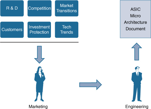
Once these questions are answered, an interaction between Marketing and Engineering takes place. Although it can be assumed this is a one-way street—Marketing asks, and Engineering delivers—it is often in reality more of a give and take, as the desires from Marketing come up against the reality of what’s possible to achieve in silicon, given the current (and ever-evolving) state of the art, cost constraints, limitations on system board space, power consumption, heat dissipation, impacts on other elements of the planned system, and many other factors.
However, after the creative process is finished, what emerges is an ASIC specification: the ASIC micro-architecture document. This document summarizes what the chip in question will do, and details how those goals will be accomplished. It is, in fact, the “blueprint” for the chip. During the lifetime of the ASIC, which may be only one generation or an evolution over several generations, this micro-architecture document is revised and updated as needed. In effect, it is the “living document” reflecting the requirements and associated design of the chip.
Once the ASIC architecture is defined, it’s time to start coding it. A present modern networking ASIC could have in excess of 1 to 3 billion transistors on it—or indeed, with the latest designs, close to 20 billion transistors. Transistors are the basic switching elements of digital circuitry—think of them as “on-off” switches for routing of electronic signals around a circuit—perfect for the binary transmissions used in computers and communications.
However, no longer are transistors visible to the naked eye. Today, a modern ASIC’s transistors are etched into a silicon wafer with element sizes of 65, 45, 32, 28, 22, or even as low as 16, 14, 10, or even 7 nanometers—billions of a meter. To put that into perspective, a human hair is about 100,000 nanometers wide, so transistors are thousands of times smaller and thinner than a human hair.
Sizes this small are very hard to grasp. So, let’s try to put that in perspective by creating our own scale. Let’s say a single human hair in cross-section is the size of the Empire State Building, as shown in Figure 7-2. On this scale, we would have to zoom up on the bottom floors of the Empire State Building to start comparing to small things. A single red blood cell on this scale stretches up to about the tenth floor. Zoom in further, and a single bacterium stretches to the third floor of our Empire State Building-sized hair width. Zoom down still (much) further, and a single strand of protein (the basic building block of a cell) is about the size of a small dog on the sidewalk, next to that giant building-sized hair cross-section.
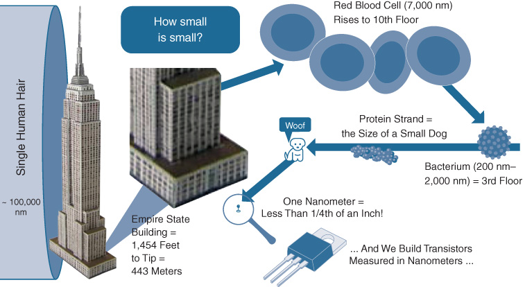
But we are still not in the realm of nanometers. To get down to that size we’d have to imagine three pennies stacked up one on top of the other, next to that Empire State Building-sized hair width. Three pennies next to that—less than 1/4th of an inch (about 6 millimeters) next to that massive Empire State Building-sized single cross-sectioned hair. That’s the size of a single nanometer.
To put it into a different perspective, an individual silicon atom is about 2/10th of a nanometer wide, so in a modern ASIC, transistor elements are being built that are only a few dozen atoms wide. This provides the capability to pack literally billions of transistors onto a single silicon die, creating the ASICs that form the heart of today’s powerful networking gear, and indeed the silicon that forms some of the most critical foundational elements in our modern technological society.
Now, here’s an interesting fact: ASICs start out as code. That may seem counterintuitive at first—hardware actually starts out as software? However, stop and think about it for a second. Do you believe that any human, or team of humans, lays out billions of transistors on a chip? It’s beyond human capability to do this, and has been for some time. ASICs actually begin their design process as software—specifically, software written in a specialized series of languages known as hardware description languages (HDLs). As indicated in Figure 7-3, two of the common HDLs that are in use within the industry are Verilog and VHDL.
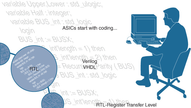
HDLs are different from standard software languages that you may be familiar with, such as C or C++, because HDLs need to incorporate things that matter at the hardware level, elements such as timing between hardware elements. ASIC designers are able to describe the actual circuits that make up various portions of the chip by coding them in a crisp and condensed form in the HDL (describing them at the hardware register level, hence the Register Transfer Level nomenclature used with HDLs).
When strung together, these portions of HDL code describe not only what the chip can do, but what form it will take when it is turned from software code into actual hardware instantiated into silicon. Basically, coding the chip takes all the items that Marketing and Engineering agreed that the ASIC needs to be able to do and expresses them as code required to drive those desired functions.
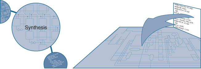
The process of synthesis is what then transforms the HDL code for the ASIC into the actual logic constructs—AND gates, OR gates, NAND gates, and the like—that make up the actual circuitry of the ASIC. Think of this as being similar to compiling a software program, only what pops out of the “compiler” in this case is not a piece of object code that you would run on your laptop computer or smartphone. Instead, the synthesis process produces what is called a netlist, which effectively is a description of what will ultimately become the physical blueprint for the chip. What starts out as software ends up as hardware. This is shown in Figure 7-4.
As it turns out, most ASICs today are of such a size and complexity that they are designed in functional blocks—one block may be for packet storage, another for processing, another for packet input/output from the chip to/from the outside world, or storage of networking policies such as security access controls lists (ACL) or descriptions of quality of service (QoS) handling, and the like. The process of arranging these functional blocks on the chip is called floor planning and placement and is shown in Figure 7-5.
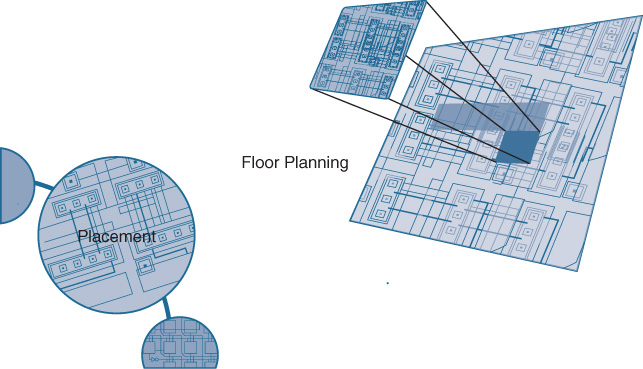
The floor planning process for the ASIC is a process that is actually done by humans—placing the functional blocks around the chip in the optimum way, interconnecting them to power, and minimizing effects between various co-located blocks such as crosstalk (an effect generated by any rapidly varying electrical field, where the associated rapidly varying magnetic field may induce unwanted interference in adjacent blocks), among other tasks. As a combination of both art and science (due to the combination of digital and analog effects at play), this step is typically done by senior engineers on the ASIC design team, and is one of the final steps as the ASIC marches toward production.
Once the netlist has been produced and the floor planning for the chip has been completed, the actual physical ASIC construction can begin. This consists of the most commonly seen elements of silicon chip manufacturing: the etching of circuit designs into silicon wafers in large, high-tech “clean rooms.” Basically (and simplifying somewhat), the chip design is physically laid out and etched using lithographic techniques onto a silicon wafer substrate, which essentially is an ultra-pure disk of silicon “doped,” or infused, with impurities of various types to enhance the silicon’s semiconductor nature in such a way as to best express the circuit’s function. Silicon is used because, as a semiconductor, it is an ideal material for switching between, and storing, digital pulses of information—the binary 1s and 0s that make up computing and communications circuitry.
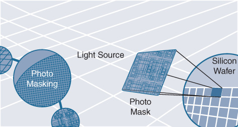
Using a combination of photolithographic and chemical techniques, the chip itself is laid out, or “photomasked,” onto the silicon wafer—typically, in multiple layers—by exposure to a high-intensity electromagnetic radiation source. To maximize production, many chips of the same type are etched onto the same silicon wafer at once, as shown in Figure 7-6.
So now, there is a wafer with dozens or possibly hundreds of our ASIC designs imprinted on it. But, do they all work? That’s the job of the next step: ASIC functional validation. The various ASIC dies now etched into the silicon wafer are individually tested. Think of this as somewhat akin to the Power-On Self-Test (POST) that your laptop undergoes when it boots up. Each silicon chip is “booted up” and run through a series of tests to determine if it is functional or not, at least at a basic level. Good chips are retained, and bad chips are marked and discarded (after the wafer is cleaved and the individual chips are apportioned out).
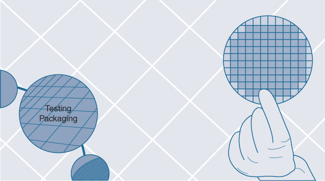
As shown in Figure 7-7, functional chips from the silicon wafer make it to the next stage, ASIC packaging, which places them into the more familiar flat, square or rectangular metal packages that we see ubiquitously on circuit boards. Again, once packaged, each ASIC is tested again, and some (which may fail during the packaging process) are discarded, while the others are retained. Figure 7-8 show the front and back of a typical packaged ASIC.
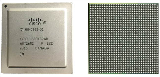
On the front of the chip, you can see various markings indicating such things as its designer, type, and point of origin. On the back, notice the ball grid array (BGA), the series of hundreds of electrical contact points by which the chip communicates to and from the outside world. This is how the chip gets soldered to its host circuit board and becomes an integral part of the system—switch, router, or other network element—that it was designed for.
Drivers of Chip Design and Density
As you are likely aware, a “law” has existed in the technology industry for the past 40 years. Moore’s law has underpinned many of the advances in technology and chip design and manufacture over the past four decades, and is thus at the fundamental root of the majority of technology advances across many diverse industries, not just computing and communications. Advances in silicon have revolutionized the world, and made possible many of the technologies used every day.
Simply stated, Moore’s law outlines that the density of transistors that can be packed onto a silicon die will double every 18 to 24 months. This has held true, more or less, for the past 40 years—and of course, this is a geometric progression—rapidly leading to very high densities that we see in today’s silicon, with billions of circuit elements.
Today, ASIC densities, as mentioned previously, may range from 65 nanometers to 45 nanometers, 32 nanometers, 22 nanometers, or even higher densities, leading to ever more complex and ever more capable chips. Basically, the smaller the transistor or circuit element, as shown in Figure 7-9, the more of them you can pack onto a chip and, hence, the more functionality the chip can provide.
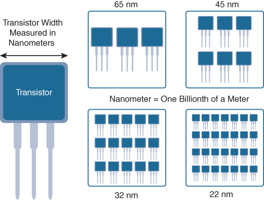
However, creating higher circuit densities in a smaller amount of space to achieve ever-greater levels of device functionality is only part of the story. Some of the key additional drivers of ever-higher chip density are shown in Figure 7-10—namely, higher performance, lower power consumption (and thus less heat that is generated and has to be dissipated), and lower cost.
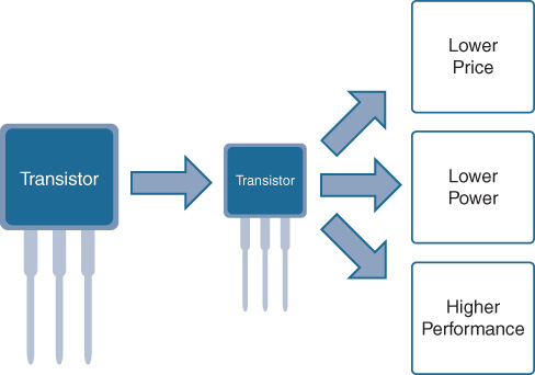
Now, at first this may seem counterintuitive. While some of the things associated with higher chip density make sense—smaller circuits consume less power, and smaller transistors and interconnections mean the electrons have less distance to travel, so speed and performance can increase—shouldn’t the cost increase as we move to an increasingly higher-tech process?
The answer is “no,” and the reason is increased yield.
Basically, all silicon wafers have impurities and imperfections associated with them. While the silicon wafer itself is ultra-pure, and great care is taken in its manufacture and use, undesired impurities or imperfections can always be present. These defects result in chips that may fail after the photomasking step, resulting in chips that have to be discarded after testing, as shown in Figure 7-11.

The fraction of chips that are manufactured correctly and operate properly versus the failed ones is called the yield for the silicon wafer in question. The cost to manufacture a given chip is directly related (among other factors) to the yield achieved by the wafer manufacturing process. The higher the yield, the lower the per-chip cost. This makes sense intuitively when you consider that manufacturing a smaller version of the same chip (by going to a higher-density chip manufacturing process—45 nm versus 65 nm, say) makes it statistically less likely that any individual chip on the wafer will be masked over a “problem” area on the die, versus a larger version of the same chip design. An example of this is shown in Figure 7-12.
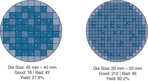
Basically, the smaller the chip, the higher the typical yield. The higher the yield, the lower the per-chip cost (as there is a greater proportion of “good” chips that can be used versus “bad” ones that must be discarded). Of course, many other factors come into play concerning chip costs—the maturity of the given silicon “process node” (65 nm, 45 nm, 32 nm, 22 nm, 16 nm, 10 nm, etc.) being one—but all things being equal, smaller is typically better in terms of performance, power consumption, and cost.
As this book goes to press, the state-of-the-art in the industry is leading to the construction of chips at the 7 nm process node. Various additional factors, such as the capability to build up transistors on the silicon die in three dimensions rather than two, also lead directly to ever-greater transistor packing densities and efficiencies in chip design and manufacture. The technology involved is amazing, when you stop to think about it, and is the basis for many of our ever-greater technological capabilities and advances.
When Good Chips Go Bad: What Can Go Wrong in Chip Design
Remember that silicon hardware actually starts off as software? Well, like any software, chip designs can have bugs. The difference is, these bugs might get caught early in the design process—but on the other hand, they might not actually be found until the chip goes through the whole design and manufacture process, and you get the first chip back and place it onto a board to test it out.
This is a big moment for the ASIC team! The first batch of their ASIC comes back from the manufacturer, gets soldered onto the logic board, and the first load of software gets turned up to test not just that chip, but the system into which it is embedded, and of which it is a part. Does it work as intended? Does it meet all performance and functional specifications?
Figure 7-13 shows the whole lifecycle of an ASIC design process, from coding, synthesis, and floor planning, through manufacture and packaging, into system testing. If everything works, on to the next steps. But there is always the chance of a bug or unforeseen issue with the chip, which may only emerge during whole-system or unit testing.

Depending on what is wrong, it may be possible to work around the issue in hardware or in software. If not, it’s time for a respin. ASIC respins involve identifying the issue and then stepping back through the process to fix the problem, which may have been introduced, for example, at the coding or floor-planning stages. ASIC respins are as costly and time-consuming as you might expect, and are compounded by the fact that at this point in the project, other teams (software, system test, etc.) may be waiting on having a functional ASIC. While some issues can be found and fixed in simulation before the ASIC is physically produced, others may be possible to find only after production. Needless to say, ASIC respins are undesirable.
When Good Chips Need to Get Better: Designing the Next Generation
In addition to the respin scenario covered in the previous section, there are other reasons for an ASIC respin. After an ASIC has had a given period of time and success in the market, the ASIC designers may want to revisit the design of the ASIC and add or modify its underlying functionality. Maybe the market has changed, new protocols have come along, or customers want new functionality, capabilities, or scale that differs from what the initial ASIC offered.
When revisiting the ASIC design, depending on what’s needed, the code for the ASIC typically is modified, and then the entire chip design process kicks off again, resulting in a new version of the ASIC in question. This process, sometimes also (somewhat confusingly) called a respin, ends up yielding the next generation of the ASIC involved.
If this is examined in Cisco switching, you can see this process playing out over many chip generations. One of the longest-lived switch ASIC families in Cisco history is the EARL series of ASICs—EARL being an acronym for Encoded Address Recognition Logic. As a chip design, EARL actually started its life in the Catalyst 5000/5500 Series switches—the precursor to the Catalyst 6500/6800—and has in fact made its way into the Nexus 7000/7700 Series switches as well.
As depicted in Figure 7-14, the EARL series of ASICs has now played out over eight generations—with each EARL generation increasing in density, functionality, and performance. Today, the EARL8 ASIC used in the Catalyst 6500, 6800, and Nexus 7000 M-Series line cards provides a wide range of advanced networking capabilities, including IPv4 and IPv6 forwarding, Multiprotocol Label Switching (MPLS), Virtual Private LAN Services (VPLS), Overlay Transport Virtualization (OTV), Generic Routing Encapsulation (GRE), Advanced IP Multicast, Encapsulated Remote Switched Port Analyzer (ERSPAN), NetFlow, Virtual Switching System (VSS), and a host of additional advanced functionality. With a lifespan approaching 20 years, and widespread customer acceptance of the platforms it is integrated into, Cisco’s EARL technology represents one of the most prolific and widely used network fixed-function ASICs in the networking industry.

Now We Speak the Same Language!
Now you know how chips are made. Chip design is based on planning, synthesis, and manufacturing. You now have the basis for appreciating the differences between various types of networking silicon—and specifically to start understanding why flexible, programmable silicon plays such a big role in today’s, and tomorrow’s, network infrastructures.
Now, let’s begin with the big trends in networking today, and how innovations in Cisco’s advanced networking silicon—forming the foundation of Cisco Digital Network Architecture—are responding to those trends and creating the basis for the next big leaps in networking.
What’s Happening in the World of Networks
Today, networking is changing faster than ever before. Why? Because business is changing faster than ever before.
This is a period of digital disruption. Long-established businesses are augmented (or obsoleted) seemingly overnight. New technologies spring up, opening up new possibilities that were previously infeasible, or even impossible. And all of this is happening at a pace that would have seemed unimaginable even a few years ago.
Look at Amazon. Consider Uber. And then think about the next area of our lives that might be headed for disruption in the new digital era.
What this means for networks is that they have to respond faster to the business, and not just in terms of megabits or gigabits. A network needs to be more adaptable—more agile—and more open to new innovations, be they in protocols, in capabilities, or in solutions.
An example of this is software-defined networking (SDN). Originally conceived at Stanford as part of its Clean Slate Program, SDN has since transmuted into many forms, including OpenFlow, overlays, and orchestration, among others. But whatever form SDN takes, or whatever set of capabilities it requires, chances are very good, as shown in Figure 7-15, that the resulting set of functional requirements needs to be expressed into network hardware—the silicon that powers the switching and routing infrastructure of the enterprise network.
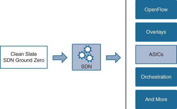
And yet this seems to be at odds with the areas just examined around the development of ASICs and silicon. The average amount of time from white-boarding out a new set of ASIC requirements to having that “first piece of silicon” that meets those requirements (the whole process just examined) is typically 18 to 24 months, and could be even longer. And yet, this is an era where requirements, capabilities, and technologies might morph in a period of months—and when new industry trends like SDN arise that need to be addressed.
How Traditional Network ASICs Process Packets
To examine how Cisco’s innovative approach to flexible silicon with Cisco DNA addresses this issue, let’s review how an ASIC (such as the ones examined earlier in this chapter) processes network packets.
A network ASIC is hard-coded (remember HDLs?) to perform a specific set of functions on packets it processes. These include the following:
Parsing the packet (What kind of packet is this? IPv4? IPv6? MPLS? etc.)
Layer 2 lookup
Layer 3 lookup
Policy actions such as filtering (ACLs) and QoS
Packet modifications (Time to Live [TTL] decrement, L2 rewrite)
Packet scheduling
Statistics gathering
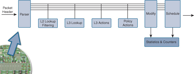
All packets that arrive at the network ASIC are handled in a processing pipeline, which applies the necessary steps in the correct order. It is this pipeline that is established by the network ASIC’s HDL code, and laid down in its hard-wired silicon gates.
When a packet arrives at a network ASIC, the first step is to parse the packet to see what type of packet it is, so that the subsequent stages within the ASIC can process it appropriately. This involves examining the various packet headers, and creating internal “metadata” about the packet that can be passed from ASIC stage to ASIC stage as the packet gets processed and handled.
If a typical network ASIC needs to parse and process a type of packet it is not hard-coded to handle, it cannot. An example of this is the ASIC that powers a Catalyst 3750 switch. This ASIC parses IPv4 and IPv6 traffic, but has no capability to parse MPLS traffic. Lacking this hardware capability at the ASIC level, it is not possible to add MPLS support to a Catalyst 3750 switch. Sending all traffic that matches MPLS (unknown-to-the-switch protocol) up to the switch’s control-plane CPU introduces such a processing burden, and results in such a poor level of throughput that this is not an option (think a few thousand packets per second [pps] at best, versus millions of pps the chip can process in hardware). So, protocols that are unknown to the switch (which the fixed parser block of the ASIC cannot understand) are typically simply dropped in hardware because they cannot be processed.
Thus, it can rapidly be seen, as depicted in Figure 7-16, that the traditional fixed processing pipeline of a network ASIC, while functional, lacks flexibility.
So how can today’s organizations handle rapid network change? What happens when new protocols come along? What if the business needs to adopt new solutions, and those new solutions require new and different capabilities in the network?
Enter flexible silicon, a key component of Cisco Digital Network Architecture.
Beginning several years ago, Cisco pioneered the development and use of flexible network ASIC silicon with Unified Access Data Plane (UADP), the world’s first fully flexible and programmable piece of switching silicon, and QuantumFlow Processor (QFP), a remarkable piece of flexible, programmable routing silicon.
The latter half of this chapter explores UADP and QFP in detail to help you understand the extraordinary capabilities that they provide, and why this set of capabilities matters for your business.
You might be saying to yourself, “What about CPUs? What about FPGAs? Don’t they provide flexibility? Can’t they be used for packet forwarding? How do they fit into this picture?”
So, let’s cover that first.
Traffic Handling with CPUs and FPGAs
For lower-performance applications, you can certainly use a traditional CPU (x86 Intel or other) for processing packets. The flexibility a CPU provides for packet processing is excellent, and with the right software stack on top, a CPU can do almost anything for network traffic handling.
But the performance is limited. Why? Well, CPUs are not at all optimized for the types of things that get done every day—indeed, every microsecond—in networks. After a packet is parsed, it gets looked up in tables—all sorts of tables. Layer 2 lookups, Layer 3 lookups (including exact-match as well as Longest-Prefix match), ACL lookups for security and traffic filtering, QoS lookups for traffic classification, NetFlow table lookups…the list goes on and on. And every lookup has a different data structure, a different set of requirements, and a different possible outcome for the packet involved.
CPUs can certainly do this work. However, all the tables they are accessing exist “off-chip”—that is, in memory located outside of the CPU. Thus, every lookup incurs a performance penalty as data is shuttled between the CPU and the external memory. A single lookup for a packet could involve many memory accesses, and a single packet might incur many lookups. So, beyond a relatively modest performance level (typically, a few Gbps), CPU-based packet forwarding implementations tend to “top out” in the real world, where multiple packet-processing functions are required. The high-end CPUs required to obtain such performance levels also tend to be quite expensive, especially when examined through the lens of cost per bps moved. Larger CPUs also often involve higher levels of power consumption and heat generation/dissipation, issues that introduce additional challenges in system design for network devices.
So, as shown in Figure 7-17, CPUs get top marks for flexibility, but tend to not do so well at cost and performance.
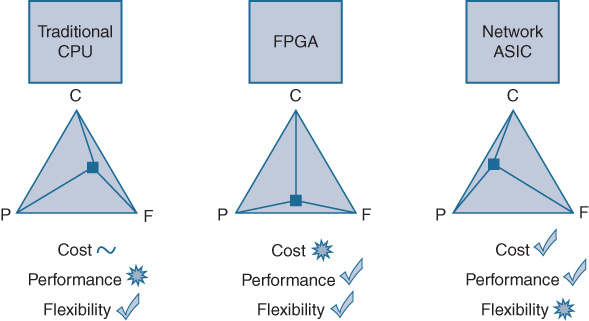
Next up are field-programmable gate arrays (FPGA), specialized pieces of silicon that contain a number of programmable logic blocks, connected together by a set of reconfigurable logic elements such that an FPGA can, with the right software coding, be made to do many things that a traditional hard-wired ASIC could accomplish. FPGAs thus provide some of the same levels of flexibility that a CPU might, but at a higher performance level that is more comparable to the performance of a traditional network ASIC.
The downside to FPGAs is typically cost and complexity. On a cost-per-bps-moved basis, an FPGA tends to be an order of magnitude more expensive than a comparable network ASIC, because an FPGA is not optimized for any particular task, and again often lacks the on-chip memory needed for packet lookups (thus requiring augmentation with additional chips). Forming a middle ground between CPUs and ASICs, FPGAs are sometimes used as “gap fillers” in platform designs—helping to augment a traditional ASIC, which may lack one or two key functions, to fulfill a particular set of design objectives.
An example is Virtual Extensible LAN (VXLAN) support on the Catalyst 6800, where the EARL8 ASIC that forms the Catalyst 6800’s forwarding engine supports many diverse protocols, but lacks support for VXLAN processing capability (as EARL8 was developed prior to VXLAN’s debut into the market). In this case, front-ending the EARL8 ASIC complex with an FPGA to handle VXLAN can provide the required functionality—while the EARL8 chipset continues to process all other, non-VXLAN-encapsulated traffic flows (or traffic flows from which the VXLAN header has already been pushed/popped).
FPGAs are typically too expensive, however, to be used for the entire set of required packet-forwarding and traffic-handling functions in most platforms. Which brings us back to the traditional network ASIC, which provides excellent performance at a very reasonable cost (due to its fixed nature) but lacks the flexibility to handle new protocols and capabilities as they arise.
So, it seems like none of these are ideal for network traffic handling in our new, software-defined era…that there is no perfect answer, as shown in Figure 7-17.
Is there a better answer, one that provides the optimum balance between performance, flexibility, and cost? One that is ready to support the networking protocols and capabilities of today, and be flexible enough to handle the demands of tomorrow—even demands that may not be known yet?
Enter Cisco’s flexible silicon to support Cisco DNA: UADP and QFP.
Introducing Flexible Silicon
The “holy grail” of flexible silicon is to provide all of the following:
The programmability and flexibility approaching that offered by a CPU
The performance equivalent to that of a hard-wired network ASIC
The lowest possible cost
By correctly balancing all three of these factors, a truly flexible piece of silicon—a programmable network ASIC—can provide an unparalleled set of capabilities in today’s (and tomorrow’s) network infrastructures, as depicted in Figure 7-18.

How can this balance be achieved? The key is by introducing microcode programmability and flexibility to the various stages in the network silicon processing pipeline. By doing so, these processing stages can be adapted over time to handle new protocols and new capabilities, in support of new network solutions.
The method used to adapt the flexible ASIC to these new capabilities as they arise is to download new microcode into the chip. This is typically done when the platform involved boots up, and the flexible network ASIC is programmed with the latest set of microcode (bundled as part of the platform’s OS). As shown in Figure 7-19, the network operator can load a new version of software onto the box—reload—and get a whole new switching and routing functions on the platform involved. This is an excellent method of investment protection, allowing the network device to adapt to new needs and capabilities over time, and serves to illustrate the power of flexible hardware.
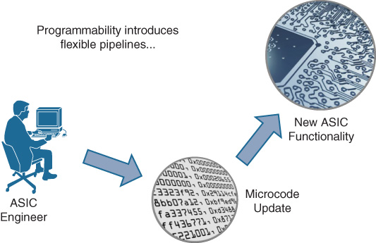
Once the new microcode is loaded, some, most, or even all of the stages of the flexible network ASIC gain new levels of functionality—handling new protocols, providing new sets of capabilities—doing it all at a cost associated with a more traditional hard-wired network ASIC, thereby making these sophisticated functions available at price points that allow widespread and pervasive use within the network. Figure 7-20 shows an example of a flexible ASIC in action.
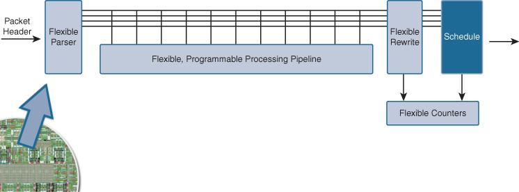
The crucial distinction here is that a truly programmable ASIC provides this type of flexibility at a cost point that other technologies (such as FPGAs) cannot—and at a performance point well in excess of what any CPU could achieve.
Flexible ASIC technology is truly the key to the next generation of networking. Cisco pioneered the use of flexible ASIC technology in high-volume enterprise switching platforms when it introduced the Catalyst 3850 switch platform to the market in early 2013.
Flexible Switching Silicon: UADP
If you have ever used a Catalyst 3850, 3650, or 9000 Series switch, or passed traffic through one, you have used UADP.
The Cisco Unified Access Data Plane ASIC is a premier example of flexible switching silicon. Consisting of multiple generations of chips ranging from 1.3 billion to over 3 billion transistors—and now up to almost 20 billion transistors in its latest versions—UADP is one of the most complex, sophisticated, and impressive pieces of switching silicon anywhere in the world.
UADP began in 2013 as a key component in the then-brand-new Catalyst 3850 switch platform, and is the result of over five years of planning and design work prior to that, encompassing dozens of Cisco ASIC engineers and software and hardware designers. Today, UADP is used in the Catalyst 3850 and 3650 platforms, the Catalyst 4500 Supervisor 8-E and 9-E, and the Catalyst 9000 Series of fixed and modular switch platforms.
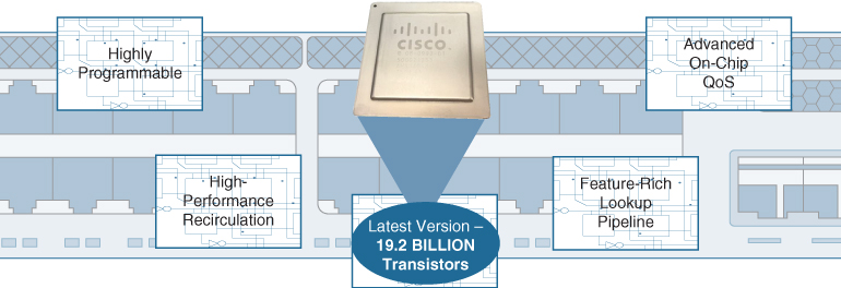
As a quick overview, some of the highlights of UADP are summarized in Figure 7-21 and examined in the subsequent list.
UADP highlights are as follows:
Highly programmable: UADP offers an unparalleled level of flexibility, by introducing a Flexible Parser block (capable of looking up to 256 bytes deep into the packet header), combined with a series of flexible, programmable packet-handling stages for handling the packet once parsed. With a total of 22 programmable stages (15 ingress, 7 egress) in the original UADP 1.0, and 25 programmable stages in the latest UADP 2.0 and 3.0 versions, UADP provides flexibility like no other ASIC in its class.
Advanced on-chip QoS: Quality of Service is critical in enterprise networks, as the network strives to separate mission-critical, delay-sensitive traffic from other bulk traffic streams. UADP provides a set of comprehensive set of QoS capabilities, providing excellent traffic-handling flexibility.
High-performance recirculation: All of the really interesting new capabilities in networking involve some sort of tunnel (defined as adding/removing a tunnel header in front of the existing packet header as provided by a user or device). Examples of such tunnels include MPLS, GRE, VXLAN, and many other protocols. UADP was created with tunneling in mind. Tunneling a packet involves a capability called recirculation—basically, feeding the newly encapsulated or newly decapsulated packet around for a “second pass” through the ASIC, necessary to handle the newly inserted or removed header for appropriate traffic handling and forwarding. As you will see, UADP is optimized for recirculation, and is thus primed for handling the newest and latest advances in networking as they arrive.
Feature-rich lookup pipeline: All of the flexible, programmable stages in UADP can perform zero, one, or two lookups against a packet being processed—and all of the tables being referenced are on-chip, keeping performance consistently high. The result is a lookup pipeline that can provide many features to a packet in a single pass—and can provide multiple passes on a packet if required, for the maximum in feature processing as required by today’s increasingly sophisticated network traffic handling.
High-density, powerful, flexible silicon: 1.3 billion transistors per chip. Impressive in something that’s smaller than your fingernail, isn’t it? That was for the very first generation of UADP, version 1.0. The latest versions of the UADP ASIC now packs 3 billion transistors (UADP v1.1, as used in the Catalyst 3850/3650 Multigigabit Ethernet [mGig] switches), 7.46 billion transistors in the UADP 2.0 ASIC (as used in the Catalyst 9000 Series switches), or up to 19.2 billion transistors in the very latest UADP 3.0 ASIC (as used in the Catalyst 9000 25Gbps/100Gbps switches). And, all UADP ASICs are designed for flexibility as well as performance.
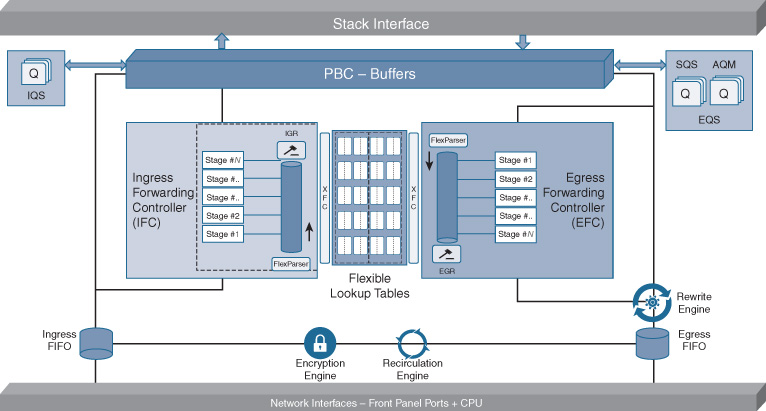
Let’s examine UADP more deeply by first looking at a block diagram of the chip. Some of the key areas are shown in detail in Figure 7-22.
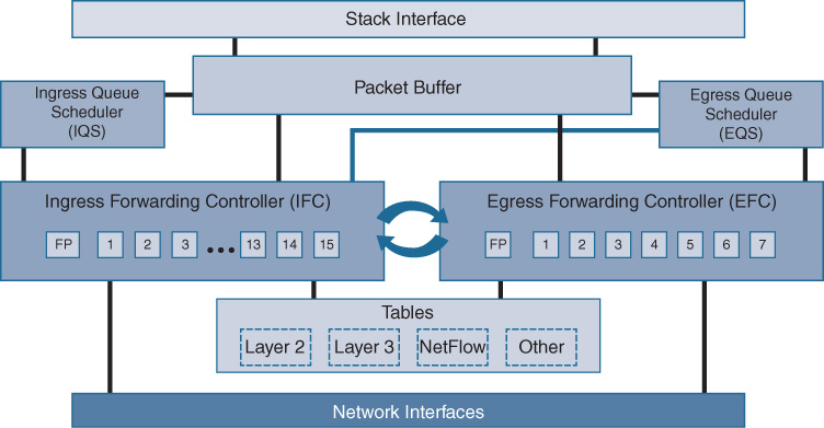
On the bottom of the diagram, the network interfaces are Ethernet ports (operating at various speeds) that you may attach devices to on the switch. These feed directly into the first key element of the UADP ASIC, the microcode-programmable Flexible Parser (FlexParser), as shown in Figure 7-23, housed within the UADP’s Ingress Forwarding Controller (IFC).
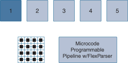
The FlexParser is key to the flexibility and adaptability to new protocols and functions that UADP provides. The FlexParser allows UADP to be adapted to understand, and allow to be processed, new protocols and new capabilities over time.
The FlexParser sits at the front of the IFC, which contains a total of 15 (UADP 1.0/1.1) or 17 (UADP 2.0/3.0) flexible, programmable stages for processing of packets identified and classified by the FlexParser block. This is shown in more detail in Figure 7-24.
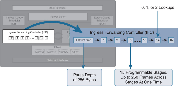
The UADP ASIC’s FlexParser can be programmed, via microcode, to handle many different packet types and encapsulations. At the time of writing, UADP has already been microcoded to handle the following key networking protocols, among others:
IPv4
IPv6
GRE
MPLS (L3 and L2 VPN)
VXLAN
Critically, UADP can be programmed in the future for many other encapsulations, if and when the need for them arises. This includes encapsulations that have not necessarily even been invented yet. As of IOS-XE 16.3, the UADP ASIC in the Catalyst 3850, 3650, and 9000 Series switches handles VXLAN encapsulation. The VXLAN protocol, documented as RFC 7348, was invented after the UADP silicon was designed and built—and yet, the adaptable nature of UADP’s FlexParser allows, via a simple software upgrade, for VXLAN traffic to be understood and processed, with high performance, in UADP’s programmable hardware pipeline.
UADP’s FlexParser can parse up to 256 bytes deep into the packet, allowing almost any protocol, current or planned, to be handled (requiring only the necessary microcoding, and associated higher-level software, for traffic handling). The ability in UADP to keep many packets in flight simultaneously (up to 250) keeps performance consistently high, and enables the impressive throughput numbers associated with succeeding generations of UADP as follows:
UADP 1.0 (used in Catalyst 3850/3650 1G copper): 56 Gbps
UADP 1.1 (used in Catalyst 3850 mGig and 10G fiber): 160 Gbps
UADP 2.0 (used in Catalyst 9000 Series switches): 240 Gbps
UADP 3.0 (used in the Catalyst 9000 Series 25G/100G switches): 1.6 Tbps
Once a packet makes it through the IFC, it’s off to the Ingress Queue Scheduler (IQS). This is the portion of UADP that handles ingress packet queueing. The packet itself is placed into the packet buffer (6 MB on the original UADP, as used in the Catalyst 3850 and 3650 1G-copper platforms, and up to 16 MB and 32 MB/36 MB, respectively, in the Catalyst 3850 mGig/10G Fiber platforms and the Catalyst 9000 Series platforms). The IQS determines which packets receive priority for handling either into the stack interface (between switches) or to other front-panel ports.
Once the packet’s turn arrives to be forwarded, it is sent along to the Egress Forwarding Controller (EFC), where it can undergo up to another seven programmable stages (UADP 1.0/1.1) or eight programmable stages of handling (UADP 2.0/3.0) on the egress side of the chip, for additional packet-processing flexibility. Once the packet passes the EFC, it is in turn scheduled out of the ASIC—and sped along into the outside world—via the Egress Queue Scheduler (EQS), ensuing appropriate traffic handling for all traffic flows.
All of the tables—Layer 2, Layer 3, NetFlow, etc.—that UADP needs to reference for traffic handing are located on-chip for maximum performance, which allows UADP to provide excellent performance even when many diverse functions and lookups are being performed on any given packet flow. Lookup bus bandwidths are up to 512 bits wide, meaning that lots of data can shuffle back and forth very rapidly and, when combined with the packet-handling rate of UADP, that the chip contains literally terabits’ worth of internal bandwidth, as shown in Figure 7-25.
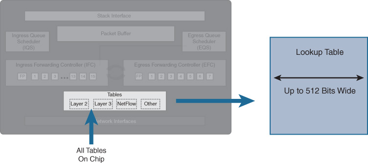
Along the way, all of the necessary packet-level and flow-level statistics, including counters, full-flow NetFlow, and other information, are gathered and logged. UADP includes the capacity for tens of thousands of NetFlow entries (with capacity varying by UADP version), tracking statistics and usage on every single packet traversing the platform—critically important in today’s networks, where keeping close track of all traffic flows is important for new and emerging network security applications, as well as more traditional capacity planning and network usage accounting functions.
Should recirculation be required—which it will be if tunneling is involved—UADP performs exceptionally. Tunneling requires recirculation because, when a tunnel header is added or removed, the packet’s destination has by definition changed, and so a recirculation (passing the packet through the ASIC’s processing pipeline again) is necessary to forward the traffic to the “new” encapsulated or de-encapsulated destination, along with all the policies that need to apply to the packet.
The UADP’s recirculation latency (the time required to get a packet off the end of the EFC’s egress pipeline, and back to the front of the IFC’s ingress pipeline) is sub-microsecond, clocking in at approximately 500 nanoseconds. That’s 500-billionths of a second, or about 1/700,000th of the time it takes you to blink your eye. When combined with massive recirculation bandwidth (because bandwidth not being used by the front panel ports is available for recirculation, along with dedicated recirculation bandwidth as well), this means that traffic recirculation, when required, poses no issues for UADP. This is shown in Figure 7-26.
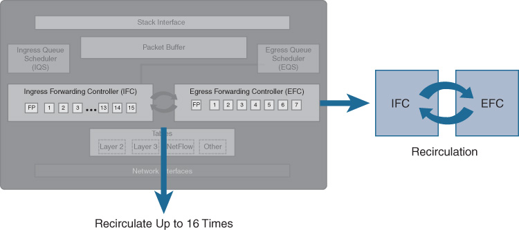
For maximum flexibility, packets can be recirculated between the IFC and the EFC up to 16 times, allowing for any currently conceivable packet-handling requirements. At the present time, no use case exists for more than seven recirculations, but it’s nice to know that the UADP hardware provides the flexibility for more in future, should this be required.
The second key element of UADP is the ability to connect to an extremely high-performance stacking interface, which is used to connect multiple UADP ASICs together in a system (multiple chips in one box and/or multiple boxes combined in a stack), as shown in Figure 7-27.
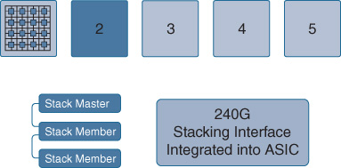
The UADP stacking interface in the Catalyst 3850 operates at 240 Gbps and consists of three counter-rotating stack rings operating at 40 Gbps apiece. By incorporating a function known as Spatial Reuse (which allows recovery of unused bandwidth on the stack ring by destination stripping of unicast traffic from the ring), an effective doubling of stack ring bandwidth can be achieved, boosting stack performance up to 480 Gbps.
The Catalyst 3850 stack ring architecture (known as StackWise Plus) is shown in Figures 7-28 and 7-29, which depict multiple switches connected together in a stack; this architecture enables the stacked switches to behave as a single unit (that is, a single switch) for the purposes of configuration as well as network Layer 2/Layer 3 topology.

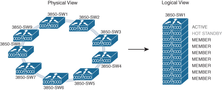
The Catalyst 3650 provides a “single lane” of stacking bandwidth, versus the Catalyst 3850’s “three lanes,” limiting 3650 stacking performance to a still very respectable 160 Gbps with spatial bandwidth reuse. The high performance of the Catalyst 3850/3650 stack, when combined with QoS which is stack-aware, ensures that inter-switch connections in a Catalyst 3850/3650 stack are never the bottleneck for traffic flows in the network.
This same stacking ring architecture is also present in the Catalyst 9300 Series switches, where it is used to connect up to eight Catalyst 9300 switches together in a StackWise Plus ring. In addition, this stacking architecture is also used on the Catalyst 9400 modular switch’s Supervisor Engine, as well as on the Catalyst 9500 Series switches (where the ring is used to connect multiple ASICs together to provide forwarding for and across the entire switch). In these latter two cases (Catalyst 9400 and 9500), the internal stacking ring bandwidth between ASICs is increased to 720 Gbps for maximum performance.
Selected Catalyst 9000 Series switches also support StackWise Virtual capability, which allows for stacking interconnection of switches via front panel ports, providing enhanced flexibility and resilience.
The next major benefit of UADP is its integrated on-chip Micro Engines for fragmentation and for encryption/decryption, as shown in Figure 7-30.
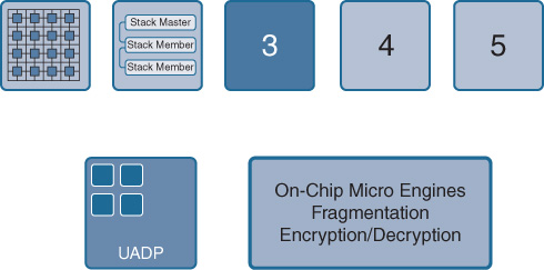
Certain functions are always known to be common in networking, and at the same time known to be large consumers of processing power and bandwidth. These include fragmentation (common when any tunneling protocol is in use), as well as encryption and decryption.
By providing purpose-built areas within the UADP silicon dedicated to these functions, no cycles within the programmable pipeline are consumed for these processing-intensive capabilities. This preserves bandwidth and ensures that performance is kept consistently high, while also preserving microcode space within the UADP’s programmable pipeline for other functions and capabilities.
Having high-performance fragmentation support—in hardware—on UADP is especially critical, considering how many of today’s advanced networking functions leverage tunneling capability, and thus may need access to this high-performance packet fragmentation engine (for example, when the egress maximum transmission unit [MTU] size on an output interface is exceeded in the event that an encapsulation header is added to the packet involved).
In terms of encryption support, newer versions of the Catalyst 3850 platform (those with mGig ports) as well as the Catalyst 9000 Series switches also incorporate Media Access Control Security (MACsec) capability, for additional link-layer security. MACsec operates in these platforms at line rate and offers an excellent capability for port-level encryption of sensitive data, using robust encryption standards up to AES-256 with Galois Counter Mode (GCM).
The fourth key capability within UADP is high-performance packet recirculation. As mentioned previously when discussing the IFC and EFC, recirculation is a key element when handling tunneled traffic, which requires encapsulation/decapsulation, and this needs more than one pass through the ASIC prior to, or following, tunnel encapsulation/decapsulation. This is shown in Figure 7-31.

The extremely low recirculation latency, and highly optimized recirculation path, in UADP provides for excellent handling of tunneled traffic flows, and ensures that today’s, and tomorrow’s, tunneled protocols can be handled efficiently.
The fifth and final key element provided by UADP is integrated, on-chip full-flow NetFlow for traffic visibility, as shown in Figure 7-32.
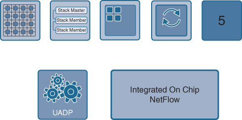
By providing NetFlow capability on every single packet that transits the switch, UADP provides excellent traffic visibility for accounting, capacity planning, security, and other purposes. The NetFlow table capacity offered by UADP—24,000 entries per UADP 1.0/1.1 ASIC, increased to higher capacities in following versions of UADP—is an excellent match for UADP’s intended role within the switched network infrastructure of an organization.
Taken together, the five key capabilities of the UADP ASIC provide for unparalleled traffic-handling capability, flexibility, and power are as follows:
Microcode-programmable FlexParser, with 15-stage programmable ingress pipeline and 7-stage programmable egress pipeline (increased to 17 ingress stages and 8 egress stages in UADP 2.0 and 3.0)
Integrated extremely high-performance stacking capability
On-chip Micro Engines for fragmentation and encryption
High-performance recirculation (extremely low recirculation latency and high recirculation bandwidth)
Integrated on-chip NetFlow (full-flow)
UADP Use Cases—Current, and Future
The UADP ASIC offers several key use cases, all implemented in currently available code. These include advanced QoS, support for MPLS VPNs, and support for VXLAN tunneling and Scalable Group Tags (SGT).
As shown in Figure 7-33, the advanced QoS capabilities of UADP include support for Approximate Fair Drop (AFD), an advanced QoS algorithm that ensures fairness among multiple competing sources for network traffic, especially when those traffic flows include low-bandwidth (mice) flows contending with high-bandwidth (elephant) flows in the network. AFD is designed to ensure appropriate QoS traffic handling to both types of flows, allowing them to coexist on the same network gracefully.
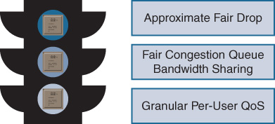
When combined with Fair Congestion Queue Bandwidth Sharing and Granular Per-User QoS, UADP offers excellent options for ensuring that traffic is handled in accordance with existing best practices as well as enterprise QoS policies.
Today, many organizations wish to avail themselves of the capability to introduce segmentation into their network topologies. This may be done, for example, to provide enhanced security by reducing the total network attack surface available to a malicious actor or rogue network device. With the requirement to support such advanced network segmentation on UADP, the ability to handle the appropriate network segmentation technologies such as MPLS VPNs for topology-oriented segmentation or SGTs for topology-less segmentation/micro-segmentation became key.
In addition, the use of newer technologies such as VXLAN serve to enhance the range of available network segmentation solutions available to the network designer and manager. Thanks to the flexible, programmable nature of the UADP ASIC, these capabilities were added via a simple IOS-XE software upgrade on the existing Catalyst 3850 and 3650 platforms, and are also available on Cisco’s new Catalyst 9000 Series switches.
As mentioned, an excellent example of the flexibility provided by UADP is support for the VXLAN protocol. VXLAN is a key protocol for supporting the use of fabric-based network capabilities within the enterprise network, as provided by the Cisco Software-Defined Access (SD-Access) solution. The flexible nature of VXLAN encapsulation, which can support both Layer 2 and Layer 3 encapsulated payloads, is critical for use in tomorrow’s flexible network fabric infrastructures.
A quick examination of the VXLAN protocol is provided in Figure 7-34.
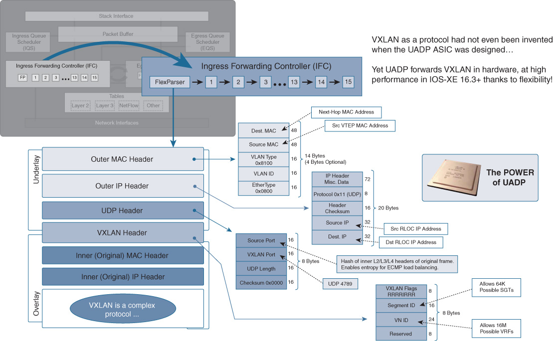
It is interesting to note that the UADP ASIC was designed before VXLAN as a protocol had even been invented, yet UADP forwards VXLAN traffic, in hardware, with high performance. Stop and think about that for a second. UADP was created before VXLAN was even invented, yet UADP supports VXLAN traffic forwarding and manipulation in hardware. This is the true power of flexible silicon—the ability to handle new protocols and new functions as they come along, flexibly adapting to new trends and requirements in the networking industry without having to replace the underlying hardware. This is an extremely powerful capability in the flexible silicon produced by Cisco, one which enables significant investment protection for customers, now and into the future.
Introducing the Future: UADP 2.0 and 3.0
UADP 2.0 and 3.0 are the latest and (so far) greatest member of the Unified Access Data Plane ASIC family. These new UADP versions continue the legacy of flexibility pioneered by the UADP versions that preceded them, and at the same time add critical new functionality and performance to enable the next generation of switching platforms, and the capabilities they provide.
A quick comparison of the various UADP models is provided in Figure 7-35.
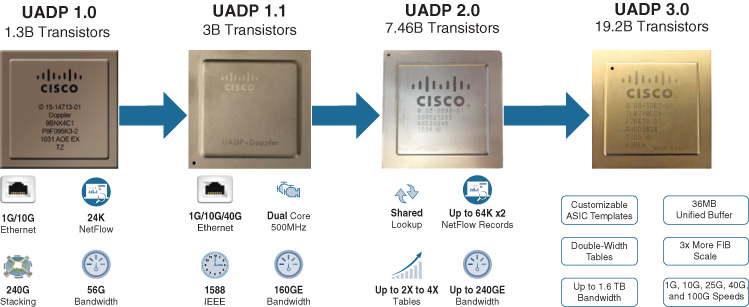
The original UADP 1.0 ASIC was a very capable piece of silicon. Supporting 1G and 10G Ethernet, 56-Gbps processing bandwidth, an integrated 240-Gbps stacking interface, and up to 24,000 NetFlow records (full-flow, not sampled), UADP 1.0 formed the basis for the first Catalyst 3850 and 3650 platforms and offered great performance as well as flexibility. Produced in both 65-nm and 45-nm sizing, UADP 1.0 packaged all of this into 1.3 billion transistors’ worth of packet-processing goodness.
UADP 1.1 built on top of the capabilities of 1.0, retaining UADP’s hallmark flexibility and adding support for 40G Ethernet, IEEE 1588 precision timestamping, and up to 160 GB of total bandwidth. By moving to a 28-nm production process, UADP 1.1 squeezed two processing cores onto a single silicon die operating at a higher clock rate, further increasing performance—necessary to keep up with the vastly increased port densities and port speeds provided by the new Catalyst 3850 10G fiber switches and the Catalyst 3850/3650 mGig (100M/1G/2.5G/5G/10G) platforms.
UADP 2.0 and 3.0 are the latest variations of UADP. UADP 2.0 forms the foundation for the new Catalyst switching platforms—the Catalyst 9000 Series family, consisting of the Catalyst 9300 stackable switches, the Catalyst 9400 modular switches, and the Catalyst 9500 fixed-configuration core switches. UADP 3.0 is used in the higher-end Catalyst 9500 switch platforms—those employing integrated, high-density 25G and 100G Ethernet ports.
UADP 2.0 and 3.0 support a number of important additions to the set of capabilities already provided by the other UADP family members. These include an increase in bandwidth to 240 Gbps and 1.6 Tbps capacities, respectively (leveraging multiple cores at higher clock rates within a single ASIC to deliver higher overall capacity), an increase in the NetFlow table size supported, and an increase in other table sizes (Layer 2, Layer 3, etc.) anywhere from two to four times compared to previous UADP generations. As well, the total number of counters in the UADP 2.0 and 3.0 ASICs is substantially increased from previous generations, leading to a richer ability to generate statistics—very useful for next-generation analytics and related capabilities for traffic flow analysis.
In addition, one of the most important innovations provided by these latest generations of UADP is arguably their ability to provide flexible lookup table capability, enabling UADP 2.0 and 3.0 to flexibly reallocate these tables as needed for the particular job at hand, and share their packet-processing tables between the various areas within the UADP ASIC itself. This is shown in Figure 7-36.
Why is this flexible lookup table capability important? Recall that everything in networking typically involves table lookups. However, the exact sizing of the lookup tables needs to vary according to the task at hand. For example, an access-layer switch may need more entries for MAC addresses (because it is Layer-2 adjacent to a large number of hosts), while a core switch may need more Layer 3 Forwarding Information Base (FIB) entries or NetFlow entries, because it is handling more traffic in aggregate and is exposed to a larger total routing domain.
UADP 2.0 and 3.0 are excellent for this use because their table sizing can be adjusted between various functions under software control. Depending on the platform and its network role, UADP 2.0 and 3.0 can be configured for a larger or smaller number of table entries for various given areas—unicast Layer 3, multicast Layer 3, Layer 2, NetFlow, security ACLs, QoS ACLs, and so forth. Within the chip, these are all handled as either ternary content-addressable memory (TCAM) or static random access memory (SRAM) resources, whose size can be modified as needed. This flexibility offers an excellent ability to customize the actual packet handling of the network switch incorporating UADP 2.0 or 3.0, in accordance with its role and placement within the network.
In addition, UADP 2.0 and 3.0 utilize shared lookup tables that can be accessed across both processing cores within the ASIC. This innovation conserves TCAM space by allowing both processing cores within the ASIC to access a single copy of a programmed table entry, thus avoiding having to program such an entry twice and providing maximum scalability without compromising performance.
As well, UADP 3.0 provides for double-width on-chip tables, thus allowing IPv4 and IPv6 entries to be stored in a single on-chip table entry, and providing for the same lookup performance for IPv4 and IPv6 traffic. Shared lookup tables and double-width table access are both excellent examples of how UADP 2.0 and 3.0, as used in the Catalyst 9000 Series switches, build upon the flexible legacy of the UADP architecture, while at the same time introducing new innovations that allow performance and functionality to scale to new levels.
The ability to share TCAM/SRAM lookup entries between the cores within the UADP 2.0 and 3.0 ASICs leads to much greater efficiency, as this avoids having to program the same entries redundantly across cores and across ingress and egress paths. In turn, this affords greater total performance and capacity, necessary for the expanded roles of the Catalyst 9000 Series platforms within the network.
The UADP packet-processing architecture is outlined in Figure 7-37.
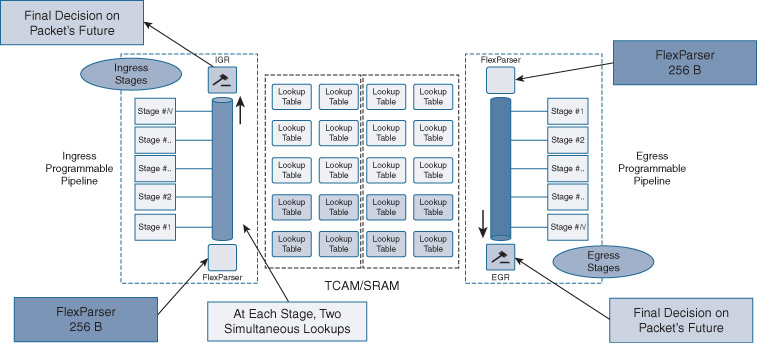
Notice the ingress and egress pipeline structure of preceding UADPs is maintained, as is the ability to perform up to two simultaneous packet lookups in each stage of the multistage processing pipeline. UADP 2.0 and 3.0 actually increase the total number of stages on the ingress pipeline to 17 (from 15 previously), and also increase the total number of egress stages to 8 (from 7 previously)—yielding a total of 25 stages of fully programmable packet processing. The 256-byte deep packet header lookup capability of preceding UADPs is still retained, leading to an excellent ability to “look deep” into passing traffic.
Figure 7-37 also shows more detail on the Ingress Global Resolution (IGR) and Egress Global Resolution (EGR) stages of packet processing. All UADP ASICs incorporate the IGR and EGR logic outlined herein—however, let’s delve a bit deeper into this now that we are examining the inner workings of the UADP 2.0 and 3.0 ASICs, in order to understand how this works.
The job of the IGR block in the UADP ASIC is to “sum up” and normalize the decisions made by each of the ingress programmable stages. For example, one stage may have said “Route the packet this way” while another stage may have said “Drop the packet due to matching a security ACL entry.” The IGR resolves all of these various decisions and provides the “final decision” as to what the packet’s fate, and further processing, will be. On the egress side of the chip, the EGR performs a similar function at the end of the egress pipeline. All UADP ASICs incorporate this IGR/EGR logic for their programmable pipelines, and Figure 7-37 shows this in more detail.
And what transistor count did all of this advanced capability on UADP 2.0 and 3.0 come with? An impressive 7.46 billion transistors on UADP 2.0, and a very impressive 19.2 billion transistors on UADP 3.0. Pretty striking for something you can hold in the palm of your hand!
Let’s now examine the key platforms that the UADP 2.0 and 3.0 ASICs support. These are the Catalyst 9000 Series switches—the Catalyst 9300, 9400, and 9500, which together form the foundation for the next era of enterprise networking.
Figure 7-38 shows the Catalyst 9300 platform, the industry’s new standard for advanced stackable access switches. The Catalyst 9300 is offered in 24-port and 48-port versions with Gigabit Ethernet front-panel ports, with both non-PoE (Power over Ethernet) and PoE-capable (PoE+/UPoE) models available. As well, a version of the Catalyst 9300 is offered with mGig-capable front-panel ports, offering connectivity of up to 1G/2.5G/5G/10G Ethernet with UPoE capability. All of the Catalyst 9300 models support modular fans, modular power supplies, and fully modular uplink capability, with 4 × 10G, 8 × 10G, and 2 × 40G uplink modules available. In addition, a new 2 × 25G uplink module is now available for the Catalyst 9300.
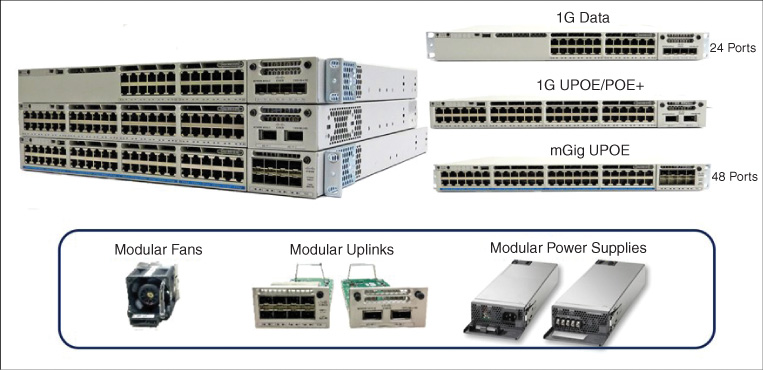
Figure 7-39 shows the Catalyst 9400 platform, the industry-leading flexible, modular access switch family. The Catalyst 9400 is the first modular switch to be based on the UADP ASIC, and is offered in sizes ranging from four-slot through seven-slot and ten-slot varieties (although the Catalyst 4500 Supervisor-8E and -9E incorporated the UADP ASIC, they used this only for ancillary functions, whereas the Catalyst 9400 family uses the UADP ASIC as its primary forwarding chipset). All Catalyst 9400 switches offer two dedicated Supervisor slots for packet switching and processing redundancy, even in the smallest four-slot switch models, ensuring the highest levels of resiliency for demanding access-layer switch applications.
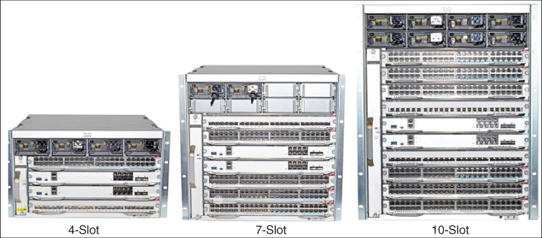
The Catalyst 9400 family offers simple, functionally transparent line cards and centralized packet processing, building on the legacy of its predecessor platform the Catalyst 4500E, while offering a whole new set of packet-processing throughput and flexibility made possible by the use of the UADP 2.0 ASIC. The Catalyst 9400 also offers key hardware innovations such as a fan tray that is removable from both the front and the back side of the switch, as well as N+1 and N+N redundant power supplies. Along with the other Catalyst 9000 switch family members, the Catalyst 9400 platform boasts an ergonomic design that eases installation and use of the platform with such functions as blue beacon capability and RFID support to allow for easy identification of system components—showing the attention to detail and serviceability that is the hallmark of the Catalyst 9000 Series switch family.
Finally, Figure 7-40 shows the Catalyst 9500 switch family. Intended as a series of fixed-configuration core and aggregation switches, the Catalyst 9500 family provides a high level of port density for 10G, 25G, 40G, and 100G Ethernet in an extremely compact and powerful form factor, while also offering resiliency across important areas such as modularity for switch elements such as fans, uplinks, and power supplies.

For many modern enterprise network designs, sophisticated and high-performance functionality in a small package is critical. The Catalyst 9500 family of switches is designed to deliver against this need. With the capability to provide high-density 10-Gbps Ethernet, 40-Gbps Ethernet and now—with the latest additions to the Catalyst 9500 family based on UADP 3.0, high-density 25-Gbps Ethernet and 100-Gbps Ethernet—in a very compact form factor, the Catalyst 9500 leads the industry in terms of functionality and performance—all with the flexibility enabled by UADP.
So What’s Common Across All of These Variants of UADP?
Flexibility is the common denominator among the UADP variants. Flexibility supports future growth in network design possibilities and provides investment protection as the network evolves, which is a critical element to support Cisco DNA. The only real constant in networking, as in life itself, is change. Cisco’s UADP-based switch platforms are designed to deliver, with this need for flexibility and investment protection in mind.
In the future, the FlexParser and programmable pipeline capabilities of Cisco’s powerful UADP ASIC make it possible to support many additional protocols and capabilities, based on market and customer demand, as indicated in Figure 7-41 (note, protocols marked with an asterisk in this figure are examples of potentially possible future capabilities, not currently committed features).
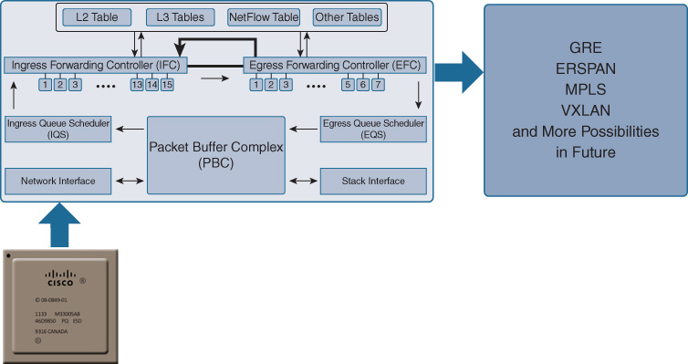
The level of flexibility provided by Cisco’s future-looking UADP ASIC is unparalleled in the industry, and is an absolutely critical underpinning for the evolution of the network with Cisco DNA.
UADP—Summing Up
Let’s sum up what we’ve discussed about UADP.
Cisco’s Unified Access Data Plane ASIC provides a level of robustness, flexibility, and capability unequaled by any networking silicon in the industry. Designed from the ground up for flexibility, and representing the intellectual capital and effort of over five years by Cisco in development, the UADP ASIC offers Cisco customers a level of investment protection that is second to none.
Cisco customers investing in platforms that leverage the UADP ASIC, as outlined in Figure 7-42, reap the benefits of the power and capability it provides today—and the flexibility that it provides to drive investment protection for the future.
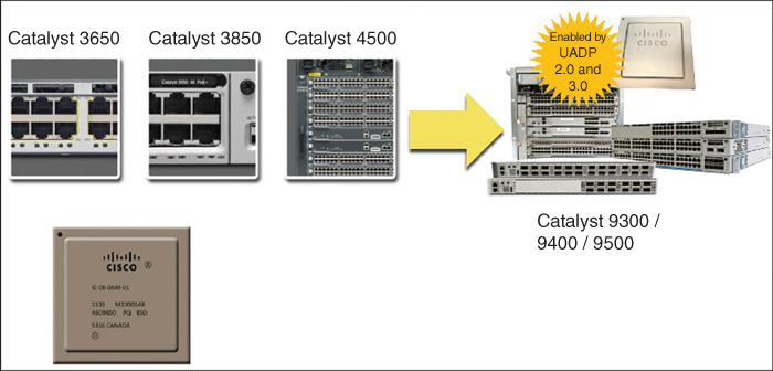
Simply put, the UADP ASIC, and the platforms it powers, allows your network to continue to evolve as networking evolves, which is a crucial consideration given the pace of change in today’s rapidly digitalizing world. Although there are always limits to any platform or chipset, UADP provides an excellent level of flexibility for network functions today and tomorrow.
The solid set of functionality provided by UADP, along with Cisco’s other flexible networking silicon, forms a strong foundation for Cisco DNA, and an excellent foundation for the future of networking.
Flexible Routing Silicon: QFP
The Cisco QuantumFlow Processor (QFP) forms the heart of the Cisco Aggregation Services Router 1000 (ASR 1000) product family. The ASR 1000 is designed to deliver on the inherent feature and scale requirements of enterprise routing as a premier WAN aggregation router, but to do so with the ability to evolve to current—and future—performance and capabilities.
WAN routers face very different scaling, performance, and feature requirements than LAN switches do. A router serving in the WAN aggregation role such as the ASR 1000 may be connecting in hundreds or even thousands of remote branch sites to a common WAN core or distribution location. In doing so, it must support key functions for all of these branches—QoS for connectivity and application prioritization, encryption for privacy and security, tunneling for use over multiple WAN carrier backbones and technologies, and more.
But with today’s ever-increasing WAN speeds, the older, more traditional WAN routing platforms such as the venerable Cisco 7200 Series—long a workhorse of the fleet as a WAN aggregation router—were outstripped several years ago. As a traditional WAN router based on a CPU architecture for forwarding, the Cisco 7200 and its brethren offered excellent flexibility. However, their purely software-based forwarding approach couldn’t scale above a few gigabits per second, which is an issue any CPU-based platform faces.
Scaling up by installing more and yet more such routers at a central site was not a sustainable solution for enterprise customers. What was needed was something that could support the three key routing attributes of performance, flexibility, and programmability, and do so at ever-increasing scale and density, as shown in Figure 7-43.

So, what’s the answer? Enter Cisco QuantumFlow Processor, a scalable and unique piece of flexible silicon designed specifically for the demanding requirements of the WAN aggregation role.
QFP—An Introduction
Cisco QFP is a powerful example of flexible silicon in action, designed for WAN routing and aggregation as shown in Figure 7-44.
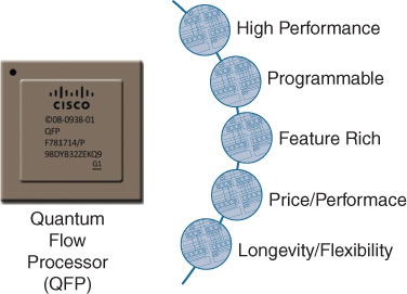
As such, QFP delivers on several of the key attributes that are needed for this role:
High performance: In the ASR 1000 platform, QFP is scalable as high as 200 Gbps with the latest Embedded Services Processor engine (ESP-200), or as low as 2.5 Gbps for more entry-level solutions—spanning a huge range of WAN throughput needs with consistent features and performance. Integrated support for encryption also scale up as high as 78 Gbps with the ESP-200.
Programmable: QFP is inherently flexible due to its multicore hardware architecture, which delivers extreme flexibility comparable to a more traditional CPU-based system, but with massively increased multidimensional scale.
Feature-rich: The ASR 1000 by its nature and position in the network must deliver on all of the most critical features for a WAN aggregation device—not just raw throughput, but also enhanced services such as NAT, encryption, ACLs, NetFlow, and more. By offering hardware assist for many of the features, QFP enables the ASR 1000 to offer not only best-in-class performance, but also unparalleled feature richness—without scale or performance compromise.
Price/performance: As a Cisco-designed piece of flexible silicon, QFP is targeted directly at offering the best price/performance ratio for the applications it is designed for, and deployed in. QFP offers the right blend of performance, features, and price that makes the platforms leveraging it, such as the ASR 1000, unique in the industry.
Longevity and flexibility: These two attributes are key design goals for the QFP architecture, and are deeply intertwined. QFP was designed from the ground up as a chip architecture that could live a long time in the marketplace and be taken through several iterations. Central to this longevity in terms of lifetime in a customer network is the flexibility that QFP offers—through a simple software upgrade, a platform leveraging QFP can deliver a whole new, enhanced set of software functionality, delivered at hardware throughput speeds. The key to this capability is the hardware architecture of QFP.
Much like the UADP ASIC examined previously in this chapter, QFP is the result of a five-year design process. However, the outcome produced a markedly different chip than UADP—different because it was designed to achieve different goals, and to be placed at a different position in the network, with widely varying requirements compared to those desired from a LAN switch.
QFP is fundamentally based on a massively multicore processing design, with hardware assists for many key networking attributes and functions. As shown in Figure 7-45, the original QFP design was based on a 40-core processor design (with initial deliverables of 5 Gbps to 10 Gbps performance), which scaled up to today’s total of 64 parallel cores and 200 Gbps of system performance.
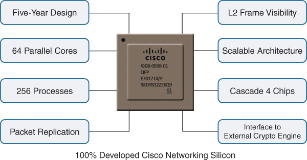
Each processing core handles up to four threads of operation, allowing for up to 256 independent processes (such as packet forwarding and replication) to take place simultaneously within QFP. In addition, multiple QFPs (up to four) can be cascaded together in a system, and an interface is provided to allow attachment of an external encryption engine (a common requirement in WAN core routing).
The CPU in your laptop, desktop, or server might have two, four, or maybe even six or eight cores. The initial QFP hosted 40 cores, and today’s QFP boasts 64 cores. Each processing core has roughly the performance of an entire Cisco 7200 router, so we are talking here about having a single chip with the power of 64 previous-generation routers, plus hardware assists for things like ACL lookups, QoS capabilities, encryption/decryption, etc., all shrunk down to a single chipset.
QFP was developed to deliver on next-generation routing needs, and its success can be judged by the wide acceptance that platforms leveraging QFP, such as the ASR 1000, have achieved in the marketplace.
QFP—Diving Deeper
Let’s take a look inside QFP and see how it delivers some of its routing magic.
Figure 7-46 shows the basic block diagram of the QFP architecture. Notice that the packet-processing array shown at the top left is the collection of 40 or 64 processing cores noted previously—each with the equivalent processing capability to an entire Cisco 7200 router, and each with access to the full range of hardware assists offered by the QFP silicon, some of which are outlined in the functional block titled “General Resources.”
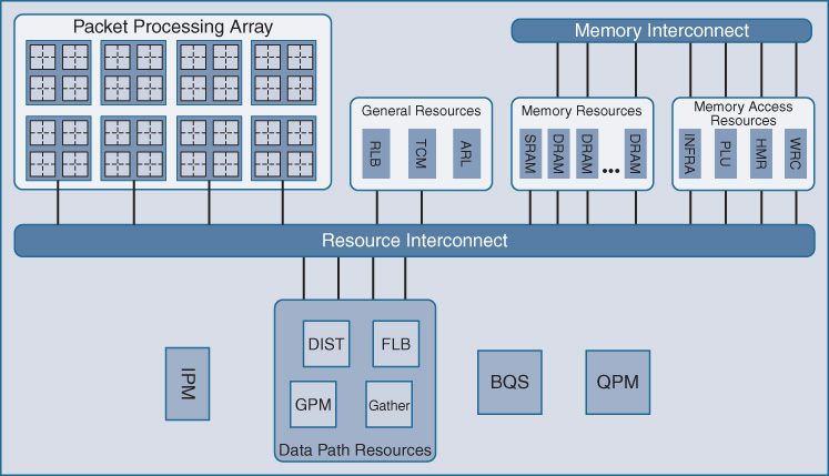
These include hardware-based TCAM for ACL lookups, routing table lookups, and packet replication. Another significant area of note is “BQS,” the buffering, queueing, and scheduling functionality of QFP, which implements its advanced and unique QoS and packet-queueing architecture. Let’s examine several of these key functional blocks.
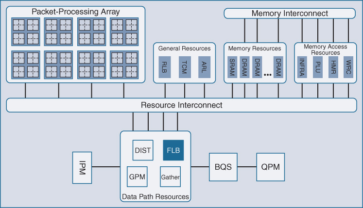
First, it is important to understand how QFP handles traffic load balancing across its array of processing cores. This is highlighted as FLB in Figure 7-47.
It is necessary to ensure that as traffic is crossing a multicore processing array, such as that employed by QFP, that packets stay in order. Out-of-order packet delivery and packet reordering are typically pathological processes in a network, as TCP at the receiving node elsewhere in the network may sense out-of-order packet delivery as a sign that congestion exists in the network, and could trigger unnecessary delays or retransmissions that could slow down end-user data access and congest network pipes.
The designers of QFP were well aware of this possible issue. However, performing the trade-off of doing flow-based traffic load balancing across processing cores, such that any particular flow only used one processing core to ensure in-order packet delivery for that flow, would limit the performance of any one flow to the performance of a single processing core. This is an unacceptable outcome for high-performance network flows where the ability to harness the full throughput of QFP-based platforms is desired.
The job of the Flow Load Balancing (FLB) component within the QFP silicon is to assign each incoming packet to a free packet-processing element (PPE) within QFP’s packet-processing array. Packets are “sprayed” across the array, leveraging the full throughput of the QFP design. Packets exiting the array are always reordered into their appropriate sequence, preventing out-of-order packet delivery. QFP does not reorder incoming packets, yet allows dozens of packets to be processed in parallel, including packets which may need more processing (NAT, etc.) than others do. The hardware-based lock capability within QFP ensures that traffic is handled and delivered optimally, and with consistent high performance.
Figure 7-48 highlights the packet-processing array.
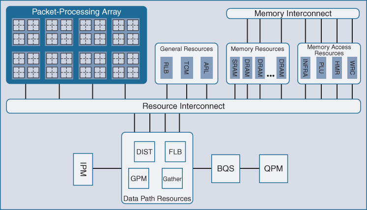
QFP’s packet-processing array is in many ways the “heart” of QFP, and the site where QFP’s flexibility becomes manifest. This is because all of QFP’s packet processors are just that—they operate as packet-processing engines, reprogrammable through software to deliver on the functions configured in the WAN routers they support. This is the key to delivering the flexibility demanded by WAN routing, married to the ever-increasing need for speeds and feeds that WAN aggregation routing is subject to.
Each packet processor within the QFP processing array can process up to four threads of operation in hardware (and because this is solely within the data plane of operation of the device, this equates to up to four packets in flight across any individual PPE at one time—or up to 4 × 64 = 256 packets in flight across a 64-core QFP at once). The operation of each PPE ensures that if a given thread is waiting for a particular function (such as a hardware lookup, for example), the other three threads operating on that PPE can continue to be processed unabated, ensuring consistent and optimal traffic handling.
In general, most functions can be handled in a single pass through the PPE, but in the event that recirculation is required (for example, with multicast), QFP handles this in a speedy and efficient fashion—ensuing that recirculated high-priority traffic continues to receive its appropriate level of treatment even when newer, incoming but lower-priority traffic may have arrived in the interim.
The PPEs themselves operate at a speedy 1.2 GHz and have access to a wide array of hardware-based assists. For example, ACL lookups are a common core WAN routing function. QFP does such lookups in TCAM for rapid resolution, as highlighted in Figure 7-49. Likewise, lookups such as Weighted Random Early Detection (WRED) for QoS, flow locks, and the like are all handled in hardware, offloading these functions from the PPE processors and leading much better performance as well as more consistent sustained throughput.
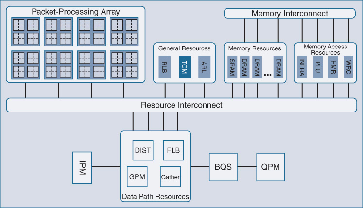
With the ability to perform hundreds of millions of searches per second, QFP offers performance that is well matched to the needs of WAN aggregation routing, where packet rates reach extremely high values, and consistent high performance is needed. Layer 1 cache for each PPE individually and Layer 2 cache shared across all PPEs help to ensure that packet processing is always optimized. As a general rule, if many of the incoming packets all require the same or similar data-plane processing, as is often the case in many WAN routing scenarios, the cache and memory architecture of QFP ensures the speediest and most optimal handling for the traffic involved.
BQS, the buffering, queueing, and scheduling component within the QFP architecture, is highlighted in Figure 7-50.
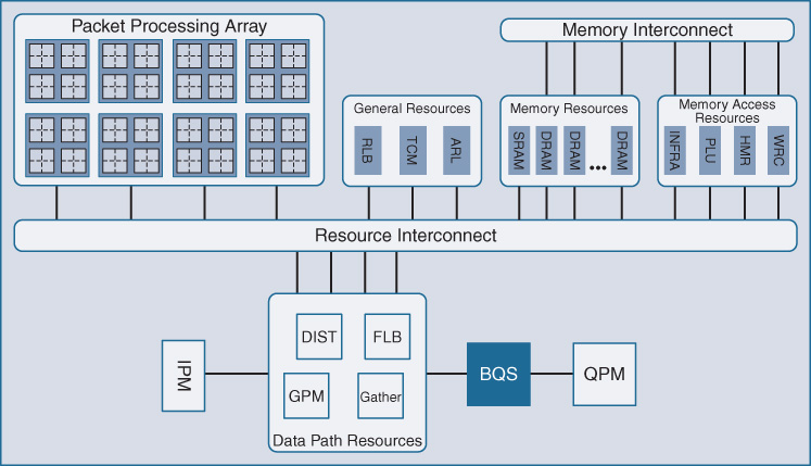
QoS is a difficult task for any WAN router. Traffic must be recognized for what it is—various applications streams must be classified and sorted out one from another—and then traffic must be appropriately marked via Differentiated Services Code Point (DSCP) per the configured policies on the router, and queued appropriately out to the set of destinations involved. Of course, some applications are more important than others—again, per configuration by the network administrator—and bandwidth is always a constrained resource, so some applications must be given preferential access over others, with the use of multiple queues (priority and nonpriority), traffic policers, traffic shapers, etc.
Now, think about the job that a WAN aggregation router has to do. It not only has to do this for one set of queues and traffic flows the way a branch router would, but has to do this in a head-end WAN routing role for literally hundreds or even thousands of downstream routers, which could be configured with multiple different bandwidths, multiple different policies, and widely varying anticipated traffic flows and application types.
Handling this daunting challenge within QFP is the job of the BQS portion of the silicon. BQS implements up to 128,000 queues in hardware (depending on the QFP version in use). QFP also offers up to five levels of queueing hierarchy for the richest set of QoS functions available on a midrange WAN aggregation router, providing flexible allocation of scheduling resources.
In a more traditional CPU-bound router, many of these QoS tasks would be very taxing for a processing core to accomplish. QFP does not expend any cycles within the PPE array to process such capabilities—the BQS portion of the QFP’s flexible silicon performs all of these tasks, offloading the PPE cores for other tasks and ensuring consistent high performance for QoS-processed traffic flows.
QFP—Use in Platforms
QFP is used as the data plane for the Cisco ASR 1000 Series WAN aggregation routing platforms. These platforms now span a wide range of physical sizes and interface densities, as outlined in Figure 7-51.
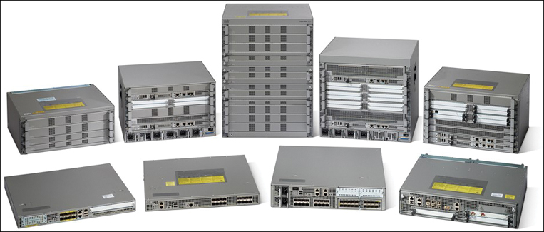
Offering scalability up to 8000 VRFs, 4 million IPv4 routes, 4 million IPv6 routes, 8000 IPsec tunnels, and 200 Gbps of throughput at the top of the product range, the ASR 1000 Series offers a set of WAN routing platforms to fill almost any need.
By separating the control plane functions of the router from data plane processing offered by QFP, and offering redundancy for both control plane and data plane functions within selected ASR 1000 models, the ASR 1000 Series platforms are custom-tailored to provide the right “fit” for many different places within the network, and for many different customer and traffic profiles.
UADP and QFP—Summing Up
UADP is a piece of Cisco flexible silicon, optimized for the growing and changing needs of the LAN switching role. QFP is a piece of Cisco flexible silicon optimized for the very demanding needs of the WAN aggregation routing role. The actual internal architecture of QFP is quite different from UADP, which was examined previously. Both sets of requirements, as well as the placement within the network, for platforms using QFP and UADP are quite different.
However, both chips have many similarities as well.
Observe that several important operational aspects are preserved across both UADP and QFP. The most important of these is flexibility. Both UADP and QFP offer silicon platforms that are inherently flexible and programmable, a vital attribute as Cisco DNA—especially as the capabilities that Cisco DNA must support continue to evolve over time. As shown in Figure 7-52, as new protocols, new functions, and new packet header formats and encapsulations come along, high-performance network hardware needs to be able to handle these without performance or traffic-handling issues.
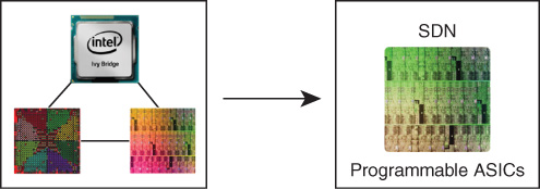
UADP and QFP were designed from the ground up for this kind of flexibility—exactly the type of flexibility required in networks today, and tomorrow. It is a testament to Cisco’s Engineering teams and their foresight that they saw these types of requirements for flexibility coupled with high performance coming years ago, and designed UADP and QFP to meet these needs, thus laying the solid hardware foundation for Cisco DNA.
Wireless: Providing Innovation for Mobility
Having examined the hardware innovations that Cisco is driving in the switching and routing areas with UADP and QFP, respectively, it is also important to note the hardware innovations that Cisco is providing in the area of wireless mobility. This is vital because wireless—and more specifically, 802.11 wireless—is now the primary “on-ramp” into the enterprise network in many organizations today.
While Cisco is driving many areas of innovation with respect to wireless, the following are a few critical ones to highlight in terms of flexible hardware:
Integrated antenna arrays in Cisco Access Points (AP) to enable Cisco Hyperlocation, allowing for advanced location-tracking capabilities for associated wireless devices
Advanced beam-forming technology in APs to maximize radio throughput for clients
Flexible Radio Assignment (FRA) capability in APs to enable customized and optimized radio coverage
Advanced packet capture capability (Intelligent Capture) in APs to enable sophisticated network analysis and troubleshooting
These capabilities, and more, are instantiated in Cisco’s latest generation of APs, the Aironet 4800 Series, as illustrated in Figure 7-53.

The Aironet 4800 provide many advanced capabilities that allow network managers to optimize the available radio spectrum and RF environment in their wireless deployments, allowing the delivery of the best possible wireless network infrastructure, and wireless deployment, for their organization.
To see why this is the case, let’s examine two key areas of innovation in the Aironet 4800 wireless platform: Flexible Radio Assignment and Intelligent Capture.
Flexible Radio Assignment
Flexible Radio Assignment (FRA) enables the Aironet 4800 to be designed and deployed with a macro-cell/micro-cell architecture, if so desired by the network manager. Normally, the multiple radios in the Aironet 4800 are deployed with one radio handling the 2.4-GHz band, and another handling the 5-GHz band. While functional, this does not necessarily lead to the optimum coverage for a given area and set of clients. Today, many clients support the 5-GHz spectrum, and this wireless band tends to be less “polluted” with interferers (other non-802.11 devices) than the 2.4-GHz band. The 5-GHz band also offers many more non-overlapping radio channels as opposed to the 2.4-GHz band, due to its use of higher frequency transmission.
The nature of 802.11 wireless communications is such that each wireless channel (and the clients using it) operates as a shared medium, so that when one user is transmitting, others have to defer and wait for the channel to become free (with Multi-In, Multi-Out [MIMO] techniques, this is improved somewhat, but the basic principle remains). The radio link speed at which any given client associated to a particular AP is affected (among other factors) by its distance from the AP’s radio—all things being equal, the farther away the client is from the AP, the fainter the radio signal is, and thus the lower the data rate the client will associate to that AP at.
With many clients associated to the same AP, and using a shared radio medium for transmission, it can readily be seen that the performance (that is, the actual throughput) of a higher-speed (closer-in) wireless client can be affected by the presence of lower-speed (farther-away) clients on the same radio, and on the same channel.
As a result, you might want to optimize your deployment by choosing to have two radios in the AP operating in the 5-GHz band: one operating on one 5-GHz wireless channel with a lower power setting, and the other radio operating on a second 5-GHz (non-overlapping) channel with a higher power setting. This is illustrated in Figure 7-54.
This is exactly what Flexible Radio Assignment (FRA) with the Aironet 4800 can accommodate. By allowing the individual radios within the Aironet 4800 to be reprogrammed to operate in either the 2.4-GHz band or 5-GHz band, a macro-cell/micro-cell architecture such as that shown in Figure 7-54 can be instantiated.
This consists of having both flexible radios operate in the 5-GHz band, one with a lower power setting (and thus associating only closer-in clients, typically at a higher data rate), and the other with a higher power setting (and thus offering longer reach, but potentially associating farther-away clients at a lower data rate). By combining this with other adjacent APs that continue to offer service in the 2.4-GHz band for devices that are not 5-GHz capable, an optimized wireless deployment can be arrived at that offers holistic coverage for all clients, with optimized and seamless performance. Closer-in clients get faster throughput, and farther-away clients get maximized wireless coverage.
Key to the ability to provide advanced capabilities such as FRA is the use of software-programmable radio hardware in platforms such as the Aironet 4800. By including hardware that allows the radios within the platform to be reprovisioned between bands, and with the ability to provide flexible power and channel assignment, Cisco is able to offer a unique solution that allows organizations large and small to optimize their wireless deployments and maximize throughput for their users—all in a seamless fashion.
Given the ever-increasing importance of wireless in enterprise network deployments, the use of flexible radios in platforms such as the Cisco Aironet 4800 is critical, and provides yet another proof point as to why flexible hardware is so important in modern network implementations.
Intelligent Capture
A second area of network innovation worth noting in the Aironet 4800 is Intelligent Capture. This unique and powerful capability allows for full packet capture and analysis of user traffic traversing the Aironet 4800—even when the user or device involved may be roaming from AP to AP within the network infrastructure.
Intelligent Capture leverages the multiple radios within the Aironet 4800 platform to be able to “listen while talking” over the radio bands involved. By leveraging the powerful and flexible hardware in this wireless platform, Intelligent Capture allows for the network operator to capture a designated subset of user traffic—for example, the traffic from a user who called into the Help Desk with a problem—and pull that traffic (including full packet copies) back to the Cisco DNA Center platform for analysis, without impacting other users on the same AP.
By then providing advanced analytics for the traffic involved, common issues (such as those associated with device attachment, logon, or access) are readily diagnosed, and suggested remediation actions are presented to the network operator—all in near real time.
Intelligent Capture is an excellent example of leveraging the power of the flexible hardware provided by the Aironet 4800 platform with its multiple radios, combined with the centralized and intuitive analytics provided by Cisco DNA Center, to assist in solving real-world network issues that arise in wireless network deployments.
Only with providing the fusion of advanced, custom-designed hardware functionality with software flexibility can such results be achieved. Cisco, in being able to provide the entire hardware and software “stack” in the network—including advanced analytics with Cisco DNA Center—is uniquely positioned to deliver on this important need.
It is important to note, however, that Intelligent Capture is not possible without the advanced and flexible hardware that Cisco enables in advanced wireless platforms such as the Aironet 4800—another example of why hardware continues to be so important, even in our software-defined age.
Summary
So, what does flexible hardware truly deliver? Why is it fundamentally important for Cisco Digital Network Architecture, and for your evolving network?
The two key attributes that Cisco’s programmable network hardware delivers are flexibility and investment protection. Flexibility to handle new capabilities. New protocols. New functions. And the things that haven’t been invented yet. Flexible silicon provides the opportunity to adapt to these changes, embrace them, and use them to further your business and organizational goals by evolving your network to the next level—thus providing the investment protection today’s businesses need in order to adapt to rapid change.
This chapter examined
How ASICs are designed and built
Why flexible ASICs are key to the evolution of networking
The inner workings of two of Cisco’s key elements of flexible silicon
UADP—Unified Access Data Plane
QFP—QuantumFlow Processor
How UADP and QFP provide flexibility and investment protection, allowing a smooth migration to present and future network technologies
How Cisco is enabling advanced functionality for wireless deployments in the Aironet 4800 platform, using Flexible Radio Assignment and Intelligent Capture with Cisco DNA Center analytics
And why are ASICs themselves important? Why spend so much time to understand them, appreciate them, and realize how they impact your business?
As outlined in Figure 7-55, ASICs are the fundamental foundation upon which products are built. Those products form the basis for the network solutions that you can build out of them. And those solutions are the basis for the benefits that you deliver to your organization every day, through the enterprise networks that you design, build, and manage.

With Cisco DNA, the power of flexible silicon allows your business to adapt and thrive in changing times. That is why so much time and focus was spent on the flexible silicon underpinnings of Cisco DNA.
Now, onward and upward as we begin to examine the Cisco flexible software offerings in the next chapter.
Further Reading
Harrel, Scott. “New Frontiers: Anti-Aging Treatment for Your Network.” Cisco Blog. June 19, 2017. https://blogs.cisco.com/enterprise/new-frontiers-anti-aging-treatment-for-your-network.
Sayle, B., et al. Cisco Catalyst 9000: A New Era of Intent-based Networking. Cisco Systems eBook. https://www.cisco.com/c/dam/en/us/products/collateral/switches/nb-06-cat9k-ebook-cte-en.pdf
Cisco Systems. “Cisco QuantumFlow Processor: Cisco’s Next Generation Network Processor Solution Overview.” Updated Jan. 1, 2014. https://www.cisco.com/c/en/us/products/collateral/routers/asr-1000-series-aggregation-services-routers/solution_overview_c22-448936.html.
Cisco Systems. Cisco Enterprise Wireless: Intuitive Wi-Fi Starts Here. https://www.cisco.com/c/dam/en/us/products/collateral/wireless/nb-06-wireless-wifi-starts-here-ebook-cte-en.pdf