8
Micro-relay Based Technology
The previous chapter demonstrated the limits of CMOS technology in adiabatic-type architectures. Will there be other technologies to bridge the gap? First of all, we want to exclude field-effect transistors (FinFET, FDSOI transistor, nano-wire or nanotube-based transistors, III–V-based transistors, graphene-based transistors, etc.). All of these devices have a sub-threshold conduction and certain restrictions in terms of dissipation. The tunnel-effect transistor conduction mechanism is quite different from a field-effect transistor. However, the experiments are not convincing enough for this component to be considered a possible successor to field-effect transistors. Devices that make use of the electron spins have not yet attained a degree of maturity that could guarantee them a certain future in logic applications.
So, in this book, we have chosen to focus on nano-relay technologies, which generally have extremely weak leakage currents. These devices have not yet been developed to the same scale as advanced transistors. The devices that have been created are larger in size but do however afford this technology to be considered a possible alternative. The technology is still encountering various problems due to contact reliability. In this chapter, emphasis will be put on how these devices are modeled and the perspectives of their use in very weak-consumption circuits. We will not delve into the technological aspects, as they have already been dealt with in various publications.
8.1. The physics of micro-relays
8.1.1. Different computing technologies
Using relays to perform logical functions is a very old idea and, in fact, the first ever computers were made in this way in the 1930s. The relay is actually the perfect device for Boolean applications because it has two perfectly differentiable states: an active state with a potentially high current if the generator allows it, and an inactive state in which the current is almost at absolute zero because it is limited by the surface leakage currents. The first computers were based on electro-mechanical technologies.
In 1833, Charles Babbage fascinated by the Jacquard loom, designed a mechanical computing machine, which was very sophisticated and which he called “the difference engine”. This machine could resolve equations and execute the most complicated operations in mathematical analysis. It was a programmable mechanical steam-powered computer that used perforated cards for the data and instructions. Just as with the previous versions, this analytical machine has not stopped evolving. Charles Babbage’s collaborator was the mathematician Ada Lovelace, countess and daughter of the British poet, Lord Byron. She designed a series of programs (sets of perforated cards) intended to be used in this machine. She also showed that the machine could resolve algebraic equations and manipulate complex numbers.
In 1938, Konrad Zuse began constructing the first Z series, electromechanical computers containing a memory and affording limited programing. Zuse was supported by the Wehrmacht, who used these systems for guided missiles. Konrad Zuse devised the Z1, which never properly worked due to a lack of development. In 1941, Konrad Zuse constructed the Z3. It was based on 2,600 telephone relays, read programs on magnetic tapes and worked perfectly, which made it the first functioning programmable computer. He used binary arithmetic and floating point numbers. The Z3 could record 64 numbers made up of 22 bits, had a frequency of 5.33 Hz and could perform four additions per second, or 15 multiplications in 1 min. This was the first ever realization of complex relay-based logic.
Then, vacuum tube-based technology brought about ENIAC, which is often incorrectly considered the first computer. Semiconductor-based technology then drove relays to the success that we know they enjoy today. Relay-based logic has not completely disappeared, however, as many power systems still use it when passing very high currents or very significant voltages.
In 2011, a team at Berkeley published an article proving the feasibility of an integrated circuit based on electromechanical micro-relay technology [KAM 11]. The dimensions are still significant (a surface of 400 µm2) and the functioning voltage is very high (in the scale of 10 V), but the foundation has been laid. The micro-relays are electrostatic and the distance between the mobile and fixed structures is typically 200 nm. For around a decade, research continued in laboratories in the Americas, Asia and some in Europe. When the size of the devices reduced, there were numerous difficulties regarding the transistor size. It seems difficult to guarantee its reliability. Financing agencies progressively turned their backs on this subject and a relay has not yet been undertaken by micro-electronics manufacturers. The technology, therefore, has not progressed at a sufficient speed to provide a short- or long-term solution.
8.1.2. Different actuation technologies
Electro-mechanical relays are all based on the movement of a mobile structure, which can put two conductors into electrical contact, after having travelled. There are multiple ways in which this movement can be created: magnetic force, thermal effect, piezoelectric effect and, finally, electrostatic force. It is quite difficult to make a global comparison of all these effects, but it needs to be admitted that the electrostatic effect is the most commonly used. It is actually quite simple to implement and does not require particular materials to be developed.
8.1.2.1. Magnetic relay
In 2001, researchers in Arizona proposed a cantilever that could be deformed into NiFe and was sensitive to a coil field. They were able to obtain an actuation voltage 5 V and a switching energy of 100 µJ on a surface of 20 mm2. A few magnetic relays have been created in a smaller size, but slow movement and high switching energy are the main obstacles for use in electronic logic.
8.1.2.2. Thermal relay
A thermal relay generally has four ports: two for providing thermal power and two for switching function. Materials expand under the effect of temperature in this structure. The fact that this technique is reserved for particular applications can be explained by its dissipated energy and the relatively slow physical effect.
8.1.2.3. Piezoelectric relay
This technique is based on the deforming of certain materials when an electric field is applied. It is mainly studied for electronic applications and often compared with electrostatic actuation. Some researchers consider this technique to be the most effective. Piezoelectric materials have mainly been studied for important applications: print heads, resonators, IR imaging and memories. PZT material is most commonly employed, but A1N and ZnO can also be used. Pre-polarization techniques reduce the actuation voltage.
8.1.2.4. Electrostatic relay
This is the most studied technique. We will detail it from the perspective of electronic logic. The principle is simple: in a capacitor made up of two conducting plates, the electric field is sufficient to move an electrode if it is mobile or deformable enough. Note that the force is always attractive because the charges are opposite signs. Figure 8.1 depicts a device designed by the University of California, Berkeley, made up of a mobile membrane held in place with four four-edged springs.
When a voltage is applied to the central part of the device, the attractive force moves the membrane toward the fixed electrode. The two stops at each end restrict the membrane that otherwise could become stuck on the fixed electrode. The electrical contact is then established between the two external electrodes called the source and the drain, in reference to CMOS technology. Note that the two distances, g and gd, are the actuation gap and the contact gap, respectively. When the voltage returns to zero, the springs play their role and the membrane returns to its initial position.
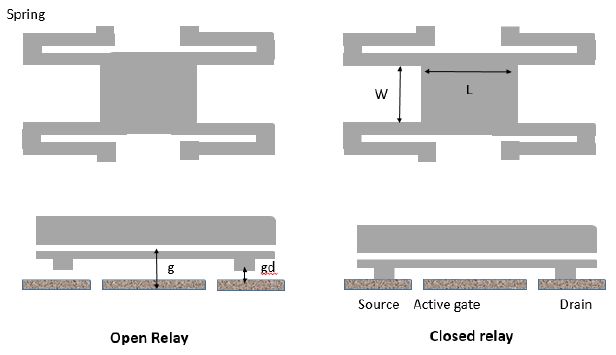
Figure 8.1. Micro-relay with a suspended membrane (according to [KAM 11])
There are other possible technologies. The membrane can be replaced by a mobile cantilever whose restoring function is ensured by the beamer’s own elasticity.
When the restoring force is not enough to overcome the electric force with the relay in the closed position, the behavior type may be bistable. The relay remains in the closed position when the voltage returns to zero.
In general, the relays show an intermediate behavior. The relay opens again when the voltage has returned to a value weaker than that allowed by the closure. The diagram in Figure 8.2 depicts this behavior and gives the definition of two characteristic voltages of this type of relay: the pull-in voltage (Vpi) and the pull-out voltage (Vpo).
Hence, it does seem possible to use micro-relays in logic instead of transistors. The extremely weak level of the current when it is in the “off” state (three orders of magnitude below a transistor’s sub-threshold current) guarantees a very weak static consumption that is much less than that of CMOS technology. It remains to be verified, however, if the functioning voltage can be further reduced in future. It will also need to be ascertained that the contact time (time that the mobile structure takes to come into contact with the fixed electrode) can also be reduced, so as to become compatible with reasonable operating frequencies. Dynamic modeling is necessary to do this.
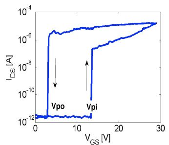
Figure 8.2. Characteristic curve of a micro-relay
8.1.3. Dynamic modeling of micro-electro-mechanical relays
This section mainly builds on the article published in 2008 by Victor Leuss and David Elata [LEU 08]. This analysis is based on a very simplified model that leads to some significant mathematical difficulties. The Hamiltonian formalism is used in this approach as it helps to easily obtain the analytical results. The physical model is the simplest model imaginable: a membrane attached to a spring and subjected to an electric force.
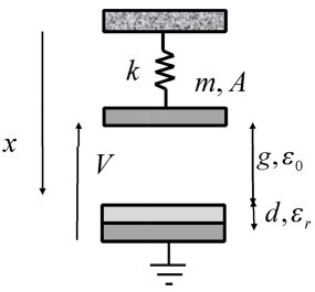
A mobile electrode of mass m and surface A is suspended by a spring with stiffness k. It is subjected to a voltage against a fixed electrode that is located at a variable distance x. An insulating layer with a thickness d and a relative dielectric constant εr sets a movement limit on the mobile electrode and confines the capacitance value. The system’s Hamiltonian function does not include the damping and is written as:

By defining the normalized variables, we obtain a simpler expression:

The movement equation is written as:

The resolution to this equation with initial conditions for the position and velocity at absolute zero is done digitally and gives the network for the curves in Figure 8.4 depending on the value of the voltage applied.
When a step voltage is applied, two very different regimes are observed. Below a value written as  , the mobile structure periodically oscillates (only the first period is shown in the diagram). Above this value, the structure travels in a non-periodic way toward the maximum value that corresponds to x = g, ignoring the dielectric thickness.
The applied voltage is expressed according to the value  of a parameter function by using an integer n, which gives a clear representation of the results.
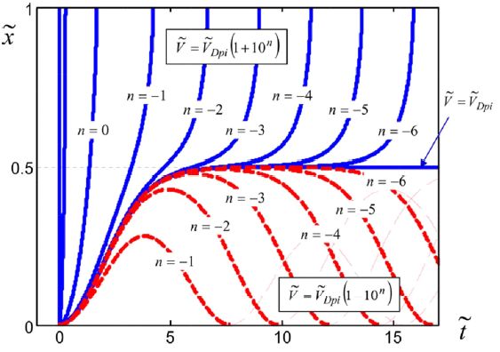
Figure 8.4. Movement of the mobile structure according to the time [LEU 08]
We can also determine a static equilibrium, defined as a state for which the total applied force is at absolute zero. The potential’s derivative is then at absolute zero, which is written as:

A third-degree equation in x is then obtained. The stability of this equilibrium can be found by studying the derivative K of the force with respect to the position,

If K is positive, the equilibrium is stable. If not, it is unstable. The limit value corresponds to K=0. If both conditions are met (the equilibrium condition and the null value of K), we obtain:


This result, unlike that in the dynamic regime, is very well known in the literature. The voltage  is called the pull-in voltage, but, in this section, we will call it the static pull-in voltage.
Now we return to the dynamic regime and we look for an expression for the size  , which is not to be confused with the static equilibrium voltage. For this voltage, the speed of the mobile electrode becomes null and so does its kinetic energy. Moreover, as the energy is conserved in a system with no such loss expected, the equality of Hamilton’s function in t equal to zero and at the time from which the velocity becomes null can be written as:

As the velocity is at absolute zero, we obtain:

From this, the movement corresponding to a null velocity can be deduced:

The maximum value for the movement is obtained when the square root is absolute zero or:


These two values are called dynamic pull-in and critical dynamic movement. The dynamic pull-in voltage is the parameter  from Figure 8.4. When distance d is ignored, we obtain the simplified formulae:

Now the two operating regimes have been explained, we need to estimate the switching time of the micro-relays. This characteristic is important in the use of micro-relays in circuits. A common idea is that micro-relays are slow devices and hence unusable for logical functions. The following analysis will allow the switching time to be quantified according to the geometric and electric parameters and to relativize this affirmation.
The energy conservation equation is the first of the calculations:

From this, the velocity value can be deduced:

When the movement is periodic, this equation can be integrated from 0 to  , with the time corresponding to the first time that the velocity has a zero value. It is also the first maximum in Figure 8.4. The position is noted as
  . The value of this time is:

The period is twice this time. An undetailed mathematical development in this section enables us to find an approximate analytical expression:

The parameter δ is defined by  and translates the difference between the applied voltage and the dynamic pull-in voltage. Remember that the real times and voltages are defined by:

Note that when close to the dynamic pull-in voltage, the parameter δ has a weak value. Its logarithm has a significantly negative value. The switching time can have a very high value.
In the non-periodic regime, the integration is made between 0 and the time corresponding to the mobile electrode’s contact with the dielectric layer, or the value  , which is approximately equal to one. In the same way, a mathematical development based on elliptic functions enables us to find the general formula for the switching time:

with,

In the same way as in the periodic regime, near the pull-in voltage, the parameter δ is very weak, the logarithm has a high negative value and the switching time can be very significant. In this case, it depends directly on the ratio k/m.
The calculation can be greatly simplified when the voltage is much higher than the dynamic pull-in voltage in the non-periodic regime:

By ignoring the parameter ζ and placing  , we obtain:

or,

All of these calculations can be used with more complex mobile structure models, particularly for including deformations. The analytical processing then becomes very complex.
An order of magnitude for the switching time can be given in the last case that is processed (applied voltage far greater than  ) by taking
  for a ½ value:

The major gap effect (parameter g) is brought to light. A switching time with an operating frequency typical of logic electronics then leads to very weak gaps, less than approximately 10 nm. In summary, an estimate about the switching time can be made in two cases:
1) If the applied voltage is slightly higher than the dynamic pull-in voltage:

2) If the applied voltage is much greater than the dynamic pull-in voltage:

8.1.4. Implementation examples and technological difficulties
Some realizations outlined below have been taken from the literature. They depict technologies and their different technical objectives.
8.1.4.1. Berkeley membrane-type Micro-relays [KAM 11]
As these have already been presented in the introduction, here we attempt to show the performances obtained at some particular points. The main characteristics are given in Table 8.1.
Table 8.1. The main characteristics of the devices
| Parameter | Average value |
| Actuation surface | 400 mm2 |
| Actuation gap | 200 nm |
| Contact gap | 90 nm |
| Contact resistance | 500 Ω |
| Grid-earth capacity | 30 fF |
| Grid-source capacity | 7 fF |
| Grid-drain capacity | 7 fF |
| Elasticity coefficient | 60 N/m |
| Mobile earth | 4,000 fg |
| Switching time | 34 µs |
| Pull-in voltage | 8 V |
These devices can perform simple logic gates, but also more complex functions (adders, memories, etc.). This pioneering work has aroused much interest and many teams have since carried out research programs on this theme.
8.1.4.2. Stanford cantilever-type micro-relays [AKA 07]
The devices move along the plane. The material is TiN, which guarantees reliability and a weak contact resistance (in the order of magnitude of 5 kΩ) at the same time. Although the actuation voltage remains high (in the order of magnitude of 20 V), the dimensions are still greater than a micron. A device is shown in Figure 8.5.
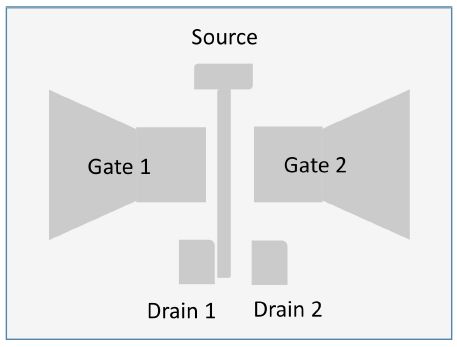
Figure 8.5. A device in the plane
8.1.4.3. The KAIST nano-relay [LEE 13]
In 2013, some Korean researchers published in Nature the feasibility of nano-relay performances switching at around 0.5 V. The name nano-relay is justified as the gap is a few nanometers. Beyond the technical masterstroke, this work is very interesting because it proves the feasibility of a low-voltage technology. This is indispensable in the field of very low consumption. The switching times are a few tens of nanoseconds. The technology chosen, however, means that it cannot be considered for large-scale manufacturing.
8.1.4.4. The works of Case Western University
This university has conducted many research projects to develop a reliable technology. They used a hard material to do this: silicon carbide (SiC). The counterpart is the presence of a high contact resistance. This compromise is that which today constitutes the main question in the development of nano-relay technology. Soft materials, such as gold, allow the technology to attain a weak value for contact resistances (less than kΩ), but it is very unreliable and some thousands of cycles are enough to render the device inoperative. Harder materials such as tungsten, titanium nitride or silicon carbide make the switches much more resistant, but the contact resistances in this case are greater than 10 kΩ. Although this value is only just higher than the conduction resistance of an FET in an advanced technology, it does not necessarily inhibit logic circuits being performed. In adiabatic logic, on the other hand, such a high value would impair energy performance as this value directly interferes with the reduction factor of dissipated power. Applications in more hostile environments have also been conceived.
8.1.4.5. The works of the European project
In Europe, we have a collaboration of universities and manufacturers studying micro-relay technology. A switching time of a few volts has been achieved thanks to a very particular design. There have also been some applications proposed in adiabatic logic.

8.2. Calculation of dissipation in a micro-relay based circuit
8.2.1. Optimization of micro-relays through electrostatic actuation
The following section was inspired by the article that the Berkeley team published in 2011 on the dimensions of micro-relays [KAM 11]. It mainly deals with optimizing dissipated energy, but it also analyzes the whole set of electrical properties.
The model on which the calculations are based is the simple model of the mobile electrode that we have already used to predict the dynamic properties. It is depicted in Figure 8.7. This model is based on a particular relay structure: a mobile membrane fixed by four springs, which moves parallel to the substrate. This is a very general architecture which can easily be transposed to other devices.
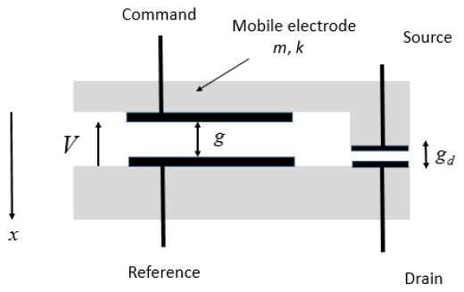
Figure 8.7. Model for optimizing nano-relays
The contact gap (gd), the interconnect capacitance (Ci), the width of the springs and the thickness of the mobile structure are assumed as given, as well as the switching energy. The contact time is then minimized. We choose the weakest possible value for the contact gap, while taking into account the technological constraints. We could develop a symmetrical approach: contact time given and minimized dissipated energy. These two approaches are actually equivalent and use the relative sensitivity method presented in Chapter 5.
When the relay is activated, the mobile structure moves from gd and the capacitance is then:

The dissipated energy will be calculated in the particular case where a micro-relay commands another micro-relay. The interconnect capacitance is fixed at the value Ci. By taking the results from Chapter 2 again, it is then possible to write the dissipated energy in the classic way:

In this relation, a is the activity rate of the logic gate in question.
The delay introduced by the relay is the most difficult to calculate. The movement time of the mobile mechanical structure is assumed to be much greater than the circuit’s electrical time constants. The results in section 8.2 allow the delay to be written in the following way:

The coefficients α, β, γ are the fitting parameters that have the following values:
- – α varies between 2 and 9 depending on the damping function (2 when the quality factor is high);
- – β varies between 0.7 and 1.4 depending on the damping function (0.7 when the quality factor is high);
- – γ varies between 0.3 and 0.4 depending on the damping function (0.4 when the quality factor is high);
- – χ is close to 0.8 and translates the delay’s damping when the applied voltage is close to the pull-in voltage.
This relation is slightly different from that obtained in the simple dynamic model:

The elasticity coefficient k of the mobile depends on the dimensions of this structure and Young’s modulus E. A beam with the length L, thickness h and width W will have a coefficient k equal to:

The method is to minimize the given value of delay with the constraint given by the dissipated energy. Another way to do it would be to define a figure of merit, for example, the product of the delay by the dissipated energy, and then to minimize this factor. In this precise case, this last method does not give any useful results, so we will choose the first that best corresponds to the real constraints: reducing the delay but maintaining a reasonable consumption level. The optimization method is a Lagrangian method written in a more general way.
In order to determine the minimum of a function F(x, y, z) under the constraint G(x, y, z) = G0, we begin by forming the Lagrangian function equal to F(x, y, z) + λ(G(x, y, z) – G0)) and we then look for the minimum of this function. Then, it can be written that:

The relative sensitivities of the functions in question with respect to all the parameters are equal. This method has also been used in Chapter 5:

This method is applied to the energy function and the delay. The variables or parameters to be determined are the supply voltage VDD, the actuation gap g, the actuation surface A and the pull-in voltage. The gap gd is assumed to be fixed by the technological constraints.
We define Vnorm by the relation:
Then, we obtain:
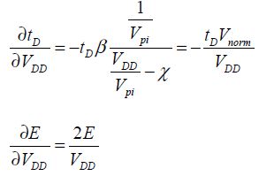
So,

By performing the same operation for g, it can be written that:
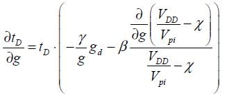
Because  , we obtain:

Similarly,

The term Cnorm is defined by:

From this, it can be deduced that:

The equality of the sensitivities relative to the supply voltage and the gap allows us to obtain an interesting relation:
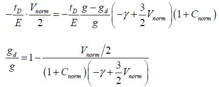
Assuming that γ is smaller than Vnorm, we obtain:

When the interconnect is negligible, the ratio is 2/3. This relation is very important in micro-relay design.
Now, we study the relative sensitivities in relation to the actuation surface, which fixes the device’s dimensions:
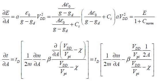
By defining mnorm by the ratio between the actuation part’s mass and the mobile structure’s total mass, the below equation can be obtained:

The equality of the relative sensitivities with respect to the gap g and the actuation surface A results in the following equation:

In order to go further, we must use the optimal gaps ratio and have an estimate of Vnorm. The quantities Cnorm and mnorm are given by geometry.
As the dissipated energy depends only on the supply voltage, the actuation surface, the gap and the interconnect’s capacitance, there is no other place to look for the relative sensitivity equations. On the other hand, it is possible to look for a minimum delay against the length L of the mobile structure. In the Berkeley model, the mobile structure is fixed by four springs and the length L is the length of these springs. When the mobile structure is a beam, it is the length of the beam itself that needs to be taken into account. By defining the spring’s sensitivity as:

we can show that the optimum is attained by:

The coefficient κ in the Berkeley model is in the scale of –0.4.
This result combined with the relation coming from the equality of the relative sensitivities against the gap and the surface allows the following relation to be written:

As the ratio between the gaps is fixed, the size Vnorm is then determined. This then enables the value Vpi to be determined.
The equality of the relative sensitivities against the actuation surface and the voltage gives the following equation:

From this, the value of Cnorm can be deduced, which enables the actuation surface A to be fixed:

As the actuation surface is determined, it is possible to fix the value of the supply voltage VDD because the energy dissipated is given and because the two gaps are also fixed. The relation between the dissipated energy and the voltage is actually written as:

The following step is to determine the pull-in voltage, which can be done by using relation [8.16] because the sizes (VDD, Vnorm) are now known:

The last step is to adjust the length of the springs according to the value of Vpi, which is now known. In theory, the relative sensitivities method allows the micro-relay parameter set to be determined. The most important result is the existence of an optimal ratio of 3/2 between the actuation gap and the contact gap.
8.2.2. Adiabatic regime solutions
The considerations presented in Chapter 7 have enabled the negative effect of the field-effect transistors’ threshold voltage to be brought into light in adiabatic architectures. Micro-relays do not have this major disadvantage because when the current is in the “off” state, it is a few orders of magnitude lower than the transistors’ sub-threshold current. At first analysis, the pull-in voltages could be considered an equivalent to threshold voltages in adiabatic architectures. A more refined analysis of the micro-relay based logic gate architectures reveals that the pull-out voltage, not the pull-in voltage, plays the same role as the threshold voltage. If we can admit that the pull-out voltage can be reduced to a weaker value without causing a major inconvenience, we can prove the usefulness of micro-relays.
In adiabatic gates, the resistance value of the switch in the active state directly contributes to the energy performance. It needs to have values lower than a few kΩ, when significant gains are contemplated. This point is an important safety bolt in using micro-relays. It actually seems very difficult to obtain a strong functioning endurance (measured by a number of logical changes before defects appear) and a fairly weak contact resistance at the same time. Soft materials (gold, aluminum, silver) can obtain contact resistances of below a few kΩ but the endurance is very poor. Hard materials (titanium, tungsten, silicon carbide, etc.) are capable of obtaining high reliability but the contact resistances obtained are mostly greater than a few kΩ. In this compromise lies the major difficulty.
Adiabatic gate architectures are based on the main diagram given in Chapter 2. “Bennet clocking”-type solutions have not been retained here as they are limited to very low frequencies. Pipeline-type solutions have been contemplated. The reversible pipeline is possible, but the overhead in terms of the amount of switches remains a major drawback. Very few developments illustrating this new path have been published in the literature. In this book, we have chosen to focus on the gate architectures inspired by quasi-adiabatic pipeline-type designs, which were described in Chapter 7. The works that have been identified so far are simulation works carried out by the European project NEMIAC and CEA-LETI in Grenoble. The general functioning principle of an adiabatic gate in a pipeline is depicted in Figure 8.8.
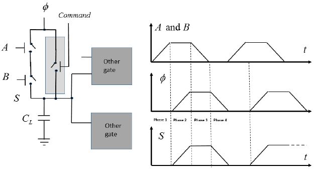
Figure 8.8. Micro-relay based adiabatic gate
The function is ensured by the relays A and B put into a series (an AND function in the example). The output is maintained and is returned to zero by the supplementary switch shown in gray. There are many ways in which this relay can be commanded: either by an external logic element (the complementary gate in a dual-rail logic, for example) or by a signal coming from the following gates in the pipeline (in the case of a reversible pipeline) or even by the output signal of the gate itself. This last mode is the simplest and will be detailed in this section. The schema shown in Figure 8.9 is then obtained.
The functioning is elementary. When the voltages at the input exceed the pull-in voltage, the A and B relays close. The supply voltage can then be adiabatically transmitted to the output. When the output voltage exceeds the pull-in voltage (Vpi), the relay T closes and stays closed as long as the command voltage is greater than the pull-out voltage (Vpo). The supply falling ramp voltage is transmitted to output as long as it is greater than the voltage VPO. Then, the output node is insulated and the output voltage stays at the pull-out voltage, awaiting the next event. In this case, there is no supplementary non-adiabatic dissipation. This is not the case in the second example where the OR function is performed and which is shown in Figure 8.10.
The behavior of this circuit is different. The output capacitor’s charge is identical to that of the previous circuit when one of the inputs is in the “on” state. The relay becomes conductive and remains that way as long as the supply voltage has not dropped to below the level of the pull-out voltage. Then, it is maintained as the output node is insulated. The behavior is different in the following event. For example, when the input moves to the “on” state, a conduction path between the output and the supply opens. The output capacitor then abruptly discharges in the supply, which creates a non-adiabatic dissipation of  . Remember that in a transistor-based gate, non-adiabatic dissipation is
  . Now, let us return to micro-relay technology.
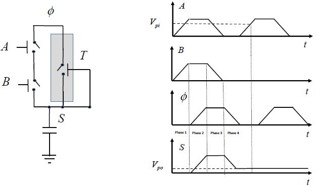
Figure 8.9. Circuit without non-adiabatic dissipation
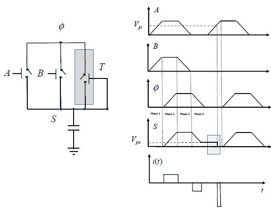
Figure 8.10. Circuit with non-adiabatic dissipation
The pull-out voltage is easily obtained by writing that, in the closed position, the restoring force is only sufficient to overcome the electric force and the adhesive force:

From this, it can be deduced that:

Therefore, it is possible to fix this voltage to any value by playing on the geometric parameters of the micro-relay and the adhesive forces. It is even possible to render it null, which introduces a new gate architecture based on a bistable-type relay.
The non-adiabatic dissipation in a bistable-based gate is then zero, but a fourth electrode needs to be introduced to move from an “on” state to an “off” state because the restoring force is insufficient. We need to account for a supplementary energy for the command of this electrode. However, as this operation can be done in each cycle, it is not necessary to provide a relay-based logic in order to perform this operation advantageously in an adiabatic way. If we call the resistance r, the resistance between the supply and the command electrode that is supposedly equivalent to a capacitance of CR, the supplementary energy to count is:

As the resistance r can be weak because it only results in the interconnect distributing this signal to the different circuit gates, the supplementary dissipation can be considered negligible. The physical restriction is the value of the adhesive energy, which cannot be recovered. The energy lost due to friction also needs to be counted if the relay is not working in vacuum.
The solution of implementing a bistable-type micro-relay, therefore, seems to be an excellent solution for years to come. One disadvantage to be aware of is that the signals are no longer symmetrical as was the case in the first structure. The reason behind this is the need to insert into the cycle a signal that has returned to zero. All of these considerations are illustrated in Figure 8.11.
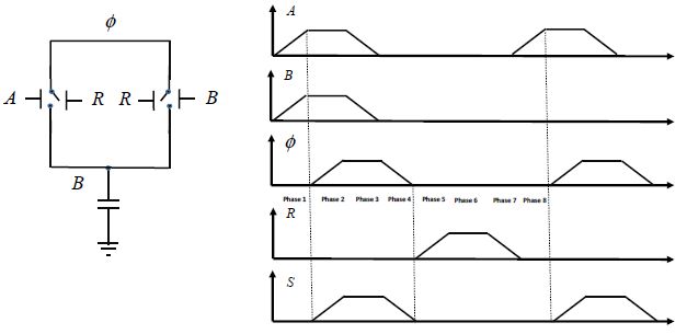
Figure 8.11. OR gate with bistable micro-relays
It is also possible to make dual-rail gates. This means that logic gates are processed by representing them with two signals, one for the logical state in question and the other for the complement. They also provide two signals, the output and the complementary output. Figure 8.12 is an example illustrating the AND function and its complement.
8.2.3. Comparison between CMOS logic and micro-relays
This last section compares the simulation performance results of the systems based either on technology involving field-effect transistors or on technology involving micro-relays. Micro-relay based technology does not yet exist on the scale of advanced CMOS transistors. Hence, a comparison based on experimental results is not possible. The energy dissipated on average per logic gate in a binary transition is the chosen figure of merit for the comparison. The logic gate is assumed to be charged by a capacitance of CL.
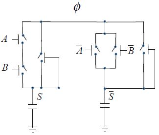
Figure 8.12. “Dual-rail” adiabatic gate
8.2.3.1. Summarizing the results obtained in classical CMOS logic
As all of the parameters have been defined in the previous chapters, they will not be defined again in this summary, with the exception of the most important ones:

Parameter y is defined based on the threshold voltage VT as:

Factor k is the ratio between the supply voltage and the threshold voltage. It is chosen according to the operating frequency. Remember that this function has a minimal threshold voltage between 200 and 300 mV. Parameter a is the gate’s activity rate.
8.2.3.2. Summarizing the results obtained in sub-threshold CMOS logic
The dissipated energy is then written as:

This function also leads to an optimal threshold voltage between 200 and 300 mV and the operating frequencies depend heavily on the choice of supply voltage, but will be less than 1 MHz.
8.2.3.3. Summarizing the results obtained for adiabatic CMOS technology in the normal regime
This result integrates the supply performances into the energy recovery using inductances. The optimal value is retained. It corresponds to a frequency of 1/4T with:


Coefficient λ expresses the ratio between the resistance of the inductance and its value. R is the transistor’s resistance in the “on” state. The energy dissipated per gate during the period is written as:

8.2.3.4. Summarizing the results obtained for adiabatic CMOS technology in the sub-threshold regime
This result also integrates the supply performances with energy recovery using inductances. The optimal value is retained. It corresponds to a frequency of 1/4T with:


The energy dissipated by gate during the period is written as:

8.2.3.5. Summarizing the results obtained for adiabatic micro-relay technology
This result integrates the supply performances with the energy recovery using inductances. By ignoring the non-adiabatic dissipation linked to the pull-out voltage or by using a bistable-type relay, we obtain:

The value R in this case is the micro-relay resistance in the active state. The optimal value of T is retained. It corresponds to a frequency of 1/4T with:

The average optimal energy dissipated by gate is then:

The average energy dissipated per gate during the period is written as:

This set of results is summarized in Figure 8.13 showing the average energy normalized, meaning divided by the term  for the different solutions depending on the operating frequency or 1/4T.
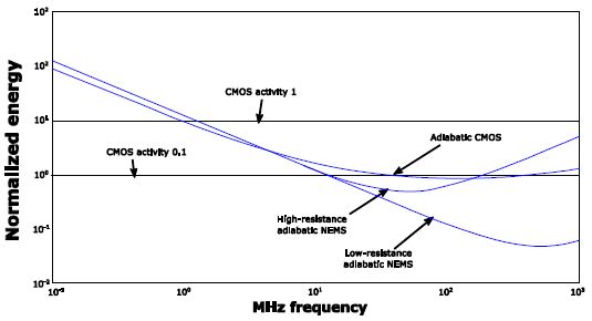
Figure 8.13. Comparison of field-effect transistor-based adiabatic solutions with micro-relay based adiabatic solutions
This curve shows the superiority of micro-relay technology if we know how to perform relays that have a weak contact resistance. The problem of the trade-off between performance and reliability remains. If technology cannot resolve this problem, the logic gate principle would need to be revisited in depth. Furthermore, micro-relays not as switches, but instead as variable capacitances, would need to be used. These very prospective research works are being undertaken by CEA-LETI in Grenoble.
