7
Quasi-adiabatic CMOS Circuits
This chapter is much more applied than the previous chapters and describes a family of circuits in CMOS technology. It also implements the adiabatic principle of charging and discharging capacitors. The industrial applications of these circuits up until now, however, remain very limited. Dissipation analysis shows that field-effect transistor-based technology limits the energy performances due to threshold voltages. Therefore, the use of adiabatic architectures is less promising than the theory would have us believe. The last chapter of this book will propose some technologies that are more suitable for implementing dissipation reduction principles. The chapter is organized as follows: a description of CMOS circuits that have implemented the adiabatic principle; a detailed estimate of dissipated energy in an adiabatic gate in both a normal regime and a sub-threshold regime; an estimate of the loss due to the particular supply that needs to be used (energy recovery supply) and, finally, a brief description of the architecture of circuits optimized for this type of functioning. This chapter draws on many ideas outlined in Philip Teichmann’s very concise book dedicated to the subject [TEI 12].
7.1. Adiabatic logic gates in CMOS
7.1.1. Implementing the principles of optimal charge and adiabatic pipeline
Let us recall the first results of Chapter 2. Dynamic consumption in a logic circuit is due to the charge and discharge of capacitors when the logical states change. Currents circulate and energy is dissipated in the form of heat in the resistive parts of the circuit. These resistive parts are not only the interconnect resistances, but also the transistor’s conduction channel resistances, when the transistors are in the “on” state. Elementary analysis based on the diagram in Figure 7.1 shows that, if the load capacitance and the supply voltage are both constant, dynamic dissipation when the states change is independent of the resistances (potentially variables). It is given by the following relation:
The supply voltage has a constant value VDD, and α and is the probability that the logic gate changes state during the time T in question.
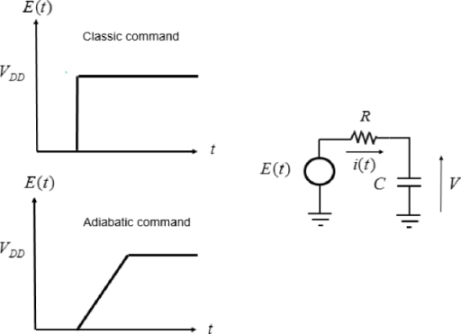
Figure 7.1. Dissipation in a logic gate
Generally, the clock period of a circuit is chosen by defining the activity rate. The average power dissipated in the gate is written as:
Note that in a logic pipeline, at the most, there is a change of state per gate located between the logic pipeline’s two registers during the period T, as shown in Figure 7.2. This basic diagram also supports many arguments and calculations put forth in the literature.
States that come from combinational logic are resynchronized by the registers at the clock frequency. The delays introduced by the gates need to be compatible with the clock period. The maximum number of gate crosses between the two registers is called the logic depth of the circuit part in question. In order for register 2 to include the combinational function result, the sum of the delays in this critical path’s different gates must be less than the operating period.
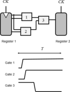
Figure 7.2. Logic pipeline
Chapter 2 helps us understand that if the supply voltage is not constant, but instead applied at a linear ramp for the duration T, then dissipation can be reduced by a significant factor, as given in the following relation:
Note that in CMOS technology, a change in logic gate’s state involves linking the supply voltage to the gate’s output, through resistance of many transistors, either in a series or in parallel. Also note that the switching time is determined by the circuit’s time constants, which are generally very weak (typically in picoseconds because the resistance is a few kΩ and the charging capacitance is in the scale of fF). The voltage application is, therefore, quasi-instantaneous. In adiabatic logic, the voltage application time is the voltage ramp rise time. It is chosen by the designer. A rise time of a few tens of nanoseconds allows for a 100-factor dissipation decrease in theory.
Implementing the adiabatic principle does, however, induce some rather large architectural constraints. Let us use the complete schematic of a logic gate, such as the NAND CMOS, and we attempt to implement the adiabatic principle by considering the supply voltage as a variable. If the input states are established with one in the “off” state (A) and another in the “on” state (B) and if both remain stable, the rising voltage according to the ramp charges the capacitor linearly and the dissipation is reduced. This operation can only be done by inspecting all of the inputs and commanding a generator, as it would be unrealistic to apply this complex command system to all of the gates. The operation of rising and descending all of the circuit’s gates voltages can only be done in an even and systematic way to the image of a common synchronization clock. This same solution is preserved in adiabatic circuits. The supply signal is called “power clock”.
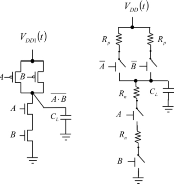
In summary, the “power clock” signal is not synchronized by the inputs, but instead, the inputs need to be synchronized by the “power clock”. If this condition were not ensured, a change of state could occur during the supply rise or fall time, which would cause a rough variation between the applied voltage and the non-adiabatic dissipation, as shown in Figure 7.4.
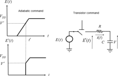
Figure 7.4. Non-adiabatic case
It is assumed that at the time t′, the logic gate’s transistor (represented by a perfect series switch with a resistance) turns on. The voltage applied to the capacity is then V′. In this case, the dissipated energy is:

The adiabatic gain is then mostly lost. The same reasoning can also be applied to the voltage’s decreasing phase. The input voltages must remain stable throughout the supply’s rise and fall phases. There are two different architectures, which allow this condition to be respected:
- – the retractable structure, also called “Bennett clocking”;
- – the adiabatic pipeline, which is the most commonly used.
These notions were outlined in Chapter 2, but it is important to study them in detail as they are the basic architectures of adiabatic circuits.
The most natural solution to the problem is that of retractable architectures. The duration of the input signal is said to be greater than that of output signals, although applying the “power clock” signal can always be done outside the input signals’ rise and fall periods. Figure 7.5 illustrates such an architecture.
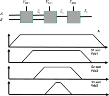
Figure 7.5. “Bennet clocking”-type architecture
Note that by the principle of this method, the output signals must have the same form as the supply signals because as the output is in the “on” state, the output is connected to the supply.
There are numerous drawbacks in this type of architecture: the complexity of the “power clock” set; the decrease in possible input operating frequency as the output frequency is fixed by the output gate’s electrical characteristics and the fact that the signal width increases at each stage as it approaches the input. Therefore, we need to contemplate another solution; the adiabatic pipeline.
The adiabatic pipeline is a pipeline-type solution, meaning that all of the operations are separated in time and performed one after the other. The only disadvantage is the increase in latency, meaning the delay between inputs and outputs. Data frequency can remain at a high value.
The reader is encouraged to carefully study Figure 7.6, which illustrates the main properties in adiabatic logic. The gray box shows a phase delay between the input signals (A,B,C) and the “power clock” signal (VDD1), which ensures the condition outlined previously. We also notice that, in this type of circuit, the logic level is not represented by the electrical level but by whether or not a signal is present. In the “off” state, there is no signal. In the logic “on” state, a trapeze-shaped signal is present.
It can also be ascertained that from stage to stage, the power clocks are delayed from a value T, the ramp rise time. At the fifth gate, the supply signal is identical to that at the first gate. Thus, generating four different “power clock” signals is sufficient. Note that, by the very principle of this pipeline, the output signals must have the same shape as the input ones. The adiabatic pipeline characteristics have been outlined, and we now need to verify whether logic gates can be designed with this constraint.
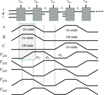
Figure 7.6. The adiabatic pipeline (example of an AND gate at the input)
7.1.2. ECRL and PFAL in CMOS
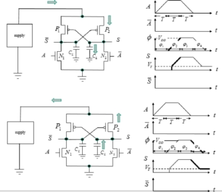
Taking the classic inverter architecture and applying it to the adiabatic principle, the signals formed are shown in Figure 7.7. The input is established in phase 1. The NMOS is then a conductor and the output is at zero. When the supply voltage rises in phase 2, the PMOS source–gate voltage remains lower than the threshold. In phase 3, the voltage A diminishes, and when the source–gate voltage becomes greater than the threshold, the PMOS becomes conductive. The output voltage then takes on the value of the supply voltage. It then sinks back down toward zero in phase 4 following the decrease in supply voltage. However, it cannot actually attain zero, as when the supply voltage is less than the threshold, the PMOS is no longer conductive. It blocks this value, while waiting for the following event.
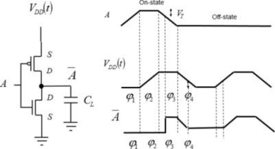
Figure 7.7. CMOS architecture’s incompatibility with the adiabatic principle
In summary, the output is very different to the signal representing the complementary input function A. The inverter function cannot be transposed into adiabatic. Different schemas need to be performed.
As shown in Figure 7.8, ECRL-type logic is a first solution to this. For the sake of simplicity, the rationale is based on the buffer/inverter, but it can be transposed to any gate. In the remainder of this chapter, the supply voltage will be written as φ(t) rather than VDD(t).
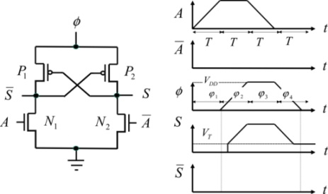
Figure 7.8. ECRL buffer/inverter
In order to fully understand how this gate functions, we must keep the following elements in mind. An NMOS transistor is conductive when the voltage between the gate and the source is greater than the threshold voltage. A PMOS transistor is conductive when the voltage between the source and the gate is greater than the absolute value of the threshold voltage (negative for a PMOS). The current provided by the supply circulates from the source toward the drain in a PMOS transistor and from the drain toward the source in an NMOS transistor.
As a first step, let us use the example of an inverter/buffer. Note that this logic processes not only the logical signals, but also the complementary signals. For this reason, it is called dual-rail logic because a state is coded by two electrical signals. Remember that the logical states are not coded by high and low voltages as in CMOS, but instead by the presence or absence of the trapezoidal signal.
Phase 1: Input establishment phase
Before signal A is applied, all voltages are at absolute zero. Signal A is then applied and turns the NMOS N1 to the conductive state. The NMOS N2 remains nonconductive because a zero voltage is applied to the gate defined by the complementary input state. The PMOS states are dictated by the output voltages that command their gates. At the beginning of the cycle, they are absolute zero, which enables P2 to be conductive when the voltage φ becomes greater than the threshold voltage VTP.
Phase 2: Evaluation phase
The signal A retains its value. The supply voltage rises. The gate’s output capacitance at the output S is then charged through the transistor P2. The P2 gate voltage is maintained at zero by the transistor N1. This NMOS is conductive because its gate voltage is higher than the threshold. Note that the output voltage jump with a value equal to the threshold voltage VTP is the cause of non-adiabatic dissipation equal to  .
.
Phase 3: Hold phase
The signal A returns to the zero value and the “power clock” voltage remains at VDD. The transistor P2 is still active because the gate remains at zero. The output then follows the supply voltage and remains at the value VDD. The transistor P1 is blocked because the voltage between the source and the gate is higher than the threshold. The complementary output is at zero potential.
Phase 4: Resetting to zero phase
The supply voltage begins linearly decreasing toward zero. The transistor P2 is conductive as long as the supply voltage is greater than the threshold. Then, it is blocked although the output node is electrically isolated, because the transistor N2 itself is also blocked, with the gate at zero potential. Then the ouput voltage remains at the potential VTP.
The output node remains isolated and conserves the value VTP. This residue would not be irritating in itself if the output returned to the “on” state in the following event as the output signal moves from VT to VDD, instead of moving from 0 to VDD. On the other hand, if the output is in the “off” state in the following event, the output quickly discharges to the ground through the transistor N2 because, in this case, the N2 gate is at VDD. The consequence is a non-adiabatic dissipation equal to  .
.
In summary, adiabatic functioning is ensured but a non-adiabatic residue that is linked to the threshold voltage appears. This residue can also be far greater than the adiabatic dissipation itself and represents a serious limitation to CMOS technology.
This architecture is simple and it uses a limited number of transistors. It can be implemented by performing any Boolean function, as shown in Figure 7.9.
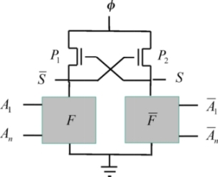
Figure 7.9. Generic ECRL gate
Positive Feedback Adiabatic Logic (PFAL) is an improvement of ECRL and its style is the most commonly retained style in operations. The improvement comes from replacing the two transistors P1 and P2 by the transmission gates, meaning PMOS sets in parallel with NMOS transistors commanded by complementary signals. The transmission resistance, meaning the ratio ΔVDS/ΔIDS in the triode-mode transistor model, is more or less constant, depending on the current, and has a fairly weak value in comparison to those NMOS and PMOS taken separately. The value reached by this resistance is written as follows, assuming that the threshold voltages are equal:

The inverter architecture is shown in Figure 7.10.
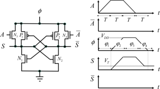
Figure 7.10. PFAL inverter
This functions in a very similar way to the previous circuit.
Phase 1: Input establishment phase
The input A is established. The complementary input is then at zero. The signal A is placed in the “on” state, which enables the N3 transistor to become conductive.
Phase 2: Evaluation phase
Contrary to the previous case, the N3 transistor is conductive from the beginning of the ramp rise as the gate-source voltage is initially VDD, which is greater than the threshold. The output follows the supply without the threshold effect. The P2, N4 and N2 transistors are initially blocked and the voltage corresponding to  is at absolute zero. The P1 transistor also becomes conductive when the supply voltage is greater than the threshold voltage.
Phase 3: Hold phase
The supply voltage is at the value of VDD throughout the duration of this phase. The same goes for the signal of the output S . The input voltage A diminishes, but the P1 transistor remains conductive throughout the duration of this phase. The N2 transistor is so conductive that the supply is greater than the threshold.
Phase 4: Resetting to zero phase
The supply voltage decreases toward zero and the output voltage follows. The P1 transistor remains so conductive that the supply is greater than the threshold. Then, the output node is electrically isolated as in the previous circuit, even though the output retains its value VTP. Depending on the input logical state for the following event, this value will be maintained or connected at electric zero, which in this case engenders a non-adiabatic dissipation of  .
.
So, both of these logic gate families bring about a non-adiabatic dissipation linked to the threshold voltages, in addition to the adiabatic consumption of  . This logic type will be called quasiadiabatic because it cannot reach optimal performance.
PFAL gates are shown in general in Figure 7.11.
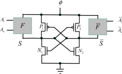
Figure 7.11. General PFAL
7.1.3. Comparison to other gate technologies
Other families are cited as an example only, because none of them are capable of eliminating non-adiabatic dissipation. Various authors have interpreted this property as a consequence of the irreversible character of the logic families considered. A method of proof by contradiction leads to this conclusion. If it were possible to conceive an irreversible circuit with a pure adiabatic consumption, meaning that it tends toward zero when the ramp rise time approaches infinity, then the dissipation could asymptomatically be at absolute zero. This goes in opposition of Landauer’s principle, which secures the minimum dissipation at ln kBT ln 2 per bit of destroyed information.
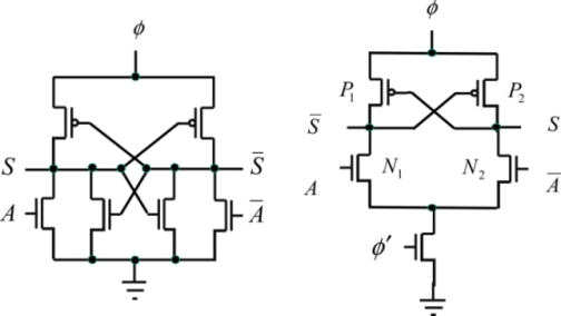
Figure 7.12. The 2N-2N2P (left) inverter and the DCPAL (right) inverter
2N-2N2P logic is a slightly more efficient variation of ECRL. The schematic is shown in Figure 7.12. DCPAL logic can also be used. A second “power clock” is needed. All of the energy performances in these circuits are rather close and the threshold voltages are responsible for the limits obtained in each case. Figure 7.13, which is taken from [BHA 11], compares the different solutions by estimating the consumption in pJ per cycle obtained by a 16-bit multiplier in 65 nm CMOS technology. There are three clock frequencies shown.
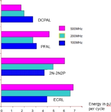
Figure 7.13. Comparison of different logic families [BHA 11]
7.2. Calculation of dissipation in an adiabatic circuit
7.2.1. Calculation in the normal regime
Dissipation is calculated using PFAL, but it can easily be transposed to other logic families.
Phase 1: Input establishment phase
All of the currents, as well as the consumption, are at absolute zero. Dissipation due to input capacitance charge is counted in the command logic gate.
Phase 2: Evaluation phase
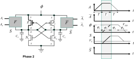
The transistors that are performing the function F are active. The transistor P1 is also active when the “power clock” signal rises as the gate is at zero potential. The N1 transistor is blocked, but there is a permanent current IN1 circulating below the threshold. The dissipated energy in both the transistor channel and the interconnect resistance, as well as the series contact, is written as shown in section 7.1:
Into this formula is integrated the resistance of an NMOS in parallel, performing the function F.
The parameters  and μ are, respectively, the channel length, the transistor width, the gate’s load capacitance, the capacitance per surface unit of the gate oxide, the ramp rise time and the mobility of the carriers. This is an estimate according to the function F, and many transistors can either be in series or in parallel. The sub-threshold current through N1 is written as:
This expression, which has been taken from Chapter 3, uses the sub-threshold current from the BSIM3 model of the transistor. The output voltage is Vs, which is equal to VDD·t/T and the voltage VGSN1 is at absolute zero in this phase. The transistor’s parameters  and φt, are the mobility, the oxide cpacitance, the width, the length, the threshold voltage, the DIBL coefficient, the ideality factor and the thermal voltage, respectively.
The energy dissipated in the N1 transistor is:

There is a fairly simple calculation, which ignores the DIBL coefficient and assumes that VDD is a lot greater than φt, and leads to the following conclusion:

The dissipation due to the current passing through the P2 transistor also needs to be counted. This is of no use to N2 because its drain-source voltage remains at absolute zero. As the source-gate voltage of P2 is at absolute zero, the energy dissipated in P2 is:

This integral is not too different to  .
.
The total energy dissipated during phase 2 is:

Phase 3: Hold phase

As the output voltage is constant, the calculation of the energy dissipated by the sub-threshold currents circulating in the N1 and P2 transistors, is:
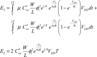
Phase 4: Resetting to zero phase
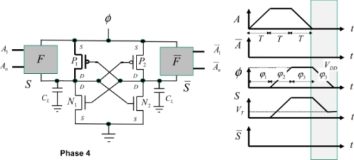
The “power clock” voltage returns toward zero. The P1 gate connected to the complementary output at zero potential ensures that this transistor is conductive so that the value of the voltage φ is greater than the threshold voltage value VT. Then, the transistor is no longer conductive and the output is electrically isolated. In reality, although the sub-threshold currents circulating in the N1 transistor are slowly discharging the output capacitance, the voltage variation is negligible during phase 3. The dissipation calculation is very similar to that in phase 1 with dynamic and static components. The only difference is that the voltage excursion is VDD – VT instead of VDD. The dissipated energy is therefore:

Phase 1: Following event
The supply voltage has returned to zero, even though all of the transistors are blocked. The transistors performing the functions F and  either become active or do not, depending on the following event’s logical state. If the function F is performed, a conduction path exists between the supply, which in this phase is at zero, and the output from the time where the implicated transistor thresholds have been exceeded. The output voltage of the value VT is then connected to the zero potential, which engenders a dissipation of
  .
.
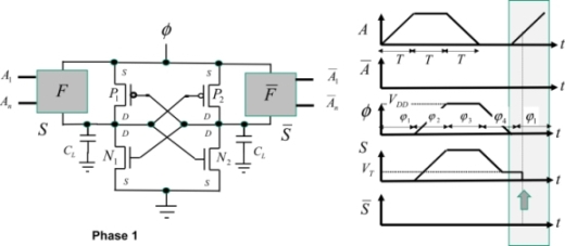
In this case, a non-adiabatic dissipation needs to be included. By contrast, the energy corresponding to the realization of the function F is counted in the energy consumed by the command gates, which are not shown in the diagram. If the function F is not performed, the output voltage is maintained and only the static consumption is to be added. Note that the non-adiabatic consumption cannot be reduced by significantly lowering the threshold voltage, as in this case the sub-threshold current would significantly increase. This point will be seen in more detail further on.
In summary, the gate’s average consumption is:
In the last term, the factor of 1/4 accounts for the fact that the probability that the function F will be performed in the following event is assumed to be 0.5. Note that, by definition of the adiabatic protocol, the gate’s activity factor is always 1. The power clock signal rises and falls throughout the cycle duration 4T for all of the input values. Some authors present this property to be like that of a “micro-pipelined” architecture with each gate also being a register.
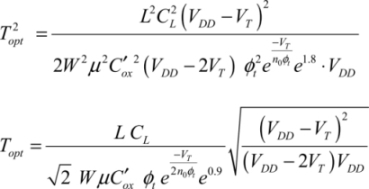
Calculating the energy optimum is particularly simple in adiabatic logic because the dissipated energy function is made up of two terms: one which varies proportionally with the ramp rise time T and the other one varying proportionally to the inverse of the rise time. The minimum is attained when these two terms are equal to that which corresponds to the optimal value of T:
From this, we can deduce the corresponding energy value:
It is now possible to optimize it with respect to VDD, which leads to:
This value is slightly different from the value 3VT in the classic case. Inclusion of the DIBL can modify the result, but in this case there is no simple analytic solution. Finally, the minimal dissipated energy can be written as:

We put:
The  function is recognized here, as it has already been brought to light in CMOS logic. The energy minimum is more evident in this case than in the non-adiabatic case because the value of the parameter m is defined (equal to 88) and is independent of the technology used. The only effect the technology has is that the coefficient n0 is modified between the values 1 and 1.5. The activity rate does not interfere because, in adiabatic logic, it is always equal to one. The optimal value of y is then 4, as shown in Figure 7.18. The optimal values obtained for n0 = 1.3 are then:

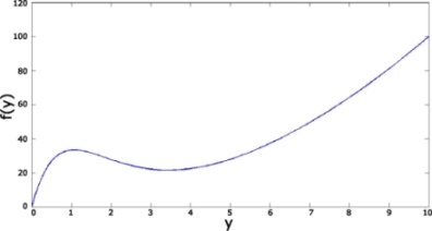
Figure 7.18. Energy optimum in adiabatic logic
Usual CMOS logic would dissipate energy of  at the voltage of 0.67 V. Therefore, there is potentially a maximum gain of 10, which is very far from the theoretical gain of the adiabatic method.
7.2.2. Calculation in sub-threshold regimes
A regime is considered sub-threshold when the supply voltage is less than the transistors’ threshold voltage. Naturally, it arises when very little is consumed. It is, however, known that the circuits are only functional when the use frequencies are very weak, practically < 1 MHz. What comes of these circuits’ performances in the adiabatic mode? This subject is little known in the literature, and thus, will be built upon in detail in this section. An ECRL-type adiabatic gate will act as a support for calculating the dissipation. The same calculation done in another family would lead to very similar results.
Phase 1: Input establishment
The currents and the dissipation are at absolute zero.
Phase 2: Evaluation
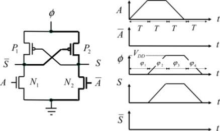
Figure 7.19. Sub-threshold adiabatic gate
The conducting components are in bold in Figure 7.19. The input voltage is assumed to have attained the value VDD. Phase 2 corresponds to the rise in the power clock’s voltage, written as φ. The P2 transistor is slightly conductive, charges the output capacitance and debits in the N2 transistor. The different currents circulating in the circuit’s transistors are written as:
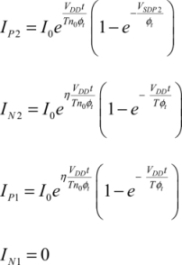
The transistors are assumed to be adjusted so as to have the same I0 current equal to:

By writing the conservation of current at the output node, the following equation is obtained:

Assuming that VSDP2 (equal to φ – VS) is much lower than φt and that the output voltage is very close to φ, we obtain:

So,

Assuming that the current passing through the N2 transistor is negligible compared with that in the capacitor, the dissipated energy in the P2 and N2 transistors is:

The dissipation in the P1 and N1 transistors is zero as the current passing through the N1 transistor is zero and the capacitance charge current is also nil as the voltage remains at zero. We put:
We can easily calculate the integral, but it has not been detailed here:

Definitively,

with
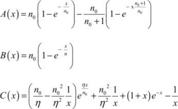
Phase 3: Hold phase
This calculation is simpler, as it is limited to dissipation in the N2 transistor, which has a significant drain-source voltage equal to VDD:

Dissipation in the P1 and N1 transistors is at zero because the current passing through it is also at absolute zero.
Phase 4: Resetting to zero phase
The supply voltage returns through the P2 transistor toward the absolute zero value. For symmetry reasons, dissipation is the same as in phase 1:

In the following phase (a new phase 1), the voltages are at absolute zero at the drain-source terminals in the transistors, and the dissipation is also at absolute zero. The gate of one of the two NMOS transistors returns to zero but the dissipated energy in this operation is not counted in the gate in question, instead it is counted in the command gate. In total, the below is obtained:
These fairly complex expressions can be simplified if we assume that x is much greater than one. k is defined by:
As in the normal regime, there is an optimal value for the rise time, a value for which the derivative with repect to T is zero:
The value of the dissipated energy is then:
For other reasons that were studied in Chapter 4, the supply voltage cannot descend lower than a few φt, which gives a value  for the minimal energy dissipated in the sub-threshold adiabatic regime. This value is very weak but the possible operating frequency is slightly weak. The subthreshold adiabatic regime cannot be considered a solution for general use.
7.3. Energy-recovery supplies and their contribution to dissipation
7.3.1. Capacitor-based supply
We are yet to deal with one major aspect of adiabatic architectures: energy-recovering supply. How these adiabatic logic supplies function is actually very specific because these supplies, on the one hand, need to deliver a trapezoid-shaped voltage and, on the other hand, they need to recover the energy stored in the logic gate’s output capacitors. In the second section dedicated to inductance-based supplies, we will see that the trapezoid-shaped signal can be replaced by a sinusoid signal without incurring a large performance loss. Now, let us return to how an adiabatic gate, such as an inverter in ECRL technology, functions.
When a logic “on” state is performed at the output in an evaluation phase (φ2 in the diagram), the gate’s output capacitor is charged through the P2 transistor. The losses correspond to the voltage variations in the transistors and interconnects. The output signal is then stable during the φ3 phase. Considering that the charge is finished then, the only losses are due to the transistors’ sub-threshold currents. In the φ4 phase, the gate’s output capacitor discharges through P2 in the supply. The current is then going in the opposite direction to that of the charging current. Note the main difference with a CMOS gate: the capacitor in the CMOS gate discharges to the ground when the output voltage returns to zero.
In an adiabatic circuit, the charging currents circulate in millions of gates connected to the four supplies that correspond to the four phases. The lines, in which the sum of the elementary currents (such as the supply’s direct output interconnect) circulate, are particularly sensitive sources of dissipation.
A natural way to achieve the necessary supply is to contemplate a storage capacitor battery with each capacitor charged to one of the trapezoid-shaped signal values. This diagram is illustrated in Figure 7.21. The gain in dissipated energy can be explained very simply. The logic gate’s output capacitor is not charged by a voltage variation equal to VDD but as a result of value variations VDD/N. Therefore, dissipation is not  , but instead:

When the number of steps is very high, we can find the gain factor to be RC/T. This calculation is proposed as an exercise.
The different gates connected to this supply are represented by a capacitance of nCL, CL being the elementary gate’s capacitance from the supply’s point of view and n being the number of connected gates. One pF is obtained for an elementary capacity of 1 fF and 1,000 gates. Note that as the gates are double, one part for the function and an other one for the complement, the capacitance felt by the supply is more or less independant of the logic activity.
The equivalent series resistance translates the effect of the transistor’s resistance and the effect of interconnect. The transistors’ resistances are a few kΩ. Those of the elementary connections are in the same order of magnitude, but they are in parallel even though the total equivalent resistance can be considered weak, such as a few ohms. This approximate representation enables us to find the order of magnitude for the system performance.

Figure 7.21. Capacitor-based energy recovery supply
Let us assume that the supply’s storage capacities (capacitances written as CT are initially charged at the voltages of VDD/N, 2VDD/N, 3VDD/N, and so on. A detailed analysis of this system reveals that these values are obtained from the initial state in which all the capacitors are discharged when a continuous voltage is applied. It can also be shown that the necessary time for attaining this equilibrium is of the order of NCT T/nCL. This relation enables us to choose the storage capacitance values.
Now that equilibrium has been attained, it is possible to command the switching transistors that are placed between the storage capacitors and the output, one after the other. The output voltage at first takes the value VDD/N and then 2VDD/N and finally VDD as the transistors are turned on. Command signals need to be applied to the gates to ensure that these transitions take place. The output voltage has the shape of a staircase, as shown in the diagram. It is fairly similar to a linear ramp when the number of N steps is high. The voltage is thus maintained at the value VDD throughout the duration T and then the inverse process is engaged. The transistors are put into conduction successively in reverse order in order to create a descending voltage ramp at the output.
At each switching step, the charge capacitance voltage moves from  , which creates a dissipation of
  in the switching transistor’s conduction resistance when we consider that the switching time constant is very fast.
In total, the energy dissipated after the N switching steps is  and twice this value, including the descent ramp in the calculation. The result does not include the switching transistors’ characteristics as the switching time is assumed to be very weak. In reality, this is not the case if the amount of N steps is significant and if the conduction resistance in the transistors is a high value. Including the resistance value Rion in the calculation, we can easily obtain the voltage value at the i switching transistors’ terminals of:

The voltage Vres is the difference between the voltage that is effectively at the output and the ideal voltage to be obtained, as shown in Figure 7.22.
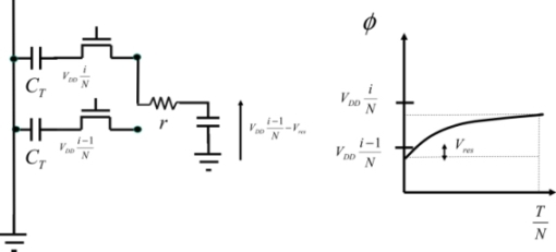
Figure 7.22. Output voltage formation
The residual voltage is obtained by writing:

or,

So it can be put that:
The dissipated energy in the i transistor’s resistance is then:

We can easily find that:

This expression is more precise than the approximation  that was used in the introduction.
Assuming that the transistors’ resistances are all equal throughout the transitions as the drain-source voltage is always close to VDD/N, the energy dissipated in a cycle is written as:
The first term is the energy dissipated in the switching transistors’ channels, the second is the dissipation corresponding to the charge and discharge of the switching transistors’ input capacitors, and the last term is the dissipation in the gates themselves. The switching transistors’ input capacitance capacity is written as Ci. Note that τ is the RionCi product equal to the product of the input capacitance by the switching transistor’s conduction resistance. This is one of the used transistor’s figures of merit. It is assumed to be constant, which is an approximation that is only valid in the transmission gate, and the hypothesis greatly simplifies the calculation. From this, we can deduce:

The total dissipation per cycle is thus:

From this, we deduce the optimal value N by the following simple derivation:
By injecting this value into the dissipated energy expression, we obtain a function of m which moves through a minimum of m, which is not very different to 2.2. This choice is called Svensson’s rule [SVE 94].
This analysis, however, is insufficient, because it is based on old transistor technologies and is incompatible with the experimental results for advanced technologies that give the optimal values to be in the order of 10. In order to make a more realistic estimate, the calculation needs to at least integrate dynamic consumption and static consumption.
Note that the transistor’s k index is the index of the switching transistor at the k step in the rising ramp. In order to render all of the transistors in the chain conductive, the gate voltage needs to be at least VDD + VT:
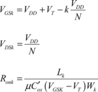
Svensson’s rule is applied when choosing the transistor dimensions. This rule decides the dimensions for the k transistor:
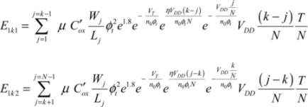
If we assume that the k transistor is conductive, the output voltage is then VDDk/N. The 1 to k-1 transistor’s drains are connected to output and the transistor’s sources are connected to the storage capacitors. When it is not conductive, the sub-threshold current circulating in the j transistor is:

The k+1 to N transistor’s drains are connected to the storage capacitors and the transistor’s sources are connected to output. The j transistor’s subthreshold is written as:

Assuming that VDSj is far greater than ϕt, the dissipated energies are:
With Svensson’s condition being applied to all the transistors, the relations become:
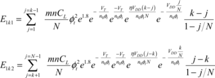
Then, we need to add up all the steps, meaning all the values of k which correspond to the signal rise:

Static dissipation during the time T in which the output conserves its constant value VDD is written as:

With Svensson’s condition being applied, we obtain:

It is easily accepted that the dissipation is equal in the rise and the fall.
In total, dissipation is calculated by including the dynamic and static terms:
In this expression, the parameter m has the optimal value 2.2. The optimal value of N can only be calculated digitally and it heavily depends on the DIBL measured by the parameter η, which significantly increases the subthreshold current. Figure 7.23 gives an example of optimization obtained by normalizing the dissipated energy per cycle by the value  .
.
Also note that applying Svensson’s conditions goes back to defining an optimal period T according to the optimal number of stages obtained and the transistor size. The optimum operating frequency obtained is quite weak (in the scale of MHz). This is the case even though the capacitor-based solution is only suitable for applications with a low functioning frequency. This is a conclusion which has been confirmed by evidence cited in the bibliography.

Figure 7.23. Optimal number of steps in a capacitor-based generator
7.3.2. Inductance-based supply
This second schema is the most commonly used. Its success can be explained by its simple implementation and its frequency performance. The performances obtained on the system level are limited by the quality factor that can be obtained in the microelectronic integration of the inductance.
Before analyzing the inductance-based supply performances in detail, let us briefly compare the differences between the possible wave shapes. The trapeze is the optimal shape for some hypotheses but a staircase approximation is a satisfying low-frequency solution, as shown in the previous section. The trapezoidal approximation by a sinusoid is also a solution. The three possible wave shapes in adiabatic logic are shown in Figure 7.24.
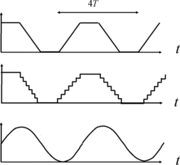
Figure 7.24. Different solutions for energy recovery supplies
Sinusoid-based solution leads to a circuit RC, with C being the total capacitive charge:
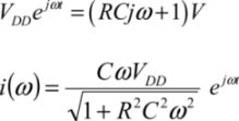
Or, by ignoring the term R2 C2 ω2 in the denominator

With the period being four times the ramping time, the dissipation in a period is:
So there is only a difference of π2/8 compared with the optimal dissipation. Remember that the N capacitor-based solution moved from  .
.
The principle of inductive supplies is to move the energy from the capacitors to the inductance by creating a resonant circuit, as shown in Figure 7.25. Another way to understand this diagram is to consider that the current passing through an inductance is quasi-constant, which enables the capacitor charge to be optimized.

Figure 7.25. Inductive energy recovery supply
The T1 transistor provides each cycle with energy in order to keep the circuit oscillating. The resistance r represents the sum of the inductance series resistance and that of the interconnect. In the first phase, the transistor is open during a fraction, aT, of the circuit’s oscillation period. This period will be written as 4T to keep the reference to the linear ramp rise time. A current circulates in the inductance and varies linearly over time because the voltage at the inductance terminals is constant. This energy is enough to excite the resonant circuit and to initiate the first oscillation cycle. The oscillation frequency depends on the inductance value and the equivalent capacitance of the load gates. By writing the oscillation period as 4T, we can write:
The energy dissipated during a cycle is the energy dissipated in the logic gates’ transistors and the resistance r. Strictly speaking, we also need to add that energy dissipated in the T1 transistor during the aT period. Outside this period, it is non-conductive. However, we will ignore this contribution in order to simplify the calculation. In total, this energy is:
The resistance R is the average resistance in a gate between the supply and the output (the conductive transistor chain’s resistance when the logical state allows it). As double gates have been implemented (one for the function and the other one for the complementary function), the average values of the load capacitance and the resistance R are independent of the logical states because when a gate is conductive, the complementary gate is not and vice versa. In other terms, the logical state changes will slightly affect the circuit’s resonance frequency.
The energy supplied to the inductance at each cycle should compensate for the energy Ed. So, we write:

The ion current at the end of the period aT is equal to:

With the oscillation condition, we can obtain:

or,
This relation fixes the time during which the energy needs to be provided to the system.
Now, let us calculate the energy dissipated in the command transistor assuming that this command is non-adiabatic:

By developing it, we obtain:

This expression can be minimized by writing that the derivatives with respect to the gate–source voltage and the transistor width are at absolute zero. So, the following is obtained:
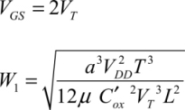
The minimal energy dissipated in the transistor T1 is then:

By injecting the inductance value L, we can write:

The total dissipated energy is therefore:

The three terms are, respectively, the energy dissipated in the losscompensation transistor, the dissipation in the logic gates, and the dissipation in the series resistance r. By calculating the first term with the usual digital values, we find that it is negligible compared with the other two.

The inductance value is then:

From this, we can deduce the optimal values of the gate voltage and the transistor width:

The dissipation in the transistor is 10-13 J, while the dissipation in the resistance r is 5.10-11 Joule. Also note that a large transistor size is necessary for maintaining oscillation.
The last part of this section is dedicated to choosing the optimal functioning frequency. A very high frequency can render an adiabatic mode less useful because the dissipation reduction factor RC/T is then reduced. On the other hand, a very weak frequency can lead to the inductance value being increased in order to conserve the oscillation condition. In this case, the inductance resistance increases and, consequently, so does the dissipation. So there is an optimum and we can estimate the value by using the following reasoning.
We assume that the inductance series resistance value is proportional to the inductance value. There is no physical reason to outline this rule, but it is verified in practice in various coil technologies and inductive devices. This rule has been proven not only in the case of coil inductances, but also for integrated micro-electronic type inductances. In practice, the proportionality coefficient is in the scale of I07. In general, we can write:

With this hypothesis, the total dissipation in an adiabatic system is written as:

The dissipation in the T1 transistor has not been included, but the non-adiabatic dissipation due to the threshold voltage has been added. By replacing the inductance with its value, we obtain:

The optimal value of T is therefore:
The minimal dissipated energy is then:
This very simple relation exemplifies the real limits of adiabatic architectures. There is still progress that can be made to limit the loss in energy recovery supplies. The limits outlined in sections 7.2.1 and 7.2.2 are the theoretical limits in both the sub-threshold and above-threshold modes relative to CMOS technology. Remember that in the normal regime, gains in the scale of 10 are possible, but no more than that, given the effects of the threshold voltage.
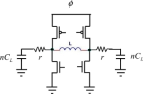
More complex schemas have been used but they are all based on the principle outlined previously. We are referring to the double generator, which enables two signals in opposite phase to be generated. Generating the second double generator is enough to ensure that there are four phases that the adiabatic circuits need. The double generator is shown in 7.26.
7.4. Adiabatic arithmetic architecture
7.4.1. Basic principles
Implementing the adiabatic principle leads to fundamental changes in the architecture of logic circuits. The supplies become generators of signals that vary in time, and the logic becomes totally dynamic with an activity rate of one. These are not the only modifications. The way in which the logical functions are synthesized also needs to be developed further. The energy calculations made in the previous section could even lead us to entirely renounce field-effect transistor-based technology in order to attain extremely weak levels of consumption.
The “micro pipeline” principle adds the delays necessary to the signal synchronization, as shown in Figure 7.27 using a very simple example.
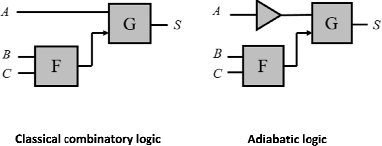
Figure 7.27. Classic logic and adiabatic logic
The same function cannot be performed in the same way, as in an adiabatic gate, the signals need to be synchronized at the input, which is not the case for classic combinatory logic. In the example given, it is necessary to add a “buffer” to resynchronize the signals. This technique can result in a large amount of supplementary gates being added to a circuit, which can then bring about an overhead in terms of consumption.
7.4.2. Adder example
The adder is a basic function of binary arithmetic. All of the more complex functions such as multiplication, Fourier’s transformation and digital filters are performed using binary adders as a base. The properties obtained on an adder are fairly representative of the properties that are obtained in any digital circuit. Moreover, this function is an excellent educational example. Figure 7.28 shows the classic structure of a four-bit adder. The logical equations to be implemented for the i bit are:

The variables a and b are the input bits and c is the carry bit. The F function performs the two logical equations above. The number of buffers in overhead is 18 and has to be compared with the four blocks performing the logical functions themselves. The circuits delaying two bits are counted as two buffers. The circuit latency is the four gates propagation delay. It is quite easy to show that, generally, the adder with N bits, the buffer overhead and the latency are respectively:

The adiabatic adder schema is as follows:
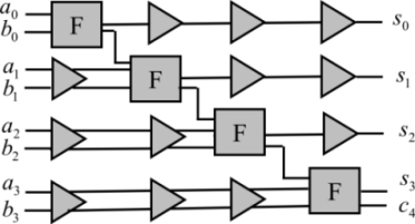
Figure 7.28. Four-bit adiabatic adder
The number of circuits to be added increases significantly with the number of bits and it can become prohibitive. In the case of the adder, a possible solution is to separate the circuit into k adder circuits, each operating on N/k bits. Each adder block of reduced dimension is implemented twice, corresponding to the two possible values of the carry of the previous block. An output circuit processes the outputs of the k adders. It can be shown that the number of additional buffers for the k adders is:
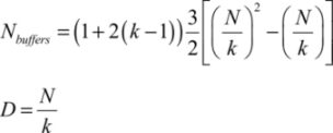
The output circuit requires a number of  for the multiplexers and a number of
  for the buffers.
Improvements to the performance are made to the detriment of the surface increase. There is an optimum relative to the dissipation for significant values of N. For example, for N=64, the optimal value for k is 8.
Other adder architectures have been proposed in the literature: the Sklansky adder, the Brent–Kung adder, that of Kogge–Stone and that of Han–Carlson. Their performances, however, differ very little to the fragmented optimal adder described earlier. When compared with classical CMOS performance, we note that there is a reduction in dissipated power by a factor of four when using optimized structures. These results are once again further away from the theoretical performance.
7.4.3. The interest in complex gates
The last section in this short introduction to adiabatic architectures demonstrates the interest in gates that reduce a micro-pipeline’s depth and, consequently, the number of buffers and also dissipation. This subject has not been widely explored in the literature. Figure 7.29 shows a complex OR gate with N inputs.
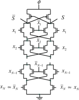
Figure 7.29. Complex exclusive OR gate with N inputs
The reduced number of micro-pipeline stages allows the number of synchronization buffers to be reduced, as well as the dissipation. However, there is an increase in capacitances. Complex gates can also serve as a basis for performing adders.
In conclusion, this chapter defined the structure of adiabatic gates that are compatible with CMOS technology, which can bring about a four-factor power decrease. However, performance is still very much below the gains that can theoretically be achieved for two main reasons:
– The existence of sub-threshold voltages in CMOS technology provokes a non-adiabatic dissipation of  which is far greater than adiabatic dissipation in the form
  . Note that this phenomenon is intrinsically linked to the physics of a field-effect transistor and can only be marginally improved with technology.
– There is a need to move to a micro-pipeline-type structure, which adds elements to the logic gates that are necessary for performing logical functions whose only function is to delay the signals.
New components need to be used to bridge the first limitation. Chapter 8 will present an emerging technology that is based on nano-relay. New solutions on the architectural level, which go beyond the principles outlined in this chapter, will be discussed in the conclusion to this book in the form of new avenues to address the second limitation. We will also take note of the limits that supplies can bring to energy recovery, and we will discuss the advanced technological possibilities in this domain.


