3
Transistor Models in CMOS Technology
This chapter explains the physical phenomena implemented in CMOS technology from the standpoint of assuming that the reader has a basic knowledge of semiconductor physics. It aims to give an improved understanding of the effects that technological parameters have on current’s values and equivalent capacitances. Furthermore, it will allow us to analytically calculate heat dissipation in logic gates. This chapter also aims to give more detailed explanations of what was briefly outlined in the first chapter of this book.
3.1. Reminder on semiconductor properties
3.1.1. State densities and semiconductor properties
3.1.1.1. Electrons and holes
The electrical properties of semiconductors, in contrast to the metal properties, include not only electrons, but also holes. The holes are not particles, but a very convenient representation of the properties of certain electrons in the semiconductor. They are equivalent to particles that have an opposing charge to the electron, but a similar mass. In semiconductor physics, the mass is replaced by the effective mass, which is a quantity that is more directly accessible when writing transport equations. While electrons and holes have different effective masses, they are in the same scale.
3.1.1.2. State densities and Bloch functions
A knowledge of both the laws that explain the density of carriers (electrons and holes) and the laws explaining currents at a macroscopic level is sufficient prior knowledge for understanding the properties of semiconductor-based components. It is nevertheless, also informative to understand the origins of these laws based on fundamental physical models. This book will be limited to a brief introduction to this, but there are references made to other cited publications [ASH 76, TSI 88, MAT 09], which give a much more thorough explanation of these rather complex phenomena.
The physical basis for all of these is what is called the band theory in a solid model. This model is based on quantum mechanics and describes the physical state of conduction electrons in a periodic space. The possible states mentioned herein are the conduction electrons’ states, meaning those electrons that are peripheral and loosely linked to the atoms. They are considered indiscernible and have a half-spin, which obeys the Fermi–Dirac statistic. Although the only physical representative size is the state function of the population of conduction electrons as a whole, knowing the individual states of electrons can help us to understand various semiconductor properties. This book will not make much use of band theory, as electromagnetic and state density equations, as well as simplified conduction equations, on their own enable us to establish electrical models of transistors. However, this does remain a central theory and some basic notions of it are given in this introduction.
In the Schrödinger picture, the states of conduction electrons are represented by wave functions that take on particular forms in a crystal. They are called Bloch functions and are given by the following equation:

In this equation, r is the vector position of the electron in the solid and k is a physical vectorial quantity called the wave vector, for which the classical equivalent is the impulsion to factor ħ, the quantity ħ is Planck’s reduced constant, which is equal to 1.05.10−34 Js, E is the electron’s energy, t is the time, the function unk(r) is a periodic function in space, and n is the degeneration index, as many electrons may have the same energy.
3.1.1.3. Energy bands and Fermi energy
The solution to Schrödinger’s equation in the crystal allows a relation to be written between the energy and the wave vector, which is called the dispersion relation. This relation is often represented graphically and is called a band diagram. Effectively, all of the energy values are not possible and all of the authorized values are grouped into bands. This conclusion can be arrived at by using Schrödinger’s equation. The possible energy values are represented by different directions of the vector k in the reciprocal space, the Fourier transform of the real space.
Figure 3.1 shows the diagram of silicon bands using the directions (1 1 1) and (1 0 0) in the reciprocal space. The reader is encouraged to consult publications on physics [ASH 76] for further details concerning this rather complex representation. The two directions can also be recognized by the letters Γ Δ Χ for (1 0 0) and L Λ Γ for (1 1 1). There may be many energies corresponding to the same value as k.

Figure 3.1. Silicon-bands diagram
In Figure 3.1, the energy values shown in the gray area are forbidden. The width of this area is the “gap”, the basic quantity in semiconductor physics. It is 1.1 eV for silicon. The loosely linked electrons in the crystal fan-out and occupy the possible states, according to this diagram. In order to understand how they are distributed, it is necessary to recognize that all of the values of k are impossible, but that a gap of 2π/Lx separates the two consecutive values of kx for the projection on the axis of x. This is also the case for the two other projections on y and z.
According to Fermi statistics, the electrons divide by giving preference to occupying the weakest energy states. As many electrons cannot be in the same quantic state, the bands fill up and a maximum energy level has been attained when all the available electrons have been assigned. This level in the solid is called Fermi energy, and it is a very significant quantity.
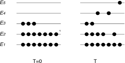
Figure 3.2. Filling in the bands and the Fermi level
Figure 3.2 symbolically represents how the electrons are positioned according to the possible levels in both cases: null temperature (absolute zero) and non-null temperature. The Fermi level is the energy E3 at absolute zero. The distribution of electrons at non-null temperature is expressed as the density of probability p(E) to find an electron in an energy state between E and E+dE:
In this relation, we recognize Boltzmann’s constant and Fermi energy EF. It can be shown that Fermi energy is also the chemical potential as defined in the systems’ thermodynamics, exchanging particles with the thermostat. It is expressed as:
In this relation, U is the system’s internal energy, N is the number of particles, and S and V are the entropy and volume, respectively, which are assumed to be constant.
Figure 3.3 illustrates a more intuitive version of the bands, which allows notions of conduction bands, valence bands and holes to be introduced. The diagram shows which energies are accessible, according to their position within the solid. The highest band is called the conduction band and the lowest is the valence band.

Figure 3.3. Bands and the notion of holes
The diagram on the left represents the states occupied and the diagram on the right shows the possible states and the effectively occupied states. In order to obtain the curves of the possible states, it is necessary to express the energy according to the wave vector and to determine the states’ densities for a given energy, taking into account the quantification of the wave vector’s values. This classic solid physics calculation gives the following values as a result of the possible state densities by volume unit:
In these relations, the quantities me∗ and mh∗ are the effective masses of the carriers, as defined by the dispersion equation. They play the same role as the mass in the classical dynamic equation of charge movement, which explains the name “effective mass”. The values in silicon are, for example, 1.06 m0 for the electrons and 0.6 m0 for the holes, where m0 is the mass of the electron. To determine which states are effectively occupied, it suffices to multiply the states’ densities by the Fermi function, as has been explained at the beginning of this chapter.
In the valence band, the graph does not represent the occupied states, but the states that are not occupied, which explains the term “hole”. In practice, the hole is considered to be equivalent to an electron, but with a positive charge and a different mass. The hole is in fact not another particle, but equivalent to the absence of electrons in the quasi-full band.
These notions may seem counterintuitive when read for the first time, but they are indispensable to understanding the conduction of a semiconductor. Therefore, two particle populations co-exist: electrons with a given effective mass (different to that of free electrons), and pseudo-particles called holes, which can be considered as positively charged electrons, which are strictly opposed to that of an electron with their own effective masses.
3.1.1.4. Carriers’ densities
Starting from the expression of the Fermi law, we easily understand that the position of the Fermi level and the integral values of carriers’ (electrons or holes) densities are easily linked. The densities of electrons (n) and holes (p) are given by the following relations:
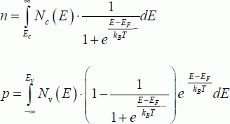
A calculation of these integrals, which assumes that the exponential terms are far greater than one, leads to the following result:
These two relations are very useful for expressing the carriers’ density in an undoped semiconductor. In a pure semiconductor, the density of electrons in a conduction band is equal to the density of holes in a valence band, because a hole in the valence band corresponds to a passing electron in the conduction band. Therefore, it can be written that:

When the semiconductor is doped, meaning when boron, phosphorous or arsenic atoms are introduced, other electrons or holes become unlinked and available for electrical conduction, as shown in Figure 3.4.
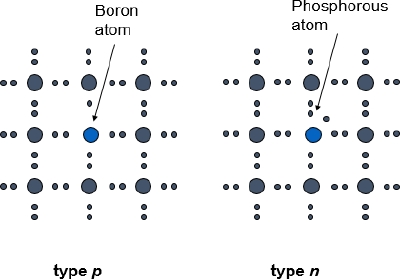
Figure 3.4. Doped semiconductor
It is quite natural to assume that all phosphorous atoms provide a conduction electron and that all boron atoms provide a hole in valence bands. As the charge remains the same, it is possible to write:
Type n doped semiconductor: n = ND + p
Type p doped semiconductor: p = NA + n
In these relations, the dopant densities are expressed as ND and NA. In practice, there are few holes in a type n semiconductor and n ≈ ND. Moreover, there are few electrons in a type p semiconductor and p ≈ NA. Implementing these electrical relations and density expressions according to the Fermi level leads to the following depiction in Figure 3.5.

Figure 3.5. Doped semiconductors
It is rather convenient to be able to express the concentrations off carriers in doped semiconductors according to those of intrinsic semiconductors. In this case, the hole density and the electron density are equal. Therefore, it can be written that:

This common value is noted as ni. At room temperature, its value is approximately 1010/cm3.
In this case, it can be deduced that the value of EF is written as Ei:
In an intrinsic semiconductor, the Fermi level is approximately in the middle of the forbidden band. The concentration of carriers for a doped semiconductor is written as:
These equations will be used further on. Note that ni is a quantity that is dependent on both the temperature and the semiconductor gap, but remains constant in a device. The energetic quantities Ei and EF vary according to the position:
A very useful property is to link the variation EF and the applied potential difference. Taking into account the fact that Fermi energy is also a chemical potential, it is possible to demonstrate that the Fermi level difference between the two regions (A and B) at equilibrium is such that:
VA − VB is the applied potential difference between the two regions A and B.
The variations of energy Ei can easily be deduced from the conduction and valence band variation and levels, as this energy is approximately equal to (Ec − Ev)/2. Equation [3.11] is fundamental to understanding how semiconductor devices function. It allows us to position Fermi levels according to the applied voltages. The conduction and valence bands are then positioned in accordance with dopants and the gap value. In certain cases, the Fermi levels will be replaced by Fermi pseudo-levels as separately defined by electrons and holes.
3.1.2. Currents in a semiconductor
Calculating the current in a semiconductor-based device is the basic calculation for modeling devices. Conduction in solids theory is very complex, but in order to create an operational model of the first order, we will restrict ourselves to a simplified approach, which consists of breaking the current down into two components: the diffusion current and the conduction or drift current. The density of the current linked to the electrons through a surface can be expressed by the following equation:
In this equation, the first term corresponds to the applied electric field effect. The coefficient μn is the assumed constant mobility of electrons, for rather weak (approximately less than 1 V/μm) electric fields. In silicon, its value is 1,350 cm2/(V·s). The second term corresponds to the carrier diffusion. The diffusion coefficient is linked to mobility by Einstein’s equation:
The quantities n and e are the density of conduction electrons and the absolute value of elementary charge (1.6.10−19C). An identical equation for the holes can be written as:
The mobility of holes in silicon is approximately three times weaker than that of electrons. The values for the densities n and p are given in the equations in the previous section.
One last useful equation is expressing the current according to the Fermi level. With the particular expressions of n and p in the semiconductors at equilibrium, the following equation can be obtained:

As defined by the conduction band:

The energy that varies is only the electrical potential energy because the kinetic energy remains constant at constant temperature. By combining these two equations and the equation that gives the current total, it is easy to obtain:

More generally, the currents of electrons and holes are:
In certain cases, we must define two different Fermi levels for electrons and holes, assuming that the two populations are at equilibrium. These will be called Fermi pseudo-levels. These formulas establish a particularly simple relationship between the current and the Fermi level variation.
3.1.3. Contact potentials
More often than not, electronic devices are composed of different dopant semiconductor parts, as well as insulating and metal parts. Therefore, there is always a contact with different materials and it is very important to understand the electrical phenomena in the interfaces. These phenomena are also very complex, as the chemical composition of interfaces is not always well known. However, the contact potential method is quite a simple way to incorporate the contact properties into the components models.
When the two different materials are put into contact, the carriers (electrons or holes) are generally diffused from the material in which the carriers are most numerous to that in which they are least numerous. This charge movement leads to the creation of a charged area and then a potential electrical difference. This difference in potential is the contact potential.
We will assume that this difference in potential only depends on materials in contact, and perhaps also the temperature. When one of the materials is a semiconductor, it also depends on doping. It is also useful to measure the contact potential of any material expressing the potential difference which appears when it is put into contact with the intrinsic silicon. It will be noted as ϕ.
When the material is a type p semiconductor, putting it into contact with an intrinsic semiconductor will lead to forming a junction and the appearance of a potential difference, given by:
This equation, which depends on the doping NA of a type p semiconductor, is demonstrated in publications that deal with component physics.
For a type n semiconductor, the contact potential is:
When the material is a metal, the contact potential only depends on the metal. A few values have been given in the table below:
| Material | Contact Potential |
| Silver | 0.4 V |
| Gold | 0.3 V |
| Nickel | 0.15 V |
| Aluminum | 0.6 V |
| Copper | 0 V |
The contact potential between any two materials 1 and 2 is easily calculated by interposing intrinsic silicon between the two materials. Thus, it can be written as:

The same method allows the case of n materials in a series to be processed:

3.1.4. Metal-oxide semiconductor structure
This is truly the base structure for CMOS technology and the majority of the properties of this technology can be deduced from it. The basic principle is to control the charge in a semiconductor, by applying a voltage through a thin oxide layer. This is the main principle of field-effect transistors, which is the basic component of all digital electronics.
The structure is composed of a doped silicon base, also called the body, an oxide (for example, silicon dioxide) and a metallic electrode. If needed, an electrode in contact with silicon can be added. A gate voltage is applied between the metal electrode and the silicon block, as shown in Figure 3.6. There are no undoped silicon atoms shown in the figure. The circles are the doping atoms, which are type-p dopants in this case. The black dots represent the electrons and the + signs are the holes supplied by the doping atoms.
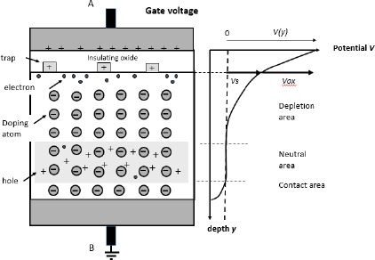
Figure 3.6. Metal-oxide semiconductor structure
When a positive voltage is applied to the gate, the semiconductor’s holes are pushed toward the ground and a space-charging area (charged area) is created under the oxide. In parallel, some of the conduction electrons of the semiconductor (some electrons are still present, even in a heavily doped type p semiconductor) are attracted by the gate voltage and they begin to form a fine layer on the oxide interface of the semiconductor. Although this is a very fine layer, it will have a major effect on the properties of the field-effect transistor. It is called an inversion layer because of the minority carriers. The model also takes into account the charged states, at the interface. This device is a kind of capacitor, and applying a positive voltage between the gate and the ground is equivalent to charging a capacitor.
In the first stage, the voltage Vext is applied between the gate connection (A) and the substrate connection (B) according to the different electrical potentials of the device.

By introducing the contact potentials, we obtain:

Assuming that the contacts A and B, the gate electrode and the rear-facing electrode are made using the same material, the equation is written as:
The potentials are measured with regard to that of the semiconductor in the neutral area, which is used as a reference.
When the voltage increases, a film of electrons is formed at the interface of the semiconductor, which further increases the electron layer. This plays the role of an electrostatic screen and surplus voltage is integrally applied into the oxide. Similar to the capacitor, a positive charge is created at the electrode interface of the oxide gate.
Following the analysis is a calculation of the potential in the device given by an applied voltage. This is a rather complex calculation and readers who are not so interested in the finer details should skip ahead to the results and discussion at the end of the section. The calculations are based on the expressions of carrier densities according to the Fermi level EF and the level Ei(y). We notice that the Fermi level is constant because no current circulates y:
The potential V(y) is conventionally measured with regard to the neutral area in the silicon block called the “bulk”. Taking into account the fact that:

The following expressions by concentration are obtained:
In the neutral area of the semiconductor, it is written:

Poisson’s equation allows the basic structure equation to be obtained:

After having multiplied the two terms by dV/dy and replacing the densities with their expressions, finally we obtain the following:
In this expression ϕt is equal to kBT/e, and its value is 26 mV at room temperature. In this expression, ϕF is called the Fermi potential of the substrate and is defined by:
For a type-p semiconductor, it is equal to:
For a type-n semiconductor, it is equal to:
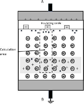
Figure 3.7. Calculating the inversion charge
The following calculation consists of finding the inversion charge’s expression, as this charge is the main cause of conduction for the microelectronic field-effect transistors.
It is possible to calculate the electric field in the structure, in particular at the oxide semiconductor interface level. Applying Gauss’s theorem to the volume depicted in Figure 3.7 allows us to write:

The charges per surface unit  and
and  are, respectively, the charge of the inversion layer and the charge of the depletion area.
The generally applied equation of y=0 can be simplified by assuming that  is far greater than one. This estimate is legitimate as Fermi’s potential does not vary much under doping and takes a value between 0.2 and 0.6 V, values much higher than 26 mV:

It, therefore, follows that:

The value  is easily calculated by applying Poisson’s equation to the neutral area and assuming that the inversion charges are located very close to the surface:

From this, we can deduce that the inversion charge is:
Thus, the inversion charge varies exponentially with the surface potential Vs. Still to be established is the link between the surface potential and the voltage applied between the gate and the ground. A three-equation system enables the problem to be completely resolved. The first equation is written as:

In this equation, which expresses the charge conservation in the total volume, the charge of the gate electrode  and the charge of the surface defects are integrated into the interface. The equation for conservation of the total charge is deduced by applying Gauss’s theorem to the total device. The other two equations are:


The first equation is the same as equation [3.20] given at the beginning of this section and the second is the classical relation of the flat capacitor formed by an oxide layer. Finally, by grouping together the four previous equations, we obtain:
This very general equation has no analytical solution, but it can be expressed more simply in the two functioning regimes: the strong-inversion regime and the weak-inversion regime. These two regimes are fundamental to understanding transistor functioning.
3.1.5. Weak and strong inversion
3.1.5.1. Strong inversion
Let us use equation [3.31] again, which expresses the surface charge. When the surface potential is greater than 2ϕF, it varies very quickly. The surface potential does not vary much due to the surface charge, nor does it vary much due to the applied voltage when it is sufficiently high. This hypothesis is confirmed by the digital simulations, but it is possible to draw the same conclusion if we consider the inversion layer as an electrostatic screen. Above a certain value, all excess voltage is applied to the oxide and not to the semiconductor. The constant value of the surface potential is chosen to be 2ϕF by certain authors, based on the exponential term of formula [3.31]. Others choose a higher value by adding 6ϕt. Let us take the equation system again, with  as unknown:


From this, the value of the inversion charge in the strong-inversion regime is deducted:
The quantity VT is called the threshold voltage and it is fundamental in field-effect transistor models. It is expressed as:
We recall that the surface potential is constant and in the order of 2ϕF. We also note that the definition of threshold voltage is a bit arbitrary, as the formation of the inversion layer is a continuous process. The applied potential must, therefore, bridge a certain amount of barriers before the inversion layer is formed: the contact potential ϕMS, then the potential coming from the surface charges  , then the silicon barrier Vs and finally the barrier of the deserted area. This last barrier is also called the “body effect” in the literature. It shows the effect that the deserted area has on the value of the threshold voltage.
3.1.5.2. Weak inversion
In the weak-inversion mode, the applied voltage is weaker. The surface potential remains greater than ϕt but less than 2ϕF. In general equation [3.28], the following term is defined:

This term is considered as infinitely small, which enables the limited development for the expression of the charge. Thus, the following equation can be obtained:

or
Again, the equations of this problem can be written as:


Then, an equation of the second degree is obtained in  if we assume that the inversion charge is much less than the charge
  :
:

In this expression, the coefficient γ is equal to:
This is the same coefficient that intervenes in the “body” effect. Although it would be possible to resolve this second-degree equation, for the sake of simplicity let us assume that the surface potential remains constant with the value 1.5 ϕF, for example. We will also linearize the function expressing the surface potential according to the applied voltage.
The threshold in a weak inversion VX is defined by:

We obtain:

The coefficient n0 is given by:

Therefore, the inversion charge can be expressed based on the equation given at the beginning of the calculation:
This equation characterizes the weak-inversion regime, which is also sometimes called the sub-threshold regime. This analysis requires many approximations. Note that there is a certain arbitrariness concerning the hypotheses made on the potential surface value. Nevertheless, the overall tendencies are well described by this model. We also note that the threshold voltages as defined in strong and weak inversions are not strictly equal. They are often confused in the literature on the subject.
Threshold voltage in a strong inversion:

Threshold voltage in a weak inversion:

Based on the general equation that gives the value of the surface potential in a weak inversion,

It is possible to calculate the derivative of the gate voltage with regard to the surface potential:

It is then very easy to verify that this factor is equal to:
The capacitances Csi and Cox are the capacitances of the depletion area and of the capacitor formed by the oxide layer, respectively. This coefficient, called the sub-threshold slope, plays a very important role in electronics and is equal to one at a minimum. It increases when the ratio between the depletion area capacitance and the oxide layer capacitance increases.
3.2. Long- and short-channel static models
3.2.1. Basic principle and brief history of semiconductor technology
Here we consider the basic component in micro-electronics today: the field-effect transistor. Its properties were listed in Chapter 1; however, for us to know how it functions, we have to understand the physical principles outlined in this chapter. This first section aims to give a phenomenological description of field-effect transistors.
The first ever idea in the field was to control a wire’s conduction with a grid in the same way as a grid controls the current emitted by a triode’s filament, or how a tap controls the flow of water. An insulated wire would not work, as the current passing through an insulator is at absolute zero. A conduction wire did not seem to be a very convenient method either, as the field does not penetrate in a conductor. Therefore, it was difficult to envisage a control method for this case. The semiconductor appeared to be a good material, as it offered the two basic properties: the possibility of letting a current pass through it and internal field penetration. The first device was invented and patented by Lilienfield in 1933.
These patents illustrate the general principle of controlling the conduction of a semiconductor. The material chosen for the semiconductor was copper sulfide, presenting a type-p behavior. There was no great future that followed this choice, but the basic principle had been laid out. These devices were of MOS types in depletion mode. The main principle of MOS depletion mode is to reject the carriers outside the conduction channel by applying a voltage. It was only in 1948 that Bardeen had the idea of taking up this principle again. This time, however, the carrier density was increased by applying a voltage, which created an inversion layer, meaning a layer formed by minority carriers.
In MOS enhancement mode, there is no longer a doped area that serves as a conduction channel. The holes in the base material cannot give way to a current because the two source–bulk and bulk–drain junctions are, respectively, non-polarized and reverse-polarized. Only the electrons can create a current in this type of device. When a voltage with a value of absolute zero is applied to the gate, the electrons are not injected into the semiconductor and no current circulates from the source to the drain. When a positive voltage is applied to the gate, it attracts electrons supplied by the source and drain. A current can then be established.

The micro-electronics industry has been progressively abandoning MOS depletion transistors and replacing them with MOS enhancement transistors, as they are much simpler to make. Furthermore, MOS enhancement transistors allow very low-consumption circuits to be implemented, which has paved the way for CMOS technology, with which the majority of integrated circuits today are made.
Channel n devices are not the only devices to be made. Equivalent devices can also be made by playing on the conduction of holes. The channel is, therefore, of type p. In this case, a negative gate voltage is applied, in order to enhance the channel. These two enhancement transistor types, MOS channel n and MOS channel p, are the two building blocks of CMOS technology.
Let us now study how enhancement transistors work. Figure 3.9 uses the example of MOS enhancement functioning and explains how the conduction varies when different voltages are applied.

Figure 3.9. NMOS transistor functioning
In the first step, the gate is at absolute zero voltage and the drain is positively polarized. As seen in Chapter 3, no electron is confined to the insulating semiconductor interface, and hence, there is no current. MOSFET is non-conductive.
When a positive voltage is applied to the gate, an inversion layer forms and it goes from the weak-inversion regime to the strong-inversion regime as the gate voltage increases. This phenomenon appears when the gate voltage is greater than the threshold voltage on the scale of 0.3 V. The electrons are supplied by the source and a current can circulate from the source to the drain under the electric field effect present in the device. MOSFET is conductive.
If the gate voltage remains constant and the drain voltage increases, the potential difference between the gate and the channel area near the drain may become less than the threshold voltage. The charge of the inversion layer is, therefore, absolute zero at the end of the channel. This last regime is called a saturation regime. The channel can be considered as a series connection of a weakly resistant conduction area and an inverse-polarized junction. Any further increase in the drain voltage translates into an increase in the voltage at the terminals of junctions p and n at the end of the channel. No increase in the voltage can be expressed at the terminals of the conduction channel. The drain current remains constant.
The geometry that has been previously described is in fact a very simplified version. The real geometry is shown in Figure 3.10. The channel length is very weak, less than 90 nm in the most advanced technologies. The oxide thickness is a few nanometers, so that the influence of the gate is maximized. The exact transistor width is defined by the circuit designers, but it is always less than a micron in digital technologies.

Figure 3.10. Transistor in CMOS technology
3.2.2. Transistor architecture and Fermi pseudo-potentials
The structure of field-effect transistors is based on the metal-oxide semiconductor structure, but there are some significant differences between the two, due to the two electron pools on both sides of the channel. Figure 3.11 depicts these differences and is useful in writing about the concentration in this new structure.
The problem becomes a two dimension problem and the thermodynamic equilibrium is no longer completely ensured, because a current is circulating in the device. Two Fermi pseudo-levels are defined, one for the electrons and another for the holes. They both play the same role as a Fermi level in a semiconductor at equilibrium.

Figure 3.11. Calculating the concentrations in a transistor
The concentrations of electrons and holes are written as:

The fact that the Fermi pseudo-level depends only on the position in the channel, not on the depth, expresses that the carrier fluxes are compensated in the y dimension, and not in the x dimension. To understand this, we have to recall the relationship between the variation of the Fermi level and the current. By including the Fermi pseudo-level, the below is obtained:

The first term is the Fermi pseudo-level difference between electrons and holes. It is noted that  shall not be confused with the electrical potential. The second term EFp(x) − Ei(x, ∞) is, by definition, of the Fermi potential −eϕF. The notation (y = ∞) expresses the position in silicon far from the interface. The last term is −eV(x, y,) in which the electrical potential V(x, y) is measured with regard to the “bulk”. In a definitive way, we obtain:

In the metal-oxide semiconductor structure, the density of electrons is given by:

We apply this equation at the source level, the difference in Fermi levels is the applied potential difference, multiplied by the inverse of the elementary charge. We obtain:


By writing the same equation in depth for the semiconductor p, we obtain:

Likewise, the density of electrons is written as:

Another way in which to write the electrons’ density is:

The density of holes remains unchanged with regard to the metal-oxide semiconductor structure, as the holes are not exchanged with the exterior:


The general equation that gives the potential is slightly modified when compared with that established for the metal-oxide semiconductor. As for the source, it is written as:
With regard to the drain, it becomes:
3.2.3. Calculating the current in a long-channel static regime
This is the simplest model for determining the current circulating in the channel. It is based on the equations outlined in the previous section. The calculations are done by considering the current to be the sum of infinitesimal portions dID and then integrating over the whole depth of the conduction channel. The width of the channel is written as W and the expression of the current (sum of the drift current and the diffusion current) results from formula [3.13] given in section 3.1.2:

with

The density of electrons deep within the bulk n (x, ∞) is a constant observed to be equal to  :
:

Taking into account the fact that the Fermi pseudo-levels do not depend on y, it remains as:

By integrating over the whole depth of the channel, we obtain:

As the current is conserved in the channel, this constant value can be calculated by:
These equations are quite natural as the current in a established regime is the derivate of the conduction channel with respect to the time. We recall that the term VCB is the difference between the Fermi pseudo-level of electrons in the inversion layer and the Fermi pseudo-level of holes in the semiconductor.
In order to go further in the calculations, we must integrate this equation over the potential. When fundamental equations [3.32] and [3.33] are transposed to the full transistor, the inversion charge and VCB can be expressed according to the surface potential Vs:
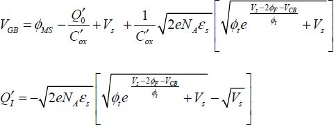
Therefore, the variable needs to be changed in the integral, which expresses the current. The calculations for this are, however, very complex.
In the strong-inversion regime, the problem becomes greatly simplified because we can show that the relationship between VCB and Vs becomes:
The quantity ϕB slightly varies in the strong inversion, and it is generally chosen as 2ϕF. The equation giving  explains this estimate. Let us take the results obtained in section 3.1.5 again:

With these estimates, the current then becomes:

Calculating this integral then leads to the following equation:
In this equation, the parameters VFB and γ are defined by:
This very general equation allows the saturation phenomenon to be explained. When the voltage VDS increases, the current starts growing less and less and the derivative ends up cancelling itself out. This saturation phenomenon corresponds to the fact that, as the voltage increases, the voltage between the channel and the drain ends up being less than the threshold voltage at the drain level. The channel then becomes insulating at the drain level and an excessive increase in the voltage does not translate into an increase in the voltage at the terminals of the channel’s conducting part. Figure 3.12 illustrates this phenomenon.
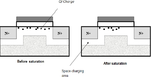
Figure 3.12. Transistor saturation
A simple way to calculate the drain’s current consists of estimating the last term’s value at around VSB + 2ϕF and neglecting the terms depending on γ. Then, we obtain the well-known equation:
In practice, these equations are the most used. They show that the threshold voltage varies when a voltage is applied between the source and the “bulk”. This effect is often referred to as the “body effect” in the literature.
When the derivative of the current is zero with respect to VDS, the saturation VDSsat can easily be found:

Another way to write the current is using the parameter α as defined by:
The current can be written concisely as:
Figure 3.13 shows the current circulating in the transistor according to the voltage applied between the drain and the source for different voltage values, applied between the gate and the source.
For the channel transistor p, the calculation is identical, even with a certain amount of sign changes. We maintain that reversing the voltage equations is enough. For example, the VDS voltage will be replaced by VSD. The PMOS threshold voltage is negative, but only the absolute positive value is used. Therefore, it can be written that:
In this case, the circulating current from the source to the drain is counted as positive. All the voltages figuring in this formula are positive.
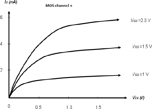
Figure 3.13. Characteristic curves of a channel n transistor
3.2.3.1. Calculating the current in weak inversion
The weak-inversion regime corresponds to the weak values of the voltage applied between the gate and the source. In the micro-electronics of today, it is very important to know the factors that contribute to forming this current. In digital logic gates, NMOS transistors are cut when a voltage of absolute zero is applied between the gate and the source. The circulating current has a weak value, but is not at absolute zero. In a logic circuit involving millions of gates, millions of currents of this type are circulating and contributing to dissipation. The following analysis indicates that this value is significantly more important when the threshold voltage is weak, which is exactly the case for advanced technologies functioning at low voltages and weak threshold voltages. PMOS transistors have exactly the same problem. A positive voltage applied between the source and the gate blocks the transistor without reducing the current to zero. These undesirable currents are called subthreshold currents and their effects should be minimized.
As we have already done with strong inversions, let us use equation [3.34] of the inversion charge, taking into account the presence of the source and the drain. At the source level:

At the drain level:


We assume that the drift current is negligible compared with the diffusion current. The density of the inversion charges is indeed weak in this regime:

Section 3.1.5 allowed us to establish that:

The electrical potential is the solution to this second-degree equation:

The potential is constant throughout the channel. We obtain:

By replacing the inversion charge at the source level with the value obtained in section 3.1.5, we arrive at:
with

Written more classically, the current uses the threshold VT instead of VX. Note that the threshold in the weak inversion is slightly different from that in the strong inversion:
with

By integrating the equation established in section 3.1.5, it can be written that:

An equivalent expression is obtained:
Other expressions are sometimes used in the literature, particularly that of the BSIM model, which has been better adapted to advanced technologies:
In the following section, we will describe in detail another term that depends on the voltage between the drain and the source, in order to take into account the short-channel effects. The value of the coefficient η is approximately 0.1.
In each case, there is an exponential dependence between the sub-threshold current and the threshold voltage. The more the threshold voltage diminishes, the more the drain current increases. This property is fundamental because when the transistor is blocked, meaning when the gate is at zero, the residual value of the current, called the sub-threshold current, is as weak as the threshold voltage is elevated. This property explains the fundamental limits of CMOS technology in regards to very low consumption.
3.2.4. Calculating the current in a short-channel regime
Three effects are studied herein, which are all very significant in current CMOS technology:
- – velocity saturation of carriers;
- – reduction in the effective channel’s length;
- – reduction in the effective threshold.
3.2.4.1. Velocity saturation
In the previous calculation, the carrier speed was assumed to be proportionate to the electric field. When the conduction channel diminishes, this proportionality is no longer verified and the velocity tends toward a limited value, which depends only on the semiconductor and is called velocity saturation, written as vsat. This limited value of silicon is in the scale of 107 cm/s. The relationship between the velocity and the field is written as:
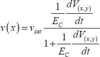
Assuming that the conduction layer is infinitely thin, the potential can be confused with the surface potential. By neglecting the diffusion part of the current, we obtain:
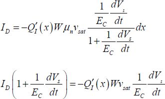
The current can be calculated by finding an average between the source and the drain:

The drain current in a short channel is corrected by the term  :
:
This equation is valid in an unsaturated regime. In a saturation regime, the derivative of the current with regard to the voltage between the drain and the source becomes absolute zero and:
The short-channel effect diminishes the saturation voltage compared with the long-channel value VGS − VT. We also note that a differentiation must be made between the saturation regime and the speed saturation under the short-channel effect.
When the channel becomes very small, the term VDS/LEC is far greater than unity, and the current becomes:

When the saturation voltage is overlooked, the current is simply written as:
The critical field value is in the scale of 2 V/μm for the electrons and 4 V/μm for the holes.
3.2.4.2. Diminishing the length of the effective channel
In the saturation regime, any increase in the voltage between the drain and the source translates into an increase in the deserted area at the drain level. This is because a surplus voltage is integrally applied in this area, as has been explained previously. The electrical length of the channel diminishes, which brings about an increase in the drain current. If we observe Figure 3.13, there is a slight slope beyond the saturation voltage that expresses this effect. This effect is all the more significant as the channel is short, because the relative variation is strong.
3.2.4.3. Diminishing the effective threshold
When the channel is short, the direct influence that the drain voltage has on the channel carriers increases. The deserted areas at the levels of the source and drain are relatively more significant, which increases the space charge and the surface potential. The electrostatic gate control is much less efficient. This is called the drain-induced barrier lowering (DIBL) effect. This effect can be analyzed in detail by taking into account the bi-dimensional aspects of the electrical problem. The final result is equivalent to a diminished threshold voltage. This decrease is modeled in the following way:
In this equation, we can see the influence of the ratio between the dielectric constants of silicon and the oxide gate, as well as the ratio between the oxide gate width and the channel length. In the BSIM model, the term that expresses the DIBL effect is written as:
The value of this coefficient depends on the technology and the transistor size, but the scale is 0.1. This effect is important for estimating the sub-threshold current value.
3.3. Dynamic transistor models
Within circuits, voltages vary and the static model is insufficient. There are three different approaches explored below: the quasi-static model valid when the variations are relatively slow; the full dynamic model and, finally, the “small signals” quasi-static model, valid when the voltage variations are weak. This last model is often presented as the electrical transistor model.
3.3.1. Quasi-static regime
The main principle in quasi-static analysis is to consider the conduction current as constant in the channel. The equations obtained in the previous sections will be retained, but this time the applied voltages will have a time dependency. The basic model is shown in Figure 3.14.
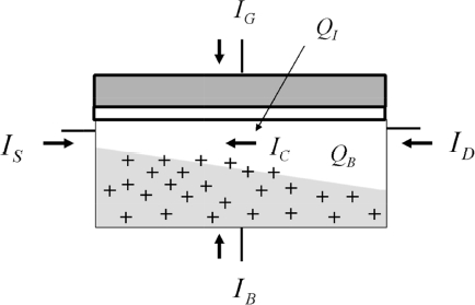
Figure 3.14. Quasi-static transistor model
The basic equations introduce the transitory currents IDV(t) and ISV(t):

The other terms are the static currents that were calculated in the previous sections, but this time embedding the fact that the voltages are variable in time. The transitory currents are introduced so that the varying phenomena in time are taken into account. Taking these transitory currents into account is necessary, as the conduction channel’s charge is not a fixed charge in the device. The component Ic(t) is the calculated current, being the sum of the diffusion and drift currents.
The following calculation allows us to understand the origins of these currents. In the first step, we forget the quasi-static regime hypotheses in order to establish the general equations on the total currents in the strong-inversion regime. By applying the charge conservation law to a conduction portion in the channel, it can be written that:
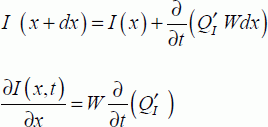
The current is given as:

Furthermore, in strong inversion, it is:

From this, it can be deduced that:

As with I (0,t) = −IS(t), it remains:

By averaging from 0 to L and retaining the total current:

The first term is integrated by parts, which allows us to obtain the following equation:

By comparing this equation with the current definition equation ISV(t), it can be deduced that:

This conduction current’s additional term current ISV(t) translates the dynamic aspects of the transistor. In the static regime, it is absolute zero. The conductive current’s equation Ic(t) is given by the formulas in sections 3.2.1–3.2.4, considering that the applied voltages are time functions. At the drain level, we can establish a similar equation:
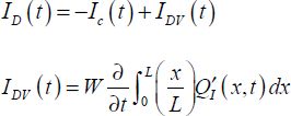
To determine the transition currents, we only need to replace  with its strong-inversion value. After some rather long calculations to include factor α as defined by using the simplified equation (ignoring the diffusion current) between dx and the current, it is possible to write:


These currents can be considered the derivatives of the source and drain’s virtual charges, defined by:
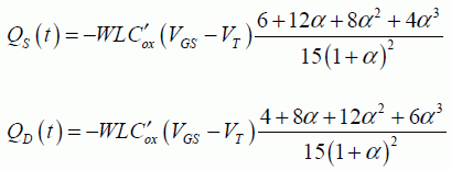
In the weak-inversion regime, the calculations are simpler because the surface potential is constant. It is, therefore, easy to show that the transition currents are negligible.
3.3.2. Dynamic regime
In practice, when the rise time of the gate voltage is not 20 times larger than the transit time of the carriers in the channel, the quasi-static regime hypotheses are no longer valid. Therefore, the following equation set must be resolved:

The unknown parameters here are the inversion layer’s charge by surface unit, the current, the potential and the surface potential Vs. The four equations allow the problem to be resolved. Note that the two last equations are only valid in the strong-inversion regime. The voltage depends on the time. There are other factors which come into play when writing the initial conditions, such as the continuously applied voltage. Solving this equation system is complex and digital techniques will need to be employed to do so.
3.3.3. “Small signals” transistor model
We start with the quasi-static transistor model. The equations given in section 3.3.1 help us to determine an electrical transistor model that we can use to estimate the circuit’s properties. Once again, we use the basic device equations:

These currents carry both a continuous component and a varying component, which is denoted by a lowercase. The transition currents are the components that vary in time, by definition:

We now add the gate and bulk currents’ transitory components iG(t) and iB(t).
These currents can be generally expressed according to the variable voltage components, and that allows us to write the following equations:

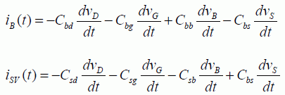
These equations are not independent. For example, four relationships can be written as:
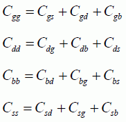
The first equation is obtained by writing that the drain’s transitory current iDV (t) is absolute zero when the four voltage variations are equal. The remaining three are obtained based on the same property as for the other three currents.
Four other equations are obtained by writing, for example:

In fact, when all the voltages are constant except vD, the general equations can be written and then the sum of variable currents will be written as absolute zero. It is the same for the other three voltages:
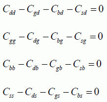
The system can be restricted to only three currents because the fourth current can be calculated by writing that the sum is absolute zero. Furthermore, the voltages are expressed relative to that chosen as a reference, such as the source potential, for example. Finally, we arrive at the following set of equations:
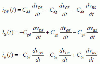
These equations lead to the equivalent diagram in Figure 3.15. A certain amount of simplifications is nevertheless necessary. We retain the same hypotheses of the quasi-static model. The calculations are not presented in detail in this book.

Figure 3.15. Small signals transistor model
There is more than just a minor likeness between this model and the set of equations shown above. The equations need to be written based on the model and it must be shown that they are equivalent to the general equations. The model’s parameter values, particularly the capacitances, are obtained by writing the charge expressions and derivating them with respect to the time. The expressions obtained in the static model are still considered valid in the quasi-static estimations. The current values are expressed from the conduction current equations. A very simplified expression may be:

Therefore, the parameter gm is  before saturation and
  in the saturated regime.
The parameter gd is equal to  before saturation and zero in the saturated regime.
These expressions are only valid in the long-channel regime, but are often found in the literature. Some more precise expressions are given in [TSI 88], [MAT 09] to process the short-channel effects.
The general equation which establishes a link between dx and dVCB will be used to calculate the total charges. Then, dx will be replaced by the values in integrals:

For example, the calculation will be broken down as follows:

The following relationships will be used:


The calculation is rather long and leads to:

The other charges are obtained in the same way.
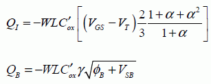
These expressions allow us to easily calculate the capacitances defined earlier:
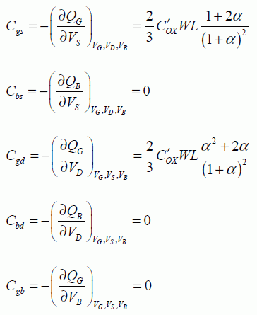
Note that the more detailed calculations will allow us to obtain the non-absolute zero values, which are shown as being equal to zero. Remember that these values are only valid in the strong-inversion regime. In the saturation regime, giving α a value of absolute zero is enough.
In order to find more precise expressions, it is necessary to first define the following parameter:

Thus, we obtain:
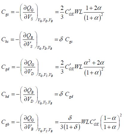
These approaches must be frequently modified. Those interested are encouraged to consult some specialist publications [TSI 88] to find out more.
To conclude this chapter, it is useful to know the scales of different parameters introduced in this chapter. Table 3.2 outlines the most important scales in CMOS technology: a rather old scale (0.18 μm) and a more classic scale (45 nm). The transistors used as examples are not the technology’s smallest size and are thus more applicable to the analog and “buffer”-type functions.
Table 3.2. Transistor model parameters
| parameter | 0.8 μm | 45 nm |
| W (μ) | 10 × 0.8 | 50 × 0.045 |
| L (μ) | 2 × 0.8 | 2 × 0.045 |
| ID (μA) | 20 | 10 |
| VGS (V) | 1 | 0.35 |
| VDSsat (mV) | 250 | 50 |
| VT (mV) | 900 | 280 |
| C’OX (fF/μm2) | 1.8 | 25 |
| gm (μA/V) | 150 | 150 |
| gd (μA/V) | 0.2 | 6 |
| Cgd (fF) | 2 | 1.6 |
| Cgs (fF) | 23 | 4.2 |
| COX (fF) | 35 | 6.25 |


