1
Dissipation Sources in Electronic Circuits
This chapter explains the origins of how heat is created in electronic circuits, and details its two fundamental components: dynamic power and static power. Dynamic power is the heat that is produced by charging and discharging of the circuit capacitors when the logical states change, whereas static power is the heat that is dissipated by the Joule effect when there is current leakage, or when currents below the threshold circulate within the circuit’s components. To fully understand how these mechanisms work, we need to analyze the different types of logical circuit structures. For this reason, we have dedicated a whole section to this subject. Logic based on complementary metal oxide semiconductor (CMOS) technology, which is used in more than 90% of current integrated circuits, will be explained in detail. The general principles put forward in this chapter will give the reader a fairly simple global view of the different aspects of heat production in circuits, and will allow them to understand the most important developments in semiconductor-based technology for reducing consumption. The more theoretical aspects will be discussed in Chapter 2 and the more detailed components of CMOS technology will also be discussed in Chapter 3.
1.1. Brief description of logic types
1.1.1. Boolean logic
In computer, audiovisual and control-command systems, data is binary-coded. This is true not only for the numbers, but also for the letters and, by extension, the sounds and images. Information processing systems perform the operations, from the simplest (addition) to the most complex (Fourier transformation). All of these are done by manipulating two symbols that are traditionally called “0” and “1”. In control-command systems, decisons are taken according to the value of logical functions, for example the value of “AND” when two simultaneous events occur. The mathematical model used in each case is Boolean algebra, invented by the Irish mathematician George Boole.
The simplest function is that of a single variable f(A). Four different functions can be defined according to the possible values of a variable A, as shown in Figure 1.1.

Figure 1.1. Boolean functions with one variable
The third function is a copy of the variable, and the fourth is the inverter function, written as  .
.
For two-input variables, the number of functions possible is the most important, as there are 24 possible functions, as shown in Figure 1.2.

Figure 1.2. Boolean functions with two variables
The functions f2, f7 and f8 are very well known in electronics. They are, respectively, the AND, the exclusive OR and the OR functions. They are marked as:
- – AND function: A.B
- – Exclusive OR function: A
 B
B - – OR function: A+B
The symbols translate a certain analogy with decimal calculations. For example:

However,

The point, which is the AND Boolean symbol, is often omitted to simplify the script.
All of the following are very easily executed using Boolean functions: binary arithmetic functions (used in current processors) and classical operations (addition, unsigned or floating point multiplication). For example, the addition of the bit i in Boolean algebra is written as Si and Ci is the carry:
We can now transpose the functions to the material level. The two states “0” and “1” are represented by physical quantities: two electrical voltages, for example. When the two voltages have two possible values 0 and VDD, the same symbols “0” and “1” are assigned indifferently to the logical and physical values. We can talk about the two states in the same way: the “on” state and the “off” state. We also note that the logical states can be materialized by different physical quantities of the electrical voltage: for instance the magnetic moment or the polarization. When a logical function is materialized, it is called a logic gate.
Boolean algebra comprises a large number of rules that are shown in the Truth Tables for the functions in question. These rules allow us to simplify the logical expressions in the Truth Tables. It is no longer indispensable to memorize these techniques, as they are all now integrated into synthesis tools. Let us make an exception for De Morgan’s rules, which are often useful for understanding how data logic gates work:
The elementary demonstration is based on the Truth Tables.
The two Boolean function decompositions are called “Minterm” and “Maxterm”, which are directly deducted from the Truth Tables. The simplest way to understand that is to use the example of figure 1.3, as it can serve as a generalization.
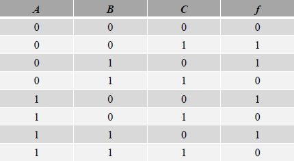
Figure 1.3. Example of a three-variable function
The Minterm decomposition is obtained by identifying the input values corresponding to a value of “1”:

The Maxterm decomposition is obtained by reversing this to identify the input values corresponding to the value of “0” as an output:

Reed–Muller’s decomposition is another decomposition that is fairly close to that of Taylor’s series function. It is based on the two equations given below:

Starting with the Minterm decomposition, it is possible to obtain an expression that only contains exclusive OR functions. Taking the example of the function given earlier, we obtain:

In this case, after simplifying, we obtain:

Generally, Reed–Muller’s decomposition presents the function as a sum within the exclusive OR of input variable products:
The factors are equal to 0 or 1.
To finish this introduction to Boolean algebra, let us introduce the notion of a Boolean function’s partial derivative:
This last notion, however, is not often used in the study of logical functions.
The decomposition of Boolean functions allows logical operations to materialize. Let us go back to the example given previously:

The basic “AND”, “OR” and inverter functions are assumed to be carried out by material blocks, which can be combined in any way. In practice, however, this property is not always guaranteed and the most frequent occurrence is where an output can only be applied to a limited number of inputs. This is what is meant by “fan-out”. The design of this simple function (Figure 1.4) shows the relative complexity of interconnect. This observation will be discussed in detail in the following section.
Knowing how many types of gates are necessary to carry out a particular function is a legitimate concern. The example given shows that the inverter, AND and OR functions are sufficient. In fact, we can dispense with the AND or OR functions by using De Morgan’s laws. The inverse function and the AND gate form the complete basis, from which we are able to generate all the possible functions. It is the same for inverter and the OR gate. Gates with more than two inputs can be easily performed based on two-input gates, but it is more useful to perform these gates directly if the technology permits.
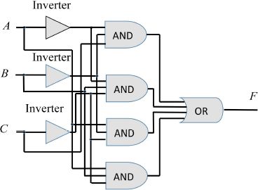
Figure 1.4. Boolean material architecture
To finish this brief introduction, we note that the NAND gate, that is to say the inverted AND, is enough on its own to generate all of the possible functions because if an input is permanently maintained at level “1”, it brings about the inverter function.
The logical function synthesis is a technique that will not be explained in detail in this book. The aim of the synthesis is to create a circuit using as few gates as possible and to minimize the delay between the inputs and outputs.
1.1.2. Combinational and sequential logic
Combinational logic gates create a function that depends only on input logical variables. The outputs change only when the inputs change. However, a large number of functions cannot work using only combinational logic gates. They are called sequential functions.
For example, a counter is not a combinational Boolean function. If the input is, for example, a series of impulses, as shown in Figure 1.5, it is possible to associate the two electrical input levels with the two values of a Boolean variable. A simple Boolean function of this variable will not be able to give the value of the amount of impulses present during a given period. The function needs to have a memory of past events to be able to alter this amount according to each variation of the logical input variable.

Figure 1.5. Counter, a non-combinational function
It is quite easy to show that the majority of sequential systems can be conceived as a group of logic blocks, whose structure is shown in Figure 1.7
In this somewhat abstract diagram, the inputs are Boolean variables. The outputs are also Boolean, but of two different types: the first are used as inputs of other sequential systems, while the second are used as memory data inputs that are in the system considered. This data allows us to create the memory function necessary for sequential functioning. In the case of a counter, they memorize the amount of impulses already accounted for at a given time. Readers familiar with the concept of finite state machines will easily be able to adjust to the sequential logic.

Figure 1.6. Basic systems in sequential logic
A more complex case is given as an example to illustrate the concept of sequential logic. The example is that of how traffic lights are controlled. A main road intersects with a side street. A traffic light system is put in place with the following principles: the light is red on the side street but when a vehicle is detected (event D), which is a rare event, the lights on the main road turn to orange for a brief period and then to red, before going back to green after a longer time value. The lights of the side street are activated in a complementary way. Figure 1.7 illustrates the different possible cases that are compatible with reliable and fluid traffic:
- – State 1: green light for the main road and orange light for the side street
- – State 2: orange light for the main road and red light for the side street
- – State 3: red light for the main road and orange light for the side street
- – State 4: red light for the main road and green light for the side street
These four states are the only possible ones and are coded using two bits. They allow us to control the traffic lights.
The arrows indicate that the lights are conditionally changing from one state to another. When the state does not change, the arrow leaves the state and comes back to it. The transitional conditions are achieved using Boolean functions.
This is pointed out in Figure 1.7, but hereafter we will only describe the two states at the top right of the figure in detail. This is the most probable situation. When no car is detected or when there is no time lapse in a traffic jam in the side street, the lights stay in the same state. The words “and” and “or” are to be understood in the logical sense. When the long time period has elapsed and when a vehicle is detected on the side street, the light on the main street turns orange. In the same way, while the short time period has not elapsed, the light on the main road is orange and the light on the side street stays red. When the short time period has elapsed, the light on the main road turns red and the light on the side street stays green. The other changes in state can likewise be explained using the basic logic.
This diagram can be transformed into a more mathematical graph by replacing the phrasing of the conditions with rigorous logical conditions: vehicle detected (D), long period of time lapsed (LT) and short period of time lapsed (ST). Thus, we obtain the logical diagram of Figure 1.8. A logical variable is in the “on” state when the associated assumption is true. For example, if the assumption that “a vehicle has been detected on the side street” is true, D is “on”.

Figure 1.7. The functioning of the traffic lights model
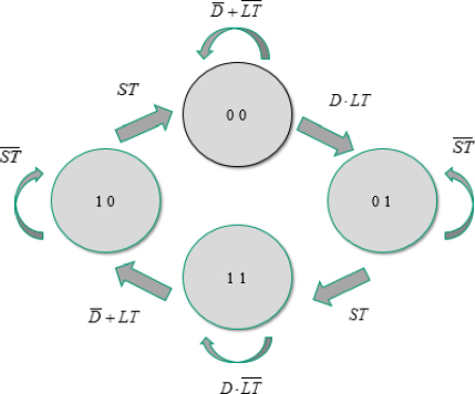
Figure 1.8. Logical diagram of traffic lights
The way in which the lights move from one state to another when the logical conditions have been realized remains to be determined. A solution to this problem consists of using the SET-RESET-type data memory. This function can easily be carried out using classic logic gates. It comprises two inputs and two outputs. When the “SET” input is in the “on” state, the Q output is positioned in the “on” state, or stays in the “on" state if it is already there. When the “RESET” input moves to the “on” state, the Q output moves to the “off” state. The complementary  output takes the complementary values of Q.

Figure 1.9. General diagram customized for the traffic lights model
The two SET–RESET circuits allow us to define the four states identified in the traffic lights model. These outputs are, therefore, the logical outputs of the sequential system. The logical functions command the “SET” and “RESET” inputs, which in this example are the output commands of the data memory identified in the general diagram of Figure 1.6. Figure 1.9 shows the instantiation of the diagram of Figure 1.6 for processing the problem of the traffic lights.
The method for defining the combinational logic necessary for the system consists of filling in the table, which allows it to move from one state to another by indicating the logical conditions, as well as the SET–RESET states. The X symbol indicates that the value of the logical state is indifferent. Table 1.1 is another way of expressing the same as the diagram of Figure 1.8.
Table 1.1. Table of transition between states
| State | Input variables | Next state | Scales | |||||||
| Q1 | Q2 | D | ST | LT | Q1 | Q2 | S1 | R1 | S2 | R2 |
| 0 | 0 | 0 | X | 0 | 0 | 0 | 0 | 0 | 0 | 0 |
| 0 | 0 | 0 | X | 1 | 0 | 0 | 0 | 0 | 0 | 0 |
| 0 | 0 | 1 | X | 0 | 0 | 0 | 0 | 0 | 0 | 0 |
| 0 | 0 | 1 | X | 1 | 0 | 1 | 0 | 0 | 1 | 0 |
| 0 | 1 | X | 0 | X | 0 | 1 | 0 | 0 | 0 | 0 |
| 0 | 1 | X | 1 | X | 1 | 1 | 1 | 0 | 0 | 0 |
| 1 | 1 | 0 | X | 0 | 1 | 0 | 0 | 0 | 0 | 1 |
| 1 | 1 | 0 | X | 1 | 1 | 0 | 0 | 0 | 0 | 1 |
| 1 | 1 | 1 | X | 0 | 1 | 1 | 0 | 0 | 0 | 0 |
| 1 | 1 | 1 | X | 1 | 1 | 0 | 0 | 0 | 0 | 1 |
| 1 | 0 | X | 0 | X | 1 | 0 | 0 | 0 | 0 | 0 |
| 1 | 0 | X | 1 | X | 0 | 0 | 0 | 1 | 0 | 0 |
The logical expressions are deducted from the functions S1, S2, R1, R2, as follows:
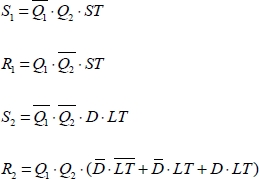
These functions can clearly be carried out by associating them with the AND and OR gates based on the signals available.
This signal is basically an asynchronous system, which means that the signals are not synchronized by an input clock signal; however, in many cases, the clock signal is necessary. The memory circuits are, therefore, synchronized by this signal and the general diagram becomes that shown in Figure 1.10.
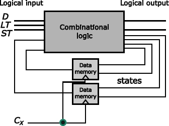
Figure 1.10. Sequential synchronous circuit
To explain the synchronous circuits in more detail, it is first necessary to define memory circuits in a more precise way. A large number of this type of circuits have been created, but we can broadly divide them into two large families: the “latches” and the “flip-flops”.
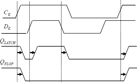
Figure 1.11. Latches and flip-flops
The time-based diagram in Figure 1.11 illustrates how these two circuits function differently. The circuits have two inputs (clock and data) and one output. The output of the “latch” circuit is a simple data copy from when the clock is in the “on” state. It stays in the “off” state when the clock is in the “off” state. It is, therefore, sensitive to the clock level and data transitions. The “flip-flop” circuit is sensitive to the clock transitions (for example, the rising edges) and the output is a data copy. A slight delay is noted between detecting the input signals and the changes in the consecutive output during the signal running time, within the circuits themselves.
These two circuits are frequently used in logic and constitute a “data path” in digital circuits. Before giving a general description of this type of structure, we recall the guiding principle of the “pipeline”-type structure. Let us take a simple example of function computing:

Numbers a and b are binary-coded. The two types of computing architecture are shown in Figure 1.12.
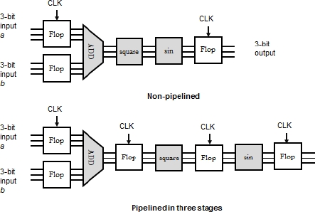
Figure 1.12. Pipelined and non-pipelined architecture types
Let us now consider this circuit’s consecutive data groups, namely a1 b1, a2 b2 and a3 b3, and we will assume that each operator is capable of the computation during a clock period. In order to simplify the problem, let us assume that the delays introduced by the flip-flops are negligible compared to the operator’s computational times, which are all assumed to be equal. Table 1.2 indicates when and from where the operation results are obtained.
Table 1.2. Pipeline functioning
| Clock signal period | Adder (ADD) | Square (square) | Sinus (sin) |
| 1 | a1 + b1 | ||
| 2 | a2 + b2 | (a1 + b1)2 | |
| 3 | a3 + b3 | (a2 + b2)2 | sin(a1 + b1)2 |
| 4 | a4 + b4 | (a3 + b3)2 | sin(a2 + b2)2 |
| 5 | a5 + b5 | (a4 + b4)2 | sin(a3 + b3)2 |
The values are input in clock rhythm. At the completion of five clock periods, the outputs are provided in three pairs of consecutive data. In the non-pipelined version, nothing can be input until the operators have completed the calculations, that is to say three times the clock period. The pipeline gain is, therefore, three.
Sequential pipelined systems are, therefore, used very frequently in electronics. Figure 1.13 shows an example of their general architecture. This will often be used as a structural reference throughout the rest of this work.

Figure 1.13. Sequential pipelined system
We note that the combinational logical outputs are not synchronized, so the delays between the inputs and the outputs depend on how many logic gates it has gone through. The diagram shows that certain logical output signals that are stored can be used in a combinatorial block. Other logical signals can be input externally. The traffic lights model allows us to understand the origins of these signals. The main function of the memory elements is to resynchronize the signals provided by the combinatorial blocks.
1.1.3. NMOS and PMOS transistors
The aim of this section is to give a very simple electrical description of the components that are used today in digital circuits. These components are miniature field-effect transistors whose dimensions are smaller than a micron. They are two different types (NMOS and PMOS) which work together complementarily.
As using an electrical voltage to code a state is the most natural way to continue, the question of asserting a function comes back to establishing the electrical connection between the logic gate’s output in question and a voltage source. This voltage source will need to be set to VDD for the “on” state and zero for the “off” state. Other values can be chosen, such as positive and negative for example; however, for the sake of simplicity, we have chosen to use the two values VDD and zero in the majority of operations. The diagram of Figure 1.14 illustrates how to establish a naturally conducted electrical connection, and to use a voltage-controlled switch.
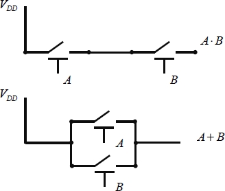
Figure 1.14. Using switches to perform AND and OR functions
Let us assume that a positive voltage, when applied to a control electrode, turns the switch on and establishes the connection while a voltage of zero holds the switch open. Historically, the first logic gates were carried out using electromechanical switches in the 1930s. The need for miniaturization led to replacing this technology with that of vacuum tubes, which was then replaced by semiconductor-based technology from the 1950s onwards. It is only very recently that researchers have again begun to experiment with technology based on electro-mechanic relays, but this time in a miniature version. This option will be studied in more detail in Chapter 8.
The diagram of Figure 1.14 shows how the first logic event provides a “1” state as an output and works perfectly, but it cannot accept a second event. It is necessary to understand how the input logical states are configured for each event. In fact, let us start with a configuration in which the output is at a voltage of VDD. When the input voltage values change to zero, the output voltage either remains in the “on” state or evolves indefinitely depending on the gate’s electric charge. Therefore, it is necessary to predict how many inputs will electrically reset it to zero. This then leads us to the diagram shown in Figure 1.15. A second relay set allows us to connect the output to zero potential when the function is not asserted, wich is to say when the complementary function is.
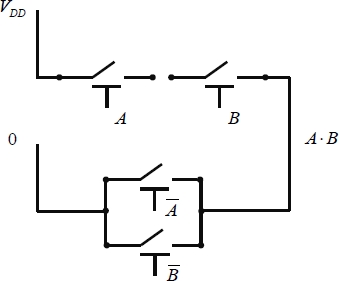
Figure 1.15. The complete AND function
Note that it is necessary to have the input’s logical complements at the ready, such as the complement A · B as  . This logic is called complementary logic and the general diagram explaining it is shown in Figure 1.16.

Figure 1.16. Complementary logic
When using complementary metal oxide semiconductor (CMOS) technology, performing logic gates in complementary logic becomes much more simple. This is because the complementary function that is connected to the zero potential, generally the circuit ground, can easily be obtained from the signals rather than from the complements. Moreover, it excludes all permanent conducting paths between the supply voltage and the ground, which, in principle, should reduce electrical consumption to zero. The remainder of this book will show that due to dynamic consumption and current leakage, this is not always the case.
Thanks to some very simple elements, we can easily describe CMOS technology based on two miniature switches: the NMOS transistor and the PMOS transistor. This will be described in more detail in Chapter 3.
Figure 1.17 describes very simply how NMOS and PMOS transistors work. These silicon-based devices allow a current to circulate between the input and the output called the source and the drain, depending on the tension applied to an isolated electrode in the conductive area called the gate. This gate is separated from the silicon conductive area by a very thin (approximately 1 nm) layer of oxide, which enables a powerful electrostatic effect. The diagram describes the two components by indicating the direction of the conventional conductive current, meaning that in which the positive charges go from the highest potential to the lowest potential. Note that the definitions of source and drain are interchangeable as the device is symmetrical. The same physical electrode can be the source or the drain depending on the direction in which the current is passing through the transistor.

Figure 1.17. NMOS and PMOS transistors
In the case of PMOS transistors, where the holes ensure the conduction, the conventional current has the same sign as the physical current. Moreover, as would be imagined from the definition of the terms drain and source, the currents circulate from the source to the drain. The condition to be fulfilled is that the voltage difference between the source and the gate must be greater than a positive value called the voltage threshold:

In fact, as will be discussed in Chapter 3, the voltage threshold of PMOS transistors is negative, but it is simpler to reason using positive values, voltages or currents and then to take the absolute value of the voltage threshold.
In the case of NMOS transistors, the conventional current circulates from the most positive voltage to the least positive voltage, but as the conduction is ensured by the electrons, the physical current goes in the opposite direction. This explains how the drain and the source are permutated as the physical current always circulates from the source to the drain. The condition to be fulfilled is that the voltage between the gate and the source must be greater than a positive voltage called the voltage threshold:

Note that the condition is based on the difference between the gate voltage and the source voltage, rather than between the source voltage and the gate voltage, as was the case for PMOS transistors. Those readers who are not very familiar with CMOS technology will no doubt need to spend some time mastering how to check the signs and how to localize the source and drain electrodes, using the diagram indicated in Figure 1.17, if need be.
We can now study the NAND gate, the inverse of the AND gate, and we will represent the diagram for it using PMOS and NMOS transistors. The equivalent diagram based on switches is shown when the two inputs are at “0”. Therefore, the NMOS transistors are open and the PMOS transistors are closed. In Figure 1.16, we recognize the logic blocks and their identified complements. What is unique about CMOS technology is that it is not necessary to have complementary states.

The function used in this example is a logical NAND, as it is one of the simplest gates to perform. It would have been possible to choose the inverter function as many other authors have chosen to do, but it is perhaps more convincing to use a multiple input function in this instance.
Furthermore, the inverter will often be chosen as an example as it is only composed of two transistors and also because its structure is the base structure for all logical functions. The AND function could have also been chosen here, but it is slightly more complex to design. The logical functioning of complementary logic can be explained by switch-based performance. It does, however, add new complexity that CMOS logic does not have. In fact, in CMOS technology, the two types of transistors work in a complementary way in the physical sense of the term and it is not necessary to have the complements of each input.
When the two inputs are in the “on” state, the two NMOS transistors are conductive as the gate-source voltages equal to VDD are greater than VTN. The output voltage is, therefore, zero. The PMOS transistors are blocked, which means that no continuous current can circulate between the supply voltage and the ground. When one of the inputs is in the “on” state and the other is at zero, the conduction path given by the NMOS transistor is open but the PMOS transistor is a conductive. The output voltage is then slightly different from VDD. Finally, when the two inputs are at zero, the two PMOS transistors are conductive and the NMOS transistors are non-conductive, thus placing the output voltage at VDD. When the states change, the transients circulate, yet only for charging and discharging the capacitors that are not shown in the diagram, but which are nevertheless present. These are not only input capacitors of the next stages, but also the equivalent output capacitors and similarly the equivalent interconnect capacitors.
1.1.4. Complementary CMOS logic
While the general principles have already been introduced to explain how this logic functions mainly in digital circuits, it is still useful to outline some of the general properties.
1.1.4.1. Propagation time and how to minimize it
This parameter measures the delay between the input and the output in a logic gate. For many years, this has been absolutely crucial, as the main objective has been to increase the speed at which digital circuits ran. Nowadays, this objective remains important, but there is also another constraint to grapple with: expending the least amount of energy. This new objective was broadly explained in the introduction. Circuit designers are thus faced with problems in balancing between obtaining a faster speed and controlling heat dissipation.
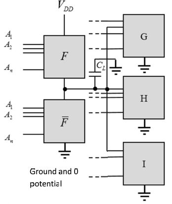
Figure 1.19. CMOS circuit and output capacitor
Figure 1.19 shows a CMOS gate in its own environment, as it can command a rather large number of other gates. This number is the gate’s “fan-out”. Electrically speaking, the output is not only equivalent to the input capacitances of the connected gates. Interconnect capacitances have also to be included. The average value of a linear capacitor for a copper or aluminum line is 2 pF by centimeter length. This value is generally the same regardless of which technology has been chosen or which level of interconnect is considered. We will assume that the equivalent input resistances for related gates are very high. The total for standard technologies with a CL capacitor is approximately 1 fF. This capacitor plays a major role in the estimation of both the propagation time of the gate and the heat dissipation. This last point will be studied in further detail in section 1.2 of this chapter.
To complete the concept diagram of the NAND gate (Figure 1.20), we use a simple but effective diagram. Each transistor is represented by an ideal series switch with a resistance that represents the conduction channel resistance of the component. Values around 10 kΩ are very large, but dependent on the technology and transistor size. This diagram raises new questions for the dynamic functioning of CMOS gates. It also allows us to understand the nature of the balance to be obtained between choosing a faster speed performance and achieving a smaller energy expenditure.
Starting with a state at which the two inputs are at the “1” state, the two NMOS transistors are conductive, the two PMOS transistors are non-conductive and the output is close to “0”. When one of the inputs (A for example) moves into the “0” state, the conduction path is cut between the output and the ground. However, one of the PMOS paths is conductive, which allows the CL capacitor to be charged until it attains a voltage close to VDD at its terminals. The time constant associated with this charging is the product RPCL. In the next section, we will see how the dissipation in the resistance RP is 1/2 ∙ CL ∙ VDD2 and is therefore independent of RP. This may come as a surprise, but it will be very thoroughly demonstrated.
If the output A now returns to “1”, the conducting path between the supply and the output will again become broken, but a conducting path now appears between the output and the ground as one of the NMOS transistors is conductive. This allows the ground capacitor to discharge through the two Rn resistances. It can be deduced, therefore, that the switching time is approximately 0.7 · RPCL for one transition and 1.4 ∙ RnCL for the other.

Figure 1.20. Simplified electric diagram of a CMOS gate
These times can vary according to the logical configurations and the number of inputs (fan-in). To give an example of scale, 10 ps for an advanced technology correspond to a capacitor of 1 fF and a resistance of 10 kΩ. These scales indicate that the switching speed is no longer really an issue in CMOS technology. The resistance of a transistor at conductive state is weak when the width of the transistor is important, in comparison to the length of the conduction channel. These aspects will be discussed in detail in Chapter 3.
1.1.4.2. Activity factor and how to reduce it
If we admit that each transition in a gate, or a changing of output state, leads to dissipated energy amount of 1/2 ∙ CL ∙ VDD2 and if we use α to represent the probability that this transition takes place during a given time period T, the average dissipated power is then:
When f is the circuit function frequency (the clock frequency in Figure 1.13), the relationship that gives rise to the gate’s dissipated power is written classically as:
The activity factor of a logic gate is therefore a determining aspect for the level of power dissipation.
Let us take the example of a NOR gate with two inputs (A and B). If pa and pb are the probabilities that the two inputs will be at “1”, and assuming that the inputs are independent, the probability that the output will be at 1 is therefore:

The gate’s transition probability (changing from 0 to 1) is thus:

In the same way, the activity factors of AND and OR can be found. The results are summarized in Table 1.3.
Table 1.3. Activity factor for the common gates
| Gate | Activity factor |
| AND | [1 − papb] papb |
| OR | [1 − (1 − pa) (1 − pb)] · [(1 − pa) (1 − pa)] |
| NOR | [1 − (1 − pa) (1 − pb)] · [(1 − pa) (1 − pa)] |
| NAND | [1 − papb] papb |
| XOR | [1 − (pa + pB − 2papb] · [pa + pB − 2papb] |
These results allow for optimized organization of the gates in a complex function, so as to reduce the activity and dissipation rates. This can be done by changing the input order, or rather changing the way in which the gates cascade.
1.1.5. Pass-transistor logic
This logic is used a lot less frequently than CMOS, but it has the advantage of reducing the number of transistors, by synthesizing a given function. Moreover, certain aspects of it are taken up in adiabatic solutions. Figure 1.21 shows an AND gate using this technology.
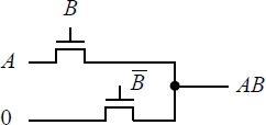
Figure 1.21. AND gate in pass-transistor technology
When the two signals A and B are at VDD, the high transistor above is a conductive and the voltage VDD is in output. When the signal B is at 0 and A at VDD, the lower transistor is a conductive and the output is zero. When the two signals A and B are at zero, the lower transistor is a conductive and the output is zero. Note that it is necessary to have an inversion for the signal B, and that four transistors are therefore necessary, as opposed to the six transistors needed in CMOS.
This technology has a major drawback. When the output node is on, as in the case when the higher transistor conductive, the output voltage cannot go beyond VDD – VTn because the gate–source voltage cannot be less than the threshold voltage in conduction. This voltage loss accumulates when many gates are cascaded, it leads to a function loss. Therefore, CMOS inverters will need to be added in order to restore the appropriate electrical levels.
In general, circuit designers use an improved version of this logic in the form of a differential logic, which means making use of the signals and their complements. Figure 1.22 describes the basic gates when using this technology.
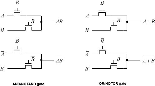
Figure 1.22. Differential pass-transistor logic
With the node always being electrically associated with VDD or zero across a relatively low impedance, the noise immunity is good. All the gates have the same topology, which makes the layout easier. However, this technology has the same drawback as the basic pass-transistor technology: the high output is less than VDD, which poses a problem in the gate series and induces static consumption. A recent improvement made to correct this defect gave birth to Pass-Gate technology. NMOS transistors are good at transmitting 0 V, but poor at transmitting VDD voltage (VTn deficit). PMOS transistors, on the other hand, are poor at transmitting 0 V, but good at transmitting VDD voltage. It is, therefore, interesting to draw a parallel between the two as a switch.
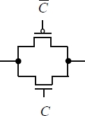
Figure 1.23. Transmission gate
This device, shown in Figure 1.23, is called a transmission gate and is commanded by two signals, the signal and the complement. This technology will serve as the basis for the low-consumption solutions to be studied in Chapter 7.
Figure 1.24 illustrates the properties of the transmission gate in the two different cases: transmitting the voltage VDD at the output (initially zero) and the output’s discharge (initially VDD) at the ground.

Figure 1.24. Transmission gate functioning
In the charge operation for the output capacitor, NMOS transistor is the conductive as long as the gate-source is greater than the voltage threshold. The PMOS transistor then takes over at the end of the charge. In the discharge operation, the PMOS transistor is the conductive and then the NMOS transistor takes over at the end of the discharge. In both cases, the operation has been performed in its entirety. This logic allows us to easily implement all of the logical functions. The exclusive OR gate, is used as an example in Figure 1.25.
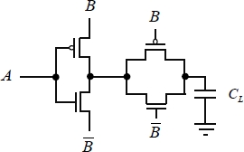
Figure 1.25. Exclusive OR in Pass-Gate logic
1.1.6. Dynamic logic
Dynamic logic was also originally proposed to reduce the number of transistors and to increase the speed. It is used to carry out high-performance functions, but it is more difficult to implement than classic CMOS, which limits the scope of its application.
In contrast to the technologies already presented in the earlier sections, the logical states are performed in a fraction of the functioning time, and not on an ongoing basis. Two phases are defined here: a pre-charge phase and an evaluation phase. These two phases are selected according to a clock signal that synchronizes the logical operations.
When the clock is at “0”, the gate’s output signal is positioned at VDD. When the clock is at “1”, the output is then conditioned by the input states and the gate is in the evaluation phase. When the function is being performed, a conduction path is created toward the ground, as in this case the NMOS transistor at the bottom of the diagram is conductive. Figure 1.26 depicts a NAND function with two entries being performed.
Note that in every case, no conduction path is possible between the supply and the ground Furthermore, in contrast to CMOS, no intermediate regime can take place with a partial conduction of the two NMOS and PMOS transistors at the same time. In principle, a single changing input state can be taken into account during a clock period.

Figure 1.26. NAND function in dynamic logic
It is also worth noting that the output’s electrical node is floating during the evaluation period. With the connected gates’ inputs being at a high impedance, the output potential remains the same throughout the period, on the condition that the inputs do not change. In practice, the potential can decrease under the effect of transistors’ current leakage. However, as long as the clock period is not too long, this decrease is negligible. It is from this property that the name of this logic (dynamic) originates.
This logic has two important advantages:
- 1) A limited number of gates to perform a logical function. While CMOS uses 2N transistors, dynamic logic uses approximately N transistors. This advantage translates into a lower footprint and a lower switch capacitance.
- 2) A faster speed than CMOS, as the capacitances are decreased by the reduction in transistor numbers.
On the other hand, the sensitivity of the floating node to electromagnetic interferences is more significant than in classical CMOS. In particular, the clock signals can interfere with this logic’s functioning when the layout is not carried out carefully. This inconvenience should not be considered as a minor one, as it is the real drawback to the generalization of this logic, which otherwise offers significant advantages.
The general diagram of a gate in dynamic logic is depicted in Figure 1.27.
Dynamic logic also presents some further difficulties, which we will not discuss in this introduction. There is only one worth commenting on as it is the source of the more popular version of dynamic logic, namely Domino logic.
It is impossible to directly cascade two gates similar to those shown in Figure 1.27. We will use the example of the two inverters depicted in Figure 1.28.
When the clock is in the “on” state (evaluation phase), a positive input brings about the ground discharge of the first gate’s output voltage. The output voltage of the second gate also discharges as NMOS transistor T2 is also a conductor, due to the fact that the output voltage of the first gate is greater than the threshold VTn. When the output voltage of the first gate is less than the threshold, the conduction path toward the ground is interrupted and the output voltage of the second gate is blocked to this value because the output node is insulated. This intermediate value between 0 and VDD is not authorized in dynamic logic. A solution to this problem is to insert a classical CMOS inverter in between the dynamic gates as is depicted in Figure 1.29.
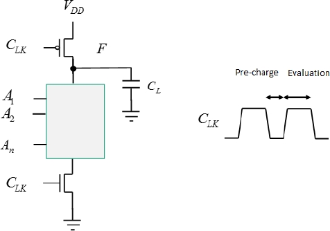
Figure 1.27. Dynamic logic gate
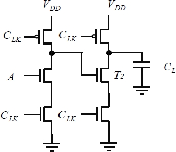
Figure 1.28. A diagram that is not functional
In order to conclude this introduction, we must remember that the majority of digital functions have been designed and based on the classical CMOS structure, whose reliability and sturdiness have been proven. It is very resistant to the electrical parameter variations and its noise immunity (induced interfering signals) is excellent. The most original, but very delicate dynamic and Pass-Gate solutions which will be focused on, do however have points in common with the very low-consumption circuits These will be further detailed in Chapter 7 of this book.
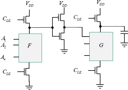
Figure 1.29. DOMINO logic
1.2. Origins of heat dissipation in circuits
1.2.1. Joule effect in circuits
In this short section, we will identify and analyze the main causes of heat dissipation. The physical origins of thermal dissipation will only be dealt with in summary, as they are based on rather complex models that are detailed in solid-state physics [ASH 76].
The law that is generally applied is Joule’s law, which links dissipation to the current flowing through resistance. Dissipated power, which is to say energy transformed into heat by time units, is written in the classical way:
In this relationship, R is the resistance in question and I(t) is the value of the instantaneous current assumed to be flowing through the device. As the difference in potential at the terminal is U = RI, it can also be written in the following form:
This relationship is more general and tends to be applied to devices where Ohm’s law is not valid, such as metal–semiconductor junctions or semiconductor–semiconductor junctions. This relationship can be explained quite simply when we consider a device with two ports, one input and one output, as shown in Figure 1.30.
The negative charges NA that manage to cross over the electrode-device barrier in A by time units give the device a potential energy of  . On the other hand, the NB charges that manage to cross over the electrode-device barrier withdraws an energy of
  from the device. The energy variation of the device is, therefore,
  . Conserving the current allows us to write that NA and NB are equal in this type of geometry. The potential energy variation is, therefore,
  . If we now assume that the sum of the considered carriers’ kinetic energy has not changed (as it depends only on the assumed homogenous temperature in the device), we can confirm that the potential energy variation must be accompanied by heat production. This heat is the result of interactions between mobile charges and the device’s atoms that vibrate more or less.

Figure 1.30. Dissipation in a two-port device
In reality, the physics of this phenomenon is described in a much more complex way when it is modeled on wave function interactions representing the carriers with the atom network’s vibration field. This result can be applied not only to pure or intrinsic resistances, but also to devices of the following types: metal–semiconductor; metal–metal; semiconductor–semiconductor and intrinsic semiconductor. In a perfect insulator, the current as well as the dissipation will be assumed to be null.
Let us now take the example of a series resistance with a metallic or semiconductor component, and a capacitor similar to that shown in Figure 1.31. There is no heat dissipation in the capacitor. In fact, assuming that the capacitor is ideal, all of the energy variation corresponding to the influx of negative charges to an electrode and the influx of positive charges to the other electrode will fully convert into stored energy variation in the capacitor. This energy is brought about by the following relationship:
The voltage VC is the voltage at the capacitor’s terminals.

Figure 1.31. RC circuit and heat dissipation
1.2.2. Calculating dynamic power
The two elements are connected to a voltage generator, which itself is connected to the ground. The source of this generator’s output voltage may be attributed to different origins: chemical, mechanical or electrical. A similar reasoning to that given in the introduction shows that the power delivered by this generator is  . In order to simplify the problem, let us assume that the voltage form is an applied procedure starting at 0 to attain a value of VDD. Then, we calculate the voltage at the capacitor’s terminals. The system is figured out with a very simple differential equation:

Initially, the voltage at the capacitor’s terminals, as well as the electrode’s charges, is null. The equations can be summarized by a single pair of relations:

This initial condition is a consequence of the capacitors’ law; starting from 0, another voltage value immediately after applying the generator voltage would lead to an infinite current, which is physically impossible. This system’s conclusion leads to the well-known relationship:

The voltage at the capacitor’s terminals starts from the value of 0 and moves toward the value VDD following an exponential law of time constants RC. From this, we deduct the value of the current in resistance, and then the value of dissipated energy in resistance throughout the infinite duration of the capacitor’s charge:

Calculating this integral allows us to obtain the well-known value:
Therefore, dissipated energy does not depend on the resistance value, but on the capacitance value. This value is equal to the energy stored in the capacitor at the end of charging, which is in theory at the end of an infinite time. Both of these results may come as a surprise, but nevertheless, they remain to be true if the resistance varies with the terminal voltage. This case concurs with a capacitor through a transistor.
A simple energy calculation is enough to demonstrate this. A constant voltage A is provided by the generator (this precision here is absolutely important), and the energy delivered by the generator to charge a capacitor through any resistive network is given by:

As the voltage is constant:

The Q charge is that delivered by the generator. After charging, it is fully stored in the capacitor, in line with the charge conservation principle. If the system is composed of various capacitors, it is divided according to the capacitor values. The stored energy is thus:

or

So, half of the provided energy is dissipated into heat.
The result is identical for the case of various capacitors. In a logic gate, the output capacitor is charged when the output moves to the “on” state (“1”), which corresponds to the probability α that we have already defined as being the activity rate. In order to define the activity rate, we generally choose the time period as the inverse of the circuit clock frequency. Having chosen this period, the dissipated power per logic gate is then:
1.2.3. Calculating static power and its origins
To conclude, we will give a few points on static consumption. In a circuit containing a conduction path between the supply line and the ground, a continuous current circulates in permanence and generates a rather irritating dissipation, as it does not connect with any logical operation. This situation should be avoided at all costs and very thankfully, the problem can be resolved by complementary and dynamic logic. However, we need to do this while taking account of the threshold current in semiconductor-based technology. Transistors, even cut-off ones, meaning those that are controlled below the threshold, do not have a strong enough resistance value and so a current called a sub-threshold current circulates. This residual current can be written more precisely as:
In this expression, VT is the voltage threshold that corresponds to the chosen technology. The values are different for both NMOS and PMOS transistors and values of 300 mV are the usual ones for current technologies. The exponential dependence of the sub-threshold current shows how acutely sensitive static dissipation is to the choice of threshold voltage.
This phenomenon is aggravated by the effects of variability. When the transistor size diminishes, the threshold voltage’s static dispersions increase. This happens even though a non-negligible amount of transistors may have threshold voltages that are far less than the average value, and significantly contribute to an increase in the sub-threshold current. This is a major difficulty in CMOS technology and explains how many current technologies and architectures have evolved the way they have.
The fundamental problems faced by physicians and circuit designers are how to restrict threshold currents and the variation in average values for threshold voltages. Increasing the average value of the threshold voltage is not a viable solution in this case because, as explained in the previous section, the supply voltage and the dynamic power would also need to be increased. Breakthrough technologies may be invented to radically deal with this problem by designing non-semiconductor devices with negligible current leakage. In Chapter 8, we will further provide the example of electro-mechanical nano-relay technologies.
In the case of extremely miniature devices, another detrimental physical phenomenon appears – the tunnel effect. This typically quantic effect shows that a current can circulate between two electrodes separated by a very weak insulating layer. The typical width is in nanometers. The wave function associated with the carriers can actually extend beyond this dimension and a current can circulate when affected by a relatively weak potential difference, such as the potential difference between the gate and the semiconductor. Controlling the tunnel effect between the gate and the conduction channel has led to restricting how much the oxide’s width can be decreased. It has also led to using high-permittivity materials to obtain an equivalent electrostatic effect.
Furthermore, a tunnel effect can occur between the source and the drain independently of the grid voltage value. The transistor functioning is therefore severely impaired. This effect is not a restriction today but it could become so if miniature devices begin to have channel lengths of less than 5 nm.


