4
Practical and Theoretical Limits of CMOS Technology
CMOS technology has made considerable progress in the realms of reducing transistor size since the 1960s. The cost of electronic function has fallen by 10-fold, and operating frequencies have continued to increase right up to the 2000s. The evolution of this technology has, however, collided with a major setback: the rise in dissipated power. There are two main reasons for this: the impossibility of reducing the voltage much lower than the volt level and the surge in sub-threshold currents. It has, therefore, been necessary to stabilize the operating frequency at a maximum of a few gigahertz. Nevertheless, the number of components per surface units has not ceased to grow. The trend of miniaturization has not progressed as fast as predicted, but it still remains at the heart of advanced micro-electronics. In this chapter, we will analyze the causes for this significant problem and lay out the possible paths of recourse. The sub-threshold regime will be specifically analyzed. The last section attempts to set out the clearest possible aspects to identify the potential theoretical limits, which remain to be the subject of conflicting debates.
4.1. Speed–dissipation trade-off and limits of CMOS technology
4.1.1. From the transistor to the integrated circuit
An integrated digital circuit is made up of a set of interconnected logic gates. Currently, the amount of gates may reach the millions. Chapter 1 showed that all gates were based on the inverter pattern carrying a PMOS series with an NMOS. Manufacturing small transistors is easy. It is not the same for the other components in electronics: resistances, capacitors and inductances. It is very difficult to obtain high values for resistances, capacitances and inductances. Therefore, electronic models are designed to use these components as little as possible.
Figure 4.1 shows two integrated circuits: the first ever integrated circuit built in 1961 and a 2000-era processor. Although the amount of transistors has largely increased, the chip size has stayed at around cm2 for complex circuits.

Figure 4.1. Integrated circuits
The inverter-based model, as well as its physical layout, is represented in Figure 4.2.
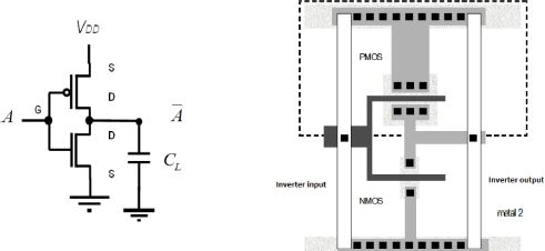
Figure 4.2. Inverter model and layout
Figure 4.3 shows a sectional view of the inverter in classic CMOS technology. We note the presence of a doped well n, which enables the PMOS transistor, insulation trenches and interconnections to be carried out. In reality, the current integrated circuits may contain various interconnect layers.

Figure 4.3. Sectional view of the inverter
The interconnect plays a major role in the operating of integrated circuits, especially in regards to the dissipation properties. They are in fact electrically equivalent to capacitors. Energy properties that depend on charge capacitance are actually also directly dependent on interconnects. The interconnect dimensions vary according to their position in the particular layer in question.
Interconnects that link the close transistors (levels 1 and 2) have weak width and length. The interconnect that corresponds to data lines (data “buses”) is much longer, wider and thicker. The same can be said of supply lines and those aiming to carry out ground planes. However, the equivalent capacitance in each case is in the order of magnitude of 2 pF/cm. Figure 4.4 may help us to understand this property, which will be very useful when estimating energy performances. The equivalent resistances per interconnects’ unit length, on the other hand, depend on the level of the layer.
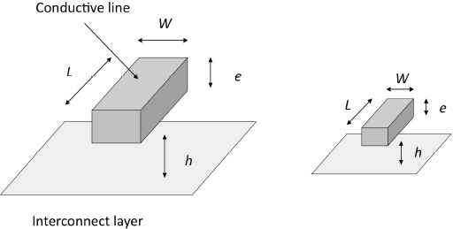
Figure 4.4. Interconnect and scaling
The interconnect’s resistance is written in the first order:
When moving up to a more advanced technological node, the dimensions become: αW, αh, αe.
The capacitances and resistances become:
The capacitance per unit length only varies a little, but the resistance per unit length increases with miniaturization. This analysis is just an overview as it does not account for coupling capacitances with other interconnect lines, but instead just explains the results of the first order.
4.1.2. Trade-off between speed and consumption
The link between circuit speed and electrical consumption is well known in electronics and any increase in the operating frequency is paid for by an increase in consumption and heat dissipation. Speed and dissipation are, however, two distinct entities and, in theory, it is possible to have a high-voltage electronic functioning, which recovers the energy lost in computing operations. The adiabatic solutions introduced in Chapter 2 are heading in this direction. In practice, the logical operations associated with dissipation depend on the capacitance value and supply voltage, as shown in Chapter 2. The results given in Chapter 3 allow us to make the general notions more specific to the case of CMOS technology.
A first analysis of the problem consists of considering that the maximum switching frequency of the inverter stage is given by the time necessary to charge the capacity capacitance CL in Figure 4.2. This includes not only the capacitance of all the interconnects at the gate’s output, but also the input capacities of the connected gates and the output capacitance of the gate in question. In the first step, the capacitance is charged by the PMOS saturation current, and it can be written as:

Assuming that the current remains constant throughout the charge period, which is actually a rough estimate, we obtain the necessary time for switching:

or

The dissipated energy is:
The product of dissipated energy and the switching time can be considered as a figure of merit to be optimized, if equal importance is given to both speed and consumption. Other figures of merit may be defined, such as Δt ⋅ E2 or Δt2 ⋅ E. The simple product is that which is mostly used in practice. Minimizing this product leads to the derivation of the following equation:

From this, it can be deduced that the supply voltage value is approximately three times the value of the threshold voltage. This rule is often used empirically and can be explained by a very simple analysis. This calculation glosses over the sub-threshold current. The simplification was justified for older CMOS technologies, but it is no longer justified in the use of current CMOS technologies.
The result obtained also indicates the effect of the transistor’s size. This is for a transistor in which the ratio W/L is weak and incompatible with higher operating frequencies. This observation explains the trade-off that has to be made between choosing a very fast speed and the size of the logic gate, so its cost.
The previous calculation only took into account the PMOS inverter properties. The reader may quite rightly wonder what the use of this analysis is if it ignores half of the circuit’s components. In reality, as has been studied in Chapter 1, after a transition from the “off” state to the “on” state, the reverse transition is possible: to go from the “on” state to the “off” state. In this case, the capacitor CL discharges at the ground through the NMOS transistor. In the same way, the dissipated energy is 1/2⋅CLVDD2. The discharge time is in the same order of magnitude as the charging circuit with a slight difference being that the mobility of the NMOS electrons is higher than that of the PMOS holes. Optimizing the figure of merit leads to the same rule.
Specific analysis of the inverter shows that it is useful to choose the PMOS width at about three times that of the NMOS. This choice enables the logic gate’s threshold voltage to be half the supply voltage, which ensures a good level of noise immunity. Note that the gate’s threshold voltage, meaning the voltage from where the gate switches is different from the transistor’s threshold voltage. To prove this, you only need to assume that the PMOS and NMOS transistors are in the saturation regime, and to write their values as equal when the states change:

In this equation, V is the input voltage applied on the two gates. V can thus be calculated:
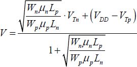
If this value is VDD/2, assuming that the threshold voltages are equal, the below equation is obtained:
4.1.3. The trade-off between dynamic consumption and static consumption
The following calculation is very important, because it shows that CMOS technology is limited when it comes to energy properties. It is based on a very general model and on the results obtained in Chapter 3. Although this is a crucial approach, it is not very well known in the literature. The basic layout is that of the inverter, just as in the majority of these cases already dealt with. The results transpose very easily to more complex logic gates (AND, OR, NAND, NOR, etc.) as explained in Chapter 1.
This calculation looks at the gate’s passage from the “off” state to the “on” state. The output capacitance CL is charged at the voltage VDD. During the time accounted for, such as the clock period, a sub-threshold current also passes through the NMOS. Choosing the clock period will guarantee that only one logical transition is possible during this period. To understand this, we only need to refer back to the sequential logical architecture. At the time of logical transition, the two inverter transistors can simultaneously be both conductors for a brief time. The associated dissipation is weak though and will not be taken into account in this calculation. In summary, two terms will be taken into account: the PMOS charge current and the sub-threshold current passing through the NMOS during the period T considered.
Dynamic consumption is simply  , an expression in which a is the gate’s activity factor and expresses the probability that a logic transition will take place during the set period. This value can vary widely according to the logic operator in question. In the pipeline of a calculating operator, values between 0.1 and 1 are possible. In address decoders, rates that are much weaker are frequent.
Static consumption is not only due to the sub-threshold current when the NMOS is blocked after transition, but also due to the PMOS sub-threshold current before transition. To somewhat simplify this, we can consider that these two currents are approximately the same. During the period T, the same current circulates between the supply and the ground, creating thermal dissipation equal to:

The values VGS or VSG are in fact zero both before and after transition. The values VDS or VSD are close to VDD . The value I0 depends on the chosen model for the sub-threshold current. In the first step, we will neglect the short-channel effects and the DIBL. The parameters to be optimized are the threshold voltage and the supply voltage, assuming that the activity factor as well as the period T are given. We will also assume that the speed constraints impose a minimal relationship between the supply voltage and the threshold voltage:

Conforming to the factor of merit in the previous section, we will choose k equal to three. Although we keep the factor k here as a parameter that is adjustable according to its application, we can still determine the speed constraints. The total dissipated energy is:

We put
And the dissipated energy becomes:

Neglecting the term e−kn0y when the unit is present, we obtain:

This factor m depends on some technological factors, such as (I0, n0), and also on architectural parameters (a, T, k). The vast majority of digital applications given bring about values between 10 and 1,000. For example, it is equal to 70 for CMOS technologies of 45 nm and a standard inverter. The transistor size is included in the term I0. Studying the function f (y) = y2 + mye−y allows us to easily find the optimum, as shown in Figure 4.5.
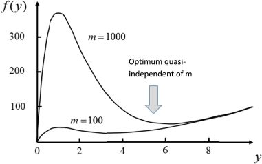
Figure 4.5. Characteristic function of dissipation in CMOS technology
This curve is very generic and, therefore, fundamental. The case (m = 1,000) corresponding to very advanced technologies shows clearly that there is an optimum threshold voltage of y near 6, which corresponds to an optimal threshold value:

With n0 = 1.3, a typical value in CMOS, we obtain:

While this value is quite close to the values effectively chosen in the applications, it is weaker. This difference can be explained by taking DIBL into account.
For the weaker values of m (due to older technologies or bigger transistor sizes), the minimum is less marked. When there is a kind of plateau, it is worth choosing the value y and the highest possible threshold. Then we need to choose the ratio between the supply voltage and the threshold voltage according to the operating frequency. The switching time is given by the below equation:

As choosing the highest possible value for the threshold voltage guarantees that the dissipated energy does not increase much, the switching time can be minimized while the dissipation is also limited.
Let us now introduce the short-channel effects. The dissipation becomes:

Now defining y by:
we can easily obtain:
The optimal value of y is the same but the threshold voltage and the dissipation increase. For high values of m, we obtain an optimal value of y that is equal to 6:
For advanced technologies, we obtain optimal values of approximately 300–400 mV.
As the equation gives the dissipated energy’s value to be optimum through transition, the ratio between static energy and dynamic energy can also be easily determined according to the parameter m. Two values are calculated in Table 4.1.
Table 4.1. Static energy and dynamic energy
| Parameter m | Optimal parameter y | Dynamic energy | Static energy | ratio |
| 100 | 4 | 16 | 7.3 | 45% |
| 500 | 5.5 | 30 | 11 | 36% |
4.2. Sub-threshold regimes
4.2.1. Recall of the weak inversion properties
Contrary to the widespread idea, it is possible to make logic gates operate using a supply voltage that is weaker than the transistor thresholds in CMOS technology. To charge a circuit’s electrical capacitors, the logic circuit needs only two easily differentiated states and a minimum current. However, if the operating frequency is low, the currents may be weak. The electronic circuits used in watches and certain circuits aimed at autonomous sensors make use of the sub-threshold electronics. The transistors operate on a weak inversion regime. This regime was discussed in extensive detail in Chapter 3, but it may be useful to recall its main properties. In the sub-threshold regime, the NMOS drain current can be written as:
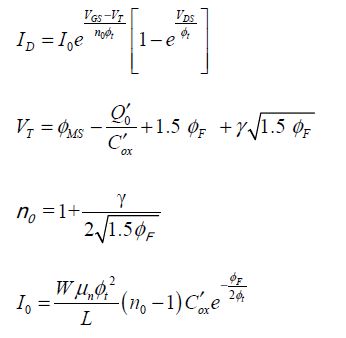
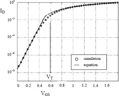
Figure 4.6. Current in weak inversion
All the quantities are described in Chapter 3. Remember that W and L are the width and length of the channel, respectively, ϕF is the Fermi potential of the doped semiconductor p,  is the capacitance per surface unit of the insulated gate, ϕt is kBT/e and γ is the coefficient that represents the “body” effect. Therefore, this current has an exponential dependence on the applied input voltage between the gate and the source, and the input capacitance is shown to vary quite significantly when going from the sub-threshold regime to the normal regime. The curve shown in Figure 4.6 compares a simple model with specific simulations.
4.2.1.1. Calculating and minimizing dissipated energy
The following results are based on an article published in 2005 by Calhoun and Chandrakasan [CAL 05]. The aim is to calculate the average dissipation in a logic gate operating below the threshold and to determine the optimum conditions for polarization. The analysis is not limited to an inverter, but instead can be extended to any logic gate. Figure 4.7 symbolizes a NAND gate and can serve as an example.
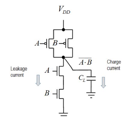
Figure 4.7. Example of a logic gate
Here, we will study this gate’s operation over the time T corresponding to a system clock period. Remember that, in a logical structure, a certain amount of combinational gates are put into a series between two registers. During this time, there is only one possible state change for any given gate. The probability that there is a change is symbolized by a and is called an activity factor. There are multiple propagation paths possible between the two registers, but the longest path as measured by the maximum amount of gates it has possibly passed through is called the logic depth LDP .

Let us now come back to a logic gate in a global architecture, using the NAND example. When the voltages A and B are in the “on” state, near VDD, the PMOS are cut and the NMOS are conductive. The output is in the “off” state and the voltage is close to zero. A leakage current is now circulating in permanence, the sub-threshold PMOS current when the gate voltage is close to VDD. When the two outputs move to zero simultaneously, the two PMOS become conductors and the output capacitor charges while creating a dynamic dissipation. The two NMOS are then blocked and a leakage current circulates in permanence, as determined by the NMOS sub-threshold regime when the gate–source is at absolute zero.
For other gates, there may be various PMOS in parallel and the permanent leakage current would be more significant. Generally, the leakage current that is circulating in the gate can be calculated by taking the same value for the two threshold voltages (PMOS and NMOS) and by introducing a dimensionless coefficient Weff translating the fact that multiple transistors may interfere.
The calculation is based on the general valid formula for a typical length transistor, given at the beginning of section 2.1, by making VGS equal to zero:

The minimal period T is also equal to LDPtd, the relation in which both the logic depth and the delay introduced by a gate are recognized. This delay is estimated based on the output capacitor charging time. The charge is assumed to be a constant current. This current is provided in the example by the two PMOS in parallel. This estimate brings us to introducing the correction coefficient K. The amount of transistors in parallel occurring in the charge corresponds to the parameter nt:

Now, we write the dissipation occurring during the period T. In order to calculate the leakage current, consider the gate–source voltage to be at absolute zero. To calculate the dynamic consumption, the activity factor a will need to be integrated:

By replacing I0 with its value pulled from the charge time calculation, it can be written that:
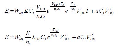
Finally:

We now minimize this energy by writing that the derivative with respect to VDD is zero:
The solution to this equation is not very obvious because, to understand it, we need to know about the existence of the Lambert function as defined by:
This function is shown in Figure 4.9.
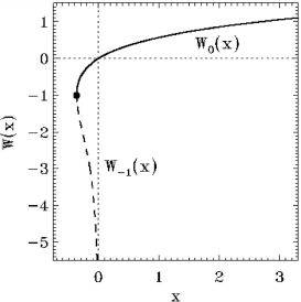
Figure 4.9. Lambert function
Hence, the solution to equation [4.11] is (the calculation is not given in detail):
with:
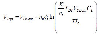
Given that β is greater than the value −1/e, there are two possible solutions for a negative value of β. We will choose the most negative value, which corresponds to the absolute minimum. As the optimal value of VDD has been obtained, it is possible to obtain the corresponding value of VT based on the equation:

So, we find the following:
The condition on the parameter β is not always ensured, particularly for the higher activity rates. In this case, the optimum corresponds to the weakest voltage value, which ensures the logic gate’s functioning. The following section will somewhat clarify things. In practice, the optimal values of approximately 250 mV are obtained in numerous cases.
4.2.2. Limits to sub-threshold CMOS technology
The optimization of the supply voltage can lead to voltage values that are incompatible with the logic gates functioning. The following analysis is aimed at establishing whether two stable states exist within a CMOS sub-threshold inverter or not. It will be done on an inverter chain, writing that the output voltage of one chain inverter is the input voltage of the following inverter. We write the current passing through the inverter when the input voltage is VGS . For the NMOS, we obtain:

For the PMOS, the current is written as:

We note that in this analysis, the output voltage is not necessarily the supply voltage and the input voltage is not necessarily zero. The absolute value of the PMOS voltage is assumed to be egal to that of the NMOS. As the two currents are equal:

This equation allows us to calculate the output voltage according to the input voltage:
The results are given in Figure 4.10.
As the curves represent the output according to the input, the supply voltage is taken as a parameter. The symmetrical curves are traced along the diagonal. They illustrate how an identical inverter functions when out into a series with the first inverter. The output voltage of the first inverter is the input voltage of the second inverter.
The intersection point of the two curves represents that equilibrium state when a large amount of inverters is cascaded. When the supply voltage is high, there are three intersection points. Two of them correspond to the stable states situated on the axes and the third intersection point on the diagonal is associated with a metastable state. When the supply voltage decreases, the stable states are no longer on the axes and they approach the diagonal. The value of  is the ultimate limit. A value of 2n0ϕt is more comfortable. This value can be considered the ultimate limits for the choice of supply voltage in a sub-threshold circuit. In practice, higher values are chosen as they guarantee a minimal operating frequency.
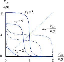
Figure 4.10. Sub-threshold inverter
4.3. Practical and theoretical limits in CMOS technology
4.3.1. Economic considerations and evolving methodologies
Micro-electronic technology progressed at an exponential rate between 1960 and 2000. However, since 2000, there are some significant difficulties, which seem to be in conflict with this progress. They are of very different economic and technical nature. Entire books have been dedicated to analyzing this problem. In this book, the main aim of which is to deal with consumption problems, we will just remind the reader of these different problems and the solutions proposed to combat them.
4.3.1.1. Economic difficulties: the cost of equipment and masks
Investment capacity has always been an issue in the micro-electronics industry. This issue has been made even more difficult to surmount by the exponentially increasing prices due to the reduction in the transistor size. To construct and outfit the foundry of a 14 nm node, the figures can reach up to billions of dollars. The cost of lithography equipment is the main factor responsible for this inflation. The consequence of this is that the amount of players in the micro-electronics sector has significantly decreased. There may be only a few foundries left in the field area of advanced CMOS technologies.
The cost of masks, meaning all of the necessary devices for lithography operations, is also growing at an exponential rate as transistor sizes reduce. As a set of masks are specific to a given type of circuit, this cost cannot be absorbed into the whole production, but instead can only be re-used in the production of identical circuits. Consequently, advanced micro-electronics is only compatible with circuits that can be manufactured and sold in a large series. The amount of new specific circuits (ASIC) is diminishing every year because it is rarely cost-effective to manufacture them in advanced CMOS technology. Programmable circuits have been replacing ASIC in numerous different applications. Integrated generic circuits (processors, DSP, memories), on the other hand, continue to be produced in an increasing rate.
4.3.1.2. Methodological difficulties: the complexity in design and testing
These difficulties are linked to the complexity of associating digital circuits with material and software solutions that need to be combined in a reliable way. Although design tools have progressed a lot, they still have not completely resolved the difficult problem of material–software co-design.
In the 2000s, the test seemed to be a real problem in the development cycle. Progress made at the time in design and test software and in testing equipment reset the boundaries. The flexibility and programmability of current digital circuits also helped to overcome these difficulties. Finally, the significant factor in cycle development became the cost of developing the software.
4.3.1.3. Programming difficulties linked to parallelism
The previous considerations about consumption lead to limiting the operating frequency. The dissipated power P in a circuit of N logic gates is written based on the expression of average dissipated energy E per gate:
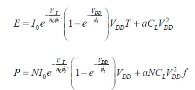
The values I0, a, CL are average values for the set of circuit gates. The frequency effect is, therefore, evident on the dissipated power.
Replacing a circuit made up of a processor and a memory operating at a frequency f with M processors and M memories operating at a frequency f/M is a training exercise, but it explains the procedure quite well. By ignoring the code parallelization difficulties, the system performances are not affected by this operation. The power for the processor–memory group would be P/M and P for the global level. After a rather basic analysis, no gain in power is detected. However, a more accurate analysis will show that the reduced frequency can be accompanied by a decrease in voltage functioning. It will also show that organizing the system into M blocks of reduced size can lead to reduced interconnect lengths and their associated capacitances. Reducing the dissipated power is, therefore, real and has been proven by experience.
The difficulty remains in the software as it is necessary to create in multiprocessor system applications that are generally developed for a monoprocessor system. This technique has made plenty of progress since the 2000s, but it remains to be complex to automate.
4.3.2. Technological difficulties: dissipation, variability and interconnects
4.3.2.1. Heat dissipation
This is the main subject of this book and it is also the main constraint in micro-electronics today. There have been some major consequences from the need to restrict heat production: stagnation in operating frequency; the implementation of parallelism; the introduction of new devices such as the “planar” transistor on the silicon on insulator (SOI) substrate and the FinFET (transistor with a conduction channel that is perpendicular to the substrate) and the progressive introduction of the so-called 3D technologies (using the third dimension to superimpose layers).
Accompanying these transformations is the introduction of new materials: the generalized use of copper in interconnects and the progressive introduction of III–V materials.
Dissipation problems appeared to be very constricting when supply voltage decrease was no longer possible below one volt. In section 4.2, the calculations show that there is an optimal threshold voltage of approximately 300 mV and that it is not useful to go much lower than this voltage. As the supply voltage must be choosen three times the value of the threshold voltage in order to guarantee a suitable operation speed, it is not possible to reduce the supply voltage to below one volt.
4.3.2.2. Controlling the variability
Variability is a statistical phenomenon, the significance of which has been confirmed since the beginning of the 2000s. This phenomenon exacerbates problems related to managing energy consumption so much that the two subjects need to be dealt with simultaneously.
When the transistor size diminishes, statistic dispersions on the transistor parameters increase. The transistor threshold voltage and the delay in a logic gate are well-known examples. These two parameters have a direct impact on the temporal and energy properties of circuits. Variability is a phenomenon that has been known in micro-electronics for a long time, but the consequences for older technologies were only understood in analogic function design and somewhat for specific digital functions. The staple article for understanding this phenomenon is that which was published in 1989 by Marcel Pelgrom [PEL 89]. In this article, Pelgrom shows in a general way that variability varies according to the reverse square root of the conduction transistor’s surface.
Variability expresses that transistors made using the same design rules do not have exactly the same electrical properties, such as the threshold voltage, for example. This difference may be noticed on both sides of the wafer, or in the same place of the wafer but for different wafers. The manufacturing processes are not perfect and it is easy to see that differences in dimensions or physical properties may arise. We need to take these two causes for variation into account when estimating the behavioral differences of these two manufactured circuits in the same “process”, which ideally should be identical.
Let us express the difference in the parameter P for two transistors of the same wafer. This parameter is considered the result of an average on the device’s conduction surface. For example, the average current’s density is the average of the local currents’ densities on the entire surface of the conduction channel:

Each integral can be considered a convolution product with a two-dimension rectangle function. It is also useful to include the Fourier spatial transform of the P (x, y) function. It is written as P(ωx, ωy) and can be broken down into a two-function product, one of the functions being G due to geometry and the other one T due to the process. It can be written that:
For two devices separated by a distance Dx, the dependent geometric term is written as:
The term that is dependent on the process is considered white noise in the spatial sense of the term. The following hypotheses are generally accepted: many elementary events occur, the effects on the parameter are weak and may be summed up and the correlation distance is weak against the device’s dimensions. Variation in doping, mobility, interface charge and thickness of oxide layer are all factors that obey these hypotheses. In this case, the function T(ωx, ωy) can be considered constant in space. Calculating the variance in the difference of the parameter’s value is written as:
For two devices located at a distance  on the wafer, we obtain:
The first term is due to the process variations and the second term is due to the longer distance variations. The coefficients need to be estimated for each parameter considered.
The threshold voltage, the gain factor and the delay are the most frequently considered parameters. The most important conclusion is the dependence that variations have on conduction surface. For very fundamental reasons, miniaturizing components brings about an increase in the dispersion of transistor parameters, as shown in Figure 4.11 (taken from [KIY 09]). This conclusion can also be applied to other components (passive and interconnect) but the effects are not as significant.
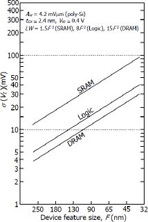
Figure 4.11. Estimating the variability of the threshold voltage as a function of the technological node
We will study two effects of variability: the direct impact on consumption and the impact on time delay in a logic gate, which introduces an indirect effect to dissipation.
The threshold voltage can vary by significant proportions, as it particularly depends on the doping of the semiconductor, as shown in Chapter 3. Let us write the average sub-threshold current in a CMOS circuit as:

For N transistors, the standard deviation for the threshold voltage is σVT, and so the total leakage current is:

Assuming that the probability  is Gaussian, the current is written as:

We can easily obtain:
The leakage current has, therefore, multiplied, which may be significant if the standard deviation of the threshold voltage is greater than  (approximately 40 mV). The static dissipation increases equally. This calculation simply translates the fact that the weakest threshold voltage components contribute significantly to the global consumption, considering the exponential variation in the leakage current with the threshold voltage.
In practice, it is also more important to limit the variability than it is to limit the average dissipation. This is a very important observation, which can help in guiding our choice of technology. Some choices may have a major impact on the average value of the sub-threshold current, such as the example of FinFET with a sub-threshold slope decrease (decrease of the factor n0). Other choices may contribute to a reduced variability (this is the case of the transistor on the SOI substrate, which eliminated the variability due to doping).
Let us now study the effect that variability has on the choice of supply voltage. The delay in logic gates is an important characteristic in circuit design. In fact, when the signals need to be synchronized, it is important to precisely estimate the different delays. If the estimate is imprecise, we will need to either reduce the frequency or diminish the delays and, therefore, also the uncertainties in the delays by increasing the supply voltage. In both cases, the system performances are made worse: the functioning frequency diminishes and the dissipated power increases. A simple model can help in understanding this phenomenon.
The delay in a gate can be modeled in the first order by an expression like:
The results of Chapter 3 explain this entry. The maximum tolerable gap is therefore:

From this, it can easily be deduced that the supply voltage must be greater than VDD min, a value given by the below equation:

The maximum gap for the threshold voltage is due to the variability and can be expressed according to the Pelgrom law, by the equation:

The value of the statistical parameter m can be set to 5.4. A typical value of Δtd max is 1.2:
The variability leads to a growth in supply voltage and then also to a growth in dissipation. In order to reduce the variability, it is possible to act in two ways, which lead to different technological solutions.
The first way consists of getting rid of the main cause of variability: the doping of the base silicon. This also leads to the “planar” transistor becoming completely deserted on the SOI substrate. The second solution consists of maintaining the conduction surface quasi-constant with the miniaturization by a transistor structure in which the conduction channel is no longer in the silicon plan, but instead is perpendicular to this base.
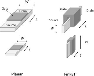
Figure 4.12. Planar transistor on an SOI substrate and a FinFET transistor
This new architecture is called “FinFET”. Placing the width of the transistor in the third dimension allows the surface of the conduction channel to be maintained more easily at a sufficient value, and thus to contain the variability effects. Figure 4.12 illustrates the two options. This is one of the most significant evolutions in micro-electronics since the appearance of enhanced FET. Both technologies have their advantages and disadvantages.
In general, we can say that FinFET technology is very well adapted to fast high-performance circuits (the company INTEL introduced this new structure in 2013), and that SOI technology is well adapted to applications of approximately 500 MHz, in which there are many constraints on dissipation.
4.3.2.3. Evolution of interconnects
Extreme transistor miniaturization leads to a rather paradoxical situation. Transistors’ input capacitances have been diminishing regularly in order to attain values much lower than one fF in regards to logic block transistors and SRAM memories, but after many years of research on dielectric optimization, interconnect capacitances have only attained a quasi-constant value of 2 pF/cm. The only solution for bringing the relative permittivity closer to optimum is to make the insulator as porous as possible. The average length between the two logic gates in a block performing an elementary function diminishes substantially with “scaling” by an obvious geometric effect, which translates into a decreased associated capacitance. The same cannot be said for the connections between the blocks, which mainly depend on the size of the global circuit, a size which does not diminish for complex digital circuits and stays at around cm2. In summary, the decrease in the average capacitance for interconnects does not follow the decrease in the transistor size. The interconnect part in a gate’s average capacitance is rising and consequently the interconnect’s contribution to circuit dissipation is becoming more and more significant.
4.3.3. Theoretical limits and open questions
Transistor miniaturization clearly poses the problem of how to estimate the possible limits. This problem may seem to be purely theoretical, but certain models foresee that the channel length cannot be less than 1.5 nm, which is not different of the effective channel length obtained in current experimental devices. Also remember that the 14 nm node is programmed by the most powerful semiconductor industries. Estimating the possible limits to a field-effect transistor in CMOS technology is, therefore, a real problem. The following section looks again at the results already obtained in Chapter 2, relative to the dissipated power. Other results are based on applying Heisenberg’s uncertainty relation.
4.3.3.1. Limits in applying Shannon’s theorem combined with Heisenberg’s uncertainty relations
Before getting started, note that this section is focused on signal energy and not on dissipated energy. Shannon’s theorem, which was first introduced in 1949 [SHA 49], establishes that, in a transmission channel, it is possible to transmit binary information bits to an amount per second equal to C, by using a somewhat complex coding. The maximum flow of C in this channel is given by the below relation:
where B is the bandwidth, and E and N are the signal energy and the thermal noise in the bandwidth, respectively. Let us recall one of the properties in logarithm function:

From this, it can be deduced that:

As N/B = kBT is defined by thermal noise, we obtain:

A logical operator can be a channel that transmits a given output signal under certain conditions. During a binary transition, a single information bit may be transmitted. This is obvious for an inverter, but also true for another function, such as an AND function. For a transmitted bit, the relation becomes:
The logical signal’s minimal energy is now established. However, this energy is not necessarily dissipated in the form of heat when the adiabatic principle is applied, as shown in Chapter 2.
Now let us consider an ultimate transistor with a single electron passing through the conduction channel. The signal’s energy is, therefore, greater than the minimal value:

The relation of uncertainty applied to an electron assumed to be in the conduction channel can be written as:

If we acknowledge that the uncertainty on velocity is equal to the average velocity value, which is the case for the Poisson law, we obtain:

or
This value gives the minimal channel length; the electron is located in the channel. At room temperature, the minimal length is found to be 1.5 nm. This result allows the smallest transistor to be defined, assuming that the wave function spreading is equal to the channel length. This analysis [ZHI 09] is not unanimously accepted in the scientific community, for the two following reasons in particular: the lack of inclusion of potential energy is not accounted for and the link is not obvious between the spreading of the wave function and the physical dimension of the conduction channel.
These considerations have led a part of the scientific community to question the choice of charge-based devices when the objective is very weak consumption. Instead, what is proposed is the use of spin- or photon-based devices. This approach is also the subject of conflicting discussions.
4.3.3.2. Including the source–drain tunnel effect
When the distance between the source and the drain diminishes, a tunnel effect between the source and the drain may make the gate control seem completely unrealistic [ZHI 09]. This limit may be integrated into the estimate on the minimal transistor size. The transistor is considered a system made up of two potential wells corresponding to the source and the drain, and separated by a potential barrier Eb . The transistor is operational when the passage probability toward the drain is between 0.5 and 1, if the gate imposes a moving state. The model is illustrated in Figure 4.13. The two wells are at a distance of a.
There are two types of probability of transition from the source to the drain: one is of a statistic nature and the other is of a quantum nature. The first probability is written as:

The second probability is written in the WKB approximation, used in quantum mechanics:

The global probability of moving from the source to the drain is therefore:

This probability is equal to 0.5 (approximated calculation not detailed in this section) when the value of the energy barrier is:
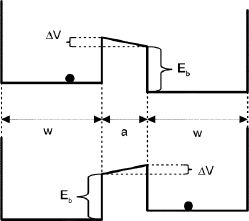
Figure 4.13. Theoretical model of a transistor
This value gives the minimum value for signal’s energy and enables us to obtain the minimum value of the supply voltage. This approximated calculation expresses the supplementary energy cost of eliminating the tunnel effect; even more important is that the channel length is weak. In practice, values greater than 5 nm are necessary to render this surcharge negligible. The hypotheses for the model are open to discussion, but the order of magnitude is there.
4.3.3.3. Necessity for reversible logic
As discussed in Chapter 2, this is the subject of conflicting debates. Energy performances in circuits are currently at five orders of magnitude of the Landauer limit. Therefore, the debate remains to be purely based on theory. However, if new technologies come to replace CMOS technology (such as nano-relay technology, which will be discussed in detail with an example in Chapter 8), reversible logic will be a choice to be considered on the agenda.


