Exploring the different ways to configure a 555 timer chip
Using the 556 dual-timer chip
Building basic 555 timer chip circuits
The 555 timer chip, developed in 1970, is probably the most popular integrated circuit ever made. By some estimates, more than a billion of them are manufactured every year. Its popularity is well deserved. The 555 is a single-chip version of a commonly used circuit called a multivibrator,
which is useful in a wide variety of electronic circuits. You can use the 555 chip for basic timing functions, such as turning a light on for a certain length of time, or you can use it to create a warning light that flashes on and off. You can use it to produce musical notes of a particular frequency, or you can use it to control positioning of a servo device. (You learn about servos in Book 7, Chapter 4
.) The list goes on and on.
In this chapter, you learn how to use this versatile chip in a variety of circuits. First, I explain how the 555 works and what each of its pins do. Then, you see and build a variety of common 555 circuits.
Looking at How the 555 Works
The 555 can be considered a hybrid of an analog and digital circuit. The output produced by a 555 is purely digital: It’s either off (0 V) or it’s on (with positive voltage of at least 2.5 V). The timing mechanism within the 555 determines how long the output is on and how long it’s off.
The analog part of the circuit lies in how you control how long the output signal is on and how long it’s off. You do that by creating an RC network using a resistor and a capacitor. The values you choose for the resistor and capacitor determine the timing interval. I give you all the information you need to choose the correct values for the resistor and capacitor later in this chapter, but if you feel you need a refresher on how RC networks work, please refer to Book 2, Chapter 3
.
You can also control whether the 555 does its timing job just once, like an egg timer, or whether it cycles the output on and off repeatedly, like a metronome that keeps ticking over and over again. You do that by connecting the pins of the 555 chip in various ways.
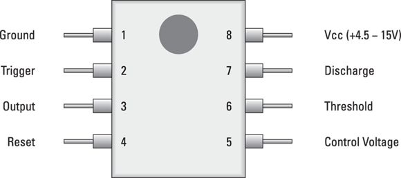
Figure 2-1
shows the arrangement of the eight pins in a standard 555 IC. As you can see, the 555 comes in an 8-pin DIP package.
The following paragraphs describe the function of each of the eight pins (not in numerical order):
Ground:
Pin 1 is connected to ground.
VCC
:
Pin 8 is connected to the positive supply voltage. This voltage must be at least 4.5 V and no greater than 15 V. It’s common to run 555 circuits using four AA or AAA batteries, providing 6 V, or a single 9 V battery.
Output:
Pin 3 is the output pin. The output is either low, which is very close to 0 V, or high, which is close to the supply voltage that’s placed on pin 8. (On some models of the 555, the output voltage may be as much as 2 V below the supply voltage.) The exact shape of the output — that is, how long it’s high and how long it’s low, depends on the connections to the remaining five pins.
For more information about using the output from pin 3, see the section “Using the 555 Timer Output
” later in this chapter.
Trigger:
Pin 2 is the trigger
, which works like a starter’s pistol to start the 555 timer running. The trigger is an active low
trigger, which means that the timer
starts when voltage on pin 2 drops to below one-third of the supply voltage. When the 555 is triggered via pin 2, the output on pin 3 goes high.
For example, if you want to start the timer by pushing a button, you would connect pin 2 to the supply voltage. Then, to trigger the timer, you simply interrupt this supply voltage. There are several ways to do that, but the most common is to connect a normally open push button between pin 2 and ground. Then, the button is pushed, and the supply voltage is short-circuited to ground; so the voltage at pin 2 drops to zero, and the timer is triggered. You see an example of this type of triggering later in this chapter, in the section “Using the 555 in Monostable (One-Shot) Mode
.”
Discharge:
Pin 7 is called the discharge
. This pin is used to discharge an external capacitor that works in conjunction with a resistor to control the timing interval. In most circuits, pin 7 is connected to the supply voltage through a resistor and to ground through a capacitor.
Threshold:
Pin 6 is called the threshold
. The purpose of this pin is to monitor the voltage across the capacitor that’s discharged by pin 7. When this voltage reaches two thirds of the supply voltage (Vcc), the timing cycle ends, and the output on pin 3 goes low.
Control:
Pin 5 is the control
pin. In most 555 circuits, this pin is simply connected to ground, usually through a small
capacitor. (The purpose of the capacitor is to level out any fluctuations in the supply voltage that might affect the operation of the timer.)
In some circuits, a resistor is used between the control pin and Vcc to apply a small voltage to pin 5. This voltage alters the threshold voltage, which in turn changes the timing interval. Most circuits don’t use this capability, however. In this chapter, all the 555 circuits simply connect pin 5 to ground through a
capacitor.
Reset:
Pin 4 is the reset pin, which can be used to restart the 555’s timing operation. Like the trigger input, reset is an active low input. Thus, pin 4 must be connected to the supply voltage for the 555 timer to operate. If pin 4 is momentarily grounded, the 555 timer’s operation is interrupted and won’t start again until it’s triggered again via pin 2.
When used in a schematic diagram, the pins of a 555 timer chip are almost always shown in the arrangement depicted in Figure 2-2
. As you can see, this arrangement follows the customary order of elements in a schematic diagram: Supply voltage is at the top, ground is at the bottom, inputs are at the left, and outputs are at the right. This arrangement makes it easy to determine the operation of the circuit from the schematic diagram.
FIGURE 2-2:
How a 555 timer chip is usually shown in a schematic diagram.
Understanding 555 Modes
There are three basic ways — called modes
— that you can wire up a 555 timer IC:
Monostable mode:
Works like an egg timer. When you start it, the timer turns on the output, waits for the time interval to elapse, and then turns the output off and stops.
Astable mode:
Works like a metronome: It keeps running until you turn it off.
Bistable mode:
Isn’t really a timer mode. Instead, it uses the trigger input to alternately turn the output on and off. This type of circuit is often called a flip-flop
and is very commonly used in digital electronics.
The following sections explain how each of these three operating modes work.
Using the 555 in Monostable (One-Shot) Mode
Monostable mode
lets you use the 555 timer chip as a single-event timer. This mode is called monostable
because when wired this way, the 555 has just one stable mode, with the output at pin 3 off. When the 555 is sent a trigger pulse, this
stable state is temporarily interrupted for an interval that’s determined by the value of a resistor and a capacitor. During this interval, the output at pin 3 goes high, but once the time interval has passed, the 555 returns to its stable state, with pin 3 going low.
Monostable mode is sometimes called one-shot mode,
which seems a little more descriptive to me. One-shot mode
conveys the idea that when triggered, the 555 gives one and only one output pulse. When the time interval is reached, the output pulse stops, and the circuit goes quiet until another trigger pulse is detected. Each trigger pulse results in a single output pulse.
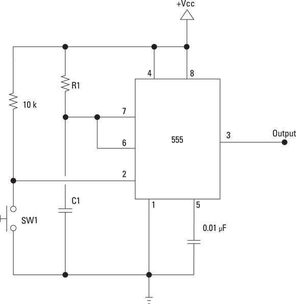
Looking at a typical 555 monostable circuit
Figure 2-3
shows the typical wiring for a 555 timer used in monostable mode.
To understand how this circuit works, first look at the way the
resistor and the switch are wired to pin 2, the trigger input. The switch is a normally open push button. When the button isn’t depressed, the
resistor provides a voltage input to pin 2, which keeps the trigger input high. With the trigger input high, the output voltage at pin 3 is near zero.
When the push-button switch is depressed, the supply voltage is short-circuited to ground. This causes the voltage at pin 2 to drop to zero, and the timer is triggered. Once the timer is triggered, the output voltage at pin 3 goes high and the timing interval begins.
Looking at the resistor-capacitor circuit in a monostable timer
Now that you understand how the trigger circuit works, look at how the RC circuit (R1 and C1) works. The resistor and capacitor work together to determine how long the output will remain high. In a nutshell, once the circuit is triggered, C1 begins to charge.
Pins 6 and 7 — the threshold and discharge pins — are tied together in a monostable 555 circuit. Pin 6 watches the voltage across the capacitor. As the capacitor charges, this voltage increases. When the capacitor voltage reaches two thirds of the Vcc supply voltage, the timing cycle ends, and the output at pin 3 goes low.
The discharge pin (pin 7), charges and discharges the capacitor. To understand how pin 7 works, it may be helpful to visualize the internal workings of pin 7 using the model shown in Figure 2-4
. Here, pin 7 is connected to a switch that’s controlled by the status of the output at pin 3. When the output is high, the switch is open; when the output is low, the switch is closed. When the switch is closed, a small
resistor within the 555 connects pin 7 to ground. (This isn’t really a switch inside the 555, but this model may help you understand how pin 7 works.)
FIGURE 2-4:
The imaginary switch inside the 555 that controls whether pin 7 charges or discharges the capacitor.
When the output on pin 3 is low, the imaginary switch inside the 555 is closed, and pin 7 is connected to ground through the
resistor. This allows the voltage on C1 to discharge through the 555.
But when the output on pin 3 goes high, the imaginary switch inside the 555 is opened. This forces the current flowing through R1 to go through C1, which in turn causes the capacitor to charge at a rate that depends on the values of R1 and the capacitor.
While the capacitor is charging, pin 6 monitors the voltage that builds up across the capacitor. Once this voltage reaches two-thirds of the supply voltage, pin 6 signals the 555 that the timing interval is ended, and the output goes low. This, in turn, closes the imaginary switch inside the 555, which allows the capacitor to discharge.
Calculating the time interval for a monostable circuit
The time interval for a 555 monostable circuit is a measure of how long the output stays high when it’s triggered. To calculate the time interval, just use this formula:
Here, T is the time interval in seconds, R is the resistance of R1 in ohms, and C is the capacitance of C1 in farads.
For example, suppose R1 is
, and C1 is
. Then, you would calculate the time interval like this:
Thus, the circuit will stay on for 5.5 seconds after it’s triggered.
When you make this calculation, it’s imperative that you use the correct number of zeros for both the resistance and the capacitance. Use Table 2-1
as a guide:
TABLE 2-1
Conversion of Resistance and Capacitance Values
Resistance
Capacitance
If you don’t want to do these calculations yourself, you can find 555 timer calculators on the web. Just go to Google or any other search engine and search 555 timer calculator.
Using the 555 in Astable (Oscillator) Mode
Another common way to use a 555 timer is in astable mode.
The term astable
simply means that the 555 has no stable state: Just as it gets settled into one state (say, the output at pin 3 high), it switches to the opposite state (output low). Then it switches back to the first state, and so on, ad infinitum. This mode is also called oscillator mode,
because it uses the 555 as an oscillator, which creates a square wave signal.
Looking at a typical astable circuit
Figure 2-5
shows the basic circuit for a 555 in astable mode.
To understand how this circuit works, first notice that the trigger pin (pin 2) is connected directly to C1. In the monostable circuit, the timer was triggered by a switch that short-circuited the voltage applied to pin 2. In the astable circuit, the timer is triggered when the capacitor discharges — once the voltage across the capacitor drops to one-third of the supply voltage, pin 2 triggers the timer to start another cycle.
Here I examine how this timing cycle works, step by step, starting with the output at pin 3 in the high condition.
With the output high, the discharge pin (pin 7) is open, forcing current through resistors R2 and C1. This causes the capacitor to charge at a rate that depends on the combined value of R1 and R2 and the value of C1.
As the capacitor charges, the voltage at pins 2 and 6 increases.
When the voltage at pin 6 (the threshold pin) reaches two-thirds of the supply voltage, the threshold circuitry within the 555 causes the output voltage at pin 3 to go low.
When the output at pin 3 goes low, the discharge pin (pin 7) is connected to ground within the 555. This allows C1 to discharge. This discharge occurs through R2, so the value of R2 as well as the value of the capacitor determines the rate at which the capacitor discharges.
As the capacitor discharges, the voltage at pins 2 and 6 decreases.
When the voltage at pin 2 (the trigger pin) drops to one third of the supply voltage, the trigger circuitry inside the 555 causes the output at pin 3 to go high.
When the output at pin 3 goes high, the discharge pin (pin 7) is opened, and the cycle starts over again.
Controlling the time intervals in an astable 555 circuit
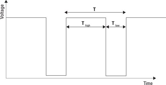
The output of a 555 circuit in astable mode is a square wave, as depicted in Figure 2-6
. There are three important time measurements for a square wave:
T:
The total duration of the wave, measure from the start of one high pulse to the start of the next high pulse.
Thigh
:
The length of the high portion of the cycle.
Tlow
:
The length of the low portion of the cycle.
FIGURE 2-6:
Timing the output wave created by an astable 555 timer circuit.
Naturally, the total time T is the sum of Thigh
and Tlow
.
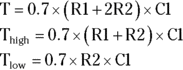
The values of these time constants depend on the values for the two resistors (R1 and R2) and the C1.
Here are the formulas for calculating each of these time constants:
There’s an interesting fact buried in these calculations that you need to be aware of: C1 charges through both R1 and R2, but it discharges only through R2. That’s why you must add the two resistor values for the Thigh
calculation, but you use only R2 for the Tlow
calculation. It’s also why you must double R2 but not R1 for the total time (T) calculation.
Now, plug in some real numbers to see how the equations work out. Suppose both resistors are
and the capacitor is
. Then, the total length of the cycle is calculated like this:
Thus, the total cycle time will be 2.1 s, with the output high for 1.4 s and low for 0.7 s.
If you want, you can also calculate the frequency of the output signal by dividing the total cycle time into 1. So, for the above calculations, the frequency is 0.47619 Hz.
If you use smaller resistor and capacitor values, you’ll get shorter pulses and higher output frequencies. For example, if you use
resistors and a
capacitor, the output signal will be 48 kHz, and each cycle will last just a few millionths of a second.
You may have also noticed that if the two resistors are the same value, the signal will be high for twice as long as it’s off. By using different resistor values, you can vary the difference between the high and low portions of the signal.
Calculating the duty cycle
The duty cycle
in a 555 circuit is the percentage of time that the output is high for each cycle of the square wave. For example, if the total cycle time is 1 s and the output is high for the first 0.4 s of each cycle, the duty cycle is 40%.
With an astable circuit such as the one shown in Figure 2-5
, the duty cycle must always be greater than 50%. In other words, the duration for which the output is high must always be more than the duration during which the output is low.
The explanation for this is pretty simple: For the duty cycle to be 50%, the capacitor would have to charge and discharge through the same resistance. The only way to accomplish that would be to omit R1 altogether, so that the capacitor charged and discharged through R2 only. But the problem with that is that you would end up connecting pin 7 directly to Vcc. With no resistance between pin 7 and the voltage source, the current flowing through pin 7 would exceed the maximum that can be handled by the circuitry inside the 555, and the chip would be damaged.
There’s a clever way around this limitation: Place a diode across R2, as shown in Figure 2-7
. This diode bypasses R2 when the capacitor is charged. That way, the capacitor charges through R1 and discharges through R2.
FIGURE 2-7:
Using a diode to separately control the high and low part of the output signal.
When a diode is used in this way, you have complete control over the duration of both the charge and discharge time. If R1 and R2 have the same value, the capacitor takes the same amount of time to charge as it does to discharge, so the duty cycle will be 50%. If R2 is smaller than R1, the duty cycle is less than 50% because the capacitor discharges faster than it charges.
If you use the diode as depicted in Figure 2-7
, you must adjust the formulas for calculating the time intervals as follows:
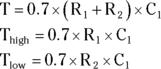
Using the 555 in Bistable (Flip-Flop) Mode
A flip-flop
is a circuit that alternates between two output states. In a flip-flop, a short pulse on the trigger causes the output to go high and stay high, even after the trigger pulse ends. The output stays high until a reset pulse is received, at which time the output goes low.
This type of circuit is called bistable
because the circuit has two stable states: high and low. The circuit stays low until it’s triggered. Then, it stays high until it’s reset. This type of circuit is used extensively in computers and other digital circuits.
For computer applications, the 555 is a poor choice for use as a flip-flop. That’s because its output doesn’t change fast enough in response to trigger or reset pulses in computer circuits that are driven by high-speed clock pulses. For computer applications, better flip-flop chips are readily available, as you learn in Book 5, Chapter 4
.
That being said, the 555 is often used in bistable mode for noncomputer applications where high-speed response isn’t necessary. For example, imagine a simple robot that drives itself forward until it bumps into something in front of it, and then drives backward until it bumps into something behind it. The robot would be equipped with contact switches on the front and rear connected to the trigger and reset inputs of a 555 in bistable mode. The robot’s drive motor would be connected to the output such that when the output is low, the motor runs forward, and when the output is high, the motor runs backward. Then, the bistable 555 would cause the robot to drive back and forth between two obstacles.
Figure 2-8
shows the schematic for a 555 used in bistable mode. As you can see, this circuit doesn’t require a capacitor. That’s because in bistable mode, the 555 isn’t used as a timer. The highs and lows of the output signal are controlled by the trigger and reset inputs, not by the charging and discharging of a capacitor.
FIGURE 2-8:
The schematic for a 555 timer circuit in bistable mode.
Both the trigger (pin 2) and the reset (pin 4) inputs are connected to Vcc through a
resistor. When the set switch is depressed, pin 2 is shorted to ground. This
causes the voltage to bypass pin 2, resulting in a momentary low pulse, which triggers the 555. Once triggered, the output pin goes high.
In astable or monostable mode, the output pin would remain high until the voltage at the threshold pin (pin 6) reaches two-thirds of the supply voltage. However, because pin 6 isn’t connected to anything in this circuit, no voltage is ever present on pin 6. Thus, the threshold is never reached, so the output remains high indefinitely until the 555 is reset by a low pulse on the reset pin (pin 4).
The reset input (pin 4) is connected to Vcc in the same manner as the trigger input. As a result, when the reset switch is pressed, pin 4 is short circuited to ground, creating a low pulse, which resets the 555 and brings the output back to low.
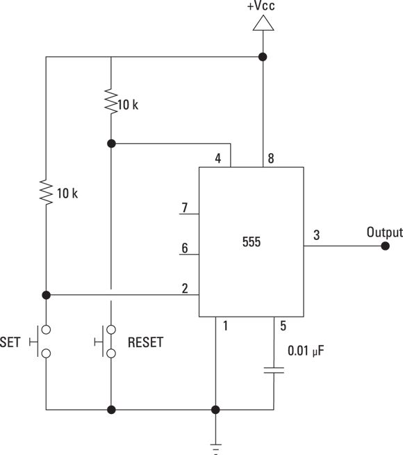
Using the 555 Timer Output
The output pin (pin 3) of a 555 can be in one of two states: high or low. In the high state, the voltage at the pin is close to the supply voltage. The low state is 0 V.
There are two ways you can connect output components to the output pin. Figure 2-9
illustrates these two configurations, using an LED as the output device. A resistor is also included in the circuit to limit the current flow. Without the resistor, current will flow through the circuit unimpeded, which will quickly burn out the LED and probably ruin the 555 as well.
FIGURE 2-9:
Sourcing and sinking output current for a 555 timer.
In the circuit on the left, current flows through the LED circuit when the output is high. The current flows from the output pin through the LED and resistor to ground. This output configuration is called sourcing
because the 555 is the source of the current that drives the output.
In the circuit on the right, current flows through the LED circuit when the output is low. The current flows from the Vcc supply, through the LED and resistor, and into the 555 where it’s internally routed to ground through pin 1. This output configuration is called sinking
because the current is sent into the 555.
Whether you source or sink your output circuit depends on whether you want your output circuit to turn on when the output is high or low.
Figure 2-10
shows that you can combine both sourcing and sinking in a single circuit. Here, two LEDs are connected to the output pin. One is sourced; the other is sunk. In this circuit, the LEDs alternately flash as the output switches from high to low. LED1 lights when the output is low, LED 2 when the output is high.
FIGURE 2-10:
You can combine sourcing and sinking current for the output of a 555 timer.
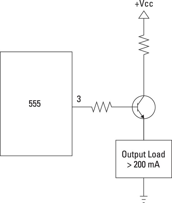
The output circuit of a 555 timer can handle as much as 200 mA of current, which is actually much more current than most integrated circuits can source or sink. If you need to drive a device that requires more than 200 mA, you can isolate the output device from the 555 by using a transistor, as shown in Figure 2-11
. For more information about working with transistors, please refer to Book 2, Chapter 6
.
FIGURE 2-11:
Using a transistor to drive a higher-current device.
Doubling Up with the 556 Dual Timer
If one 555 timer chip is good, two are even better! In fact, it turns out that there are many uses for two (or more) 555 timers in a single circuit — useful enough that you can get two 555 timers in a single chip, called the 556 dual-timer chip.
The 556 dual-timer chip comes in a 14-pin DIP package. The two 555 timers share a common supply and ground pin. The remaining 12 pins are allocated to the inputs and outputs of the individual 555 timers. Table 2-2
lists the pin connections for each of the 555 timers in a 556 dual-timer chip. As an added bonus (no charge!), I also list the pinouts for a standard 555 timer chip in Table 2-2
.
TABLE 2-2
Pinouts for the 555 Timer and 556 Dual-Timer Chips
Function
555 Timer
556 First Timer
556 Second Timer
Ground
1
7
7
Trigger
2
6
8
Output
3
5
9
Reset
4
4
10
Control
5
3
11
Threshold
6
2
12
Discharge
7
1
13
Vcc
8
14
14
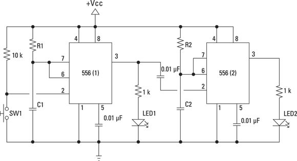
One common way to use a 556 dual timer is to connect both 555 circuits in monostable (one-shot) mode, with the output pin from the first 555 timer connected to the trigger pin of the second 555 timer. Then, when the output of the first timer goes low, the second timer is triggered. You can connect as many 555 timers as you want in this way, with each timer’s output connected to the next timer’s trigger so that the timers work in sequence, one after the other.
For example, Figure 2-12
shows a cascaded timer circuit that uses two separate 555 timer chips. In this circuit, both of the 555 timer chips are configured in monostable mode, much like the circuit in Figure 2-3
. The time interval for the first 555 is controlled by R1 and C1. For the second 555, the interval is controlled by R2 and C2. You can choose whatever values you want for these components to achieve whatever time intervals suit your fancy.
The first 555 chip is triggered when SW1 is depressed, taking pin 2 to ground. This takes the output on pin 3 high, which lights LED1. Notice, however, that pin 3 of the first 555 is connected through a small capacitor to the trigger input of the second 555. As soon as the time interval expires on the first 555, its output goes low, which turns off LED1 and at the same time triggers the second 555, which in turn lights up LED2. LED2 stays lit until C2 charges, and then it goes out. The circuit then waits to be triggered again by a press of the switch.
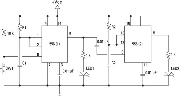
Figure 2-13
shows how this same circuit can be implemented using a single 556 dual-timer chip. This schematic is nearly identical to the schematic shown in Figure 2-13
, but with a few important differences:
The two 555 timer circuits are designated as 556 (1)
and 556 (2)
to indicate that these timer circuits are part of a single 556 dual-timer chip.
The pin numbers indicate the pin assignments for the two timer circuits of a 556 instead of the pin assignments for a 555.
The second timer circuit doesn’t show a supply or ground connection. That’s because the two timer circuits share a common supply and ground connection, which is shown connected to the first timer.
FIGURE 2-13:
The two halves of a 556 dual-timer circuit can be cascaded.
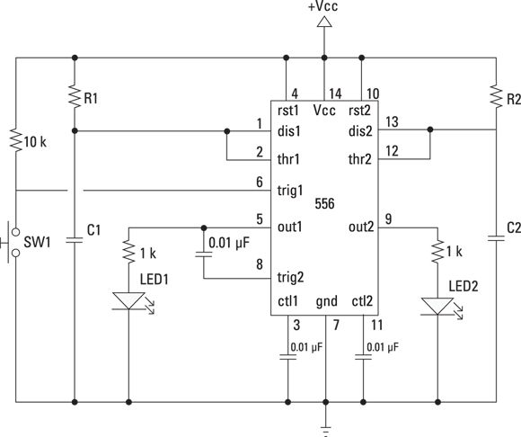
Although it’s convenient to show the two halves of a 556 dual timer as separate components in a schematic diagram, you can show the 556 as a single component if you want. Figure 2-14
shows how the schematic for the cascaded timer circuit can be drawn using a single component for the 556 dual timer. This circuit is nearly identical to the circuit shown in Figure 2-13
; the only difference is the way the schematic depicts the two sections of the 556 dual-timer chip.
FIGURE 2-14:
The cascaded timer circuit with the 556 dual-timer chip drawn as a single component.
When you draw a 556 as a single component, it’s helpful to draw the connections for the two timers on opposite sides of the component. In Figure 2-14
, I drew the connections for the first timer on the left and the second timer on the right, with the exception of the trigger input for the second timer (pin 8). Drawing that connection on the right side of the component would complicate the diagram, so I placed it on the left side just beneath the output pin for the first timer.
Because it’s difficult to keep track of which pin is which in a 556, it’s helpful to label the function of each pin as I did in the schematic shown in Figure 2-14
.
Making a One-Shot Timer
In this section, you build a circuit that uses a 555 timer chip in monostable mode. When a trigger switch is pressed, an LED lights and stays lit for approximately 5 seconds. Then, the LED goes dark until the button is pressed again.
Project 21 provides all the information you need to assemble this circuit. The circuit is based on the schematic for the monostable circuit that was shown in Figure 2-3
. The only differences are that an LED is added to the output pin (pin 3) and the resistor, and capacitor values are included in the capacitor charging circuit.
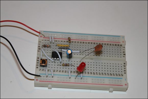
When you are finished, the circuit will look like Figure 2-15
. To test the circuit, push the push button. The LED should light, stay lit for just over 5 seconds, and then go back off. It should light again only when you press the push button again.
FIGURE 2-15:
The finished one-shot timer project (Project 21).
If the circuit doesn’t work, here are a few things to check:
Make sure the battery is good. (Use a voltmeter to test it.)
Carefully double-check all the jumper wires and other components to make sure they’re connected properly.
Make sure the LED isn’t inserted backwards. As a test, pull it out and insert it with the leads reversed.
Make sure the electrolytic capacitor is inserted with the negative end on ground side of the circuit.
Make sure the solder connections to the push button are solid.
Project 21: A One-Shot 555 Timer Circuit
In this project, you build a circuit that uses a 555 timer chip in monostable mode to create a one-shot timer. The circuit includes a push button and an LED. When you press the push button, the LED will turn on and stay on for about 5 seconds. Then the LED will turn off and stay off until you press the push button again.
The only tools you’ll need to complete this project are wire cutters and wire strippers.
Parts
One 9 V battery
One 9 V battery snap holder (RadioShack 2700325)
One small solderless breadboard (RadioShack 2760003)
One normally open push-button switch
One 555 timer chip (RadioShack 27617185)
One 5mm red LED (RadioShack 2760209)
One
resistor (brown-black-orange)
One
resistor (yellow-violet-brown)
One
resistor (yellow-violet-yellow)
One
electrolytic capacitor
One
ceramic disk capacitor
One normally open DIP breadboard push button
Eight jumper wires (various lengths)
Steps
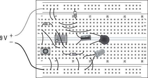
Throughout these steps, use the negative (–) bus strip at the bottom of the board for ground and the positive (+) bus strip on the top of the board as the positive voltage.
Insert the 555 timer chip.
Insert the chip so that it straddles the gap in the center of the solderless breadboard, with pin 1 in hole E5 and pin 8 in hole F5.
Insert the jumper wires.
If you’re using precut jumper wires, choose an appropriate length for each segment. Otherwise, cut your own jumper wires as needed. You need a total of eight jumper wires, inserted into the solderless breadboard as follows:
From
To
A3
Ground bus
A5
Ground bus
A11
Ground bus
A15
Ground bus
J4
+ voltage bus
J5
+ voltage bus
E1
F1
D6
G1
D8
G5 (Note that this wire crosses over the top of the 555.)
G8
G15
H7
H11
I6
I11
Insert the resistors.
Insert the three resistors as follows:
Resistor
From
To
H1
H4
J11
+ voltage bus
C7
C13
Insert the capacitors.
Insert the two capacitors as follows:
Capacitor
From
To
E11
F11
E15
F15
Make sure the negative lead of the electrolytic capacitor is in hole E11.
Insert the LED.
The anode (the long lead) should be inserted in hole A13, and the cathode (the short lead) in the ground bus.
Insert the push button.
Insert the push button in holes B1, D1, B3 and D3. (Ensure that the switch is oriented such that it closes from B1/D1 to B3/D3.)
Connect the battery.
Plug the 9 V battery into the battery snap connector, and then connect the red lead to the positive voltage bus and the black lead to the ground bus.
You’re finished! You can now press the button to turn on the LED. The LED will go dark again after about 5 seconds.
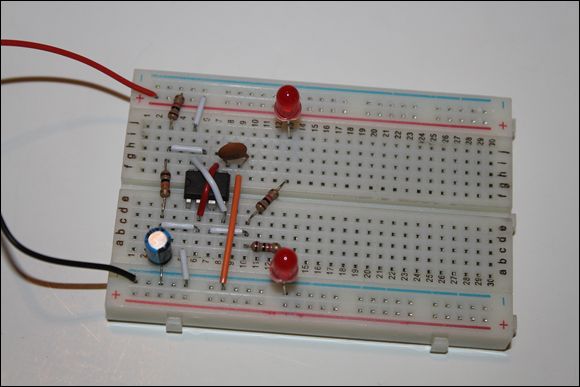
Making an LED Flasher
In this section, you build a circuit that uses a 555 timer chip to alternately flash two LEDs on and off. For this circuit, the 555 is configured in 555 in astable mode, and the resistor values are chosen so that they cause the high and low timings to be very close to one another, about one-tenth of a second each.
Project 22 shows you how to build the LED flasher circuit. The schematic for this project is similar to the one that was shown in Figure 2-5
, but adds a pair of LEDs to the output circuit. LED1 lights when the output is high, and LED2 lights when the output is low. Note that this circuit uses both sinking and sourcing of the output current.
FIGURE 2-16:
The finished LED flasher (Project 22).
If the circuit doesn’t work, here are a few things to check:
Check the battery voltage.
Double-check all the jumper wires and resistors to make sure they’re inserted in the proper holes.
Make sure the diodes and the electrolytic capacitor are inserted correctly. For the LEDs, the anodes must be on the positive side of the circuit and the cathodes on the negative side. For the capacitor, the negative side must be in the ground bus.
After you finish playing with the completed project, you may want to leave it assembled. The next section (Project 23) adds a second 555 timer to this circuit to include additional functionality.
Project 22: An LED Flasher
In this project, you build a circuit that alternately flashes a pair of LEDs. The circuit uses a 555 timer configured in astable mode to flash the LEDs. The resistor and capacitor values are chosen so that the duty cycle is close to 50 percent and each LED stays on for about one-tenth of a second.
The only tools you’ll need to complete this project are wire cutters and wire strippers.
Parts
One 9 V battery
One 9 V battery snap holder (RadioShack 2700325)
One small solderless breadboard (RadioShack 2760003)
One 555 timer chip (RadioShack 27617185)
Two 5mm red LEDs (RadioShack 2760209)
One
resistor (brown-black-orange)
Three
resistors (brown-black-red)
One
electrolytic capacitor
One
ceramic disk capacitor
Eight jumper wires (various lengths)
Steps
Insert the 555 timer chip.
Insert the chip so that it straddles the gap in the center of the solderless breadboard, with pin 1 in hole E5 and pin 8 in hole F5.
Insert the jumper wires.
If you’re using precut jumper wires, choose an appropriate length for each segment. Otherwise, cut your own jumper wires as needed. You need a total of eight jumper wires, inserted in the solderless breadboard as follows:
From
To
A5
Ground bus
C3
C6
C7
C10
D6
G7 (This wire crosses over the top of the 555.)
D8
G5 (This wire also crosses over the top of the 555.)
H3
H6
F9
Ground bus
J5
+ voltage bus
Insert the resistors.
Insert the four resistors as follows:
Resistor
From
To
D3
G3
J3
+ voltage bus
B10
B13
D10
F13
Insert the capacitors.
Insert the two capacitors as follows:
Capacitor
From
To
G8
G9
A3
Ground bus
Make sure the negative lead of the electrolytic capacitor is in the ground bus.
Insert the LEDs.
Insert the two LEDs as follows:
LED
Cathode (Short Lead)
Anode (Long Lead)
LED1
J13
+ voltage bus
LED2
Ground bus
A13
Connect the battery.
Plug the 9 V battery into the battery snap connector, and then connect the red lead to the positive voltage bus and the black lead to the ground bus. The LEDs should begin flashing immediately when the battery is connected.
You’re finished!
After you finish this project, leave it assembled if you intend to build Project 23.
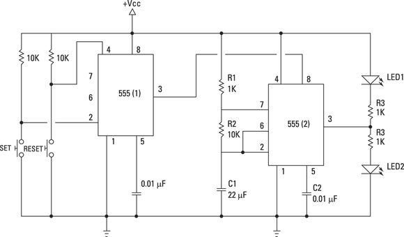
Using a Set/Reset Switch
In this section, you modify the circuit that you built in Project 22 so that the circuit is controlled by two push buttons that function as a set/reset switch. When you connect the power to this circuit, LED1 turns on and stays on. When you press the set push button, the two LEDs start flashing alternately and continue to flash until you press the reset push button.
The circuit for this project uses two 555 timer chips. The first is configured in bistable mode with two push buttons acting as set and reset switches. The second is configured in astable mode, almost identical to the 555 timer that was used in Project 22. The difference is that instead of connecting the astable 555 Timer chip’s supply voltage pin (pin 8) directly to the battery, it is connected to the output of the first 555. Thus, the first 555 controls the power to the second 555, so the second 555 flashes the LEDs only when the output of the first 555 is high.
This project requires that you use two push-button switches that are not designed to be inserted into a solderless breadboard. To make the switches easier to use with the breadboard, solder short lengths of 20-gauge solid wire to the switch terminals.
Project 23 shows you how to build this circuit, and the completed project is pictured in Figure 2-17
.
FIGURE 2-17:
The completed circuit for Project 23.
Project 23: An LED Flasher with a Set/Reset Switch
In this project, you expand the circuit you built in Project 22 to add a set/reset switch that controls the flashing of the LEDs. You should build Project 22 before you attempt this project.
The only tools you’ll need to complete this project are wire cutters and wire strippers.
Parts
You will need all the parts from Project 22, plus the following:
One 555 timer chip (RadioShack 27617185)
Two
resistors (brown-black-orange)
One
ceramic disk capacitor
One normally open momentary contact push button (RadioShack 2751547)
Eight jumper wires (various lengths)
Steps
If you haven’t already done so, build the LED flasher circuit described in the preceding section.
The 555 timer chip in that project is the one designated as 555 (2)
for this project.
Remove the jumper wire you inserted from hole J5 to the positive bus.
This step disconnects the Vcc supply (pin 8) of 555 (2). Voltage for 555 (2) is provided by the output of 555 (1).
Insert the second 555 chip.
Insert the chip so that it straddles the gap in the center of the solderless breadboard, with pin 1 in hole E17 and pin 8 in hole F17.
Insert the additional jumper wires.
If you’re using precut jumper wires, choose an appropriate length for each segment. Otherwise, cut your own jumper wires as needed. You need a total of eight additional jumper wires, inserted into the solderless breadboard as follows:
From
To
A17
Ground bus
I5
D19
C18
I27
B20
H30
F21
Any hole in the ground bus
A25
Ground bus
A28
Ground bus
Insert the resistors.
Insert the two resistors as follows:
Resistor
From
To
J27
+ voltage bus
J30
+ voltage bus
Insert the capacitor.
The
capacitor should be inserted in holes G20 and G21.
Insert the push buttons.
Insert the two push-button switches so that they straddle the gap, as follows:
Button
Location
Set
E25, F25, E27, F27
Reset
E28, F28, E30, F30
Connect the battery.
Plug the 9 V battery into the battery snap connector, and then connect the red lead to the positive voltage bus and the black lead to the ground bus. LED1 should immediately light up. (If it doesn’t, double-check all your connections and make sure the battery isn’t dead.)
You’re done!
Press the set button to start the LEDs flashing. Let them flash for a while, and then press the reset button to make the flashing stop.
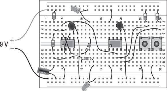
Making a Beeper
In this section, you use two 555 timer chips to build an audible beeper, with both timers configured in astable mode. One timer generates an audible square-wave tone that is sent to a speaker so the tone can be heard. The other timer generates a much slower frequency that is connected to the reset of the first timer to turn the tone on and off, which creates the beeping effect.
Project 24 shows how to build this circuit. Before you start, have a look for a moment at the project’s schematic diagram. For the first timer chip — designated 555 (1)
in the schematic — the RC network uses resistors of
and
along with a
capacitor to produce the 1.5Hz output. The second timer — 555 (2)
— uses
and a
resistors and a
capacitor to create the output tone. The output of the first timer is sent to the reset of the second timer, and the output of the second timer is sent through a
capacitor to an
speaker.
Note:
You could easily build this circuit using a single 556 dual-timer chip. You’d have to adjust the pin designations on the schematic accordingly.
The speaker used in this circuit can be any
speaker. If you have an old unamplified computer speaker, you can use it. I recommend you solder 2- to 3-inch lengths of 20-gauge solid wire to the speaker terminals so you can easily connect the speaker to the breadboard.
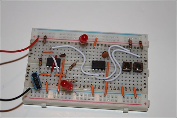
FIGURE 2-18:
The completed beeper project (Project 24).
Here are some extra-credit assignments for this project, in case you want to experiment with the circuit a bit:
Try building the circuit with a single 556 chip instead of two 555 chips.
Replace the
R3 with a
resistor, and then add a
potentiometer in series with the resistor. As you turn the potentiometer, the tone changes.
Add a
potentiometer in series with R1. Then, as you turn the potentiometer, the beeping rate changes.
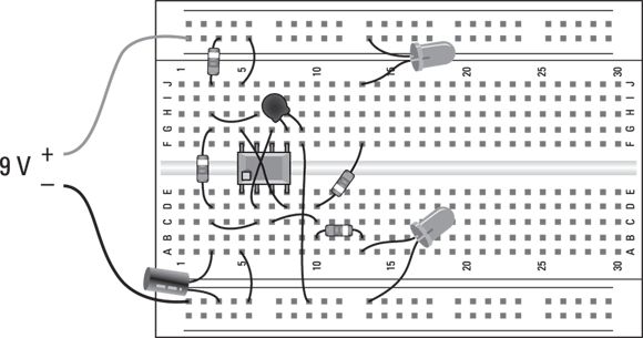
Project 24: An Audible Beeper
In this project, you use a pair of 555 timer ICs to build a circuit that produces an audible beep on a small speaker. Both of the 555 timer ICs are configured in astable mode. The first 555 provides the beeping interval, which is about one beep every one-tenth of a second. The second 555 generates an audible frequency that’s fed to the speaker to produce the output tone.
To build this project, you’ll need wire cutters and wire strippers.
Parts
One 9 V battery
One 9 V battery snap holder (RadioShack 2700325)
One small solderless breadboard (RadioShack 2760003)
Two 555 timer chips (RadioShack 2761718)
One
resistor (brown-black-red)
One
resistor (yellow-violet-yellow)
One
resistor (yellow-violet-red)
One
resistor (brown-green-orange)
One
electrolytic capacitor
One
electrolytic capacitor
Two
ceramic disk capacitors
One 8-ohm speaker
15 jumper wires (various lengths)
Steps
Insert the 555 timer chips.
Insert the chips so that they straddle the gap in the center of the solderless breadboard. For the first chip, insert pin 1 in hole E5 and pin 8 in hole F5. For the second chip, insert pin 1 in hole E17 and pin 8 in hole F17.
Insert the jumper wires.
If you’re using precut jumper wires, choose an appropriate length for each segment. Otherwise, cut your own jumper wires as needed. You need a total of 15 jumper wires, inserted into the solderless breadboard as follows:
From
To
A5
Ground bus
A17
Ground bus
J5
Positive (+) voltage bus
J17
+ voltage bus
C3
C6
H3
H6
C15
C18
G15
G18
F9
Ground bus
E10
Positive (+) voltage bus
D8
D10
D6
G7 (This wire crosses over the top of the first 555 chip.)
D18
G19 (This wire crosses over the top of the second 555 chip.)
F21
Ground bus
Insert the resistors.
Insert the four resistors as follows:
Resistor
From
To
J3
Positive (+) voltage bus
E3
F3
J15
Positive (+) voltage bus
E15
F15
Insert the capacitors.
Insert the five capacitors as follows:
Designation
Capacitor
From
To
C1
Electrolytic
A3
Ground bus
C2
Ceramic Disk
G8
G9
C3
Ceramic Disk
A15
Ground bus
C4
Ceramic Disk
G20
G21
C5
Electrolytic
D19
D23
Note that for C1, the negative lead should be inserted into the ground bus. For C5, the negative lead should be in D23.
Connect the speaker.
One lead from the speaker should be inserted in hole B23. The other can be inserted in any hole in the ground bus.
Note that speakers aren’t sensitive to polarity, so it doesn’t matter which lead goes in the ground bus and which goes in B23.
Connect the battery.
Plug the 9 V battery into the battery snap connector, and then connect the red lead to the positive voltage bus and the black lead to the ground bus. You should immediately hear the speaker beeping.
You’re finished!
Remove the battery when you can no longer stand the beeping.
 Learning about the 555 timer chip
 capacitor. (The purpose of the capacitor is to level out any fluctuations in the supply voltage that might affect the operation of the timer.)
 capacitor.
 When used in a schematic diagram, the pins of a 555 timer chip are almost always shown in the arrangement depicted in
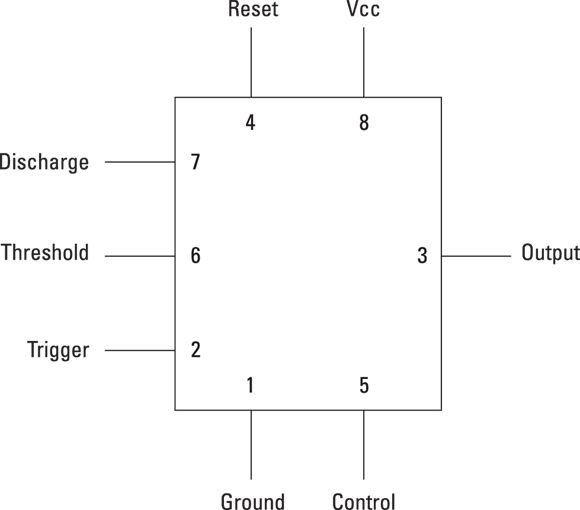
 resistor and the switch are wired to pin 2, the trigger input. The switch is a normally open push button. When the button isn’t depressed, the
  resistor provides a voltage input to pin 2, which keeps the trigger input high. With the trigger input high, the output voltage at pin 3 is near zero.
 resistor within the 555 connects pin 7 to ground. (This isn’t really a switch inside the 555, but this model may help you understand how pin 7 works.)
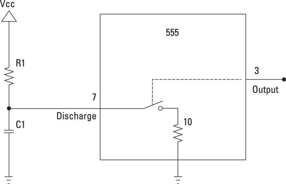
 resistor. This allows the voltage on C1 to discharge through the 555.
 , and C1 is
  . Then, you would calculate the time interval like this:
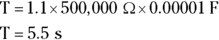


 and the capacitor is
  . Then, the total length of the cycle is calculated like this:
 resistors and a
  capacitor, the output signal will be 48 kHz, and each cycle will last just a few millionths of a second.
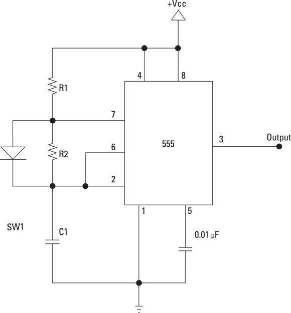
 resistor. When the set switch is depressed, pin 2 is shorted to ground. This
causes the voltage to bypass pin 2, resulting in a momentary low pulse, which triggers the 555. Once triggered, the output pin goes high.
resistor. When the set switch is depressed, pin 2 is shorted to ground. This
causes the voltage to bypass pin 2, resulting in a momentary low pulse, which triggers the 555. Once triggered, the output pin goes high.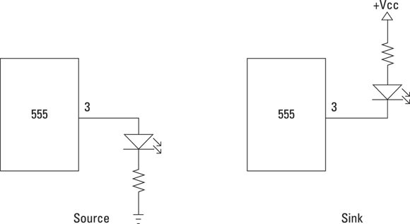
 resistor (brown-black-orange)
 resistor (yellow-violet-brown)
 resistor (yellow-violet-yellow)
 electrolytic capacitor
 ceramic disk capacitor
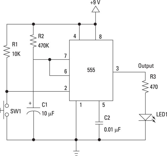


 resistor (brown-black-orange)
 resistors (brown-black-red)
 electrolytic capacitor
 ceramic disk capacitor
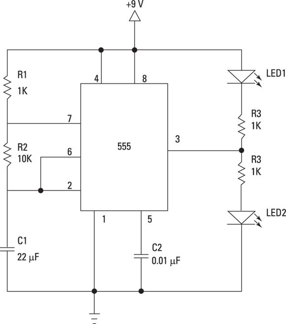


 resistors (brown-black-orange)
 ceramic disk capacitor

 capacitor should be inserted in holes G20 and G21.
 and
and  along with a
  capacitor to produce the 1.5Hz output. The second timer — 555 (2)
— uses
capacitor to produce the 1.5Hz output. The second timer — 555 (2)
— uses  and a
and a  resistors and a
  capacitor to create the output tone. The output of the first timer is sent to the reset of the second timer, and the output of the second timer is sent through a
  capacitor to an
  speaker.
 speaker. If you have an old unamplified computer speaker, you can use it. I recommend you solder 2- to 3-inch lengths of 20-gauge solid wire to the speaker terminals so you can easily connect the speaker to the breadboard.
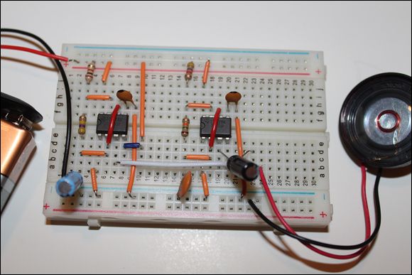
 R3 with a
  resistor, and then add a
  potentiometer in series with the resistor. As you turn the potentiometer, the tone changes.
 potentiometer in series with R1. Then, as you turn the potentiometer, the beeping rate changes.
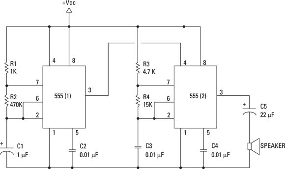
 resistor (brown-black-red)
 resistor (yellow-violet-yellow)
 resistor (yellow-violet-red)
 resistor (brown-green-orange)
 electrolytic capacitor
 electrolytic capacitor
 ceramic disk capacitors


 Electrolytic
 Ceramic Disk
 Ceramic Disk
 Ceramic Disk
 Electrolytic