Introduction
In this chapter, you will learn how to install EAGLE™ Light Edition and will discover the various views and screens that make up an EAGLE project. EAGLE (Easily Applicable Graphical Layout Editor) is a product of the German company Cadsoft. The company is now a subsidiary of Premier Farnell, which also owns Newark Electronics in the United States and CPC in the United Kingdom.
The software has been around for many years, and despite having a user interface that can seem a little daunting to newcomers, it is a powerful and flexible product. It has become a standard for hobby use primarily because of its freeware version and the large set of component libraries and general adoption as the standard tool for open-source hardware (OSH) providers such as Sparkfun and Adafruit. Generally, you will find EAGLE design files available for their OSH products as well as for high-profile products such as the Arduino family of circuit boards.
![]()
Because you are reading this book, you probably want to make a printed circuit board (PCB) and already have a basic understanding of what exactly a PCB is and how it works. However, PCBs come with their own set of jargon, and it is worth establishing exactly what we mean by vias, tracks, pads, and layers.
The main focus of the book will be on making double-sided professional-quality circuit boards. This book assumes that you will design circuit boards and then e-mail the design files to a low-cost PCB fabrication service (as low as US$10 for 10 boards) that will actually make the boards. The making of PCBs at home is now largely redundant because they can generally be made at lower cost and to a better standard than home PCB etching, with all its attendant problems of handling and disposing of toxic chemicals or the need for expensive milling machines.
Figure 1-1 shows the anatomy of a two-layer PCB. You will see exactly how this PCB was designed later in this book, where it is used as an example. For now, let’s briefly explain the anatomy of a PCB. Referring to Figure 1-1, we have the following:
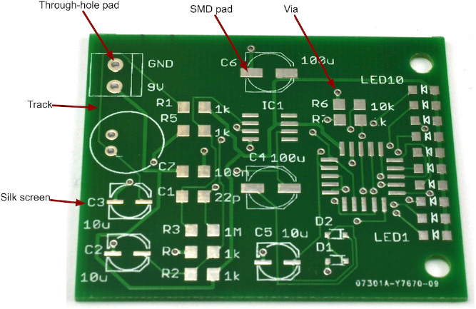
FIGURE 1-1 Anatomy of a double-sided PCB.
• Pads are where the components are soldered to the PCB.
• Tracks are the copper tracks that connect pads together.
• Vias are small holes through the board that link a bottom and top track together electrically. Tracks on the same layer cannot cross, so often, when you are laying out a PCB, you need a signal to jump from one layer to another.
• Silk-screening refers to any lettering that will appear on the final board. It is common to label components and the outline of where they fit so that when it comes to soldering the board together, it is easy to see where everything fits.
• Stop mask is a layer of insulating lacquer that covers both sides of the board except where there are pads.
Pads are either though hole, where components with leads are pushed through from the top, soldered underneath, and then the excess lead snipped off, or surface mount, where the components are soldered to the top of the pad. Figure 1-2 shows a board that contains both surface-mount and through-hole components.
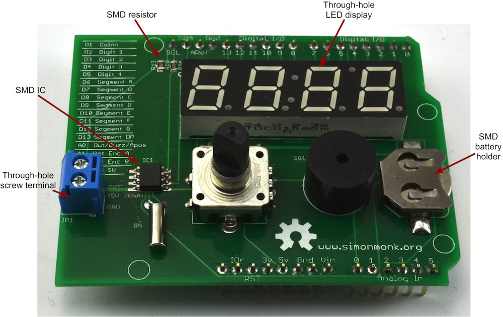
FIGURE 1-2 Through-hole and surface-mount components.
Surface-mount components are often referred to as surface-mount devices (SMDs) and are replacing through-hole components in most commercial products. This is so because SMD components are smaller and cheaper than their through-hole counterparts, and the boards that use them are also easier to make. You will also see the term surface-mount technology (SMT) used.
In commercial surface-mount PCB production, and increasingly for hobbyists, boards are soldered by creating a mask that allows solder paste to be deposited on the pads, then the components are placed precisely on the pads, and then the whole board is baked in an oven that melts the solder paste, soldering the components without the difficulty of soldering each component separately.
SMD ovens are still too expensive for most hobbyists, but many people have had success modifying toaster ovens to operate at the high and precisely controlled temperatures required. Such experiments usually require the safety features of the toaster oven to be disabled and are therefore often referred to as “fire starters” for good reason. However, like so many things in life, with care, common sense, and a watchful eye, such things can be made to work safely.
The choice of surface-mount versus through-hole design is less cut and dried for the hobbyist just wanting to make one or two boards for a specific project. For a single project that is never intended to be made as a commercial product, through-hole design is much simpler to solder by hand. Through-hole component leads are nearly always at least 0.1 in. apart, whereas surface-mount chips can have pins that are just 0.5 mm apart. Although many SMDs are easy enough to solder by hand, many others are just too small.
Figure 1-3 shows a selection of electronic components in both surface-mount and through-hole “flavors.” As you can see, the SMDs are very much smaller than their through-hole equivalents. This generally means that you can get a lot more of them on the same area of a PCB.
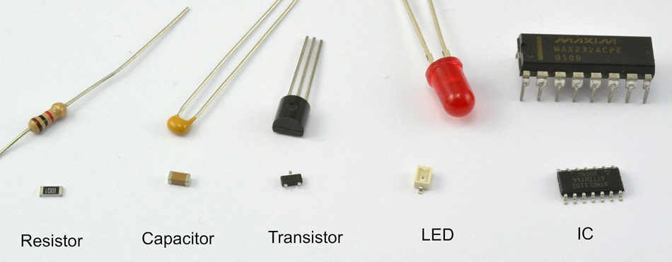
FIGURE 1-3 A selection of through-hole and surface-mount devices.
![]()
Ultimately, if you want to produce something of professional quality, then PCBs are the only way to go. However, while you are prototyping a design, it is a very good idea to test out your design before you start getting PCBs manufactured. Every time you find something wrong with your design and have to get a new batch of PCBs made, you will be increasing costs, both in time and in money. It is far better to get the design as perfect as possible before you commit to a board. This is a bit like writing a book—you wouldn’t print and bind the first draft; you need to be certain that the book is how you want it before you commit to paper.
This is a book about the EAGLE PCB and building PCBs. It is not an electronics primer, so if you need to learn more about electronics in general, then take a look at the books Hacking Electronics and Practical Electronics for Inventors, both from TAB Books.
Assuming that you have a schematic diagram for what you want to build, there are a number of useful construction techniques that you can use to build your prototypes quickly and easily.
Solderless breadboard (Figure 1-4) is very useful for quickly trying out designs before you commit them to solder. You poke the leads of components into the sockets, and metal clips behind the holes connect all the holes on a row together.

FIGURE 1-4 Solderless breadboard.
Breadboard comes in all shapes and sizes, but a big one is probably most useful. The breadboard in Figure 1-4 has 63 rows by 2 columns with two supply strips down each side. It is also mounted on an aluminum base with rubber feet to stop it from moving about on the table. This is a very common size of breadboard, and most suppliers will have something similar.
Figure 1-4b shows how the conductive strips are arranged underneath the plastic top surface of the board. All the holes that share a common gray area beneath are connected together in rows of five connectors. The long strips down each side are used for the power supply to the components, one positive and one negative. They are color-coded red and green.
Breadboards are often modular and will clip together in sections to make as big a board as you need. Figure 1-5 shows an example of a simple breadboard prototype.

FIGURE 1-5 A breadboard prototype.
The main advantage of a solderless breadboard is that it’s, well, solderless. Thus you can quickly and easily change the design just by unplugging components and leads as you need to. The disadvantage is that wires can fall out and leads of components can touch, so a breadboard is only good for the first pass of a prototype. It probably would not be wise to deploy a breadboard-built design for real use. Eventually, something would work loose, and the prototype will stop working. For something more durable as a prototype, there is really no substitute for soldering.
The other disadvantage of breadboard is that the layout is fixed, so components end up very spaced out from each other, often with a large number of jumper wires linking everything together.
Perfboard (perforated board) is one of a number of types of board designed specifically for prototyping. It is made from the same material as a PCB but has no copper on it. It is just a board with an array of holes in it on a 0.1-in. grid (Figure 1-6).

FIGURE 1-6 A perfboard prototype.
Component leads are pushed through from the top and soldered together underneath using either their leads (if they will reach) or lengths of solid-core wire. The perfboard effectively provides a rigid structure to keep the components in position.
A variation on perfboard called protoboard is just like perfboard except that behind each hole is a copper pad. The pads are not connected together, but they serve to hold the components tight to the board. This arrangement does, however, make it more difficult to move a component once it is soldered. Generally, if a design uses dual in-line (DIL) integrated circuits (ICs), then protoboard with solder pads is easier to use than regular perfboard.
The advantage of perfboard and protoboard is that the layout of the components can be closer to the schematic diagram because you are not constrained to using fixed strips of connectors. Such designs can be strong enough to deploy in a project permanently.
Stripboard (Figure 1-7) is a bit like general-purpose PCB. It is a perforated board with conductive strips running underneath, rather like breadboard. The board can be cut to the size you need, and components and wires are soldered onto it.
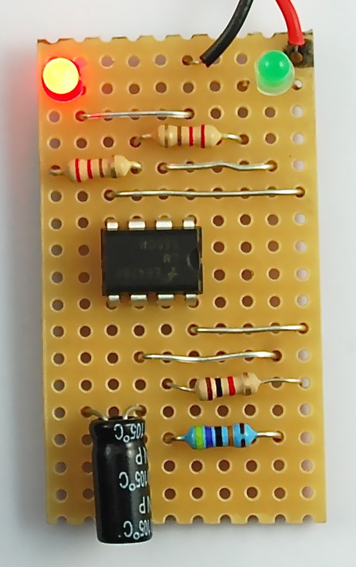
FIGURE 1-7 Stripboard prototype.
As with breadboard, laying out a project on stripboard requires a bit of skill to rearrange the logical layout of the schematic into something that will work with the strips of the stripboard. Figure 1-8 shows the stripboard layout for the prototype in Figure 1-7.

FIGURE 1-8 Stripboard layout.
The X’s underneath the IC are breaks in the track, which are made with a drill bit, and one of the goals of a good stripboard layout is to try to avoid too many breaks having to be made in the track. Breaks are unavoidable for an IC such as this. If we did not make them, pin 1 would be connected to pin 8, pin 2 to pin 7, and so on, and nothing would work.
![]()
Having prototyped your design and being sure that it is time to start making PCBs, let’s get on with installing and configuring EAGLE, the design software that we will use to create PCBs. One of the great things about EAGLE is that it is available for Windows, Mac, and Linux platforms. Thus the first step in installation is to go to www.cadsoftusa.com and click on the “Downloads” button. The instructions are for Version 6.3 of EAGLE.
Select the download for your platform, and then follow the instructions in the section for your operating system below.
For a Windows installation, you will need a machine running Windows XP, Vista, or 7. Download the self-extracting archive (eagle-win-6.3.0.exe), and allow it to run. After the file has been unzipped, the dialog shown in Figure 1-9 will open. Click “Setup” to start the installation process (Figure 1-10).
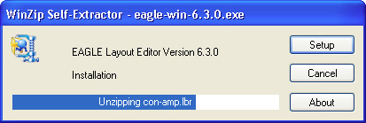
FIGURE 1-9 The EAGLE self-extracting archive.
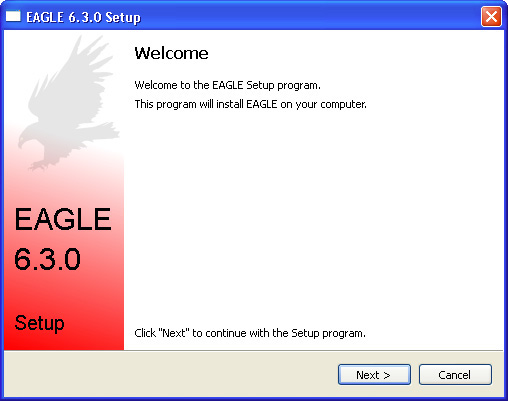
FIGURE 1-10 The EAGLE installer.
You can just accept the defaults most of the way through the installation until you get to the “EAGLE License” step. Here you should select the option “Run as Freeware” (Figure 1-11).
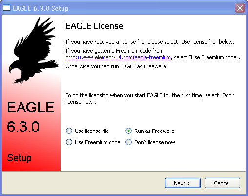
FIGURE 1-11 Installing EAGLE as freeware.
Eventually you will get confirmation that the installation is complete. You will find that the installer has added a new program group to the Start menu from which you can launch EAGLE. You can now skip ahead to the “First Run” section.
When installing on a Mac, EAGLE is distributed as a zipped package installer rather than a disk image. After downloading the file eagle-mac-6.3.0.zip, the file will extract to a package installer eagle-6.3.0.pkg. Double-click it to start the installation process (Figure 1-12).
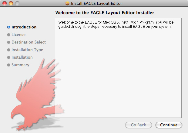
FIGURE 1-12 The Mac installer.
You can accept the default options for the whole installation, but unlike the Windows installation, you will not be prompted to say what kind of license you are using. Instead, this will happen the first time you run the software (Figure 1-13). Select the option “Run as Freeware.”
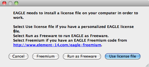
FIGURE 1-13 Selecting license type on first run (Mac).
Having downloaded the installation file for Linux (eagle-lin-6.3.0.run), try running it by opening a terminal session, changing to the “Downloads” directory, and running the following command:
![]()
If you are lucky, the installer will run in a similar fashion to the Windows installer. If you are unlucky, you might see something like Figure 1-14.
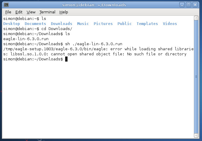
FIGURE 1-14 Installation failure on Linux.
The root cause of this is incompatible versions of two libraries (libssl.so.1.0.0 and libcrypto.so.1.0.0). EAGLE requires 32-bit versions of these libraries, and resolving this problem is not always easy. Useful pointers on this can be found at http://blog.raek.se/2012/01/06/running-cadsoft-eagle-version-6-in-ubuntu-gnulinux/.
![]()
Whatever operating system you are using, launch EAGLE. The following screen shots are all for Windows, but you will find that it looks much the same in Mac and Linux.
The first time you run EAGLE, you will get something like the message shown in Figure 1-15.
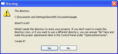
FIGURE 1-15 Confirming creation of a documents folder.
This is asking your permission to create a documents folder into which EAGLE will store the files for the projects that you are working on. You should say “Yes” to this.
If all is well, EAGLE will then open up the EAGLE Control Panel (Figure 1-16).
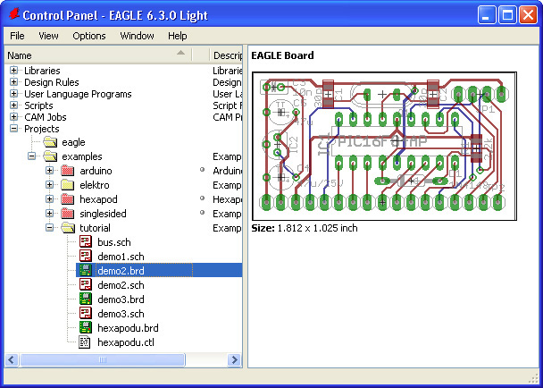
FIGURE 1-16 EAGLE Control Panel.
You will mostly use the Control Panel as a convenient way to access your projects. It also allows you access to all the other different documents that EAGLE uses. These includes
• Libraries of components
• Design rules that specify spacing between tracks and all manner of other things
• User-language programs (You can write your own and download programs to extend EAGLE.)
• Scripts that automate EAGLE activities
• CAM (computer-aided manufacturing) jobs that specify how the EAGLE design is converted into files suitable for PCB fabrication
![]()
Within a project, the two main files you will be using are the schematic file, which will have the extension .sch, and the board layout file, which will have the extension .brd.
Navigate down the folders in “Projects” to demo2.brd, as shown in Figure 1-16, and then double-click both demo2.brd and demo2.sch to open both the board layout and the schematic (Figure 1-17). Later on, when you are working on a project, you will need to make sure that the schematic and board files are open for the project, or they can become out of step, leading to all sorts of problems.
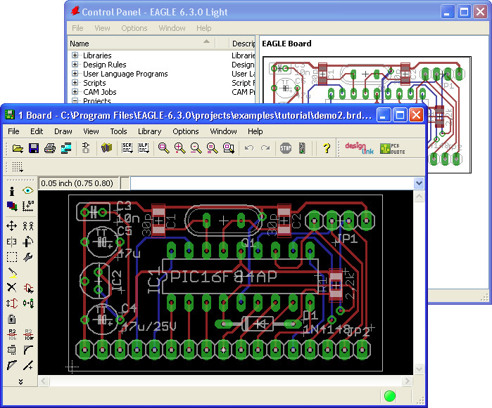
FIGURE 1-17 Example board and schematic files.
![]()
As part of the process of setting up our environment, we will download some useful things from the Internet that will just help to get us started and make EAGLE that much easier to use.
You are going to load up two libraries of parts, one from Sparkfun and one from Adafruit. Although EAGLE comes with a huge collection of parts organized into libraries, the collection of parts is so huge that it can be very difficult to “see the wood for the trees” and find the part that you want. However, the Adafruit and Sparkfun libraries offer simplified lists of the most common components, and of course, they include components that the companies sell.
To download the Sparkfun library, navigate to https://github.com/sparkfun/SparkFun-Eagle-Libraries with your browser, and select the option to download a zip file (the icon looks like a cloud with an arrow pointing down).
Once the zip file has downloaded, the .lbr files that it contains all need to be extracted into the .lbr folder inside your EAGLE installation folder (Figures 1-18 and 1-19).

FIGURE 1-18 EAGLE .lbr folder.
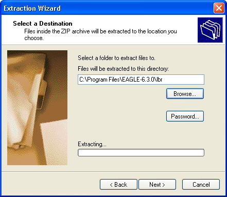
FIGURE 1-19 Extracting files straight into the EAGLE .lbr folder.
This will add about 17 .lbr files from LilyPad-Wearables.lbr to SparkFun-Sensors.lbr to the .lbr directory. You can remove the README file once it has been unzipped.
The installation for the Adafruit is a similar process. First navigate to http://github.com/adafruit/Adafruit-Eagle-Library and again download using the zip option and unzip the contents in the same way as you did the Sparkfun library. However, the Adafruit parts are all contained in a single library rather than a collection. Thus you can, if you wish, just add the single .lbr file rather than contain it in a folder.
To check that both sets of libraries have been installed, go back to your EAGLE Control Panel and expand the “Libraries” tab. You should see a list something like Figure 1-20.
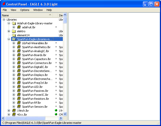
FIGURE 1-20 Sparkfun and Adafruit libraries installed.
Design rules specify all sorts of things about the design, the gaps between pads and tracks, and other things like that. Sparkfun has put together a useful default set of design rules that we will use in this book, so it makes sense to install them now so that you can use them in any of the EAGLE projects you create.
The Sparkfun design rules can be downloaded from the Sparkfun site at www.sparkfun.com/tutorials/115. They are contained in a single .drc file. You can right-click on this file on the web page and chose “Save As” to directly save it into the drc folder within your EAGLE installation.
This book develops a number of example EAGLE projects. You will find it useful to download these so that you can open them up and take a look at them from within the EAGLE software. These files can be downloaded from www.simonmonk.org. Just follow the link to this book.
![]()
The developers of EAGLE have to make some money somewhere, and professionals will soon find that they need features of EAGLE that are not available in the light edition. However, for most of us, the Light edition will do just fine.
There are no restrictions on the number of projects you can design using the software. The main restrictions of the light edition include the following:
• The maximum size of a board that you can design with this edition is 4 × 3.2 in. (100 × 80 mm). This may not sound very big, but actually you can fit a lot of components in an area of that size. Also, because the PCB fabrication services tend to get expensive as boards get bigger, it is no bad thing to keep your designs compact.
• A maximum of two layers is allowed. This means that you can have copper tracks on the top of the board and on the bottom of the board, but you cannot produce four-layer (or more) boards. Again, this is not a problem for hobby use.
• You can only create one sheet on the Schematic Editor. When designing a circuit, electronics engineers will often split a complex design into a number of schematic diagrams with links from one sheet to another. This restriction means that you have to fit all your design onto a single schematic diagram. This is nowhere near as restrictive as it might sound because there is no practical limit to how big that sheet can be.
EAGLE Light can be used as freeware as long as the use is noncommercial or for nonprofit applications. If you plan to build a business out of a product that you design with EAGLE Light, then you should buy a commercial license. For EAGLE Light, this is only $70 at the time of this writing.
![]()
In this chapter you have learned a little about PCBs, installed EAGLE, and run it for the first time. You can now move on to Chapter 2, where you can start designing a simple project using EAGLE.