
The material in this chapter is similar to that in Chap. 4. Here, however, the analysis techniques apply to ac phasor-domain circuits instead of to dc resistive circuits and so to voltage and current phasors instead of to voltages and currents and to impedances and admittances instead of just to resistances and conductances. Also, an analysis is often considered completed after the unknown voltage or current phasors are determined. The final step of finding the actual time-function voltages and currents is often not done because they are not usually important. Besides, it is a simple matter to obtain them from the phasors.
One other introductory note: From this point on, the term “impedance” and “admittances” will often be used to mean components with impedances and components with admittances, as is common practice.
As has been explained, mesh and loop analyses are usually easier to do with all current sources transformed to voltage sources and nodal analysis is usually easier to do with all voltage sources transformed to current sources. Figure 13-1a shows the rather obvious transformation from a voltage source to a current source, and Fig. 13-1b shows the transformation from a current source to a voltage source. In each circuit the rectangle next to Z indicates components that have a total impedance of Z. These components can be in any configuration and can, of course, include dependent sources—but not independent sources.
Fig. 13-1
Mesh analysis for phasor-domain circuits should be apparent from the presentation of mesh analysis for dc circuits in Chap. 4. Preferably all current sources are transformed to voltage sources, then clockwise-referenced mesh currents are assigned, and finally KVL is applied to each mesh.
As an illustration, consider the phasor-domain circuit shown in Fig. 13-2. The KVL equation for mesh 1 is

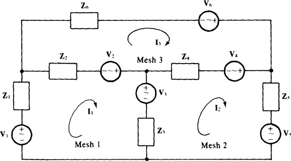
Fig. 13-2
where I1 Z1, (I1 — I3)Z2, and (I1 — I2)Z3 are the voltage drops across the impedances Z1(Z2, and Z3. Of course, V1 + V2 — V3 is the sum of the voltage rises from voltage sources in mesh 1. As a memory aid, a source voltage is added if it “aids” current flow—that is, if the principal current has a direction out of the positive terminal of the source. Otherwise, the source voltage is subtracted.
This equation simplifies to

The Z1 + Z2 + Z3 coefficient of I1 is the self-impedance of mesh 1, which is the sum of the impedances of mesh 1. The — Z3 coefficient of I2 is the negative of the impedance in the branch common to meshes 1 and 2. This impedance Z3 is a mutual impedance —it is mutual to meshes 1 and 2. Likewise, the — Z2 coefficient of I3 is the negative of the impedance in the branch mutual to meshes 1 and 3, and so Z2 is also a mutual impedance. It is important to remember in mesh analysis that the mutual terms have initial negative signs.
It is, of course, easier to write mesh equations using self-impedances and mutual impedances than it is to directly apply KVL. Doing this for meshes 2 and 3 results in


and
Placing the equations together shows the symmetry of the I coefficients about the principal diagonal:
Usually, there is no such symmetry if the corresponding circuit has dependent sources. Also, some of the off-diagonal coefficients may not have initial negative signs.
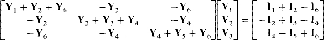
This symmetry of the coefficients is even better seen with the equations written in matrix form:
For some scientific calculators, it is best to put the equations in this form and then key in the coefficients and constants so that the calculator can be used to solve the equations. The calculator-matrix method is generally superior to any other procedure such as Cramer’s rule.
Loop analysis is similar except that the paths around which KVL is applied are not necessarily meshes, and the loop currents may not all be referenced clockwise. So, even if a circuit has no dependent sources, some of the mutual impedance coefficients may not have initial negative signs. Preferably, the loop current paths are selected such that each current source has just one loop current through it. Then, these loop currents become known quantities with the result that it is unnecessary to write KVL equations for the loops or to transform any current sources to voltage sources. Finally, the required number of loop currents is B — N + 1 where B is the number of branches and N is the number of nodes. For a planar circuit, which is a circuit that can be drawn on a flat surface with no wires crossing, this number of loop currents is the same as the number of meshes.
Nodal analysis for phasor-domain circuits is similar to nodal analysis for dc circuits. Preferably, all voltage sources are transformed to current sources. Then, a reference node is selected and all other nodes are referenced positive in potential with respect to this reference node. Finally, KCL is applied to each nonreference node. Often the polarity signs for the node voltages are not shown because of the convention to reference these voltages positive with respect to the reference node.
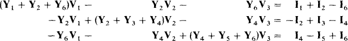
For an illustration of nodal analysis applied to a phasor-domain circuit, consider the circuit shown in Fig. 13-3. The KCL equation for node 1 is

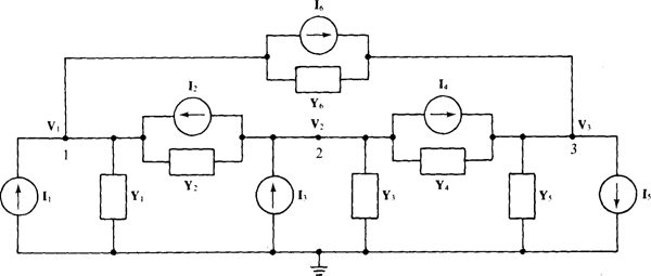
Fig. 13-3
where V1, Y1,(V1 — V2)Y2, and (V1 — V3)Y6 are the currents flowing away from node 1 through the admittances Y1, Y2, and Y6. Of course, I1, + I2 — I6 is the sum of the currents flowing into node 1 from current sources,
This equation simplifies to

The coefficient Y1 + Y2 + Y6 of V1, is the self-admittance of node 1, which is the sum of the admittances connected to node 1. The coefficient — Y2 of V2 is the negative of the admittance connected between nodes 1 and 2. So, Y2 is a mutual admittance. Similarly, the coefficient — Y6 of V3 is the negative of the admittance connected between nodes 1 and 3, and so Y6 is also a mutual admittance.
It is, of course, easier to write nodal equations using self-admittances and mutual admittances than it is to directly apply KCL. Doing this for nodes 2 and 3 produces

and

Usually, there is no such symmetry if the corresponding circuit has dependent sources. Also, some of the off-diagonal coefficients may not have initial negative signs. In matrix form these equations are
The use of PSpice to analyze an ac circuit is perhaps best introduced by way of an illustration. Consider the time-domain circuit of Fig. 13-4. A suitable PSpice circuit file for obtaining V0 and I„ is
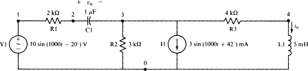
Fig. 13-4
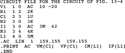
Observe that the resistor, inductor, and capacitor statements are essentially the same as for the other types of analyses, except that no initial conditions are specified in the inductor and capacitor statements. If the circuit had contained a dependent source, the corresponding statement would have been the same also.
In the independent source statement, the term AC, which must be included after the node specification, is followed by the peak value of the sinusoidal source and then the phase angle. If rms magnitudes are desired in the printed outputs, then rms values instead of peak values, should be specified in the independent source statement.
The frequency of the sources (and all sources must have the same frequency), in hertz, is specified in an. AC control statement, after.AC LIN 1. Here the frequency is 1000/2π = 159.155 Hz. (The source frequency of 1000 is, of course, in radians per second.) Note that this frequency must be specified twice. The format of the. AC control statement allows for the variation in frequency, a feature that is not used in this example.
If this circuit file is run with PSpice, the output file will include the following:
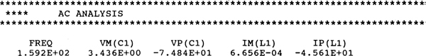
Consequently, 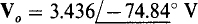 , and
, and 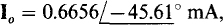 where the magnitudes are expressed in peak values. As stated, if rms magnitudes are desired, then rms magnitudes should be specified in the independent source statements.
13.1 Perform a source transformation on the circuit shown in Fig. 13-5.
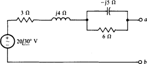
Fig. 13-5
The series impedance is 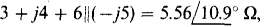 which when divided into the voltage of the original source gives the source current of the equivalent circuit:
As shown in Fig. 13-6, the current direction is toward node a, as it must be because the positive terminal of the voltage source is toward that node also. The parallel impedance is, of course, the series impedance of the original circuit.
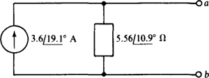
Fig. 13-6
13.2 Perform a source transformation on the circuit shown in Fig. 13-7.
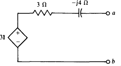
Fig. 13-7
This circuit has a dependent voltage source that provides a voltage in volts that is three times the current I flowing elsewhere (not shown) in the complete circuit. When, as here, the controlling quantity is not in the circuit being transformed, the transformation is the same as for a circuit with an independent source. Therefore, the parallel impedance is 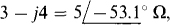 and the source current directed toward node a is
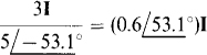
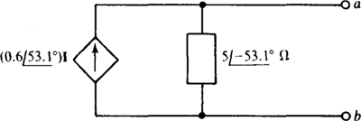
Fig. 13-8
When the controlling quantity is in the portion of the circuit being transformed, a different method must be used, as is explained in Chap. 14 in the section on Thévenin’s and Norton’s theorems.
13.3 Perform a source transformation on the circuit shown in Fig. 13-9.
Fig. 13-9
The parallel impedance is 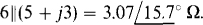 The product of the parallel impedance and the current is the voltage of the equivalent voltage source:

As shown in Fig. 13-10, the positive terminal of the voltage source is toward node a, as it must be since the current of the original circuit is toward that node also. The source impedance is, of course, the same 3.07/15.7° Ω, but is in series with the source instead of in parallel with it.

Fig. 13-10
13.4 Perform a source transformation on the circuit shown in Fig. 13-11.
Fig. 13-11
This circuit has a dependent current source that provides a current flow in amperes that is six times the voltage V across a component elsewhere (not shown) in the complete circuit. Since the controlling quantity is not in the circuit being transformed, the transformation is the same as for a circuit with an independent source. Consequently, the series impedance is  and the source voltage is

with, as shown in Fig. 13-12, the positive polarity toward node a because the current of the current source is also toward that node. The same source impedance is, of course, in the circuit, but is in series with the source instead of in parallel with it.
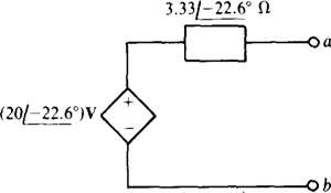
Fig. 13-12
13.5 Assume that the following equations are mesh equations for a circuit that does not have any current sources or dependent sources. Find the quantities that go in the blanks.
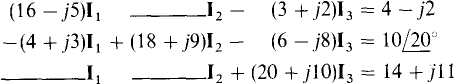
The key is the required symmetry of the I coefficients about the principal diagonal. Because of this symmetry, the coefficient of I2 in the first equation must be —(4 + j3), the same as the coefficient of I1, in the second equation. Also, the coefficient of I1, in the third equation must be —(3 + j2), the same as the coefficient of I3 in the first equation. And the coefficient of I2 in the third equation must be —(6 — j8), the same as the coefficient of I3 in the second equation.
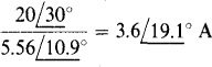
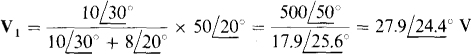
13.6 Find the voltages across the impedances in the circuit shown in Fig. 13-13a. Then transform the voltage source and  component to an equivalent current source and again find the voltages. Compare results.
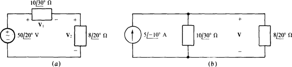
Fig. 13-13
By voltage division,
By KVL,

Transformation of the voltage source results in a current source of 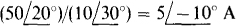 A in parallel with a
  component, both in parallel with the
  component, as shown in Fig. 13-13b. In this parallel circuit, the same voltage V is across all three components. That voltage can be found from the product of the total impedance and the current:
13.7 Find the mesh currents for the circuit shown in Fig. 13-14.
Fig. 13-14
The self-impedance and mutual-impedance approach is almost always best for getting mesh equations. The self-impedance of mesh 1 is 4 + j15 + 6 — j7 = 10 + j8 Ω, and the impedance mutual with mesh 2 is 6 —j7Ω. The sum of the source voltage rises in the direction of I1 is 
 In this sum the
  voltage is subtracted because it is a voltage drop instead of a rise. The mesh 1 equation has, of course, a left-hand side that is the product of the self-impedance and I, minus the product of the mutual impedance and I2. The right-hand side is the sum of the source voltage rises. Thus, this equation is

No KVL equation is needed for mesh 2 because I2 is the only mesh current through the  current source. As a result,
  The initial negative sign is required because I2 has a positive direction down through the source, but the specified
  current is up. Remember that, if for some reason a KVL equation for mesh 2 is wanted, a variable must be included for the voltage across the current source since this voltage is not known.
The substitution of  into the mesh 1 equation produces

from which

Another good analysis approach is to first transform the current source and parallel impedance to an equivalent voltage source and series impedance, and then find II from the resulting single mesh circuit. If this is done, the equation for I1 will be identical to the one above.
13.8 Solve for the mesh currents I1 and I2 in the circuit shown in Fig. 13-15.
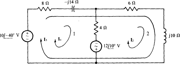
Fig. 13-15
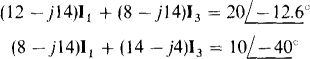
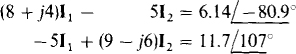
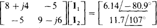
The self-impedance and mutual-impedance approach is the best for mesh analysis. The self-impedance of mesh 1 is 8 — j14 + 4 = 12 — j14 Ω, the mutual impedance with mesh 2 is 4 Ω, and the sum of the source voltage rises in the direction of I1, is  So, the mesh 1 KVL equation is

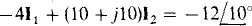
For mesh 2 the self-impedance is 6 + j10 + 4 = 10 + j Ω, the mutual impedance is 4Ω, and the sum of the voltage rises from voltage sources is  So, the mesh 2 KVL equation is
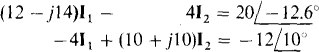
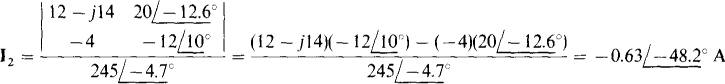
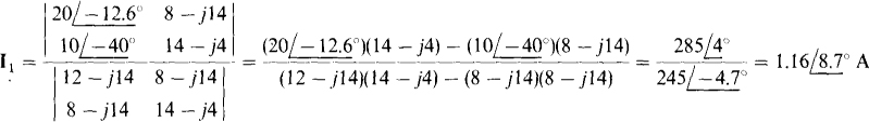
By Cramer’s rule,
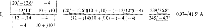
and since I2 has the same denominator as I1,
13.9 Use loop analysis to find the current down through the 4-Ω resistor in the circuit shown in Fig. 13-15.
The preferable selection of loop currents is I1, and I3 because then I1 is the desired current since it is the only current in the 4-Ωresistor and has a downward direction. Of course, the self-impedance and mutual-impedance approach should be used.
The self-impedance of the I1, loop is 8 — j14 + 4 = 12 — j14 Ω, the mutual impedance with the I3 loop is 8 — j14Ω, and the sum of the source voltage rises in the direction of I1, is 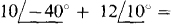
 The self-impedance of the I3 loop is 8-j14 + 6 + j10 = 14 — j4Ω, of which 8 j14Ω is mutual with the I1, loop. The source voltage rise in the direction of I3 is
  Therefore, the loop equations are
The mutual terms are positive because the I1 and I3 loop currents have the same direction through the mutual impedance.
By Cramer’s rule,
As a check, notice that this loop current should be equal to the difference in the mesh currents I1 and I2 found in the solution to Prob. 13.8. It is, since 
13.10 Find the mesh currents for the circuit shown in Fig. 13-l6a.
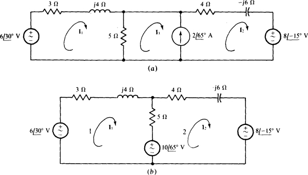
Fig. 13-16
A good first step is to transform the  current source and parallel 5-Ω resistor into a voltage source and series resistor, as shown in the circuit of Fig. 13-16b. Note that this transformation eliminates mesh 3. The self-impedance of mesh 1 is 3 + j4 + 5 = 8 + j4 Ω, and that of mesh 2 is 4 — j6 + 5 = 9 — j6Ω. The mutual impedance’ is 5Ω. The sum of the voltage rises from sources is
 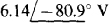 for mesh 1 and
 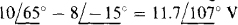 for mesh 2. The corresponding mesh equations are
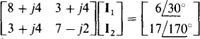
In matrix form these are
These equations are best solved using a scientific calculator (or a computer). The solutions obtained are  and
and 
From the original circuit shown in Fig. 13-16a, the current in the current source is 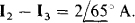 Consequently,

13.11 Use loop analysis to solve for the current flowing down through the 5-Ω resistor in the circuit shown in Fig. 13-16a.
Because this circuit has three meshes, the analysis requires three loop currents. The loops can be selected as in Fig. 13-17 with only one current I1 flowing through the 5-Ω resistor so that only one current needs to be solved for. Also, preferably only one loop current should flow through the current source.
Fig. 13-17
The self-impedance of the I1 loop is 3 + j4 + 5 = 8 + j4Ω, the impedance mutual with the I2 loop is 3 + j4Ω, and the aiding source voltage is  V. So, the loop 1 equation is

The I2 coefficient is positive because I2 and I1 have the same direction through the mutual components.
For the second loop, the self-impedance is 3 + j4 + 4j2Ω, of which 3 + j4Ω is mutual with loop 1. The current flowing through the components of 4 — j6Ω produces a voltage drop of 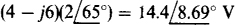 that has the same effect as the voltage from an opposing voltage source. In addition, the voltage sources have a net aiding voltage of
  The resulting loop 2 equation is

In matrix form these equations are
A scientific calculator can be used to obtain  from these equations.
As a check, this loop current I1 should be equal to the difference in the mesh currents l1 and I3 found in the solution to Prob. 13.10. It is, since 
13.12 Use mesh analysis to solve for the currents in the circuit of Fig. 13-18.
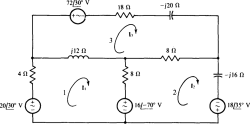
Fig. 13-18
The self-impedances are 4 + j12 + 8 = 12 + j12Ω for mesh 1, 8 + 8 — j16 = 16 — j16Ω for mesh 2, and 18 — j20 + 8 + j12 = 26 — j8Ω for meshes 3. The mutual impedances are 8Ω for meshes 1 and 2, 8Ω for meshes 2 and 3, and jl2Ω for meshes 1 and 3. The sum of the aiding source voltages is 
 for mesh 1,
  for mesh 2, and
  for mesh 3. In matrix form, the mesh equations are
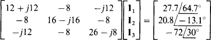
The solutions, which are best obtained by using a calculator or computer, are

13.13 Show a circuit that corresponds to the following mesh equations:
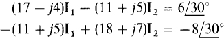
Because there are two equations, the circuit has two meshes: mesh 1 for which I1, is the principal mesh current, and mesh 2 for which I2 is the principal mesh current. The —(11 + j5) coefficients indicate that meshes 1 and 2 have a mutual impedance of 11 + j5Ω which could be from an 11-Ω resistor in series with an inductor that has a reactance of 5Ω. In the first equation the I1 coefficient indicates that the resistors in mesh 1 have a total resistance of 17Ω. Since 11Ω of this is in the mutual impedance, there is 17 — 11 = 6Ω of resistance in mesh 1 that is not mutual. The —j4 of the I1 coefficient indicates that mesh 1 has a total reactance of — 4Ω. Since the mutual branch has a reactance of 5Ω, the remainder of mesh 1 must have a reactance of —4 — 5 = —9Ω, which can be from a single capacitor. The on the right-hand side of the mesh 1 equation is the result of a total of V of voltage source rises (aiding source voltages). One way to obtain this is with a single sourse V that is not in the mutual branch and that has a polarity such that l1 flows out of its positive terminal
Similarly, from the second equation, mesh 2 has a nonmutual resistance of 18 — 11 = 7Ω that can be from a resistor that is not in the mutual branch. And from the j7 part of the I2 coefficient, mesh 2 has a total reactance of 7Ω. Since 5Ω of this is in the mutual branch, there is 7 — 5 = 2Ω remaining that could be from a single inductor that is not in the mutual branch. The —  on the right-hand side is the result of a total of V of voltage source drops—opposing source voltages. One way to obtain this is with a single source of V that is not in the mutual branch and that has a polarity such that I2 flows into its positive terminal
Figure 13-19 shows the corresponding circuit. This is just one of an infinite number of circuits from which the equations could have been written.
Fig. 13-19
13.14 Use loop analysis to solve for the current flowing to the right through the 6-Ω resistor in the circuit shown in Fig. 13-20.
Fig. 13-20
Three loop currents are required because the circuit has three meshes. Only one of the loop currents should flow through the 6-Ω resistor so that only one current has to be solved for. This current is I2, as shown. The paths for the two other loop currents can be selected as shown, but there are other suitable paths.
It is relatively easy to put these equations into matrix form. The loop self-impedances and mutual impedances can be used to fill in the coefficient matrix. And the elements for the source vector are  for loop 1 and 0 V for the two other loops. Thus, the equations in matrix form are
The solutions, which are best obtained from a calculator or computer, include 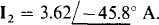
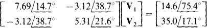
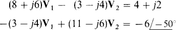
13.15 Solve for the node voltages in the circuit shown in Fig. 13-21.
Fig. 3-21
Using self-admittances and mutual admittances is almost always best for obtaining the nodal equations. The self-admittance of node 1 is
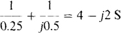
of which 4 S is mutual conductance. The sum of the currents from current sources into node 1 is  A. So, the node 1 KCL equation is

No KCL equation is needed for node 2 because a grounded voltage source is connected to it, making 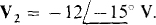 If, however, for some reason a KCL equation is wanted for node 2, a variable has to be introduced for the current through the voltage source because this current is unknown. Note that, because the voltage source does not have a series impedance, it cannot be transformed to a current source with the source transformation techniques presented in this chapter.
The substitution of V2 = —12/—15° into the node 1 equation results in

from which

13.16 Find the node voltages in the circuit shown in Fig. 13-22.
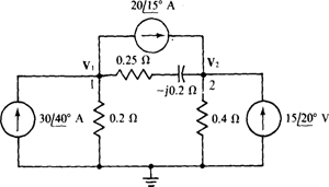
Fig. 13-22
The self-admittance of node 1 is
of which  is mutual admittance. The sum of the currents into node 1 from current sources is
  Therefore, the node 1 KCL equation is

The self-admittance of node 2 is
of which  is mutual admittance. The sum of the currents into node 2 from current sources is
  The result is a node 2 KCL equation of

In matrix form these equations are
The solutions, which are easily obtained with a scientific calculator, are V1 =  and V2 =
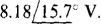
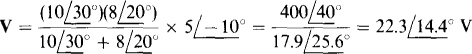
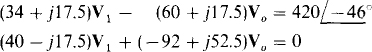
13.17 Use nodal analysis to find V for the circuit shown in Fig. 13-23.
Fig. 13-23
Although a good approach is to transform both voltage sources to current sources, this transformation is not essential because both voltage sources are grounded. (Actually, source transformations are never absolutely necessary.) Leaving the circuit as it stands and summing currents away from the V node in the form of voltages divided by impedances gives the equation of
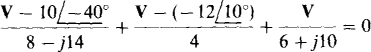
The first term is the current flowing to the left through the 8 — jl4Ω components, the second is the current flowing down through the 4-Ω resistor, and the third is the current flowing to the right through the 6 + j10Ω components.
This equation simplifies to

Further simplification reduces the equation to

from which
Incidentally, this result can be checked since the circuit shown in Fig. 13-23 is the same as that shown in Fig. 13-15 for which, in the solution to Prob. 13.9, the current down through the 4-Ω resistor was found to be  . The voltage V across the center branch can be calculated from this current: V =
  which checks.
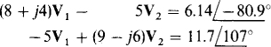
13.18 Find the node voltages in the circuit shown in Fig. 13-24a.
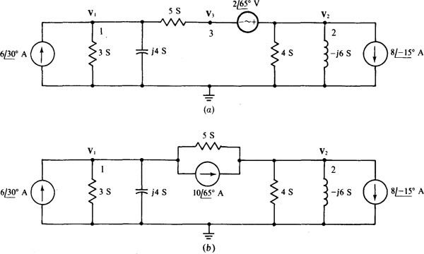
Fig. 13-24
Since the voltage source does not have a grounded terminal, a good first step for nodal analysis is to transform this source and the series resistor to a current source and parallel resistor, as shown in Fig. 13-24b. Note that this transformation eliminates node 3. In the circuit shown in Fig. 13-24b, the self-admittance of node 1 is 3 + j4 + 5 = 8 + j4 S, and that of node 2 is 5 + 4 — j6 = 9 — j6 S. The mutual admittance is 5 S. The sum of the currents into node 1 from current sources is  , and that into node 2 is
  . Thus, the corresponding nodal equations are
Except for having V’s instead of I’s, these are the same equations as for Prob. 13.10. Consequently, the answers are numerically the same: 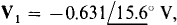 and
and 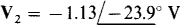 .
.
From the original circuit shown in Fig. 13-24a, the voltage at node 3 is  more negative than the voltage at node 2. So,

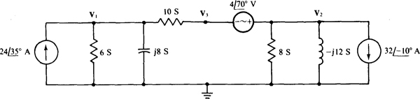
13.19 Calculate the node voltages in the circuit of Fig. 13-25.
Fig. 13-25
The self-admittances are 4 + 8 + j12 = 12 + j12 S for node 1, 8 — jl6 + 8 = 16 — j16 S for node 2, and 8 + 18 — j20 + jl2 = 26 — j8 S for node 3. The mutual admittances are 8 S for nodes 1 and 2, jl2 S for nodes 1 and 3, and 8 S for nodes 2 and 3. The currents flowing into the nodes from current sources are  for node 1,
  for node 2, and
  for node 3. So, the nodal equations are
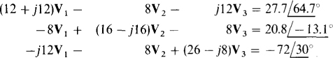
Except for having V’s instead of I’s, this set of equations is the same as that for Prob. 13.12. So, the answers are numerically the same:  , and
, and 
13.20 Show a circuit corresponding to the nodal equations
Since there are two equations, the circuit has three nodes, one of which is the ground or reference node, and the others of which are nodes 1 and 2. The circuit admittances can be found by starting with the mutual admittance. From the —(3 — j4) coefficients, nodes 1 and 2 have a mutual admittance of 3 — j4 S, which can be from a resistor and inductor connected in parallel between nodes 1 and 2. The 8 + j6 coefficient of V, in the first equation is the self-admittance of node 1. Since 3 — j4 S of this is in mutual admittance, there must be components connected between node 1 and ground that have a total of 8 + j6 — (3 — j4) = 5 + j10S of admittance. This can be from a resistor and parallel capacitor. Similarly, from the second equation, components connected between node 2 and ground have a total admittance of 11 — j6— (3 — j4) = 8 — j2 S. This can be from a resistor and parallel inductor.
The 4 + j2 on the right-hand side of the first equation can be from a total current of 4 + j2 =  entering node 1 from current sources. The easiest way to obtain this is with a single current source connected between node 1 and ground with the source arrow directed into node 1. Similarly, from the second equation, the
  can be from a single current source of
  A connected between node 2 and ground with the source arrow directed away from node 2 because of the initial negative sign in .
The resulting circuit is shown in Fig. 13-26.
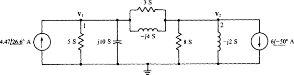
Fig. 13-26
13.21 For the circuit shown in Fig. 13-27, which contains a transistor model, first find V as a function of I. Then, find V as a numerical value.
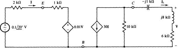
Fig. 13-27
In the right-hand section of the circuit, the current IL is, by current division.

And, by Ohm’s law,

which shows that the magnitude of V is 17.2 × 10⁴ times that of I, and the angle of V is 29.5° — 180° = —150.5° plus that of I. (The — 180° is from the negative sign.)
If this value of V is used in the 0.01-V expression of the dependent source in the left-hand section of the circuit, and then KVL applied, the result is

from which

This, substituted into the equation for V, gives

13.22 Solve for I in the circuit shown in Fig. 13-28.
Fig. 13-28
What analysis method is best for this circuit? A brief consideration of the circuit shows that two equations are necessary whether mesh, loop, or nodal analysis is used. Arbitrarily, nodal analysis will be used to find V1, and then I will be found from V1. For nodal analysis, the voltage source and series resistor are preferably transformed to a current source with parallel resistor. The current source has a current of 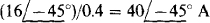 directed into node 1, and the parallel resistor has a resistance of 0.4 Ω.
The self-admittances are
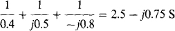
for node 1, and
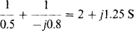
for node 2. The mutual admittance is l/(—j0.8) =j1.25 S.
The controlling current I in terms of V1 is I = V1/j0.5 = –j2Vl, which means that 2I = –j4V1 is thecurrent into node 2 from the dependent current source.
From the admittances and the source currents, the nodal equations are
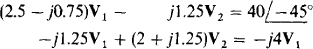
which, with j4V1 added to both sides of the second equation, simplify to
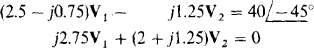
The lack of symmetry of the coefficients about the principal diagonal and the lack of an initial negative sign for the V1 term in the second equation are caused by the action of the dependent source.
If a calculator is used to solve for V1, the result is 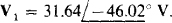 Finally,
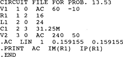
13.23 Use PSpice to obtain the mesh currents in the circuit of Fig. 13-18 of Prob. 13.12.
The first step is to obtain a corresponding PSpice circuit. Since no frequency is specified in Prob. 13.12 (or even if one was), a convenient frequency can be assumed and then used in calculating the inductances and capacitances from the specified inductive and capacitive impedances. Usually, ω = 1 rad/s is the most convenient. For this frequency, the inductor that has an impedance of j12 í has an inductance of 12/1 = 12 H. The capacitor that has an impedance of —j20 Ω has a capacitance of 1/20 = 0.05 F, as should be apparent. And the capacitor that has an impedance of —j16 has a capacitance of 1/16 = 0.0625 F.
Figure 13-29 shows the corresponding PSpice circuit. For convenience, the voltage-source voltages remain specified in phasor form, and the mesh currents are shown as phasor variables. Thus, Fig. 13-29 is really a mixture of a time-domain and phasor-domain circuit diagram.
Fig. 13-29
In the circuit file the frequency must be specified in hertz, which for 1 rad/s is 1/2π = 0.159 155 Hz. The circuit file corresponding to the PSpice circuit of Fig. 13-29 is as follows:
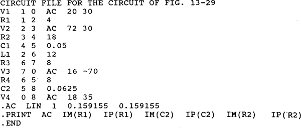
When this circuit file is run with PSpice, the output file will contain the folio wing results.
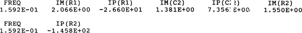
The answers  and
and 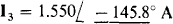 agree within three significant digits with the answers to Prob. 13.12.
13.24 Calculate Vo in the circuit of Fig. 13-30.
By nodal analysis,

Also
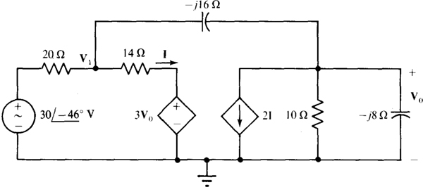
Substituting, from the third equation into the second and multiplying both resulting equations by 280 gives

Use of Crameer’s rule or a scientific calculator provides the solution 
13.25 Repeat Prob. 13.24 using PSpice.
For a PSpice circuit file, capacitances are required instead of the capacitive impedances that are specified i, n the circuit of Fig. 13-30. It is often convenient to assume a frequency of ω = 1 rad/s to obtain these capacitances. Then, of course, f = 1/2π = 0.159 155 Hz is the frequency that must be specified in the circuit file. For ω = 1 rad/s, the capacitor that has an impedance of —j8 Ω has a capacitance of 1/16 = 0.O625 F, and the capacitor that has an impedance of — j8 Ω has a capacitance of 1/8 = 0.125 F. Figure 13-31 shows the PSpice circuit that corresponds to the phasor-domain circuit of Fig. 13-30. The V2 dummy source is required to obtain the controlling current for the Fl current-controlled current source.
Fig. 13-31
The corresponding circuit file is
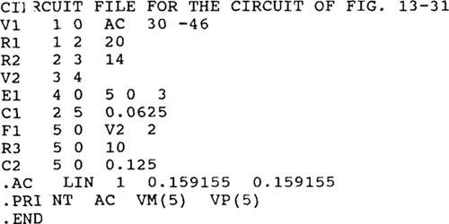
When this circuit file is run with PSpice, the output file includes

from which  which is in complete agreement with the answer to Prob. 13.24.
13.26 Use PSpice to determine v0 in the circuit of Fig. 12-25a of Prob. 12.47.
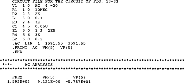
Figure 13-32 is the PSpice circuit corresponding to the circuit of Fig. 12-25a. The op amp has been deleted and a voltage-controlled voltage source El inserted at what was the op-amp output. This source is, of course, a model for the op amp. Also, a large resistor R1 has been inserted from node 1 to node 0 to satisfy the PSpice requirement for at least two components connected to each node.
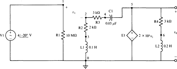
Fig. 13-32
Following is the circuit file. The specified frequency, 1591.55 Hz, is equal to the source frequency of 10 000 rad/s divided by 2π. Also shown is the output obtained when this circuit file is run with PSpice. The answer of 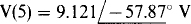 is the phasor for

which agrees within three significant digits with the v0 answer of Prob. 12.47.
13.27 Find V0 in the circuit of Fig. 13-33.

Fig. 13-33
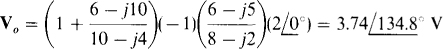
Since the first op-amp circuit has the configuration of a noninverting amplifier, and the second has that of an inverter, the pertinent formulas from Chap. 6 apply, with the R’s replaced by Z’s. So, with the impedances expressed in kilohms,
13.28 Repeat Prob. 13.27 using PSpice.
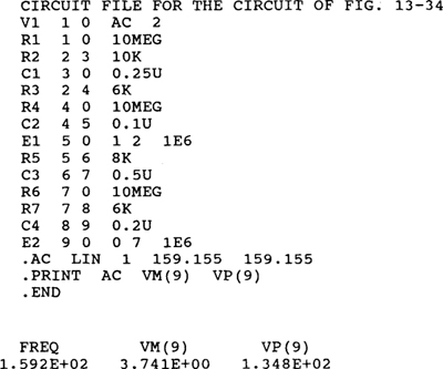
Figure 13-34 is the PSpice circuit corresponding to the circuit of Fig. 13-33, with the op amps replaced by voltage-controlled voltage sources that are connected across the former op-amp output terminals. In addition, a large resistor Rl has been inserted from node 1 to node 0 to satisfy the PSpice requirement for at least two components connected to each node. The large resistors R4 and R6 have been inserted to provide dc paths from nodes 4 and 7 to node 0, as is required from every node. Without these resistors, the circuit has no such dc paths because of dc blocking by capacitors. The capacitances have been determined using an arbitrary source frequency of 1000 rad/s, which corresponds to 1000/2π = 159.155 Hz. As an illustration, for the capacitor which an impedance of — Ω kfi, the magnitude of the reactance is
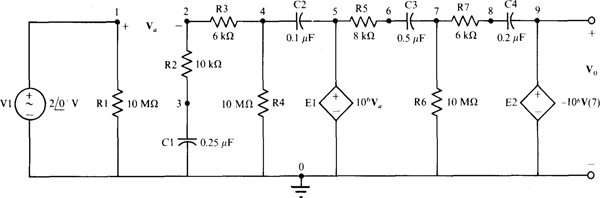
Fig. 13-34
Following is the circuit file for the circuit of Fig. 13-34 and also the results from the output file obtained when the circuit file is run with PSpice. The output of 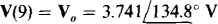 agrees with the answer to Prob. 13.27.
13.29 A 30-Ω resistor and a 0.1-H inductor are in series with a voltage source that produces a voltage of 120 sin (377t + 10°) V. Find the components for the corresponding phasor-domain current-source transformation.
Ans. A current source of  in parallel with an impedance of
13.30 A  voltage source is in series with a 6-Ω resistor and the parallel combination of a 10-Ω resistor and an inductor with a reactance of 8 Ω Find the equivalent current-source circuit.
Ans. A  current source and a parallel
  impedance
13.31 A  voltage source is in series with the parallel arrangement of an inductor that has a reactance of 100 Ω and a capacitor that has a reactance of —100 Ω. Find the current-source equivalent circuit.
Ans. An open circuit
13.32 Find the voltage-source circuit equivalent of the parallel arrangement of a  current source, a 60-Ω resistor, and an inductor with an 80-Ω reactance.
Ans. A  voltage source in series with a
  impedance
13.33 A  current source is in parallel with the series arrangement of an inductor that has a reactance of 100 Ω and a capacitor that has a reactance of — 100 Ω Find the equivalent voltage-source circuit.
Ans. A short circuit
13.34 In the circuit shown in Fig. 13-35, find the currents I1 and I2. Then do a source transformation on the current source and parallel  impedance and find the currents in the impedances. Compare.
Ans. 
 After the transformation both are
  So, the current does not remain the same in the
  impedance involved in the source transformation.
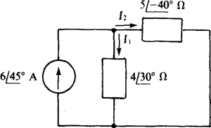
Fig. 13-35
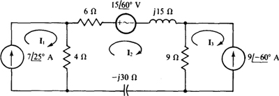
Fig. 13-36
13.35 Find the mesh currents in the circuit shown in Fig. 13-36.
Ans 
13.36 Find I in the circuit shown in Fig. 13-37.
Ans. 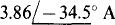
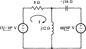
Fig. 13-37
Fig. 13-38
13.37 Find the mesh currents in the circuit shown in Fig. 13-38.
Ans. 
13.38 Find the mesh currents in the circuit shown in Fig. 13-39.
Ans. 

Fig. 13-39
13.39 Use loop analysis to solve for the current that flows down in the 10-Í2 resistor in the circuit shown in Fig. 13-39.
Ans. 
13.40 Use mesh analysis to find the current I in the circuit shown in Fig. 13-40.
Ans. 
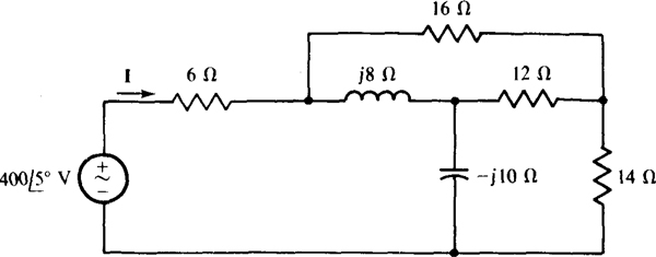
Fig. 13-40
13.41 Use loop analysis to find the current flowing down through the capacitor in the circuit shown in Fig. 13-40.
Ans. 
13.42 Find the current I in the circuit shown in Fig. 13-41.
Ans. 
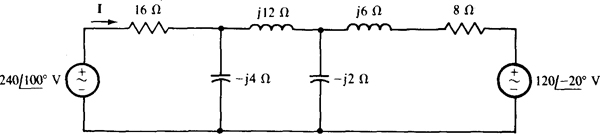
Fig. 13-41
13.43 For the circuit shown in Fig. 13-41, use loop analysis to find the current flowing down through the capacitor that has the reactance of — j2 Ω.
Ans. 
13.44 Use loop analysis to find l in the circuit shown in Fig. 13-42.
Ans. 
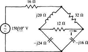
Fig. 13-42
13.45 Rework Prob. 13.44 with all impedances doubled.
Ans. 
13.46 Find the node voltages in the circuit shown in Fig. 13-43.
Ans. 
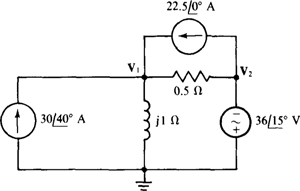
Fig. 13-43
13.47 Find the node voltages in the circuit shown in Fig. 13-44.
Ans. 
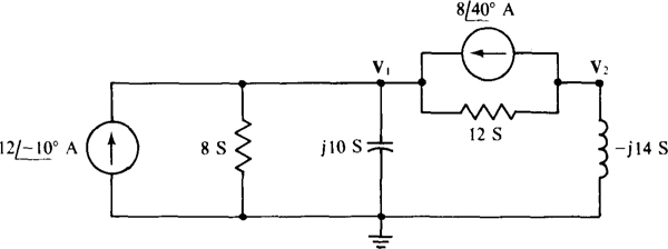
Fig. 13-44
13.48 Solve for the node voltages in the circuit shown in Fig. 13-45.
Ans. 
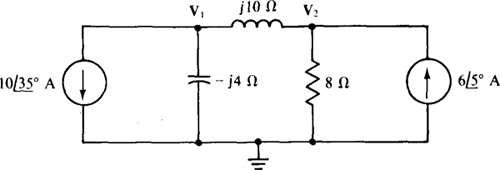
Fig. 13-45
13.49 Find the node voltages in the circuit shown in Fig. 13-46.
Ans. 
13.50 Solve for the node voltages of the circuit shown in Fig. 13-47.
Ans. 
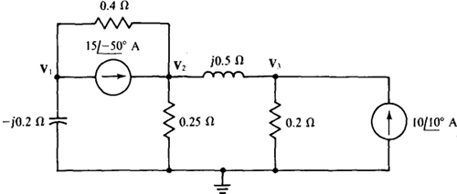
Fig. 13-47
13.51 For the circuit shown in Fig. 13-48, find V as a function of 1, and then find V as a numerical value.
Ans. 
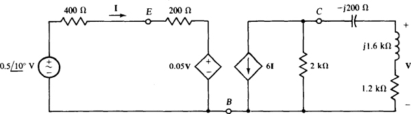
Fig. 13-48
13.52 Solve for I in the circuit shown in Fig. 13-49.
Ans. 
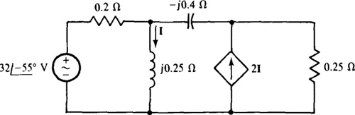
Fig. 13-49
13.53
Ans 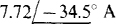
13.54
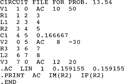
Ans 
13.55
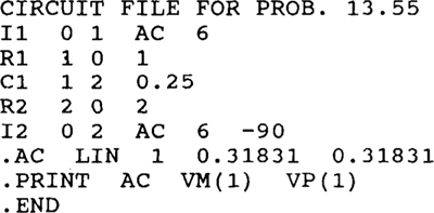
Ans 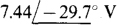
13.56
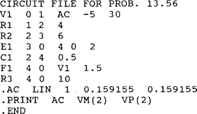
Ans 
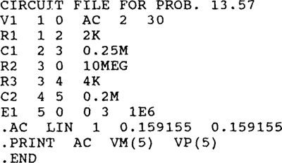
Ans 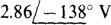
13.58
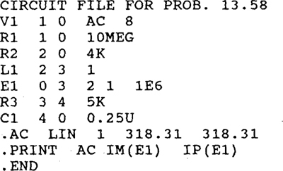
Ans 
 component voltage is the same as for the original circuit, but that the
  component voltage is different. This result illustrates the fact that a transformed source produces the same voltages and currents outside the source, but usually not inside it.