4.1 Fundamentals
4.1.1 PD Occurrence
localized electrical discharges that only partially bridge the insulation between conductors and which can or cannot occur adjacent to a conductor. Partial discharges are in general a consequence of local electrical stress concentrations in the insulation or on the surface of the insulation. Generally such discharges appear as pulses having durations of much less than 1 μs.
The first experimental study of PD signatures dates back to the year 1777 when Lichtenberg discovered dust figures like stars and circles. These appeared on the surface of an amber cake after it has been hidden by spark discharges up to 40 cm in length (Lichtenberg 1777, 1778). In the middle of the nineteenth century, besides the dust-figure technique initially used by Lichtenberg also photographs became a valuable tool to study PD phenomena, such as surface and interfacial discharges (Blake 1870; Toepler 1898; Müller 1927). At the beginning of the last century, when high alternating voltage was increasingly employed for long-distance power transmission links, it became known that partial discharges can be considered as a precursor for an ultimate breakdown, particularly when occurring in gaseous inclusions embedded in solid dielectrics. Since that time various tools, such as optical, chemical, acoustical and electrical methods, were increasingly used to detect partial discharges. Since the 1960s, the electrical PD measurement has become a widely established procedure for quality assurance tests of HV apparatus and their components, as will be discussed in more detail in the following sections.
Basically, partial discharges are caused by the ionization of gas molecules. Thus PD events occur not only in ambient air but also in gaseous inclusions in solid dielectrics or in gas bubbles and even in water vapour in liquid dielectrics. Therefore it is widely accepted that the discharge processes occurring in gaseous inclusions are comparable with those appearing in ambient air, such as Townsend and streamer discharges as well as leader discharges, which have extensively been investigated since the late 19th and early 20th centuries and published in numerous technical papers and text-books (Paschen 1889, Townsend 1915, 1925; Schumann 1923; Meek and Craggs 1953; Loeb 1956; Raether 1964; Park and Cones 1963; Devins 1984).

Photographs of discharge channels. a Streamer discharge in air (Lemke 1967). b Leader discharge in oil (Hauschild 1970). c Electrical trees in PMMA (Pilling 1976)

Time parameters of PD current pulses. a Theoretical pulse shape calculated by Bailey for small voids embedded in solid dielectrics. b Pulse shapes measured by Boggs and Stone for a sharp point (left) and a floating particle in SF6 (right)

Influence of the measuring frequency on the attenuation of a PD pulse travelling along a XLPE power cable of 16 m in length. a Experimental set-up. b Oscilloscopic record gained at overall bandwidth of 200 MHz. c Oscilloscopic record gained at overall bandwidth of 20 MHz
4.1.2 PD Quantities
As mentioned above, to evaluate the PD severity of HV apparatus in service, chemical, optical, acoustical and electrical PD detection methods are commonly employed. In the following, however, only PD quantities gained in the course of electrical PD measurements will be considered, as defined in IEC 60270:2000 as well as in the Amendment to this standard published in 2015.
- 1.
Apparent charge
Moreover it is noted in this standard, thatthat charge which, if injected within a very short time between the terminals of the test object in a specified test circuit, would give the same reading on the measuring instrument as the PD current itself. The apparent charge is usually expressed in picocoulombs (pC).
For more information in this respect see the Sects. 4.3 and 4.4, respectively.the apparent charge is not equal to the amount of charge locally involved at the site of the discharge, which cannot be measured directly.
- 2.
PD inception and extinction voltage

PC screenshots gained in the course of development tests of turbo-generators, rated voltage 24 kV. (a) Profile of the applied 50 Hz Ac test voltage (b) PD level of a “healthy” stator-bar under raising (red trace) and decreasing (green trace) test voltage (c) PD level of a “faulty” stator-bar

Impact of the background noise level on the determination of the inception and extinction voltage (explanation in the text)
- 3.
Phase-angle


Apparent charge pulses (pink traces) of Trichel discharges occurring in a 3.5 mm needle-plane gap under AC test voltage (green trace) displayed at a time base of 4 ms/div (a) and 0.4 ms/div (b), respectively

Oscilloscopic screenshots of apparent charge pulses (pink traces) gained for surface discharges (a) and cavity discharges (b) under power frequency test voltage (green traces)
- 4.
Pulse repetition rate


Oscilloscopic screenshot showing the PD signatures of a defective 110 kV transformer bushing at inception voltage Virms = 19 kV (a) and at highest phase-to-earth voltage being Vrms = 71 kV (b)
Note Based on further experimental studies it has been found that the extremely high magnitudes of the charge pulses displayed in Fig. 4.8 are the result of spark discharges originating in a transformer bushing on account of a poor grounding of the bushing tap terminal.
- 5.
Accumulated apparent charge


Oscilloscopic screenshot gained for a defective XLPE cable termination (rated voltage 24 kV) showing besides the apparent charge pulses (pink trace) also the accumulated apparent charge (green trace), where the recording time covers both half-cycles of the applied power frequency (50 Hz) test voltage (blue trace)
- 6.
Average discharge current


- 7.
Discharge power

- 8.
Quadratic rate

4.2 PD Models

Typical sizes of gaseous inclusions in solid dielectrics according to Kreuger (1989) a Flat cavity perpendicular to the electric field, b Spherical cavity, c Flat cavity aligned with the electric field, d Interfacial cavity
4.2.1 Network-Based PD Model

Experimental set-up used by Gemant and Philippoff (1932) to measure the breakdown sequence of the spark gap depending on the applied AC test voltage level

Oscilloscopic records taken by Gemant and Philippoff (1932) (a) and comparison with theoretical estimations (b)

Network-based PD model. a Plane-parallel electrodes with capacitive circuit elements. b Capacitive equivalent circuit (abc-model)
 is commonly considered, as illustrated in Fig. 4.13a. To simplify the following treatment the radius of the “healthy” dielectric column is assumed as equal to that of the gas-filled cylindrical cavity. Under this condition the equivalent capacitances Cb and Cc can simply be expressed by


 of the used solid dielectrics is commonly below 5. Under this condition follows from Eq. (10):
Due to this relation, the external charge detectable in the connection leads of the test object is referred to as apparent charge and it is noted in IEC 60270:2000 that the apparent charge is not equal to the amount of that charge involved at the site of the discharge, which cannot be measured directly.
4.2.2 Dipole-Based PD Model

Dipole model according to Pedersen (1986, 1987). a Space charge field due to bipolar point charges deposited at the cavity wall. b Circuit elements
To estimate the transient PD current through the equivalent capacitance Ca and thus through the test object shown in Fig. 4.14, the classical continuity equation applies. That means the conductive current  through the gaseous inclusion, represented in Fig. 4.14b by the capacitance Cc, equals the displacement current
  through the solid dielectric column represented by the capacitances
  and
and  , and continues thus also through the test object capacitance Ca, which causes a voltage jump ∆Va. That means, the external PD charge
 detectable at the terminals of the test sample equals the internal PD charge
 , which is given by the time-integral of the transient current flowing through the gaseous inclusion on account of the motion of the bipolar charge carriers. Obviously, this is in contrast to the classical
apparent charge
concept deduced from the previously considered network-based PD model.
, which is given by the time-integral of the transient current flowing through the gaseous inclusion on account of the motion of the bipolar charge carriers. Obviously, this is in contrast to the classical
apparent charge
concept deduced from the previously considered network-based PD model.
To estimate the PD charge transfer quantitatively, Pedersen proposed a field theoretical approach, which is based on the Maxwell equations (Pedersen 1986). However, this alternative concept has been ignored in the past, while the traditional abc-model is promoted also nowadays (Achillides et al. 2008, 2013, 2017). The reason for that is, apparently, that a PD charge transfer cannot easily be explained when Pedersens concept is adopted, because this needs an excellent knowledge of the field theory based on the Maxwell equations (Maxwell 1873). However, the analysis of the PD charge transfer can substantially be simplified when instead of spherical, ellipsoidal or cylindrical cavities, as frequently investigated and published in numerous technical papers, the establishment of a dipole moment under quasi-uniform field conditions is considered, i.e. the Laplacian field between the electrodes is assumed as constant for the time span required for the separation of the charge carriers (Lemke 2012, 2016). Therefore, to estimate the PD charge transfer, only the change of the Poissian field caused by the separation of the charge carriers of opposite polarity has to be analyzed.

Parameters used for the estimation of the field energy transferred to an electron and the associated positive ion


 neutral gas molecules can simply be expressed by
 , see Fig. 4.14b. For simplification it shall be assumed that at instant
  all charge carrier approached the dielectric boundaries. Under this condition the classical energy balance theorem can be written as follows:
 —the dipole moment created by the bipolar charge carriers, and Ei—the inception field strength. Separating the charge
  delivered from the test object capacitance Ca one gets
In this context it seems worth to notice that a similar approach can also be deduced using the concept of image charges (Shockley 1938; Kapcov 1955; Frommhold 1956). This has often been employed by many researchers to account for the displacement current associated with the motion of charge carriers between plane-parallel electrodes (Meek and Craggs 1953; Raether 1964).
 represents a reasonable quantity to assess the
PD severity
. So the density of the dielectric flux lines entering the electrodes and thus the danger for an ultimate breakdown increases at increasing cavity length dc, see Fig. 4.16. This is not reflected by the previously discussed network-based PD model, where the internal charge decreases at increasing cavity length, because this leads to a decrease of the cavity capacitance Cc.
represents a reasonable quantity to assess the
PD severity
. So the density of the dielectric flux lines entering the electrodes and thus the danger for an ultimate breakdown increases at increasing cavity length dc, see Fig. 4.16. This is not reflected by the previously discussed network-based PD model, where the internal charge decreases at increasing cavity length, because this leads to a decrease of the cavity capacitance Cc.
Distribution of the dielectric flux density depending on the distance dc between the positive and negative space charge
Note: With reference to the previously considered network-based PD model according to Fig. 4.14 it is noteworthy that the internal PD charge qc could be measured under the condition when all negative and positive charge carriers would be able to cross the entire distance between the anode and cathode. As can readily be shown under this condition the internal charge qc becomes equal to the measurable external PD charge qa. Based on the Eqs. (4.10b) and (4.17) it can thus be written:That means the “fictive” internal PD charge qc deduced from the network-based PD model equals that charge amount, which is carried by either the positive ions alone or even by the negative electrons alone. However, this is in contrast to the physics of gas discharges due to the fact that in case of a cavity discharge the charge amount carried by the positive ions is equal but of opposite polarity to that charge amount carried by the electrons and negative ions. Due to the very short distance between the bipolar space charges deposited at anode-side and cathode-side dielectric boundary, a great amount of the the positive space charge is compensated by the negative space charge, as can also be deduced from Fig. 4.16a. Consequently, the net charge attains only a low fraction of the unipolar charge carried by the positive ions alone, which is given by e ∙ ni, with ni—the number of ionized gas molecules.

 in field direction is substantially lower than the electrode spacing (Lemke 2013). As an example, consider Fig. 4.17, which refers to a spherical cavity embedded in the bulk dielectric between coaxial cylinder electrodes, as representative for power cables.
Parameters used for analyzing the PD charge transfer in extruded power cables

![$$ q_{a} \approx P_{m} \cdot \frac{1.2}{{r_{c} \left[ {\ln \left( {\frac{{r_{a} }}{{r_{i} }}} \right)} \right]}}. $$](../images/214133_2_En_4_Chapter/214133_2_En_4_Chapter_TeX_Equ21.png)
 quantitatively, however, is a challenge due to the fact that the number
  of ionized molecules is randomly distributed over an extremely wide range. Thus it seems reasonable to investigate only the worst case, which arises when streamer-like discharges are ignited. For this specific case the dipole moment can be expressed by the following semi-empirical approach (Lemke 2013):

 versus
  following from this approach is plotted in Fig. 4.18. For comparison purposes, experimental data are also plotted in this figure. In this context it should be noted that some experimental data refer to configurations other than the coaxial cylinder electrodes, as has been investigated here. Nevertheless, the calculated curve meets the measured data quite well, where a better agreement cannot be expected due to the inherent large scattering of the PD pulse magnitudes.
PD pulse charge qa versus cavity diameter dc calculated for a 20 kV XLPE cable and experimental data
 versus the
PD inception voltage V
i
is the most interesting function. To solve Eq. 4.17, the ratio
versus the
PD inception voltage V
i
is the most interesting function. To solve Eq. 4.17, the ratio  must be known. An appropriate approach to determine the inception voltage Ei versus the cavity diameter dc can be deduced from the Schumann curves (Schumann 1923), which reads:
 —the static inception field strength of ambient air under atmospheric reference conditions and
  a reference cavity diameter. Inserting these values in Eq. (4.17), one gets the following approach to determine the inception voltage of a virgin spherical cavity embedded in the bulk dielectric between coaxial cylinder electrodes:
![$$ V_{i} = \frac{{E_{0} }}{{k_{\varepsilon } }} \cdot r_{c} \cdot \left[ {\ln \left( {\frac{{r_{a} }}{{r_{i} }}} \right)} \right] \cdot \left( {1 + \sqrt {\frac{{d_{\text{r}} }}{{d_{c} }}} } \right) \approx V_{i} \approx \left( {10.5\;{\text{kV}}} \right) \cdot \left( {1 + \sqrt {\frac{{0.82\;{\text{mm}}}}{{d_{c} }}} } \right). $$](../images/214133_2_En_4_Chapter/214133_2_En_4_Chapter_TeX_Equ25.png)
 versus the inception voltage
  has been calculated for and plotted in Fig. 4.19. In this context it seems worth to notice that in IEC 60502:1997 a maximum test voltage level of 1.73 V0 is recommended for medium voltage cables with extruded insulation, where V0 represents the rms value of the phase-to-earth voltage. For the here considered 20 kV cable this is equivalent to a peak voltage of 28 kV. In Fig. 4.19a this value is indicated by a circle, which yields that the cable would pass the PD test only when the
PD level
remains below 5 pC. This result is in satisfying agreement with the recommendations of IEC 60502:1997, which specifies that the magnitude of the discharge at 1.73 V0 shall not exceed 10 pC. Moreover, it can be deduced from Eq. (4.23) that a PD inception voltage above 28 kV can only be guaranteed for a cavity diameter dc < 0.3 mm.
has been calculated for and plotted in Fig. 4.19. In this context it seems worth to notice that in IEC 60502:1997 a maximum test voltage level of 1.73 V0 is recommended for medium voltage cables with extruded insulation, where V0 represents the rms value of the phase-to-earth voltage. For the here considered 20 kV cable this is equivalent to a peak voltage of 28 kV. In Fig. 4.19a this value is indicated by a circle, which yields that the cable would pass the PD test only when the
PD level
remains below 5 pC. This result is in satisfying agreement with the recommendations of IEC 60502:1997, which specifies that the magnitude of the discharge at 1.73 V0 shall not exceed 10 pC. Moreover, it can be deduced from Eq. (4.23) that a PD inception voltage above 28 kV can only be guaranteed for a cavity diameter dc < 0.3 mm.
PD inception voltage versus PD charge (a) and cavity diameter (b) calculated for an XLPE medium voltage cable
Even if the calculated curves plotted in the Figs. 4.18 and 4.19 are in satisfying agreement with practical experience, it must be emphasized here that the quantitative values are only approximations. This is because Eq. (4.17) refers to a virgin cavity filled with ambient air under atmospheric normal conditions. However, for technical insulation, neither the cavity size nor the gas pressure are known. Moreover, the dipole moment established by subsequent PD events may strongly be affected by space charges deposited at the cavity walls on account of preceding PD events. This might also be the reason for the large scattering of the pulse charge magnitudes, as commonly encountered in practice.
4.3 PD Pulse Charge Measurement
4.3.1 Decoupling of PD Signals

Principle of pulse charge measurement
 flowing through the PD defect is provided only by the test object capacitance
  , which is associated with a fast voltage collapse
  across the test object. Following the dipole-based PD model, the
pulse charge
across the test object. Following the dipole-based PD model, the
pulse charge
 flowing through the PD defect is equal to that charge amount flowing through the capacitance Ca of the test object. Therefore it can be written:
At instant when the PD process is quenched and the charge carriers are deposited at the cavity walls, the PD current decays to zero so that the frequency content and thus the effective impedance of the HV connection leads decreases accordingly. Therefore the test object capacitance  will be recharged again by the HV test supply, i.e. the former voltage step
  appearing across Ca is compensated, which appears at inverted polarity. That means the time integral of the current recharging Ca and thus the apparent charge can also be assessed using Eq. (4.24), even if the actual shape of the recharging current is very different from that of the original PD current. This offers the opportunity to measure the PD pulse charge by means of a
measuring impedance
, if connecting the low voltage electrode of the test object to earth potential (Fig. 4.20). Additionally the terminals of the test object should be shunted by a HV capacitance
appearing across Ca is compensated, which appears at inverted polarity. That means the time integral of the current recharging Ca and thus the apparent charge can also be assessed using Eq. (4.24), even if the actual shape of the recharging current is very different from that of the original PD current. This offers the opportunity to measure the PD pulse charge by means of a
measuring impedance
, if connecting the low voltage electrode of the test object to earth potential (Fig. 4.20). Additionally the terminals of the test object should be shunted by a HV capacitance  to ensure that the entire current recharging Ca is flowing through the
measuring impedance
.
to ensure that the entire current recharging Ca is flowing through the
measuring impedance
.
 . Under this condition, the magnitude of the voltage jump appearing across
  is direct proportional to the pulse charge to be measured. At alternating test voltages, however, the capacitive load current flowing through the test object and thus through the
measuring impedance
could substantially exceed the signal level caused by the PD events, as exemplarily shown in Fig. 4.21a. To overcome this crucial problem, the measuring capacitance
is direct proportional to the pulse charge to be measured. At alternating test voltages, however, the capacitive load current flowing through the test object and thus through the
measuring impedance
could substantially exceed the signal level caused by the PD events, as exemplarily shown in Fig. 4.21a. To overcome this crucial problem, the measuring capacitance  is commonly shunted by a measuring resistor
  , which reduces the superimposed AC current accordingly, see Fig. 4.21b and c. Practical experience revealed, however, that a measuring impedance equipped with an RC network shown in Fig. 4.20 is only applicable for low-capacitive test samples used for fundamental PD studies, such as point-to-plane gaps, but not for PD tests of HV equipment and their components.
Records of typical voltage signals caused by PD events (pink trace), which were captured from an RC measuring impedance connected in series with a point-to-plane gap subject to AC test voltage (green trace)
 , as illustrated in Fig. 4.22. Here, the measuring resistor
  is shunted by an inductance Ls, which carries the entire alternating load current trough the coupling capacitor. The over-voltage protection unit
  is required to suppress fast over-voltages due to unexpected breakdowns and prevents thus a damage of the measuring impedance and the measuring instrument, as well. As the PD coupling unit shown in Fig. 4.22 provides a high-pass filter, it has to be taken care that the lower limit frequency
  is chosen as low as possible, preferably below 100 kHz.
PD measuring circuit, where the measuring impedance is connected in series with the coupling capacitor
Example To design a coupling device according to Fig. 4.22, which is intended for induced voltage tests of power transformers, the following parameters shall be assumed:
As the lower limit frequency is given bythe minimum capacitance of the coupling capacitor can be determined as follows:Inserting the maximum exciting frequency being fac = 400 Hz, one gets the following capacitive current through the coupling capacitor:As this current flows through the measuring resistor, a voltage drop as high as 1600 V would appear. Of course, this is dangerous for the operator and could also damage the connected PD measuring system. Thus, to reduce this high voltage drop, Rm should be shunted by an inductance Ls (Fig. 4.22). However, applying this option it has to be taken care that the lower limit frequency may significantly exceed the previously mentioned lower limit frequency, which should be chosen below 100 kHz. This condition is accomplished for
For the here considered maximum frequency fac = 400 Hz of the applied test voltage the inductive impedance attainsUnder this condition, the above mentioned load current of
flowing through the coupling capacitor of
causes a comparative low voltage drop across
, which attains 64 V. This value can further be reduced using a high-pass filter of higher order.
To display the PD pulse in a phase-resolved matter by means of an oscilloscope or even a computer-based PD measuring system, the PD coupling unit could further be configured using an additional measuring capacitor Cm, as illustrated in Fig. 4.22. Due to the very different frequency spectra of the PD pulses and the AC test voltage, these both signals can simply be discriminated. Considering Fig. 4.22, these appear at the outputs “PD pulses” and “test voltage”. If, for instance, the above-introduced maximum test voltage level of Vac = 200 kV should be attenuated down to 50 V, a divider ratio of 1:4000 would be required. Using a coupling capacitor of Ck = 3.2 nF, a low-voltage measuring capacitance of Cm = 12.8 μF would be required.


4.3.2 PD Measuring Circuits According to IEC 60270

Basic PD measuring circuits recommended in IEC 60270:2000. a Measuring impedance in series with a coupling capacitor used for grounded test objects. b Test object grounded via the measuring impedance. c Bridge circuit recommended for noise reduction

Photograph of a PD measuring circuit designed according to IEC 60270.
Courtesy of Doble Lemke
Electromagnetic noises interfering sensitive PD measurements can also be eliminated to a certain extend using the so-called balanced PD bridge according to Fig. 4.23c. Here, the adjustable measuring impedances Zm1 and Zm2 are installed in the ground connection leads of both the test object and the coupling capacitor providing the measuring branch and the reference branch, respectively. Adjusting  and
and  accordingly to balance the bridge, common mode noises appearing at the high-voltage terminals are more or less suppressed by the differential amplifier. Thus only the PD signal originating in the test object appears at the output of the differential amplifier and is thus measured by the PD instrument. To ensure a high common mode rejection, the bridge should be designed as symmetrical as possible. Thus it is advisable to use instead of the coupling capacitor a complementary PD-free test object as a reference. Despite of the benefits of the balanced bridge for noise suppression, this approach is not generally employed in practice because the design is a challenge due to the fact that both branches must have an equivalent frequency response over the full bandwidth used for the PD signal processing. Moreover it has to be taken into account that the time-delay of the interfering signal traveling along the complementary PD-free test object is equal to that signal traveling along the test object under investigation.
 measurements. Here the HV bushing capacitance C1 provides in principle the coupling capacitor
  shown in Fig. 4.23a.
Bushing tap coupling mode commonly used for PD tests of power transformers
4.3.3 PD Signal Processing

Frequency spectrum of PD pulses in comparison to the frequency band recommended for PD pulse charge measurements according to IEC 60270:2000

Note According to IEC 60270: 2000, the term “wide-band” refers to the band-pass filter characteristics of the PD processing unit characterized by a bandwidth ∆f = f2 − f1, which is substantially greater than the lower limit frequency f1. In this context, it must be emphasized that this term is not correlated with the frequency spectrum of real PD current pulses, which covers often a frequency range up to the GHz range, see Sect. 4.1.
 and
and  respectively, is shown in Fig. 4.27a. Based on the network theory it can be stated that the peak value of the output pulse is proportional to the time integral of the input pulse where the duration of the output pulse is substantially greater than that of the input pulse.
PD pulse responses of a wide-band (a) and a narrow-band (b) processing unit. a Lower limit frequency  and upper limit frequency
  . b Mid-band frequency
  and bandwidth ∆f = 9 kHz
In this context it should be noted that the integration performance is only governed by the
upper limit frequency
f2 and not by the lower limit frequency f1. Thus also narrow-band filters could in principle be used to accomplish a quasi-integration. For this purpose the bandwidth  must be chosen substantially lower than the center frequency
  . As a typical measuring example, consider Fig. 4.27b, which refers to the PD pulse response of a narrow-band amplifier characterized by a center frequency of
  and a bandwidth of
  . Here the maximum peak-to-peak value of the oscillating response is direct proportional to the pulse charge injected in the the narrow-band amplifier, which follows also from the classical network theory (Schon 1986). In IEC 60270:2000 the following frequency parameters are recommended for narrow-band PD instruments:


 accordingly, see Sect. 4.5. In this context it must be emphasized, however, that fatal superposition errors may appear due to the comparatively long duration of the oscillating response, which exceeds often several hundreds of μs. As an example consider Fig. 4.28, which refers to the double-pulse response of a narrow-band amplifier. Here the time interval between two subsequent appearing impulses was reduced from originally 1.4 µs down to 0.7 µs. As can be seen, the peak-to-peak values of the oscillating signal decreases substantially under this condition. Such a behavior is typical for PD pulses decoupled from power cables due to their reflection at the cable ends. Moreover, superposition errors may also occur on account of oscillations excited by PD events in the windings of rotating machines and power transformers. This is the reason why narrow-band amplifiers are in general not recommended for measuring the apparent charge of PD pulses in terms of pC.
Impact of the double-pulse distance on the oscillation magnitude of a narrow-band PD processing unit
4.3.4 PD Measuring Instruments
4.3.4.1 General
Schering bridges in combination with oscilloscopes can be considered as the first instruments used for the electrical PD detection. However, the measuring sensitivity was comparatively low. This was substantially increased in the 1920s when the first super-heterodyne receivers equipped with narrow-band amplifiers were available (Armann and Starr 1936; Dennhardt 1935; Koske 1938; Lloyd and Starr 1928; Müller 1934; Schering 1919). To ensure comparable and reproducible PD measurements, the requirements for such instruments were first specified in the USA and North America in 1940, when the standard “Methods for Measuring Radio Noise” was published by the “National Electrical Manufactures Association NEMA”. This standard was later revised by the NEMA Publication 107 “Methods of Measurement of Radio Influence Voltage (RIV) of High-Voltage Apparatus” and issued in 1964. An equivalent standard for RIV measurements of HV apparatus was also edited in Europe by the “Comité International Spécial des Perturbation Radioélectrique (CISPR)”, published in 1961.
Radio interference voltages (RIV) are commonly measured in terms of µV and weighted according to the acoustical noise impression of the human ear. Therefore it cannot be expected that these are correlated to the apparent charge of PD pulses measured in terms of pC, as can readily be proven experimentally (Harrold and Dakin 1973; Vaillancourt et al. 1981). Moreover, fatal superposition errors might appear at high PD pulse repetition rate or even in case of reflections and oscillations excited by the fast PD transients in cables and inductive components, as has been discussed previously. As a consequence, the “International Technical Commission (IEC), Technical Committee No. 42: High-Voltage Testing and Measuring Technique” decided the edition of a separate standard on PD measurements. The first edition of “IEC Publication 270” appeared in 1968, where besides the definition of the PD quantity “ apparent charge ” as well as the inception and extinction voltage, several other PD quantities were introduced, such as the repetition rate as well as the power of consecutive PD pulses. Additionally, rules for calibrating PD measuring circuits were specified, and guidelines were attached which supported the identification of typical PD defects under AC test voltage based on oscilloscopic records using either the elliptical or the linear time base to record the characteristic PD pulse trains in a phase-resolved manner.
The second edition of IEC Publication 270, published in 1981, contained more details on the calibration procedure. Additionally, the PD quantity “largest repeatedly occurring PD charge” was specified. Based on this standard, the electrical PD measurement became an indispensable tool for tracing dielectric imperfections in HV apparatus, which might be caused by design failures as well as by a poor assembling work. Therefore, the measurement of partial discharges was increasingly requested with respect to increased quality requirements, which was also forced by the enhancement of the design field strength and, last but not least, by demands concerning the enlargement of the lifetime of HV equipment.
The following treatment is based on the third edition of IEC 60270 published in 2000, which can be considered as an extensive revision of the second edition. The specification covers besides the traditional analogue PD signal processing also the advanced digital acquisition of the captured PD pulses. Moreover, a section has been added, which refers to maintaining the characteristics of PD measuring systems and the associated calibrators, as will be considered more in detail in Sect. 4.3.7.
4.3.4.2 Analogue PD Instruments

Simplified block diagram of an analogue PD instrument
 and
and  respectively, to accomplish the pulse train response according to Fig. 4.31. In this context it should be emphasized that this approach ensures more or less reproducible test results under power frequency (50/60 Hz) AC voltages, but not when the test frequency is changed, as usual for quality assurance tests of power transformers and instrument transformers, where the test frequency is occasionally increased up to 400 Hz. This has also to be taken into account when resonance test sets are used for on-site PD tests of power cables, where the test frequency is often varied between 20 Hz and 300 Hz (Rethmeier et al. 2012).
Screenshots gained by means of a computerized PD measuring system showing the PD level of a MV power cable termination under AC (50 Hz) voltage (test level 38 kV, recording time 120 s). a Peak values of each individual charge pulse. b Largest repeatedly occurring PD magnitude weighted according to IEC 60270:2000

Pulse train response specified in IEC 60270:2000 to measure the largest repeatedly occurring PD magnitude
To evaluate PD test results, it is highly recommended to display the phase-resolved PD patterns (PRPDP), which supports the identification of potential PD defects and enables often the discrimination of disturbing noises from real PD events. For this purpose, either the built-in oscilloscope or even an external connected multichannel oscilloscope as well as a computerized measuring system can be used.
As discussed previously, narrow-band instruments are commonly not capable of measuring the apparent charge of PD pulses in terms of pC. Nevertheless, such devices, which are commonly designed to measure radio interference voltages (RIV) as well as to investigate the electromagnetic capability (EMC) of electronic devices, are nowadays also widely employed for PD measurements, particularly for PD diagnosis tests of HV apparatus under on-site condition due to their excellent noise immunity. Even if such instruments measure the captured PD signal in terms of μV and not in terms of pC, there is no doubt that the PD inception and extinction voltage as well as the change and the trend of the PD activity can well be determined by means of narrow-band instruments.
4.3.4.3 Digital PD Instruments
Due to the recent achievements in micro-electronics and in particular in digital signal processing (DSP), the traditional analogue PD instruments are nowadays increasingly replaced by advanced digital PD measuring systems. The first concept of a computerized PD measuring instrument has been presented by Tanaka and Okamoto (1978). After that time, various solutions for computer-based PD measuring systems have been proposed, for instance, by Kranz (1982), Haller and Gulski (1984), Okamoto and Tanaka (1986), van Brunt (1991), Gulski (1991), Kranz and Krump (1992), Fruth and Gross (1994), Shim (2000), Lemke et al. (2002), Plath et al. (2002).

Block diagram of digital PD instruments. a Analogue pre-processing of the PD signal followed by an A/D conversion of the apparent charge pulses. b Direct A/D conversion of the wide-band amplified PD pulses
-

instant of PD occurrence
-

pulse charge at instant

-

test voltage value at instant

-

phase angle at instant

Statistical analysis based on phase-resolved 2D and 3D patterns and pulse sequence pattern to classify and identify PD sources as well as to cancel electromagnetic noises.
Clustering the PD pulses in homogenous families, based on waveform analysis and spectral amplitude diagrams in order to separate the characteristic patterns of PD events originating in different dielectric imperfections.
Localization of PD faults in power cables and GIS using time-domain reflectometry as well as in the windings of rotating machines and power transformers using multichannel techniques.

4.3.5 Calibration of PD Measuring Circuits
 required to measure the apparent charge
  of PD pulses, which is deduced from the reading
  of the PD measuring instrument or even from the signal magnitude displayed on the screen of an oscilloscope or a computer. For this purpose, a well known calibrating charge
  is injected between the terminals of the test object. Provided this causes the reading M0, the apparent charge can be calculated for using the following relation:
 across Ca detectable between the terminals of the test object, see Sect. 4.2. An equivalent response appears when a calibrating charge is injected between the terminals of the test object, as illustrated in Fig. 4.34 (Lemke et al. 1996; Lukas et al. 1997).
Principle of the calibration procedure used to determine the scale factor of PD measuring systems
Example Assuming a calibrating charge of q0 = 20 pC, which is injected between the terminals of the test object and causes a deflection of 5.4 divisions on the display of an oscilloscope, which is connected to the output of the PD instrument. Thus, the scale factor becomes Sf = 20 pC/ 5.4 div = 3.7 pC/ div. Performing an actual PD test, where a recorded PD pulse causes a maximum deflection of 8.6 div, the apparent charge amounts qa = (3.7 pC/ div) × 8.6 div ≈ 32 pC.
 and
and  shown in Fig. 4.34 are substituted by only a single calibrating capacitor
  , which is commonly connected between the internal pulse generator of the calibrator and the HV terminal of the test object in order to inject the calibrating charge, see Fig. 4.35.
PD Calibrator connected to a 20 kV instrument transformer

Set-up to demonstrate the step pulse response of a transformer bushing (a) and characteristic signals injected at the HV terminal (CH1) and decoupled from the bushing tap (CH2) as well as from the output “apparent charge” of the connected PD measuring instrument (CH3) (b)

Step voltage parameters specified for PD calibrators in the Amendment to IEC 60270:2000, published in 2015

To minimize distortions of the step voltage shape, which may occur at comparatively high capacitive load, the calibrating capacitor  should be chosen not greater than 200 pF. Additionally, the condition
  should be satisfied to accomplish the complete charge transfer to the test object capacitance Ca via the calibrating capacitance C0.
4.3.6 Performance Tests of PD Calibrators
 created by the calibrator into a measuring capacitor Cm, see Fig. 4.38a. To accomplish the entire charge transfer from the calibrator to Cm, which is required to apply the relation
  the condition
  must be satisfied. If, for instance, the calibrator is equipped with a capacitor of
  , the measuring capacitor should be chosen as high as
  . Applying a conventional foil capacitor to guarantee a high-temperature stability, however, the front of the step pulse may be distorted drastically on account of the inherent inductive component, as exemplarily shown in Fig. 4.38b. This record refers to a calibrating charge of
  , which was injected via a 100 pF series capacitor into a 20 nF measuring capacitor. To overcome this crucial problem, an appropriate damping resistor
  should be connected between calibrator and measuring capacitor, which leads to a response comparable to that shown in Fig. 4.38c. Another option to reduce the effective inductance is the use of numerous measuring capacitors connected in parallel.
Set-up for measuring the calibrating charge (a) and typical oscilloscopic records gained by the use of damping resistors by Rd = 50 Ω (b) and Rd = 390 Ω (c), respectively
 injected in a 10 nF measuring capacitor causes a voltage jump as low as
  i.e. a change in voltage as low as 0.2 mV must be recognized to achieve an appropriate measuring accuracy. To overcome this crucial problem, an electronic integrator could be employed to enhance the measuring sensitivity accordingly (Lemke 1996). A schematic diagram of such a circuit is shown in Fig. 4.39, which ensures the complete charge transfer from the calibrator to the capacitor
  even if the capacitance of Cm is reduced 100 times, i.e. from originally 10 nF down to about 100 pF, where the latter equals the value of the calibrating capacitor C0. As obvious from the oscilloscopic records shown in Fig. 4.39, which refers to a calibrating charge of approx. 3 pC, a sufficient high-voltage step of approx. 30 mV is achieved, which can conviently be measured at desired accuracy, in particular when the oscilloscope is equipped with an averaging tool. In this context it should also be noted that despite the comparatively low integrating capacitance of only 100 pF the decay time constant of the measured signal is sufficiently high (Fig. 4.39c), so that the recorded voltage signal CH2 decreases only marginally during the recording time, which is chosen as 5 μs and corresponds thus to the minimum duration
  of the step voltage response specified in the Amendment to IEC 60270:2000.
Principle of an electronic integrator for measuring the charge of PD calibrators (a) and typical signals recorded at time scale of 100 ns/div (b) and 1 μs (c), respectively
 , as illustrated in Fig. 4.40a. Obviously, the series connection of
  and
and  represents a high-pass filter, so that the time-dependent voltage
  appearing across
  must be integrated again to determine the charge
  created by the calibrator. For this purpose, a digital oscilloscope equipped with a feature for numerical integration could be be employed, where the A/D converter should have a vertical resolution not lower than 10 bits at 50 MS/s sampling rate to achieve an adequate resolution of the input signal. Additionally, the analogue bandwidth should be not lower than 50 MHz. Generally, digital oscilloscopes calibrated in compliance with IEC 61083-1:2002 should only be employed.
Set-up recommended for a numerical integration of the calibrating charge  injected in a measuring resistor of Rm = 50 Ω (a) and typical oscilloscopic records (b) gained for a calibrating charge of
4.3.7 Maintaining the Characteristics of PD Measuring Systems
- 1.
The routine calibration of the complete PD measuring system connected to the HV test circuit. This should be performed just prior a PD test, where the calibration provides the scale factor Sf of the entire measuring system to be used in the actual PD test. Nowadays, this procedure is mainly used to adjust the reading of the PD measuring instrument to obtain a direct reading of the PD magnitude, i.e. Sf should satisfy preferable values (e.g. 1, 2, 5, 10, 20…). For this routine calibration, there are no major changes as compared to the IEC 270 edited in 1981.
- 2.
The determination of the specified characteristics of the complete PD measuring system should be performed at least once a year or after major repair.
- 3.
The calibration of the PD calibrator itself, as presented above.
Nominal characteristics (identification; operation conditions, measuring range, supply voltage)
Type test results
Routine test results
Performance test results (date and time)
Performance check results (date and time; result: passed/failed: if failed: action taken)
- (a)Type tests are to be done by the manufacturer and shall be performed for one PD measuring system of a series and shall at least include the determination of the following parameters:
The frequency-dependent transfer impedance Z(f) as well as the lower and upper limit frequencies f1 and f2 over a frequency range in which it has dropped to 20 dB from the peak band-pass value;
The scale factor k to calibrating pulses of at least three different pulse charge magnitudes ranging between 10 and 100% of the full reading at a pulse repetition rate n around 100 s−1. In order to prove the linearity of the PD measuring instrument, the variation of k shall be less than 5%;
The pulse resolution time Tr by applying calibration pulses of constant magnitude but decreasing time interval between consecutive pulses;
The pulse train response for pulse repetition rates N ranging between 1 s−1 and >100 s−1.
- (b)
Routine tests are to be done by the manufacturer and shall include all tests required in a performance test as listed below. Routine tests shall be performed for each measuring system of a series. If the test results are not available from the manufacturer, the required tests shall be arranged by the user.
- (c)Performance tests shall include the determination of the following parameters:
The frequency-dependent transfer impedance Z(f) as well as the lower and upper limit frequencies f 1 and f 2 over a frequency range in which it has dropped down to 20 dB from the peak band-pass value.
The linearity of the scale factor k to be verified between 50% of the lowest and 200% of the highest specified PD magnitude. Using calibrating pulses of adjustable magnitude having a repetition rate of approximately n = 100 s−1, the scale factor k shall vary not more than 5%.
- (d)
Performance checks shall include the determination of the transfer impedance Z(f) at one frequency selected in the band-pass range in order to verify that the value deviates not more than 10% from that one recorded in the performance test.
- (a)
Type tests are to be done by the manufacturer and shall be performed for one PD calibrator of a series. Type tests shall include at least all tests required in a performance test. If results of type tests are not available from the manufacturer, the required tests for verification the technical parameters of PD calibrators shall be arranged by the user.
- (b)
Routine tests are to be done by the manufacturer and shall include all tests required in a performance test. Routine tests are to be performed by the manufacturer for each measuring system of a series. If the test results are not available from the manufacturer, the required tests shall be arranged by the user.
- (c)Performance tests shall include the determination of the following parameters:
The actual magnitude of the pulse charge q0 for all nominal settings, where a measuring uncertainty within 5% or 1 pC, whichever is greater, is acceptable.
Rise time tr of the voltage step U0, where a measuring uncertainty within 10% is acceptable.
Pulse repetition frequency N, where a measuring uncertainty within 1% is acceptable.
- (d)
Performance checks include the determination of the actual magnitude of the calibrating charge q0 for all nominal settings, where a measuring uncertainty within 5% or 1 pC, whichever is greater, is accepted.
4.3.8 PD Test Procedure

Set-up applied for a PD tests of a power transformer under induced voltage using the bushing tap coupling mode
- (a)
Configuration of the HV test circuit:

Shielding electrodes assembled at the top of the bushings of a 500 kV single-phase transformer intended to prevent disturbing corona discharges
- (b)
Adjustment of the measuring frequency range :
 should be selected preferably below 300 kHz, while the lower limit frequency
  should be adjusted below 100 kHz to ensure a PD signal processing in a wide-band range. Reducing
  substantially below 100 kHz, however, serious disturbances might appear due a possible iron core saturation as well as other core-related noises and even harmonics superimposed on the exciting AC voltage.
- (c)
PD calibration :
 injected into the top electrode of the bushing and the reading
  of the PD instrument, which provides the scale factor
  , as pointed out in Sect. 4.3.5. The ground connection lead between calibrator and transformer tank should be of low inductance and should thus be kept as short as possible. To prove the linearity of the PD measuring system, calibrating charges of different magnitudes should be injected. If, for instance, the full reading of the PD instrument is obtained for a calibrating charge of 200 pC, it is recommended to reduce thereafter the calibrating charge down to 100 pC and at least to 50 pC. Under this condition the deviation of the reading from that to be expected for a linear operating instrument should be below 10% of the full reading. After the calibration procedure has been finished it has to be taken care that the calibrator is removed from the test object to avoid any damage when the HV test voltage is switched on.
- (d)
Actual PD test under HVAC voltage:
 to determine the “energized background noise level” in terms of pC. This should not exceed the 50% value of the specified apparent charge, which is being accepted. Thereafter, the test voltage has to be raised up to the specified 1 h test value
  and held constant for few minutes to verify whether there are any PD problems. If not, the test voltage has then to be raised up to the enhancement (withstand) level
  and held constant for 7200 cycles in order to observe the PD trend.
Profile of the HVAC test voltage recommended in the IEEE Standard C57.113 for PD testing of liquid-filled power transformers and shunt reactors
Note As HVAC test voltages substantially higher than the rated voltage are applied, the exciting frequency must be enhanced accordingly, which can conveniently be realized by the use of HVAC test sets of variable test frequency. For this reason, the duration of the PD test period at enhancement voltage level is expressed in terms of cycles. If, for instance, a test frequency of 120 Hz is applied, 7,200 cycles are equivalent to a test period of 60 s. For more details in this respect see Sect. 3.2.5.
 . Under this condition, the apparent charge is recorded at subsequent five-minute intervals, where the recording time can be limited to about 1 min at each interval.
- (e)
Evaluation of PD test results:
is below a specified value in terms of pC,
is within a specified tolerance band,
does not exhibit any steadily rising trend, and
does not suddenly increase during the last 20 min of the 1 h test period.
In this context, it has to be taken into account that during the above mentioned 5-min test intervals sporadic noises may be encountered, for instance, by the switching of cranes. Provided, the test results do not comply with the specified limits, the PD-tested transformer should not warrant immediate rejection but lead to consultation between purchaser and manufacturer to decide further actions.
4.4 PD Fault Localization
To assess the PD severity, besides the apparent charge and the PD pulse repetition rate also the origin of the PD source should be known. This is particularly of importance for high-polymeric power cables, where the insulation may irreversibly be deteriorated by PD events having a magnitude of only few pC. Therefore, the localization of PD failures became a well established method since the 1970s, when high-polymeric power cables where increasingly used in distribution networks (Eager and Bahder 1967, 1969; Lemke 1975, 1979; Beinert 1977; Kadry et al. 1977; Beyer and Borsi 1977). The main benefit of the PD fault localization in power cables is on one hand, that the reason for typical PD defects can be clarified so that the technology for manufacturing such cables can be improved. On the other hand, the entire cable length must not be replaced in case of a single PD failure, but rather that short section containing the PD defect. In this context it should be noted that in case of routine tests most of the recognized PD failures appear at the cable ends, mainly due to a poor assembling of the stress cones required for a field grading.
 has to be determined. As a measuring example consider Fig. 4.44a. Here, a calibrating pulse was injected in that cable end where the coupling unit is connected, which is usually referred to as near cable end. As electrically long power cables behave like an electromagnetic waveguide, the pulse injected at the near end travels first at wave velocity
  towards the far or remote cable end, where the signal is reflected, and thereafter towards the near cable end. Consequently, a second pulse is also detectable at the near cable end after a time span tc required for travelling twice the entire cable length, i.e. 2 ∙
  . Hence the travelling wave velocity can simply be accounted for using the following relation
Principle of PD fault localization in electrically long power cables. a Determination of the travelling wave velocity. b Using the time-domain reflectometry (TDR) to determine the PD site

 between PD site and remote cable end and thereafter the distance xn, which is equal to that travelled by the direct PD pulse. Based on this it can be written:

Nowadays available computerized PD measuring systems are mostly equipped with features for time-domain reflectometry (TDR) to localize PD failures in power cables (Lemke et al. 1996, 2001). The main challenge is, however, to measure the time difference  between the direct and the reflected PD pulse as accurately as possible, which requires an A/D conversion at sampling rate not lower than 100 MS/s and a signal resolution of 10 bit. To record the complete PD data stream occurring during a single half-cycle of a 50-Hz test voltage, the memory depth should be in the GByte range. The overall bandwidth should cover a frequency range between about 50 kHz and 20 MHz.

Screenshots of a computer-based PD fault localization system (explanation in the text)
- (a)
Inserting the cable data: Besides the fundamental cable parameters (manufacturer, type and insulation of the cable, rated voltage, operation voltage, recently performed tests, etc.) this should include the test voltage parameters to be applied (test voltage levels, number of shots at each test voltage level), also the cable length and the positions of the accessories (joints and terminations), which are especially of interest to localize the PD defects as accurate as possible.
- (b)
Calibration : This includes the determination of both the measuring sensitivity and the travelling wave velocity of the PD pulses. As shown in Fig. 4.45a, besides the calibrating pulse injected at the near cable end, several pulse reflections might occur, where only the first one is of interest. Therefore, this signal is zoomed, as obvious from Fig. 4.45b, and the cursors are set accordingly by the computer software to determine the time interval
 and thus the travelling wave velocity
  based on Eq. 4.26 as precisely as possible.
 - (c)
PD measurement : Recording of the consecutive PD pulses occurring within a pre-selected time interval (Fig. 4.45c) and evaluation the of the PD pulse magnitudes. For this purpose each PD pulse magnitude is initially indicated in terms of Volts, and based on this the pulse charge appearing at each test voltage application is calculated for by the software and stored in the computer memory to perform a statistical analysis of the data stream.
- (d)
PD fault localization : To apply the time-domain reflectometry (TDR), only those PD pulses showing typical reflections within the time interval tr ≤ 2 tc are extracted. Thereafter, these pulses are zoomed and the cursors are set accordingly to measure the time interval between each direct and the associated reflected pulse, see Fig. 4.45d. Based on this, the distance between PD source and either the near or the remote cable end is determined. This procedure is repeated several times in order to perform an averaging and thus to enhance the measuring accuracy. Occasionally, a digital filtering of the captured signal may be performed to minimize the impact of radio interference voltages on the test results.
- (e)
PD mapping : Displaying all determined fault positions and the associated pulse charge magnitudes along the cable length. A typical measuring example for this is shown in Fig. 4.45e, which refers to a 20 kV XLPE cable of 480 m in length having two potential PD defects. The first one is located at 3 m from the near end and the second one at 452 m. Usually, the PD fault localization is performed automatically by the software. Only if a repair of an identified joint or termination is decided, the manual feature should additionally be applied to prove the validity of the automatically located PD sites. For more information in this respect see also the Sects. 7.1.3 and 10.2.2.2.
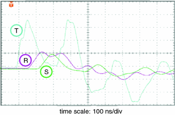
PD signals decoupled simultaneously from the three phases (R, S, T) of a power transformer using the bushing tap coupling mode

Characteristic PD signatures captured from the cable terminations connected to a three-phase gas-insulated switchgear
Another approach to distinguish between different PD sources is the presentation of typical clusters in a 3-phase amplitude relation diagram, which is based on a synchronous multichannel PD measurement (Emanuel et al. 2002). An enhancement of this method is the presentation of so-called three-center-frequency relation diagrams where three different frequencies selected from the complete spectrum of a single PD pulse are evaluated and displayed on the computer screen. This feature provides not only valuable information on the discharge nature itself but can also be used to localize the origin of PD defects (Rethmeier 2009). For more details in this respect see Sect. 4.6.
Another promising tool proposed for the localization of potential PD defects in HV equipment is the so-called pulse waveform analysis. This is based on the extraction of a set of PD pulse parameters, such as the rise time and the decay time as well as the PD pulse width (Montenari 2009). Displaying the characteristic clusters like star diagrams, multiple PD failures can also be recognized, as presented also in Sect. 4.6.
In this context, it should be noted that besides the above-described electrical methods, also the acoustic emission (AE) technique is widely used, in particular to localize PD defects in metal-encapsulated HV apparatus, such as gas-insulated switchgears (GIS) and gas-insulated lines (GIL) as well as large power transformers. The combination of both the electrical and acoustic method can also be very effective, for instance, to enhance the signal-to-noise ratio. For more information in this respect see Sect. 4.8.
Even if the localization of PD faults is nowadays performed by means of advanced computerized PD measuring systems, it should not be overlooked that commercially available digital oscilloscopes can also conveniently be employed for this purpose. In this context it should also be emphasized that a great deal of practical experience is required to decide if a HV equipment showing a high PD activity should really be taken out of order or even kept in service and PD monitored permanently to recognize a sudden increase of the PD activity and thus to prevent an unexpected breakdown. For more information in this respect see Sect. 10.3.
4.5 Noise Reduction
4.5.1 Sources and Signatures of Noises
The PD signal level to be detected is often in the mV range and below and may thus be disturbed by electromagnetic noises in the measuring surroundings. To discriminate such interferences from the PD signal, the sources and signatures of typical noises must be known. Depending on the mode of propagation it is generally distinguished between radiated noises and conducted noises .
Noises radiated from radio broadcast stations appear usually modulated and enter the test area via the electromagnetic field, where the HV electrodes and measuring loops of the PD test circuit act like antennas. Moreover, high-frequency transients associated with corona discharges igniting in the vicinity of the test area at sharp edges and protrusions on the surface of HV electrodes can also be classified as radiated noises.

Signatures of stochastically appearing pulse-shaped noises. a Maintenance work (drilling worker), b Car starting nearby, c Switching of a crane in the test lab

Signatures of periodically appearing pulse-shaped noises. a Protrusion at the surface of a HV shielding electrode. b Sharp edge of a metallic structure on ground potential. c Sparking between metallic parts on floating potential. d Frequency converter feeding a resonant test set of variable frequency. e Defective xenon lamp in the control room
4.5.2 Noise Reduction Tools
To minimize the impact of radiated noises it is a common practice to erect electromagnetically well-shielded test laboratories , as described in Sect. 9.2.2, where the fundamental laws of HF technology have to be taken into consideration. Particularly wire loops acting as inductive antennas should be kept as low as possible in cross-section to minimize the induction of interferring voltages on account of radiated noises. Moreover, the ground connection leads should also be of low inductance which is best accomplished by using Cu or Al foil.
If PD test laboratories are not carefully shielded against radiated electromagnetic noises, it could be helpful under certain conditions to use the balanced bridge circuit according to Fig. 4.23c. Practical experiences revealed that for comparatively small test objects, such as instrument transformers and bushings, the signal-to-noise ratio can be enhanced by a factor up to 10. However, for tall test objects, such as power transformers, this method is commonly not effective.
An option of the bridge method is the pulse polarity discrimination , originally proposed by Black (1975), where a balance procedure is not required. As the PD pulses decoupled from both bridge branches appear at opposite polarity, these can conveniently be discriminated from radiated electromagnetic noises because these appear unipolar. For tall test objects, however, this method is commonly not applicable because the PD pulses transmitted via both bridge branches might excite oscillations, so that the true polarity is lost.

Oscilloscopic screenshots gained for a 20-pC calibrating pulse injected in a XLPE cable: CH1: Input signal captured from a wide-band measuring impedance; CH2: Signal after conventional band-pass filtering; CH3: Signal after non-conventional wide-band amplification  followed by an electronic integration

Block diagram of a non-conventional wide-band PD measuring system equipped with various de-noising tools, as described in the text
Wide-band amplification of the PD signal captured from the measuring impedance, where a bandwidth up to about 20 MHz seems reasonable.
Automatic gating of pulse-shaped noises appearing periodically and even stochastically. To receive the noisy signals for triggering the gating unit, the rod or loop antennas should be installed as close as possible to the supposed noise sources.
Canceling of radio interference voltages. This is achieved by adjusting the threshold level for passing the RIV rejection unit slightly above the noise level, which is controlled automatically.
Electronic integration of the de-noised PD signal to measure the pulse charge of the wide-band amplified PD signal.

Oscilloscopic records gained for a wide-band PD measuring system equipped with an electronic integrator and various tools for de-noising interfered PD signals (description in the text.)
Measuring errors due to the superposition of reflected on direct pulses as consequence of PD events in power cables can also be prevented, as illustrated in Figs. 4.52e, f. Here the superimposed reflected pulse recorded in Fig. 4.46e is canceled by means of an electronic reflection suppressor, as recommended in IEC 60885-3:2003. For this purpose a gating unit is triggered by the direct (first arriving) PD pulse, which closes the gate and prevents thus a passing of the reflected (second) PD pulse. This tool operates reliable for double pulses having distances greater than 0.2 µs (Lemke 1979, 1981).

Phase-resolved PD pattern of a defective 110-kV instrument transformer interfered by pulse-shaped noises originating in the mains (60 Hz) and in the frequency converter (92 Hz) of the applied resonant test set. a PD signatures without noise canceling. b Gating of noisy pulses originating in the mains. c Additional gating of the noisy pulses originating in the IGBTs of the frequency converter
Note In practical tests using ACRF test systems (see Sect. 3.2.3) the noisy pulses caused by the frequency converter appear often at stable phase angle and can thus simply by identified Under this condition it is not absolutely necessary to perform a noise pulse gating, which might lead to an information loss on the PD occurrence

Screenshots of phase-resolved PD patterns and synchronously appearing pulse noises originating in the frequency converter (a) and de-noising the PD patterns by gating (b)

Three-phase star diagram showing three typical clusters (blue) for each phase due to external noises as well as a single cluster (colored), indicating that a potential PD defect is located in phase “Yellow” of the investigated power transformer (Plath 2002)
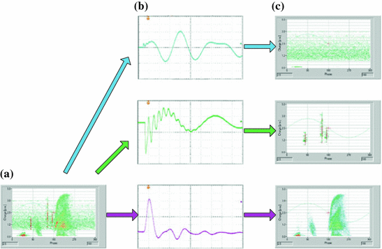
De-noising of PD signals using cluster separation according to Cavallini and Montenari (2007). a Acquired data stream captured during a testing time of 10 min. b Waveform analysis. c Cluster separation
In this context it should be emphasized that advanced de-noising tools can successfully be applied only by experienced test engineers, who must be familiar not only with the fundamentals of PD measurements but also with the operation principle as well as the capabilities and obstacles of the de-noising tools adopted. Even if sophisticated de-noising software is often implemented in advanced computerized PD measuring systems, it should not be overlooked that electromagnetic interferences can often simply be discriminated from PD pulses by means of multichannel digital oscilloscopes and thus conveniently be canceled using classical analogue features, such as windowing and gating, as discussed previously.
4.6 Visualization of PD Events

So-called Lissajous figure technique used since the 1960 s to display the charge of PD pulses occurring within a single cycle of the applied AC test voltage. a Voltage appearing across the measuring capacitance of an integrating bridge. b Traditional elliptical display mode

Oscilloscopic screenshots of phase-resolved PD patterns gained for needle-to-plane test samples under power frequency (50 Hz) AC voltage. a Discharges in air at inception voltage. b Discharges in air at test level substantially above inception voltage. c Cavity discharges in XLPE at inception voltage. d Surface discharges at inception voltage
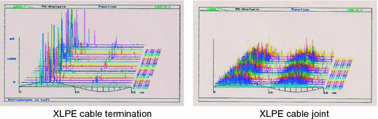
PD signatures of defective cable accessories displayed like waterfall diagrams
Today’s digital PD measuring systems acquire and store the vector ![$$ \left[ {q_{i} ;u_{i} ;t_{i} ;\varphi_{i} } \right] $$](../images/214133_2_En_4_Chapter/214133_2_En_4_Chapter_TeX_IEq117.png) for each captured PD pulse. Here are:
for each captured PD pulse. Here are:
-

the pulse charge of the individual PD current pulse
-

the instantaneous value of the applied test voltage
-

the instant of PD occurrence
-

the phase angle at instant of PD occurrence

Principle for displaying cumulative phase-resolved PD patterns

Using the replay-mode to visualize phase-resolved PD patterns originally acquired and stored in the computer memory in the course of development tests of stator bars of a hydro-generator visualized by the use of the replay-mode. a Long-term PD test under AC voltage (test level 18 kV, test duration 10 min, which equals 30,000 AC cycles). b Short-term PD test under enhanced AC voltage (test level 24 kV, test duration 2 min, which equals 6000 cycles)

Using the replay-mode to visualize phase-resolved PD pulses occurring within a single cycle of the applied 50-Hz AC test voltage (see cursor position obvious from the test voltage profile). a Elliptical time base. b Linear time base
 between the reference pulse “n” and the previous occurring pulse “n − 1”, as well as the associated voltage difference
  between the reference pulse “n” and the following pulse “n + 1”, is plotted in a graph displaying the value pairs
  versus
  . A measuring example for this is shown in Fig. 4.63b which refers to slot discharges detected in a rotating machine.
Principle of PD pulse sequence analysis (a) and measuring example (b) gained for cavity discharges in a power cable termination
standard deviation,
skewness,
kurtosis and
cross-correlation.

PD fingerprint of a discharge source recognized in a HV cable termination in service
Hn (phi): Number of PD pulses occurring within each phase window versus the phase angle,
Hq (phi)peak: Peak values of PD pulses occurring within each phase window versus the phase angle,
Hq (phi)mean: Mean values of PD pulses occurring within each phase window versus the phase angle. This quantity is deduced from the total charge amount within each phase window divided by the pulse number occurring in this phase window.

Comparison of the PD fingerprint gained for stator bar insulation with earlier established PD fingerprints gained for various test samples
4.7 PD Detection in the VHF/UHF Range
4.7.1 General
Performing PD measurements in compliance with IEC 60270:2000, the upper cut-off frequency has to be limited below 1 MHz, as recommended in the Amendment to this standard and discussed more in detail in Sect. 4.3. However, under this condition the signal magnitude is substantially attenuated, so that well shielded test laboratories are required to perform sensitive PD tests. Obviously, the signal-to-noise ratio can significantly be enhanced when the PD signal is captured in the VHF/UHF range. This non-conventional method has first been employed for quality assurance tests of gas-insulated substations by Fujimoto and Boggs (1981). Later the benefits of this approach has successfully been proven for on-site PD diagnosis tests of HV/EHV cable accessories (Pommerenke et al. 1995) and even for PD diagnostics of power transformers under on-site condition (Judd et al. 2002). Moreover, the capability and limits of the non-conventional PD detection in the VHF/UHF range has extensively been investigated by various CIGRE Working Groups. The main issues of these studies are summarized in the Technical Brochures No. 444 (2010) and No. 502 (2012). Based on these publications, the IEC 62478:2015 provides valuable recommendations for the design of VHF/UHF PD measuring systems including the sensors required to capture the PD transients radiated from the test object.
Due to the extremely wide frequency spectrum of PD pulses, which covers the ranges of radio frequency (RF: 3–30 MHz), very high frequency (VHF: 30–300 MHz), and ultra-high frequency (UHF: 300–3000 MHz), various kinds of PD couplers have been developed in the past, which are commonly classified as capacitive, inductive and electromagnetic sensors, as will briefly be presented in the following.
4.7.2 Design of PD Couplers
4.7.2.1 Capacitive PD Couplers
To capture the PD signal from the terminals of the test object, the classical coupling device recommended in IEC 60270:2000 provides a HV coupling capacitor connected in series with a measuring impedance. The upper cut-off frequency of such a coupling device (Fig. 4.66a) is commonly limited below 10 MHz, which is equivalent to a rise time close to 30 ns. To increase the upper limit frequency, it is necessary to decrease the value of the coupling capacitor, because this is associated with a reduction in the internal inductance, which determines the achievable upper cut-off frequency (Fig. 4.66b). Consequently, the highest measuring frequency is achievable by means of capacitive sensors providing a simple metallic disc. The feasibility of this simple approach has initially been proven for the detection and pinpointing of PD sources by means of a hand-held PD probe, as shown in Fig. 4.66c and described also in Sect. 10.4.4 (Fig. 10.43). Such kinds of capacitive sensors, often referred to as C-sensors, receive the electric field component of electromagnetic PD transients.
 between sensor electrode and inner cable conductor and lies in the pC range.
Step voltage response measured for capacitive PD couplers. a High-capacitive coupling capacitor designed according to IEC 60270:2000 (capacitance 2000 pF, rated voltage 24 kV). b Low-capacitive coupling device (capacitance 50pF, rated voltage 12 kV). c Disc-shaped C-sensors intended for PD probing (capacitance <5 pF)

Sketch of a capacitive PD coupler attached to a power cable
Example Consider a polyethylene-insulated power cable of dielectric permittivity of εr = 2.2. Assuming a ratio between outer and inner cable conductor of ra/ri = e ≈ 2.7, one gets for a coaxial C-sensor of length la = 100 mm the following approximation:


Here are Ip and tr the peak value and the rise time of the PD pulse current, respectively, and Zc is the characteristic impedance of the power cable. Assuming, for instance, a cavity discharge creates a current pulse of rise time tr = 1 ns and peak value Ip = 1 mA, one gets for the above-introduced circuit parameters (Cs = 12 pF, Zc = 30 Ω, Zm = 50 Ω) a detectable peak voltage of Vp = 18 mV, which is well measurable by means of digital oscilloscopes.
4.7.2.2 Inductive PD Couplers

L-sensor attached to a power cable termination

Set-up for measuring the step current response of inductive PD sensors (a, b) and oscilloscopic records gained for pulse transformers having n = 10 windings (c) resp. n = 1 winding (d)
4.7.2.3 Electromagnetic PD Couplers
 and the magnetic field component
  , as given by the Maxwell equations:

Sketch of an UHF sensor installed in a GIS flange

Operation principle of a pair of directional coupler sensors (DCS) installed at both sides of a power cable joint

UHF PD coupler based on the concept of transmission line inverters. a Equivalent circuit. b Technical design. c PD pulse response in the time domain recorded at time base of 1 ns/div. d Transfer function in the frequency domain

UHF-PD coupler attached to a GIS-cable termination. a Flexible PD sensor used for periodical PD monitoring. b Fixed PD sensor used for continuous PD monitoring
4.7.3 Basic Principles of PD Detection in the VHF/UHF Range

PD pulse response of the investigated UHF amplifiers (violet traces) and the associated peak detector (green traces). a Wide-band measuring system. b Narrow-band measuring system

Survey on UHF/VHF PD detection principles

Oscilloscopic screenshots gained by means of a spectrum analyser using the full-span mode (50–300 MHz). a Background noise level of the measuring surroundings. b Frequency response against a calibrating pulse
Using the full-span mode, the frequency spectrum of the captured PD signal as well as the superimposed noise is recorded for the pre-selected start and stop frequencies. To discriminate disturbing noises from the signal caused by PD events, the background noise level is initially recorded just prior the actual PD test is performed, see Fig. 4.76e. The main obstacle of the full-span mode is that the classical phase-resolved PD pattern cannot be displayed. To overcome this crucial problem, the zero-span mode is often preferred, which is in principle comparable with that technique used for radio interference voltage (RIV) measurements (Sect. 4.3.3). That means the center frequency is adjusted such that the noise level becomes a minimum, which can conveniently be determined using the full-span mode.
4.7.4 Comparability and Reproducibility of UHF/VHF PD Detection Methods

Oscilloscopic screenshots of phase-resolved PD pulses captured from a defective power cable termination which were measured simultaneously by means of a VHF measuring system (pink trace) and a PD instrument designed according to IEC 60270 (green trace). a Positive half-cycle. b Negative half-cycle

Results of comparative PD studies showing the magnitudes of the PD current pulses evaluated by the VHF method versus the magnitudes of the apparent charge pulses
Despite the drawback that the UHF/VHF PD detection method cannot be calibrated in terms of pC, there are also various benefits. So the signal-to-noise ratio is essentially enhanced if compared to the IEC method, as mentioned previously. This offers the opportunity to determine the PD inception voltage as well as the PD trend under noisy on-site conditions. Moreover, this technique can advantageously be used for the localization of potential PD defects in geometrical extended HV apparatus, such as GIS, using the time-of-flight measurement (Pearson 1991), as will be described in Sect. 10.4.1.
4.8 Acoustic PD Detection
PD events radiate not only electromagnetic waves but emit also acoustic pressure waves, where the acoustic signal covers a frequency range between some kHz and several hundreds of kHz. The main benefit of the detection of acoustic emitted (AE) waves is their immunity against electromagnetic interferences. To prevent an impact of other mechanical vibrations caused by pumps and fans as well as acoustic noises emanated from the iron core of transformers on account of magnetostriction and Barkhausen effect, commonly the ultrasonic frequency range, preferably between 40 kHz and few 100 kHz, is chosen to capture and acquire AE signals.

Photograph of an ultrasonic PD detector.
Courtesy of Doble Lemke
In the late 1950s, the ultrasonic PD detection technique was also employed to recognize and localize structure-borne noises emitted from PD defects in HV apparatus (Anderson 1956). Thereafter this technology became a widely established tool for preventive PD diagnostics of gas-insulated substations (Graybill 1974; Lundgaard et al. 1990; Albiez and Leijon 1991) and even for the localization of PD faults in large power transformers (Harrold 1975; Nieschwitz and Stein 1976; Howels and Norton 1978; Lundgard et al. 1989; Fuhr et al. 1993). Besides the magnitude, also the shape of the ultrasonic signal could be very informative to identify and localize potential PD defects due to the fact that the frequency content as well as the magnitude of the received acoustic signal appears considerably attenuated at increasing distance to the PD source.
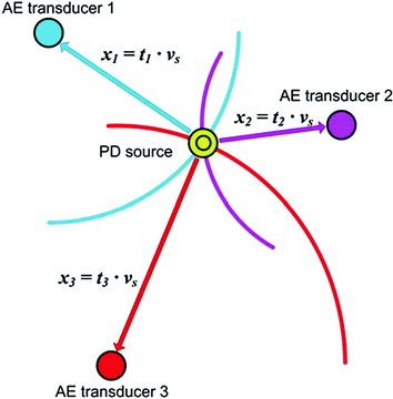
Principle of triangulation used for localization the PD site

Principle of time-of-flight measurement, where the acoustic signal is received by three ultrasonic transduces attached to the tank of a 110-kV instrument transformer. Here the oscilloscope was triggered by an electrical PD signal. a Single-pulse triggering. b Multi-pulse triggering (averaging)
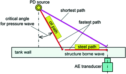
Shortest and fastest path between a PD source in oil and an acoustic sensor placed on a power transformer tank
Piezo-electric transducers,
Structure-borne sound resonance transducers,
Accelerometers,
Condenser microphones, and
Electro-optic transducers.
As the acoustic impedance of the transducers is very different from that of the metallic enclosure of the HV apparatus under investigation, the transducer surface is usually covered with hard epoxy resin to ensure an efficient signal transmission. This provides additionally the required insulation between transducer and metallic parts of the test object. Moreover, special attention should be paid to the coupling method due to the fact that the emitted acoustic wave might be reflected at the interface between transducer and the enclosure of the HV equipment. Thus, acoustic couplant gel or grease should be used to minimize the impact of reflections.

PD pulse response of a narrow-band ultrasonic measuring system having a center frequency of 42 kHz and a bandwidth of 800 Hz. a PD pulse train leading to a superposition of the acoustic signal. b Response of the acoustic measuring system against a single PD pulse