Chapter I.2.13
Surface Patterning
Introduction
Surface patterning is the use of surface modification methods to create chemically or physically demarcated regions on a surface. The art of patterning surfaces has a long history; the recent antecedent methods to pattern biomolecules are derived, in part, from the microelectronics industry (Xia and Whitesides, 1998; Whitesides et al., 2001; Geissler and Xia, 2004). As hand-wiring small, complex electronic devices became increasingly difficult, new methods were developed to pattern substrates such that many electrical components and interconnects between the different components of these devices could be created on the surface of a relatively large substrate in a batch process. These processes that have been instrumental to the development of all modern electronic devices have been driven by a set of technologies to create micro- and nanoscale features on the surface of semiconductors that are collectively and somewhat loosely termed “photolithography.”
Many of these surface patterning techniques, especially photolithography, have become important tools for biomedical research. The unique demands of biomedical research (for example soft hydrated materials such as proteins and hydrogels in an aqueous environment), impose a special set of demands and constraints on patterning methods. Seen from this broader perspective, it might be argued that the conceptual origins of many of the techniques used to pattern biomolecules on surfaces extend back to the pre-industrial era, to techniques that were developed to print on paper and textiles, such as block printing, screen printing, lithography, and batik.
This chapter focuses on surface patterning in the realm of biomedical research. The goal of this chapter is to familiarize the reader with various surface patterning techniques, and how these techniques can be used in biomedical research. First we discuss important figures-of-merit of patterning methods that allow different methods to be compared with each other, and allow a user to decide which patterning method is most appropriate for a specific application. Then, we discuss various types of patterning techniques, and follow up with a brief conclusion.
Some chapters in this textbook that provide background information for this chapter include I.1.5 (Surface Properties and Surface Characterization), I.2.10 (Non-Fouling Surfaces), and I.2.12 (Physico-Chemical Surface Modification of Materials Used in Medicine). However, as will quickly become apparent, this chapter has implications for many other chapters in the book.
Common Concerns in Biomolecular Surface Patterning
Surface patterning is carried out for a wide variety of reasons and, in turn, the ultimate goal of the patterned substrate defines a set of constraints or concerns that dictate how the fabrication process should be carried out. Surface patterning within the scope of biomaterials research is largely focused on the patterning of biomolecules or the patterning of cells. Listed below are important figures-of-merit (FOMs) and concerns that typically need to be addressed in patterning biomolecules or cells on solid substrates for a specific application. We also briefly discuss how the selection of an appropriate patterning methodology for a particular application is not usually influenced by a single FOM, but is usually dictated by the technique that offers the best combination of several FOMs.
Resolution
Resolution refers to the smallest feature size that can be reliably created by a patterning technique. Although the resolution of new techniques is constantly pushed towards smaller feature sizes and finer control, it is also useful to know what range of feature sizes a particular technique is capable of producing. Figure I.2.13.1 shows an example of different size patterns created with a high-resolution technique, as well as patterns created with a lower-resolution technique but one that is capable of a wider range of feature sizes. The highest resolution is not necessarily better, as the desired resolution depends upon the application. Thus, to pattern cells whose dimension are at least several micrometers, a technique with a relatively low resolution in the micrometers range is likely adequate, as long as it can pattern a large enough area, i.e., have a high enough throughput, which is discussed next.
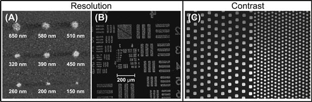
FIGURE I.2.13.1 Examples of Resolution and Contrast in Surface Patterning. (A, B) (Two “Resolution” images): features of different sizes created with a high-resolution patterning technique: (A) Lee et al., 2006a; and relatively lower-resolution technique: (B) Yang et al., 2000. (C) (Two “Contrast” images): the example in (C) represents a higher throughput process, since a large range of feature sizes and a larger surface area can be patterned in a one-patterning process. This is an example of high contrast due to patterning on a non-fouling surface that minimizes background signal (10 μm square features and 5 μm circular features) (Hucknall et al., 2009a).
(A) is adapted with permission from Wiley-Blackwell. (B) is adapted with permission from (Yang, Z., Frey, W., Oliver, T., & Chilkoti, A. (2000). Light-activated affinity micropatterning of proteins on self-assembled monolayers on gold. Langmuir, 16(4), 1751–1758). Copyright (2000) American Chemical Society. (C) is adapted and reprinted under the Open Access Creative Commons License with permission from the authors.
Throughput
While resolution refers to the smallest possible feature size that can be created by a patterning technique, throughput is a measure of the surface area that can be patterned in a given time. The throughput of a patterning technique is especially important for its use in manufacturing of devices where it is imperative that the patterned substrates can be produced on large length scales and on a timescale that is useful for manufacturing – minutes to hours, rather than days to weeks. Although the different types of patterning techniques are discussed later in this chapter, here we briefly discuss a few patterning methods to illustrate throughput considerations. Direct-write or “on-the-fly” types of patterning methods are those that use a stylus and ink to pattern a surface. These techniques usually provide precise control over the patterning process and finer feature sizes – often sub-100 nm – than some other printing methods such as microcontact printing, and can often create arbitrary feature shapes. Patterning large areas (i.e., greater than hundreds of square micrometers) rapidly, however, is challenging for most variants of this type of patterning. On the other hand, techniques based on printing using a stamp can readily pattern large areas of a surface quickly (in the order of seconds to minutes), but may only be able to access certain shapes of features (e.g., circles, lines or squares), and may have limited resolution (i.e., on the micrometer scale or greater).
Contrast
Contrast is the degree to which the components in the pattern are distinguishable from the background substrate (Figure I.2.13.1). In many surface patterning methodologies, contrast is achieved by patterning one material on the surface of another material. In patterning biomolecules, however, contrast is usually defined as the surface density of the deliberately patterned biomolecule of interest relative to other biomolecules that might adventitiously be bound to the background regions of the same surface, as a consequence of the patterning method. Contrast in patterns of active molecules, such as enzymes or antibodies, can be assessed by measuring the activity of the patterned molecules after the patterning process. For example, enzyme patterns can be visualized by monitoring the concentration of insoluble fluorescent products created by the enzyme (usually via their fluorescence intensity) from the patterned regions relative to the unpatterned background regions when incubated with a soluble, non-fluorescent enzyme substrate. Another example of biomolecular patterning in which the activity of the patterned molecule can be used to measure the contrast is when the patterned molecule has an affinity for another molecule, as is the case for antibody/antigen and many protein–ligand interactions (e.g., avidin-biotin). Here, contrast can be visualized by exposing the pattern to a complementary target molecule containing a fluorescent, radioactive or plasmonic tag that enables visualization of the pattern.
In rare cases, biomolecular patterning involves molecules with a functional activity or activity that is difficult to assess in a purely in vitro setting. In these cases, pattern contrast is often visualized by exposure to a secondary processing step for pattern visualization. For example, contrast in patterned peptides that act as cues for cell adhesion can be visualized by exposing the pattern to cells in culture, and the degree of cell patterning is an indirect measure of the fidelity and contrast of the pattern.
Contrast in biomolecular patterning is heavily dependent on surface properties of not only the pattern itself, but also of the background. Biomolecular patterns are often exposed to solutions that can contain complex mixtures of proteins and other molecules in the course of their use, and most surfaces are particularly prone to nonspecific and irreversible adsorption of proteins. Removing nonspecifically adsorbed proteins requires the use of detergents or other harsh conditions that are typically not suitable for many biological applications. Thus, maintaining contrast in biomolecular patterning usually involves some sort of passivation step to prevent two sets of undesirable events: (1) adsorption of the molecule to be patterned on the unpatterned background regions; (2) adsorption of biomolecules – that are to be subsequently exposed to the patterned surface – onto the patterned features or the background regions of the surface (Figure I.2.13.2).
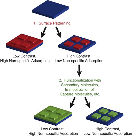
FIGURE I.2.13.2 Contrast and Non-Specific Adsorption. Maintaining contrast during patterning of biomolecules often requires that: (1) the patterned materials have low non-specific adsorption to the background substrate; and (2) that any molecules used in subsequent steps (functionalization of pattern with secondary, reporter molecules; immobilization of antigens or capture molecules from solutions; etc.) also have low non-specific adsorption to the background
Non-specific adsorption can be reduced by methods of varying degrees of complexity (also see Chapter I.2.10). Perhaps the most common and simplest way to reduce non-specific adsorption is to use proteins that adsorb to surfaces, such as bovine serum albumin (BSA), under the assumption that controlled deposition of a surface-active protein will prevent the immobilization of most other molecules to the substrate. However, adsorption of BSA often leads to sub-monolayer coverage of the surface, and it has been shown that proteins can adsorb to a BSA layer (Hyun et al., 2001), so that this strategy, despite its widespread use, is of limited utility.
A more effective way of reducing non-specific adsorption is to create a “non-fouling” surface. Non-fouling surfaces are typically defined as surfaces that have a molecular or polymer layer that prevents the adsorption of proteins on a surface. A common method to create a non-fouling surface is to form a dense layer of polyethylene glycol (PEG) on the surface. Here, the network of ethylene glycol molecules effectively creates a hydrated barrier between the bulk solution and the solid surface. Proteins in solutions can diffuse into and out of the network without becoming immobilized to the surface. The degree of protein resistance is related to the density of PEG molecules on the surface (Ma et al., 2006a; Hucknall et al., 2009a; Zauscher and Chilkoti, 2009). Unfortunately, most methods to adsorb PEG or chemically attach it to the surface (Lee et al., 1989; Amiji and Park, 1993; Llanos and Sefton, 1993; Prime and Whitesides, 1993; Elbert and Hubbell, 1998; Liu et al., 2002; Xia et al., 2002; Bearinger et al., 2003) do not provide a high enough density of oligoethylene glycol moieties on the surface. In these cases the PEG will decrease, but will not eliminate the adsorption of proteins, especially from highly complex and concentrated protein mixtures such as serum and plasma.
In situ polymerization methods, also termed surface-initiated polymerization, in which an initiator is tethered to a surface and a PEG-like coating is directly grown from the surface, are a powerful method to grow a dense layer of a polymer that presents a high density of oligoethylene glycol moieties at the surface. Such surfaces are highly resistant to protein adsorption (Ma et al., 2004, 2006a,b; Hucknall et al., 2009a,b,c; Zauscher and Chilkoti, 2009), and patterns made on these non-fouling surfaces remain functional for extended periods of time in cell culture (Ma et al., 2004).
Other methods that are also useful to create non-fouling interfaces include self-assembled monolayers of alkanethiols that present an oligoethylene glycol moiety at the solid–water interface (Prime and Whitesides, 1993; Herrwerth et al., 2003), inter-penetrating polymer networks that present PEG at their solvent interface (Bearinger et al., 2003), plasma-deposited “PEG-like” films deposited from oligoglyme precursors (López et al., 1992), and the deposition of PEG-poly(lysine) (PEG-PLL) by electrostatic adsorption (Kenausis et al., 2000; Huang et al., 2001). However, some of these methods are somewhat limited in their utility across a range of polymer substrates. For example, PEG-PLL is only useful for negatively-charged surfaces, and has typically been most successful with metal oxide surfaces that have a negatively-charged surface, while oligoethylene glycol-terminated self-assembled monolayers (SAMs) are only applicable to gold and silver.
Bioactivity
Preserving the bioactivity of a biomolecule during the patterning process is a significant and non-trivial concern. Many patterning processes, especially those that are adapted from the semiconductor processing industry, can involve exposure of the surface to extreme environments, such as high vacuum, extreme temperatures, and non-aqueous conditions, which can denature or degrade biomolecules. Methods that are compatible with aqueous conditions and ambient temperature are hence preferable when deciding upon a method to pattern a biomolecule – especially proteins – on surfaces, as they are especially prone to denaturation compared to other biomolecules such as peptides and oligonucleotides.
Shelf-Life and Durability
The shelf-life and durability of the pattern over time is another consideration when choosing a patterning methodology. This is especially important in the case where patterns need to be generated for use in diagnostic or point-of-care devices. The ultimate convenience in such a situation would be one where a fully functional pattern can be manufactured, stored in ambient conditions for an unspecified amount of time, and then used by the end-user. These conditions can easily be met when patterning “hard” materials, such as those used in microelectronics, because they are typically not very sensitive to their environment. However, when “soft-wet” materials – hydrated polymers, proteins, and cells – are patterned, the exposure of these materials to vacuum, high temperature or extremes of pH becomes a critical and often limiting issue, because many of these materials are easily degraded, destroyed or irreversibly denatured under these conditions. For this reason, special care is needed to ensure that all biological components involved in the patterning process are maintained in a functional state. Ensuring this may involve strategies such as sealing the devices in a hydrated environment so that they are protected from the environment until they are ready for use, using preconditioning steps to prepare the surface prior to analysis or integration of rinsing steps into the analysis scheme. In some instances it may be necessary to create the patterned substrates that act as a template for patterning biomolecules, and then functionalizing the pattern with the biomolecule of interest, on demand, immediately prior to its use. An example of this approach would be the fabrication of a pattern of a non-fouling polymer on a substrate, which can be stored for an extended period of time under ambient conditions. Immediately prior to use, hydration of the surface and incubation in a protein solution drives adsorption of the protein only to the unpatterned regions, leading to the spontaneous formation of a protein pattern driven by the thermodynamic template on the patterned surface. This approach has the advantage of obviating the need to store the surface in a hydrated environment, which would have been necessary if the surface had been patterned with a protein at the outset, rather than on-demand.
In addition, it is also useful to know how long a pattern will stay patterned under the end-use conditions. This is especially important for substrates patterned for cell growth or for implantation into the body that need to retain functionality for extended periods of time. For this reason, researchers will often report an FOM that alludes to the life of the pattern by stating, for example, how long the cells remain confined to the pattern in cell culture.
Patterning Techniques
The number of different surface patterning techniques increases daily, with new publications that present novel patterning schemes or variants of existing methodologies. This chapter seeks to provide a short discussion of the different categories of patterning techniques, and within each category points out some interesting examples; this chapter is not an exhaustive compendium of all patterning techniques.
Much of the overall organization or structure of this section owes an intellectual debt to the excellent and comprehensive review by Geissler and Xia (2004). However, the content of this section places greater emphasis on patterning for biomedical applications. We first present direct-write patterning techniques; these techniques typically provide high resolution at the expense of speed and throughput. Presented next are mask- and master-based patterning techniques, which provide high throughput and can pattern large surface areas, but often have lower resolution compared to direct-write techniques. Next, patterning by self-assembly is described, which is a powerful technique for patterning large surface areas with high-resolution features by exploiting intermolecular interactions. We also present a brief section on the use of dynamic patterning for interrogation of biological environments. Finally, we conclude with a few examples of three-dimensional patterning techniques that can be used to control the three-dimensional microenvironment of cells.
Direct-Write Patterning
In direct-write patterning techniques, patterns are fabricated by serially scanning a patterning element across a substrate. Direct-write patterning is a useful method because patterns of arbitrary feature shape and size – within the resolution limit of the technique – can be fabricated on-the-fly, in a process analogous to writing with a pen. In addition, direct-write patterning can generate extremely high-resolution features with great spatial accuracy. The drawbacks of direct-write patterning techniques are that they are typically slow, low-throughput, and not particularly suitable for large area patterning, because of the need to serially write the pattern. This limitation can be addressed, at the cost of greatly increased complexity of the instrumentation, by using independently actuated pens. Several direct-write techniques are described next and are grouped by the type of “pen” that is used to write the pattern (Figure I.2.13.3).
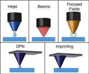
FIGURE I.2.13.3 Types of Direct-Write Patterning. Inkjet, beams, focused fields, dip-pen nanolithography (DPN), and imprinting.
Writing with a Stylus
This section describes direct-write patterning techniques that use a rigid stylus to write the pattern. Dip-pen nanolithography (DPN), nanoimprinting, and nanoengraving (also called nanoshaving) are typical direct-write methods that use tips under control of an atomic force microscope (AFM) to write the pattern. Very fine AFM tips are available, and AFMs have nanometer positional control, thus, DPN, nanoengraving, and nanoshaving can all produce very high-resolution, sub-100 nm features. In contrast, inkjet printing produces coarser features, with the best lateral resolution of ~10 μm, and more often in the order of 100 μm. Inkjet systems, however, can be easily multiplexed, making them very attractive for patterning biomolecules in diagnostic devices, such as protein and DNA microarrays.
Printing with Inkjets, Quills, and Pins
Inkjet printing refers to any method where liquid is pumped through a nozzle and onto a substrate in a defined pattern. Inkjet printers deliver liquid solutions as small droplets – typically 10–20 pL in volume (Geissler and Xia, 2004) – that are either continuously pumped through the nozzle head, electrostatically charged, and then guided via electric fields or generated on demand by thermally or mechanically triggered pressure pulses (Derby, 2008). The liquid inks are typically stored in reservoirs and pumped into the printer as needed. Inkjet nozzles are usually very small (20–30 μm in diameter) (Geissler and Xia, 2004), which enables them to be mounted on nozzle heads that can be interfaced with computers to control the fabrication of patterns. The resolution limit of inkjet printing is in the range of tens of micrometers, and is limited by the droplet volume, droplet spreading on the substrate (which varies depending on the ink and the surface), and other mechanical factors. Some useful features of inkjet printing are: (1) patterning is contact-free and can be performed under ambient conditions on a range of solid substrates; (2) the method has high positional accuracy; (3) multiplexed printing of analytes is easily accomplished by use of multiple nozzles and/or nozzle heads; and (4) high-throughput patterning over large surface areas can be accomplished by robotic automation.
Inkjet printing of biomolecules has gained popularity in recent years, in part due to the simplicity of the technique and the widespread availability of cheap printers. Thomas Boland’s research group demonstrated that low-cost consumer inkjet printers could be adapted to print “biological inks” with their demonstration of the inkjet printing of proteins (Pardo et al., 2003), live cells (Xu et al., 2005, 2006a), and bacterial colonies (Xu et al., 2004). Figure I.2.13.4 shows a “living advertisement” – a colony of bacteria printed in the shape of a university logo – printed by Boland and co-workers.
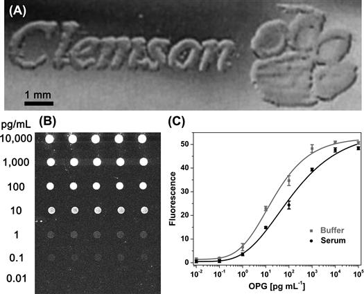
FIGURE I.2.13.4 Inkjet Printing. A colony of bacteria printed in the shape of a university logo by a modified consumer-grade inkjet printer (A) (Xu et al., 2004). An inkjet printed antibody microarray on a non-fouling surface (B) is used for ultrasensitive detection in complex mixtures such as blood and serum (C) (Hucknall et al., 2009c).
(A–C) are adapted/reprinted with permission from Wiley-Blackwell.
Automated robotic inkjet printing systems designed to print “biological inks” such as DNA or proteins are typically called microarray printers, and are much more sophisticated and expensive than consumer-grade inkjet printers. These systems are often self-contained in an environmentally controlled chamber, and can run complex protocols involving delivery of multiple solutions as well as rinsing steps. Such systems are used to create spatially addressable arrays of biomolecules, such as DNA microarrays (Marshall and Hodgson, 1998; Bier et al., 2008). However, much of this work used arrays fabricated not by inkjet printers, but by pin-based arrayers in which pin arrays are dipped into solutions and then contact printed onto a surface (DeRisi et al., 1997), or else arrays that were fabricated by on-chip, photolithographic synthesis of spatially addressable arrays of oligonucleotide probes, such as the Affymetrix oligonucleotide array technology (Fodor et al., 1991). Since the advent of the human genome project and the rise of genomics, microarrays have migrated into other fields because they provide a convenient, high-throughput, and multiplexed methodology to characterize biomolecules. For example, protein arrays are used in proteomics (Caiazzo et al., 2009), and have been used to identify protein markers for disease (Orchekowski et al., 2005). Pin-based arrayers have also largely been used to fabricate protein arrays (MacBeath and Schreiber, 2000; Ray et al., 2007), because it is significantly cheaper and less complex to manufacture arrayers with a large number of pins or quills, compared with scaling-up the number of independently actuated inkjets beyond a dozen. Similarly, both pin-based (Pilobello et al., 2005, 2007; Pilobello and Mahal, 2007) and inkjet microarrays (Nagaraj et al., 2008) have been used to fabricate lectin arrays for glycomics. Microarrays have also been used as clinical diagnostics to detect specific analytes (Delehanty and Ligler, 2002; Hucknall et al., 2009c). For example, the Chilkoti group has used inkjet printed microarrays of antibodies on a non-fouling polymer brush for the detection of multiple protein analytes from serum and blood with a femtomolar limit-of-detection (Hucknall et al., 2009c) (Figure I.2.13.4).
Dip-Pen Nanolithography (DPN)
DPN is the nanoscale equivalent of writing with a quill. In DPN, AFM probes are inked with a solution of molecules and then scanned along a surface to write a pattern of the ink. The ink solution forms a small meniscus between the tip of the probe and the surface, which transports biomolecules from the tip to the surface. DPN has been used to pattern alkanethiols (Hong et al., 1999; Piner et al., 1999), as well as a range of biomolecules including DNA (Demers et al., 2002), proteins (Lee et al., 2002, 2006a), functional enzymes (Hyun et al., 2004a), biopolymers (Hyun et al., 2004b), and viruses (Vega et al., 2005) on many different materials. The resolution limit of DPN is on the order of tens of nanometers, and this method can create patterns that extend over several hundred micrometers, which is the limit of most AFM scanners. Single probe DPN patterning is also relatively low-throughput, as it is a somewhat slow and serial patterning technique. For example, in an early report on DPN (Piner et al., 1999), 10 minutes were required to create a 1 μm × 1 μm feature.
High-throughput DPN can be performed by mounting multiple probes on a single scan head. Perhaps the most impressive work to date in this regard is that of Chad Mirkin’s group, where 55,000 DPN probes were inked with a thiol solution, and used simultaneously to generate massively high-throughput, high-resolution patterns (Figure I.2.13.5A) (Salaita et al., 2006). In this demonstration, the face of Thomas Jefferson from a US five-cent coin was generated 55,000 times, with each face containing 470 million nanoscale features, in less than 30 minutes (Figure I.2.13.5B). Commercial DPN systems are now available that are capable of multi-probe patterning of nanoscale-to-microscale patterns over areas as large as 40 mm2 (NanoInk, Inc.). For good reviews of DPN, see Krämer et al. (2003), and Mendes et al. (2007).
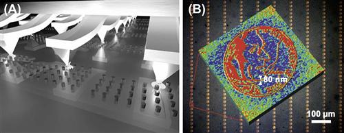
FIGURE I.2.13.5 High-throughput, high-resolution dip-pen nanolithography. For details of figures (A) and (B) please see the text. (Salaita et al., 2006).
Adapted with permission from Wiley-Blackwell.
Imprinting/Engraving
Nanoscale imprinting and engraving of surfaces can be accomplished by indenting or scraping a surface with a hard stylus, such as an AFM probe. Such techniques have similar advantages and limitations as DPN, as the patterning mechanism is very similar. Nanoshaving is a term used to describe the process of scratching patterns in thin molecular layers, such as SAMs, on a bulk substrate (Liu et al., 2000). Here, arbitrary patterns in the molecular layer are engraved by dragging the probe on the surface. A two-step process can be used to functionalize the exposed, underlying substrate with a secondary molecule. For example, nanoshaving has been used to selectively degrade a protein-resistant SAM on gold, which was then exposed to a solution of an antibody (Kenseth et al., 2001). Nanopatterns of antibodies were formed on the surface as the antibodies adsorbed to the exposed regions of the substrate that were no longer protein resistant. Nanografting – a variant of nanoshaving – involves scratching the surface in the presence of a secondary molecule with high affinity to the underlying substrate (Xu and Liu, 1997; Liu et al., 2000) so that the secondary molecule fills in the regions that are cleared away by the scanning probe. Nanografting has also been used to create nanopatterns of enzymes, antibodies (Wadu-Mesthrige et al., 1999, 2008; Hu et al., 2005), and DNA (Liu et al., 2002) on a surface.
Writing with Beams
This section describes patterning methods that scan an energetic beam over a surface to create a pattern. The spatial resolution of this class of patterning techniques is generally limited by the spot size of the beam. Beams of photons are used for patterning in direct-write photolithography, and thus the spot size (and hence, resolution limit) is set by the optical diffraction limit, which is ~200 nm. However, the diffraction limit can be overcome by using near-field methods, such as scanning near-field lithography, to create features in which the smallest dimension is ~tens of nanometers. Direct-write photolithography is particularly conducive to patterning biomolecules, as these methods are compatible with aqueous conditions. Electron beam lithography and focused ion beam lithography represent two other methods in this class of patterning techniques that have higher spatial resolution than conventional far-field photolithography. In these methods, shorter wavelength radiation is used than in photolithography, which leads to smaller spot sizes, and hence higher lateral resolution. Electron beam lithography and focused ion beam lithography, however, usually require high vacuum and dry samples, which can be a serious impediment to patterning biomolecules.
Direct-Write Photolithography
In direct-write photolithography, a beam of focused light is used to pattern a substrate directly. Here, light is usually focused into small spots using conventional light optics, and patterns are formed by photochemical or physical modification of the surface. The resolution of features patterned with conventionally focused beams of light is governed by the optical diffraction limit, which is roughly half of the wavelength of the light used for excitation (Dunn, 1999). Thus, patterns formed by focused light typically have a minimum feature size of several hundred nanometers. Feature sizes can be scaled upwards using larger spot sizes; however, intensity requirements of the patterning process or the amount of light-per-area necessary to form patterns, can in some cases be a limiting factor in producing larger features, as light intensity decreases with larger spot sizes. Although broadband light sources can be used for direct-write photopatterning, lasers are more commonly used for this application, because they provide high-intensity beams of a single wavelength which allows precise control of specific photochemical reactions.
Patterning with light is generally performed using a photochemical mechanism or a mechanism that induces a spatially localized physical change in the underlying substrate. In direct-write patterning via photochemistry, light is used to locally activate photoactive molecules that subsequently either form a pattern directly or react with another species to form a pattern. In some cases, the activated species is created in one step, and then another step is necessary to expose the activated species to the biomolecule to be patterned. However, in other cases the photoactivated species is generated in the presence of the secondary species to be patterned, and thus the pattern is created in one step. Another one-step patterning scenario is the case where the photoactive molecule is covalently attached to the molecule to be patterned. Photochemical patterning with light has been widely used to create patterns of proteins on a substrate. For example, Holden and Cremer used a laser to pattern enzymes directly within flow channels (Holden et al., 2004) (Figure I.2.13.6A), a methodology that can be applicable to lab-on-a-chip devices.
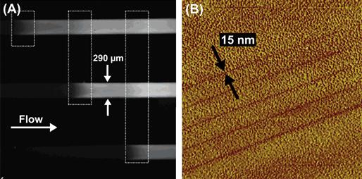
FIGURE I.2.13.6 Examples of Direct-Write Protein Patterning with Light. (A) Patches of enzymes (locations indicated by dashed boxes in the figure) patterned within flow channels produce fluorescent products when exposed to fluorogenic reagents; (B) Sub-diffraction limit features patterned with light using near-field excitation. Here, 15 nm lines were written in a self-assembled monolayer on gold (Ducker et al., 2007b).
(A) is adapted with permission from (Holden, M. A., Jung, S. -Y., & Cremer, P. S. (2004). Patterning enzymes inside microfluidic channels via photoattachment chemistry. Anal. Chem., 76(7), 1838–1843). Copyright (2004) American Chemical Society. (B) is adapted with permission from the authors and SPIE.
In the second methodology to pattern biomolecules using light, a laser is used to pattern substrates by physically altering a spatially localized region of a substrate. This type of patterning is conceptually similar to engraving with AFM tips, with the only difference being that the substrate material – polymers or resins – are ablated, melted or deformed due to the high energy of the focused laser spot, instead of being physically excavated (Joglekar et al., 2003). For example, Nielson and Shear used a high-energy pulsed laser to ablate pores in a membrane separating adjacent flow cells (Nielson and Shear, 2006). They showed that this technique could be used to dose cells with precisely located chemical gradients. In another example, the Yasuda group used a focused laser to photothermally etch microchambers in agar for use in single cell experiments (Kojima et al., 2003; Sugio et al., 2004; Suzuki et al., 2004).
Patterning with light can be used to create feature sizes that are much smaller than those created using diffraction-limited optics. An example of ultra-small direct-write photolithography is patterning by scanning near-field photolithography (SNP) that uses a near-field scanning optical microscope (NSOM) to create nanoscale patterns using light in the near field. In SNP, light is passed through a metal-coated optical fiber that is tapered to a ~50 nm aperture at its end that acts as a sub-wavelength light source. When in ~10 nm (Betzig and Trautman, 1992; Wegscheider et al., 1995) proximity to a photoactive substrate, the light source can excite chromophores in the near-field via the non-diffracting evanescent field that emerges from the tip, and thus can create patterns that are well below the diffraction limit. Leggett and co-workers have extensively used this technique to create nanoscale patterns of proteins and self-assembled monolayers (Sun et al., 2002; Sun and Leggett, 2004; Ducker and Leggett, 2006; Ducker et al., 2007a,b) (Figure I.2.13.6B).
Electron Beam Lithography
Direct-write electron beam lithography (EBL) uses similar patterning principles as that of patterning with focused light. However, in EBL, a focused beam of electrons (e-beam) is used as the stylus to write patterns in an e-beam sensitive material. The focused energy from the e-beam can initiate cross-linking (Brough et al., 2007; Christman et al., 2009) or functionalization (Eck et al., 2000; Golzhauser et al., 2001; Schmelmer et al., 2007; Steenackers et al., 2007) of surface moieties on the substrate. Since the e-beam radiation is of a much shorter wavelength than that used in direct-write photolithography, the spatial resolution of EBL is greater than direct-write photolithography. For this reason, EBL is a very powerful technique for creating patterns at the nanoscale, with feature sizes of 10–100 nm easily fabricated by EBL (Ducker et al., 2008). EBL, however, has several limitations: first, although existing scanning electron microscopy (SEM) systems can be easily configured for EBL, they are expensive, so EBL is not a routine technique that can be set up in a laboratory, and hence requires access to a dedicated instrument that is typically located in a shared instrumentation facility. Second, EBL requires high vacuum, which limits its utility for patterning biological molecules. Third, EBL is slow and can only pattern relatively small areas, although larger areas can be “stitched together” by moving the substrate using a motorized stage. The high resolution, low throughput, and high cost make EBL useful largely as a method for high-resolution fabrication of nanoscale patterns over a small area. As biological molecules generally do not remain functional in high vacuum, and are easily damaged by e-beam radiation, substrates are typically first patterned by EBL and then exposed to a biological molecule of interest for selective attachment of the biomolecule to the patterned features. An elegant example of patterning by EBL is the work done by Heather Maynard’s group, where multi-component protein patterns were fabricated by e-beam cross-linking of functionalized PEG molecules. These functional PEG patterns were then used to immobilize proteins from solutions via specific binding interactions between the proteins and the ligands presented by the PEG patterns (Christman et al., 2009) (Figure I.2.13.7, left).
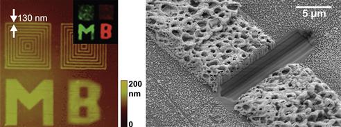
FIGURE I.2.13.7 Examples of EBL (left) and FIB (right) Patterning. Shown on the left is an example of EBL where multi-component protein patterns were formed by electron beam cross-linking and subsequent functionalization of poly(ethylene glycol) molecules. Shown on the right is an example where FIB milling was used to open a conductive circuit by milling a gap in a metallized protein-based wire (scale bar 5 μm).
(Left) is adapted with permission from (Christman, K. L., Schopf, E., Broyer, R. M., Li, R. C., Chen, Y., et al. (2009). Positioning multiple proteins at the nanoscale with electron beam cross-linked functional polymers. J. Am. Chem. Soc., 131(2), 521–527.). Copyright (2009) American Chemical Society. (Right) is adapted with permission from (Hill, R. T., Lyon, J., Allen, R., Stevenson, K., & Shear, J. B. (2005). Microfabrication of three-dimensional bioelectronic architectures. J. Am. Chem. Soc., 127(30), 10707–10711). Copyright (2005) American Chemical Society.
Focused Ion Beam
A focused ion beam (FIB) can also be used for direct-write patterning. FIB patterning is similar to EBL in its advantages and limitations; however, FIB patterning makes use of high-mass ions, such as gallium ions, as the energetic particles instead of electrons as in EBL. FIB patterning is an inherently destructive process, as the bombardment of a surface with ions causes atomic sputtering of atoms from the surface. For this reason, FIB is typically used as a milling technique to engrave a surface with submicrometer size features. For example, Hill et al. used an FIB to open a conductive circuit by milling a gap in a metallized protein-based wire (Hill et al., 2005) (Figure I.2.13.7, right). FIB can also be used to sputter metals (Reetz et al., 1997) onto a surface, which makes FIB useful in repairing integrated circuits (Geissler and Xia, 2004).
Writing with Fields
Direct-write patterning with fields includes scanning electric and magnetic fields across a substrate to form a pattern. Features generated by direct-write electric field scanning typically have a lower spatial resolution than that attainable with other direct-write techniques. Similar to other scanning techniques, writing with fields is slow and is unsuitable for large area patterning. However, scanning electrodes allow one to perform extremely localized electrochemical reactions. Direct-write magnetic patterning is mostly geared towards data storage and, as it has not been used for sputtering biomolecules, only the underlying principle will be briefly described in this section.
Electric Field
Direct-write patterning with electric fields is accomplished by scanning an electrode near a surface to locally modify the surface using charge or current. Patterning is mediated through a variety of electrochemical processes, which include localized charging, ohmic heating, and redox reactions. Scanning electrochemical microscopy (SECM), which was developed by Allan Bard and co-workers, can be used in a patterning mode to perform localized redox reactions on a surface, resulting in the formation of microstructures (Bard et al., 1990). SECM patterning is performed with ultramicroelectrodes in electrolyte solutions, and has been used to pattern enzymes (Shiku et al., 1997; Wittstock and Schuhmann, 1997) and SAMs on a surface (Wittstock et al., 1997). The feature sizes of patterns generated by SECM are typically larger than those created with other types of scanning probe techniques (Geissler and Xia, 2004). Scanning tunneling microscopy (STM) and AFM can be used to generate higher resolution features. STM has the highest resolution of all proximal-probe lithography methods, as it can manipulate single atoms (Eigler and Schweizer, 1990; Manoharan et al., 2000), but as it must be used under high vacuum to achieve atomic resolution, it is of limited utility for biomolecular patterning. Anodization lithography is a methodology in which biased AFM tips are used to selectively grow oxide nanostructures on a silicon oxide substrate (Ducker et al., 2008). Stefan Zauscher’s group has used anodization lithography to localize polymerization precursors, which were subsequently used to create nanopatterns of polymer brushes (Lee et al., 2006b).
Magnetic Field
Direct-write patterning with magnetic fields has mostly been geared towards data storage applications to date, and thus this topic will not be covered in detail in this section other than to provide the reader a basic idea of its underling physical principle. In direct-write magnetic patterning, an inductive element is scanned above a magnetizable material, such that localized regions of the surface become magnetized. These local magnetized areas allow data to be recorded as bits, and can read the stored data using the same type of inductive element that is used to generate the patterns. For more information on magnetic direct-write patterning, see the review papers by Chou (1997) and Geissler and Xia (2004). Magnetic patterning by self-assembly is discussed in a later section of this chapter.
Patterning with Masks
Patterning with masks is a highly developed form of patterning, as it has been the core technology of the microelectronics industry. Because of its sophistication and maturity, it has also been adapted for the patterning of biomolecules and cells. A mask is broadly defined as a template that can spatially modulate a field or radiation that passes through it, or a template that physically masks spatially defined regions of the underlying substrate from exposure to inks or etchants. Masking light to create patterns on substrates is the most common form of patterning with masks. Patterning with light and masks is generally called photolithography, even though photolithography can be performed in a mask-less, direct-write manner, as described previously. Mask-based patterning can also be performed with radiation (other than light), liquid inks or with chemical or biological etchants. Mask-based patterning is powerful and versatile for the following reasons: (1) large areas – typically 4–6 inch wafers – can be rapidly patterned in batch mode, which makes it a high-throughput patterning technique; (2) spatially intricate patterns can be fabricated that are only limited by the design of the mask; and (3) layered features can be fabricated by performing multiple patterning steps in succession, each with a different etching or deposition step. With advances in light sources and optics, the spatial resolution of mask-based approaches is now in the sub-200 nm regime (Totzeck et al., 2007).
Photolithography with Masks
In photolithography, a mask can be any material that has optically transparent and opaque regions. Masks can be rigid, such as those fabricated out of metal or printed on quartz glass, or they can be fabricated on flexible substrates such as transparencies. The critical requirement of a mask-based photolithographic patterning process is that light must pass through spatially defined regions of the mask and lead to the formation of a pattern that conforms to or is dictated by the pattern of the mask, on a substrate that is located below the mask. However, historically, the term photolithography encompasses a set of processes that derived from the semiconductor industry, which involves more than simply using light and masks to fabricate patterns.
In photolithography, patterning is facilitated by a polymer photoresist that is spin-coated onto a silicon wafer, activated by light, and developed in a developing solution (Figure I.2.13.8) to create a pattern of the photoresist, which is then subsequently processed to create a pattern in the underlying substrate. There are two types of photoresists. (1) A positive photoresist becomes soluble in the developing solution in areas that are exposed to light, while the unexposed regions of the photoresist are insoluble in the developing solution. After exposure and development, the areas of the positive photoresist that were exposed to light are dissolved and rinsed away to expose the underlying substrate. (2) A negative photoresist works on the opposite principle; areas of the photoresist that were exposed to the light will become less soluble in the developing solution, so that incubation in the developing solution will dissolve the unexposed regions of the photoresist, and expose the underlying substrate. The photolithography process is completed by removing parts of the exposed or unexposed photoresist. Removal is usually followed by an etching step in which the exposed thin metal/oxide films coating a bulk substrate are dissolved or a deposition step in which metal or other materials are preferentially deposited on to exposed regions.
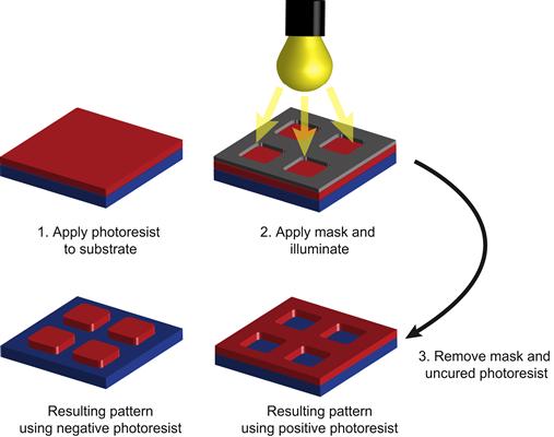
FIGURE I.2.13.8 Mask-Based Photolithography.
A mask can be placed relative to the light source and substrate in three modes: contact mode; proximity mode or projection mode. In contact mode, the mask is placed directly on the substrate. Contact mode photolithography produces features at a 1:1 size relative to the feature size in the photomask, and thus resolution is limited by the feature size of the photomask. In contact mode, it is essential that the substrate and mask are free of particulate contaminants, as any trapped debris between the mask and substrate will contaminate the pattern and/or damage the mask or substrate. Proximity mode patterning is a variant of contact mode, in that the mask is slightly separated from the substrate along the propagating light axis. Proximity mode photolithography also produces features in the substrate that are the same size as are patterned on the mask, but the presence of foreign contaminants is not as devastating as in contact mode, as the mask and the substrate are not in contact. In projection mode photolithograpy, the mask is placed at an image plane that is well separated from the surface of the substrate along the optical axis that is conjugate to the image plane at the surface to be patterned. Projection mode photolithography can produce a smaller feature size than is embedded in the mask, as optics can be used to project the mask pattern at very small physical dimensions. For example, a microscope can be used to reduce the mask pattern 100 times by using a 100 × microscope objective. Projection mode photolithography also enables higher-throughput processing, as mask alignment can be done quickly and efficiently due to reduced risk of damaging the mask or the substrate because they are well separated.
Typical photolithography with masks, as developed in the microelectronics industry, involves specialized photoresists composed of polymers that are designed to polymerize or depolymerize upon exposure to UV light. However, light-based patterning with masks can be accomplished with any material that is light responsive. An extreme example is mask-based patterning of bacteria in plates of agar by Levskaya et al., (2005). Here, bacteria were genetically engineered so that lacZ gene expression, which encodes β-galactosidase, could be repressed by light exposure. Photomasks were used to spatially localize lacZ gene expression, and hence β-galactosidase, to areas within the bacterial colony that were masked from light. Patterns were visualized by testing for β-galactosidase activity within the bacterial colony using media that formed black precipitates in the presence of β-galactosidase (Figure I.2.13.9).
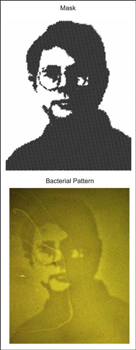
FIGURE I.2.13.9 Projection Mask Photolithography of Bacterial Cultures. Patterns are formed via light-responsive gene expression within the bacterial culture (Levskaya et al., 2005).
Adapted with permission from Nature Publishing Group.
Deposition/Etching with Masks
As mentioned above, mask-based deposition and etching is often a finishing step in a typical photolithography process. In fact, the actual photolithographic component of the process, as derived from the semiconductor/microelectronics industry, is the creation of a polymer-based mask on a substrate that is meant to protect specific parts of the underlying substrate from a subsequent deposition or etching process. However, it is beneficial to think of deposition and etching with masks as standalone patterning techniques, because these techniques extend beyond the context of photolithography. Simply put, mask-based deposition is just like using a stencil to paint letters or graphics on paper, clothing or any other material. The stencil, or mask, can be made of any material that conforms to the constraints of the experiments at hand. Examples of some experimental constraints are the following: the nature of the material to be deposited (i.e., is it hard, soft, deformable, etc.?); the nature of the substrate; the nature of etchant; etc. Masks can be made of metal or metal/glass as in traditional photolithography; such masks are rigid and are easy to clean. However, other masks can be made of elastomeric polymers, such as poly(dimethyl siloxane) (PDMS), which provide the benefits of being able to form watertight seals with the substrate, compatibility with curved surfaces, and flexible peel-off (see Chapter I.2.2.B). In a deposition process, the mask is applied to a substrate, the combination of which is then exposed to the material to be deposited. Once the mask is removed, areas protected by the mask remain free of the deposited material. In an etching process, the mask/substrate is exposed to a form of radiation or an etching chemical, and the areas exposed by the mask are selectively etched.
There is a seemingly endless array of photolithography and mask-based deposition/etching examples. Mask-based photolithographic patterning of biomolecules most likely started with works such as Stephen Fodor’s, where arrays of photoactive chemicals were patterned to create microarrays for peptide synthesis (Fodor et al., 1991). Also, around the same time (the early 1990s) photolithographic processes were being used to create patterned surface chemistries to direct cell growth on substrates (Lom et al., 1993; Healy et al., 1994). This work was initiated by collaborative efforts from Kevin Healy’s and Philip Hockberger’s groups at Northwestern University. They combined photolithography and organosilane chemistry to produce materials with precise control over the regional distribution of surface chemistry. They went on to use these surfaces to study the mechanisms by which mammalian cells were distributed spatially when exposed to these micropatterned surfaces. These seminal studies established the utility of masked photolithography for biomolecular patterning as an important research tool in biomaterials.
An exciting and relatively more modern biological application of mask-based photolithography combined with deposition and etching is the development of microelectronic interfaces for cells. Much work has been done creating electrode arrays and transistor arrays that can stimulate and record from cultures of neuronal cells in an attempt to learn more about brain activity on a single-cell level, as well as from controlled populations of networks of neurons (Gross et al., 1985; Gross and Schwalm, 1994; Zeck and Fromherz, 2001; Patolsky et al., 2006). Figure I.2.13.10 details two separate applications in which electronic devices were created by mask-based photolithography and deposition/etching.
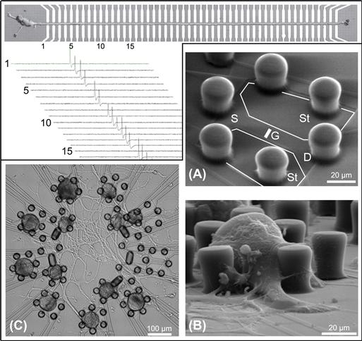
FIGURE I.2.13.10 Photolithography and Masked Deposition/Etching Used to Create Microelectronics for Interfacing with Neurons.
Upper left: a massive array of electrodes (top image) is used to record electrical signals from a single neuron (Patolsky et al., 2006). The signals are shown in the plots below the image. Lower right: polymeric posts are used to confine neurons atop underlying transistors (Zeck and Fromherz, 2001). The device is diagrammed in (A) indicating “Stimulator wings” (St) and the transistor components (S, source; D, drain; G, gate). The device is shown with a single cell in (B). An array of devices is used to interface with a neuronal network (C). Upper left is from [Patolsky, F., Timko, B. P., Yu, G., Fang, Y., Greytak, A. B., et al. (2006). Detection, stimulation, and inhibition of neuronal signals with high-density nanowire transistor arrays. Science, 313(5790), 1100–1104.]. Adapted with permission from AAAS and from the authors. Lower Right is adapted with permission from (Zeck, G., & Fromherz, P. (2001). Noninvasive neuroelectronic interfacing with synaptically connected snail neurons immo-bilized on a semiconductor chip. Proc. Natl. Acad. Sci. USA, 98(18), 10457–10462.). Copyright (2001) National Academy of Sciences, U.S.A.
Patterning with Masters
A master is a template that is used to replicate patterns, usually in a batch-type process. Rigid masters can be used directly to imprint patterns on substrates. However, the most widespread use of masters for patterning is to create a mold, typically of an elastomeric polymer, which is subsequently used to mold the patterns. Molds are usually fabricated by curing polymeric materials in the presence of the master, which embeds the features of the master into the mold. Once separated from the master, molds can be used for printing features on substrates using molecular inks that are first applied to ink the mold, and then are transferred by contact with the protruding features of the mold with a surface. Alternatively, they can be brought into contact with a surface to create channels of the void features in the mold on a substrate, which can be used for patterning by a liquid ink flowing through the channel. Patterning with masters is a relatively cheap methodology to mass-produce features over large surface areas. Also, the use of conformal molds allows patterning on curved surfaces (Jackman et al., 1995). Cylindrical molds with patterned features also offer the possibility of a direct roll-on patterning process of a planar surface (Xia et al., 2004). Typically, patterning with masters does not offer as high spatial resolution as some direct-write patterning techniques.
Imprinting with a Master
Imprinting with a master is essentially the same concept as imprinting with a stylus, as described above, except that a master is used to imprint many features at once, instead of using a stylus and serially imprinting or writing one feature at a time. The master is fabricated from a relatively hard material such that it resists deformation when it is pressed against the substrate. The master contains a rigid relief pattern that molds the substrate into the shape which it is pressed into. Imprinting with a master is used often to pattern polymer films; however, other substrates can be used with the main requirement being that substrate must be soft enough to be deformed by the master. The resolution of features obtained from imprinting with a master is dictated by the durability of the master, the physical properties of the substrate, and the mechanical pressure applied during embossing. Feature sizes as small as 10 nm are attainable by imprinting with masters (Geissler and Xia, 2004).
Printing (Use of Protruding Features of a Mold)
Printing of patterns using molds is most widely done by soft lithography, a suite of related techniques that generally refers to the use of soft, elastomeric polymer molds to create patterns on substrates. Here, liquid monomer is poured onto a rigid master and then cured; when separated from the master the polymer mold retains the topography of the original master. These topographical features are then transferred to another substrate for patterning. Masters can be created using photolithographic techniques (described above), direct-write patterning or even relatively low-tech methods such as gluing rigid objects together so that they create necessary voids in the polymer (Allen et al., 2005; Hill and Shear, 2006). The most widely used polymer in soft lithography is PDMS. PDMS has numerous advantageous qualities (Whitesides et al., 2001) that contribute to its popularity, some of which include that it is low cost, available commercially, easily prepared, flexible, optically flat (good for optical microscopy), insulating, resistant to harsh chemicals (including hydrofluoric acid, a popular glass etchant), and relatively permeable to biological gases. PDMS has tunable surface properties, and can be reversibly or irreversibly bound to surfaces such as glass, creating liquid-tight seals for controlled flows. The elasticity and adherent nature of PDMS make it an extremely versatile mold, as these properties enable the mold to remain in close conformation with curved or otherwise non-uniform surfaces, which contributes to the ability to pattern large surface areas (up to hundreds of square centimeters) (Xia and Whitesides, 1998) with a single mold.
Printing in the context of soft lithography is commonly referred to as microcontact printing (Figure I.2.13.11), and was first demonstrated by Whitesides and co-workers at Harvard University in the early 1990s (Kumar and Whitesides, 1993). In microcontact printing, an elastomeric stamp created from a rigid master is used to print molecular inks (dried) on substrates with patterned feature sizes in the micrometer to nanometer size range (Xia and Whitesides, 1998; Whitesides et al., 2001; Geissler and Xia, 2004; Ducker et al., 2008). This technology was first demonstrated with printing of alkanethiol SAMs on gold surfaces (Kumar and Whitesides, 1993), and was benefitted by the fact that alkanethiols have a high affinity to gold and form dense monolayers on gold surfaces (Love et al., 2005). Thus, when a PDMS stamp containing SAM-forming molecules contacts the gold surface, the molecules dissociate from the PDMS stamp and assemble on the surface. The feature sizes of patterns generated by microcontact printing are determined by the mechanical properties of the stamp, the deposition conditions (i.e., pressure and duration of application), and the leakiness or spreading properties of the molecular ink during the stamping process.
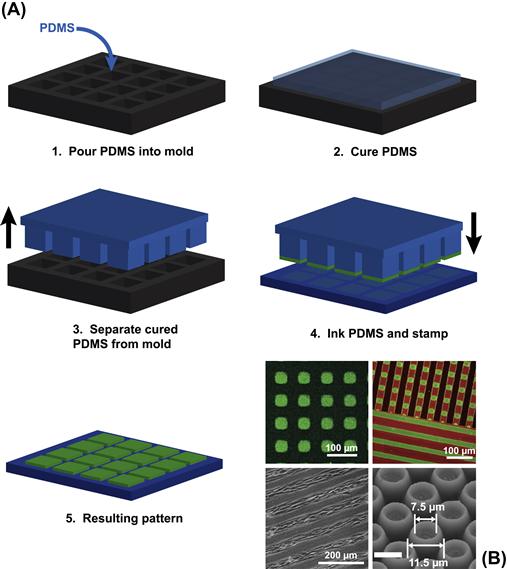
FIGURE I.2.13.11 Microcontact Printing. (A) The typical steps involved in microcontact printing. (B) Clockwise from upper left: checkered pattern of fluorescent protein formed by microcontact printing on a polymer; multicomponent polymer brush patterns formed by microcontact printing; anemone-shaped patterns of stimulus-responsive polymer patterned by microcontact printing (Chen et al., 2009); cell patterning on poly(ethylene terephthalate) by microcontact printing of a protein-resistant comb polymer and backfilling with fibronectin (Hyun et al., 2003).
Upper left is adapted with permission from (Ma H., Li, D Sheng, X., Zhao B., & Chilkoti, A. (2006b). Protein-resistant polymer coatings on silicon oxide by surface-initiated atom transfer radical polymerization. Langmuir, 22(8), 3751–3756.). Copyright (2006) American Chemical Society. Upper right is adapted with permission from (Zhou, F., Zheng, Z., Yu, B., Liu, W., & Huck, W. T. S. (2006). Multicomponent polymer brushes. J. Am. Chem. Soc., 128(50), 16253–16258.). Copyright (2006) American Chemical Society. Lower right and left are adapted with permission from Wiley–Blackwell.
Two papers from the Whitesides group from the 1990s stand out as being particularly relevant to the field of biomaterials. The first by Lopez et al. (1993) demonstrated the power of surface engineering to spatially control the adhesion of cells in adherent cultures. Although the patterns in this study were not fabricated using soft lithography, but were instead created in a direct-write process, many of the conceptual ideas in this paper reappeared in subsequent papers from the Whitesides group and others that used soft lithography to pattern alkanethiols on surfaces. A second seminal paper, by Singhvi et al. (1994), followed from this study and was one of the earliest works demonstrating the important role that geometrical patterns on a surface could play in confining cell shape, and hence their function and/or behavior. This work revealed the power of micropatterning on the length scale of the cell.
Since the initial demonstration of the printing of SAMs, other researchers have extended the use of soft lithography to include patterning of polymers (James et al., 1998; Zhou et al., 2006; Chen et al., 2009), proteins (including functional antibodies and enzymes) (Bernard et al., 1998, 2000, 2001a; Kung et al., 2000; Renault et al., 2002; Tan et al., 2002; Ma et al., 2006b), and cells (Hyun et al., 2003) on various surfaces, including glass, silicon, and metals. In one example of diversifying beyond printing alkanethiol SAMs on gold, Chilkoti and co-workers showed that a class of random oligoethylene glycol-functionalized methacrylate terpolymers that are protein resistant could be spin-coated on to a micropatterned PDMS stamp (Ma et al., 2005). Bringing the stamp into contact with a substrate resulted in transfer of the polymer only in regions of the stamp that were in contact with surface. This selective delamination process worked with a surprisingly large number of materials, and provided a simple method to stamp protein-resistant polymer features with controlled lateral dimensions and height (controlled by the thickness of the polymer layer spin-coated on to the stamp) on a surface.
Use of Void Features of a Mold
While printing makes use of the protruding features of a mold, a complementary set of patterning techniques utilize the void features in the mold (Xia et al., 1996a, 1997). When a mold with a striped pattern is affixed to a substrate, the voids in the mold form channels that can be filled with liquid to create patterns. In microfluidic patterning, a network of channels is used to deliver liquids to specific locations on a substrate. Here, liquids can be used to deliver reagents locally to microdevices on microfluidic chips (Figure I.2.13.12, right) (Juncker et al., 2002; Taylor et al., 2005), to deposit biomolecules onto the surface through adsorption or attachment chemistries (Bernard et al., 2001b; Dertinger et al., 2002; Fosser and Nuzzo, 2003), to locally dissolve parts of the underlying substrate (Rodriguez et al., 2003) or to serve as a mask for photolithography (Figure I.2.13.12, left) (Chen et al., 2003). See McDonald et al. (2000) for a good review of microfluidic systems.
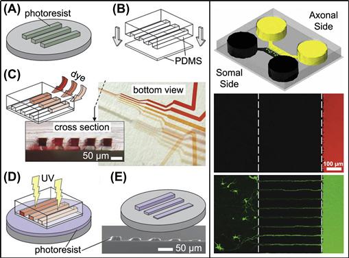
FIGURE I.2.13.12 Microfluidics. Left: microfluidic channels containing fluids of varying opacity are used as a mask for photolithography (Chen et al., 2003). Flow channels are created using an elastomertic mold (B) developed from a master pattern (A). The channels are filled with fluids of varying opacity (C), which modulates the light exposure to the underlying photoresist (D) and hence creates patterns that vary in height (E). Right: a microfluidic cell culture platform (top) is used to isolate axons of neurons, which can be targeted with effectors located in either of the fluid chambers (Taylor et al., 2005). Fluidic isolation of a dye on the axonal side of the chamber is shown in the middle panel. The bottom panel shows neurons that became stained with a dye that is located in the axonal side of the chamber.
Left is adapted with permission from (Chen, C., Hirdes, D., & Folch, A. (2003). Gray-scale photolithography using microfluidic photomasks. Proc. Natl. Acad. Sci., 100(4), 1499–1504.). Copyright (2003) National Academy of Sciences, U.S.A. Right is adapted with permission from Nature Publishing Group.
Channels in a mold can also be used to deliver a polymer solution to a surface in a spatially delimited manner, which are then hardened or cured (Kim et al., 1995). Subsequent removal of the elastomeric mold leaves behind deposits of cured polymer in the regions of the surface in contact with the channels of the original mold. Several variants of this type of patterning have been developed, such as capillary force lithography (CFL) (Suh et al., 2005; Liu et al., 2006), micromolding in capillaries (MIMIC) (Xia et al., 1996b; Beh et al., 1999), and solvent-assisted micromolding (SAMIM) (Kim et al., 1997).
Patterning by Self-Assembly of Polymers and Colloids
Patterning by self-assembly of polymers and colloids is a powerful technique because, when properly executed, it requires minimal effort to produce the patterns. Self-assembled patterns are created by using experimental conditions where intermolecular or inter-particle forces cause polymers or colloidal particles to phase separate or aggregate in a spatially defined pattern driven by minimization of the free energy of the system. Self-assembled patterning can be used to pattern large surface areas with features ranging in resolution from the nanoscale to the microscale. Three examples of patterning by self-assembly are highlighted in this section: block copolymer self-assembly; nanosphere lithography; and magnetic self-assembly (Figure I.2.13.13).
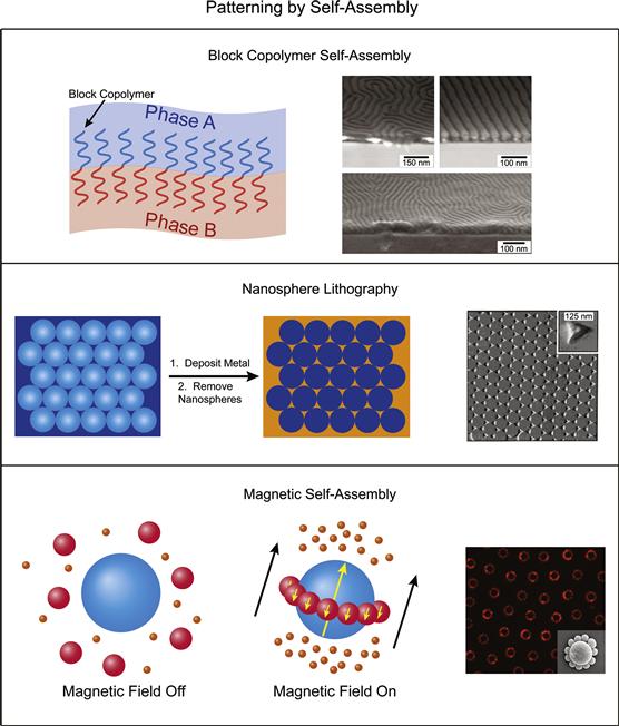
FIGURE I.2.13.13 Patterning by Self-Assembly. Top: block copolymer patterning on surfaces due to microphase separation between the polymer blocks (Ouk Kim et al., 2003). Middle: in nanosphere lithography, self-assembled, close packed nanospheres are used as a mask for creating metallic patterns on surfaces. Bottom: magnetic fields can be used to pattern magnetically susceptible objects. Here, rings of non-magnetic spheres are localized around larger paramagnetic spheres in solutions of magnetic ferrofluid (Erb et al., 2009). We note that the nature of this work was to position and align objects in three dimensions; however, this technique should be readily adaptable to surface patterning of three-dimensional objects.
Data panels on the right: Top and Bottom are adapted with permission from Nature Publishing Group. Middle is adapted with permission from (Haynes, C., & Van Duyne, R. (2001). Nanosphere lithography: A versatile nanofabrication tool for studies of size-dependent nanoparticle optics. J. Phys. Chem. B., 105(24), 5599–5611.). Copyright (2001) American Chemical Society.
Block Copolymer Self-Assembly
Block copolymer self-assembly is an example of self-assembled patterning at the molecular level. Patterning with block copolymers is accomplished by using a block copolymer that has two or more blocks that are immiscible with each other. A solution of the block copolymer is deposited on to a surface where it undergoes microphase segregation as the solvent evaporates. This segregation then leads to the formation of highly ordered surface patterns on the nanometer length scale that can readily cover large surface areas, although defects are a common problem on larger coverage areas. The nanometer-scale lateral resolution over a macroscopic surface area afforded by block copolymer self-assembly makes it a high-resolution, high-throughput patterning technique (Li and Ober, 2006). Patterns can be controlled by altering a number of variables: the sequence and length of the blocks; the degree of immiscibility of the blocks; the physico-chemical properties of the solvent; the ambient conditions during thin film deposition; film thickness; and surface chemistry (Nie and Kumacheva, 2008). As described in Nie and Kumacheva’s review (2008), patterned block copolymer films have been used as photonic crystals (Valkama et al., 2004), optical waveguides (Kim et al., 2005), and as templates for the growth of inorganic materials (Shin et al., 2002). They have also been used to create surfaces with tunable wettability (Xu et al., 2006b), and they can also be used as masks for patterning. In this approach, one phase of the block copolymer pattern is selectively removed, which leaves a nanoporous film behind that can serve as a mask (Nie and Kumacheva, 2008). For examples of block copolymer patterning, as well as reviews, see references Hamley, 2003; Park et al., 2003; Lie and Ober, 2006; Kim and Hinsberg, 2008; Nie and Kumacheva, 2008.
Nanosphere Lithography
Nanosphere lithography exploits the self-assembly of nanoscale objects to create a periodic mask or pattern. In nanosphere lithography, a solution of relatively monodisperse nanospheres – usually composed of a polymer – are delivered to a flat substrate from solution. Under specific conditions, the nanospheres self-assemble into a hexagonal, close-packed monolayer as the solvent evaporates, which leaves voids between the nanospheres where the underlying substrate is exposed. The nanosphere monolayer is then used as a mask to pattern the underlying substrate. Typically, nanosphere masks are used to mask the deposition of metals onto a substrate. After metal deposition, the nanospheres are removed from the surface, and leave behind metal pyramids in the regions corresponding to the void volumes between the nanospheres. For a detailed review on creating metal nanoparticles by nanosphere lithography, see Haynes and Van Duyne (2001). Template stripping has been used in combination with nanosphere lithography to create ultra-flat metal triangles (instead of pyramids) on surfaces using a similar deposition scheme (Frey et al., 2000). However, not all forms of nanosphere lithography involve metal deposition. For example, a metal microgrid template was used to direct dewetting of solutions on surfaces containing colloidal particles (including nanospheres and microspheres) (Celio et al., 2006). Once dewetting is complete, highly ordered patterns of the particles are formed over a large surface area on the underlying substrate.
Magnetic Self-Assembly
In magnetic self-assembly, nano-to-microscale particles with a magnetic susceptibility align or orient themselves in a magnetic field. In one implementation of this approach, magnetic nanoparticles can be directed to surfaces in a pattern, which can then serve as a mask for deposition of proteins or other biological materials (Bardea and Naaman, 2009). Magnetic particles have also been attached to cells to enable magnetism-directed cell patterning (Alsberg et al., 2006; Ino et al., 2007; Lin et al., 2008). Magnetic ferrofluid can also be used to template the self-assembly of non-magnetic materials, such as microspheres and cells (Yellen et al., 2006; Erb et al., 2009; Krebs et al., 2009). In this case, non-magnetic objects are positioned in three-dimensional space, due to the self-assembly of the magnetic medium surrounding them as the medium aligns with the external magnetic field.
Dynamic Patterning
The discussion of patterning thus far has mostly related to the formation of static patterns, which offer little control to the designer after formation, and often are subject to erosion or contamination over time. An emerging field of surface patterning is focused on the creation of dynamic or “smart” patterns. These patterns are designed to respond to external cues in the local environment. One motivation for the creation of dynamic patterns or materials is to create micro-mechanical components for use in microfluidic devices, diagnostics, theraputics or other sensing devices (Beebe et al., 2000; Jager et al., 2000; Terray et al., 2002; Alexander and Shakesheff, 2006; Dong et al., 2006; Peppas et al., 2006; Sidorenko et al., 2007; Kaehr and Shear, 2008). A motivation for dynamic patterning more relevant to the focus of this chapter, however, is to enable spatio-temporal control over interfaces used to study the cellular microenvironment, as well as those used in chip-based sensing devices. Dynamic patterning is particularly important, because most biological processes are triggered by temporal cues in the local environment. For example, intracellular signal cascades that are driven by ligand binding to receptors, clustering of receptors in membranes, and remodeling of the extracellular matrix due to mechano-chemical stimuli, are all dynamic processes in biology. Engineered dynamic interfaces present a biologically inspired – although abiological – methodology to provide temporal control of biological interactions at artificial surfaces. For example, Milan Mrksich’s group at the University of Chicago has created SAMs on gold that present ligands at the SAM–water interface that can be switched between an active or inactive state via electrochemical signals from an underlying gold electrode (Mrksich, 2002, 2009). They have used these surfaces to study the interactions between ligands and cell membranes during cell attachment to micropatterned surfaces (Yeo et al., 2003) and heterogeneous (Yousaf et al., 2001) cell patterning. Furthermore, the Chilkoti group has used elastin-like biopolymers, which actuate with a thermal or saline stimulus, to enable dynamic and reversible spatial localization of proteins to patterned templates (Frey et al., 2003a,b; Nath and Chilkoti, 2003; Hyun et al., 2004b) (Figure I.2.13.14) with application for the fabrication of rewriteable surfaces for cell studies and biosensors.
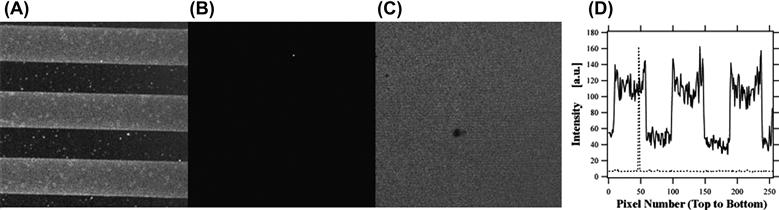
FIGURE I.2.13.14 Dynamic Patterning (Frey et al., 2003b). Shown in (A) is a confocal fluorescence image of a pattern of fluorescent antibodies localized to regions containing antigen coupled to a stimulus-responsive polymer (light regions of the image). Once triggered, the pattern is completely erased, as shown in (B) – an image using the same gain settings as in (A) – and again in (C), an image with enhanced gain settings to show uniformity of the background. (D) shows vertical intensity line plots drawn through (A) (solid line) and (B) (dashed line), which further verify complete elimination of the initial pattern shown in (A). Reprinted with permission from Wiley-Blackwell.
Three-Dimensional Patterning
Three-dimensional patterning is a new and exciting development in the field of surface patterning. A major motivation for the development of three-dimensional patterning is the fact that cells exist in a three-dimensional environment in nature. However, cell-based experimentation in laboratories typically involves cell cultures growing on planar substrates, where they interact only in two dimensions and are often irrelevant because cells exist in three dimensions in the body. The benefits of three-dimensional patterning are also relevant for the design of biosensor and diagnostics, as control of an extra dimension in device fabrication will enable the design of new sensing architectures and transduction modalities with potentially improved figure-of-merit. In addition, three-dimensional control of patterning will also yield better control over the design of microfluidic lab-on-a-chip devices.
Many of the techniques described in the preceding sections can be used for three-dimensional patterning. For example, mask-based photolithography in combination with masked deposition or etching can be used to fabricate three-dimensional structures using multiple steps to build up features in the third dimension layer-by-layer (Zeck and Fromherz, 2001). This technique works well for patterning large surface areas; however, the processing involved can be quite laborious and time-consuming, as each layer requires a standalone photolithographic process. Three-dimensional features can also be deposited from voids in elastomeric molds, as discussed in the section on soft lithography. In addition, soft lithography (Hammond and Whitesides, 1995; Clark et al., 1997; Clark and Hammond, 1998; Jiang and Hammond, 2000) and scanning probe techniques (Lee et al., 2009) can be used to confine precursors in two dimensions on a substrate that can initiate self-assembly of features in a third dimension via molecularly thin, layer-by-layer (LBL) deposition of oppositely charged polyelectrolytes. This approach provides nanometer spatial resolution in the third dimension; however, assembly of polyelectrolyte layers via LBL deposition can be time-consuming when substantial feature heights are desired.
Another direct-write example of three-dimensional patterning is photothermal needle etching, in which an agarose gel is photothermally ablated by scanning a needle, with a laser that is continually focused on it, throughout the gel (Moriguchi and Yasuda, 2006). In a final example of three-dimensional patterning, robotic inkjet printing of viscoelastic polymers on surfaces has been used to create very complex three-dimensional architectures in a direct-write manner (Gratson et al., 2004), and some of these patterned three-dimensional structures have been used in tissue engineering (Woodfield et al., 2004), and for microfluidic (Therriault et al., 2003) applications. This technique suffers the drawbacks of any direct-write method, in that it is laborious to pattern large surface areas via serial scanning. However, inkjet printing has the attractive features that the spatial resolution is in range of the hundreds of nanometers, and complete three-dimensional control is possible as arbitrary features that can be fabricated by this methodology.
The rest of this section will detail some other techniques for three-dimensional patterning that use a different set of principles than those described so far.
Multiphoton Lithography
Multiphoton lithography (MPL) is a laser-based, direct-write approach to three-dimensional patterning in which multiphoton excitation of photoinitiators or photosensitizers is used to photocross-link or photopolymerize materials at the focus of a high instantaneous-energy, pulsed laser beam. As multiphoton excitation varies nonlinearly with the intensity of the excitation source, these photochemical reactions are confined to a small volume, or voxel, within the laser focus where intensity is large enough to excite a photochemical process of interest. This voxel can be translated in three dimensions within a solution of photoactive materials to locally cure photoactive material from solution. The remaining uncured solution can be rinsed away, leaving behind hardened, freestanding three-dimensional features. The resolution limit of this technique is ~250 nm, and can be scaled to the microscale; however, fabrication of larger features usually requires higher laser power, which can be a limiting factor in some applications. The use of a motorized mechanical stage allows automated patterning in the X–Y dimensions, while auto-focusing mechanisms can provide automated control over the Z dimension.
MPL has been widely used to create three-dimensional features from UV-curable synthetic resins. Complex serial scanning algorithms have enabled the fabrication of micronscale replicas of livestock, sculptures (Serbin et al., 2003), houses (Lafratta et al., 2007), and the fabrication of three-dimensional tattoos on biological specimens (Baldacchini et al., 2004), free-standing metallized wires and other electrical microcomponents (Lafratta et al., 2007; Li and Fourkas, 2007), micro-mechanical parts (Maruo et al., 2003), and photonic crystals (Seet et al., 2006; Tetreault et al., 2006; Lafratta et al., 2007; Li and Fourkas, 2007). Perhaps more biologically relevant, however, is the use of MPL to pattern protein-based materials in three dimensions (Pitts et al., 2000, 2002; Basu and Campagnola, 2004; Basu et al., 2004, 2005; Kaehr et al., 2004, 2006; Allen et al., 2005; Hill et al., 2005; Hill and Shear, 2006; Kaehr and Shear, 2007, 2008; Lyon et al., 2007; Nielson et al., 2009; Seidlits et al., 2009). In this approach, solutions of proteins and photosensitizers are used in place of synthetic resins to create biologically compatible three-dimensional protein microstructures. Shear and co-workers have used this methodology to generate three-dimensional protein structures on-the-fly in the presence of living neurons (Kaehr et al., 2004), as well as protein-based houses for bacteria (Kaehr and Shear, 2007; Nielson et al., 2009). This work opens up the possibility of directing single cell and cell–cell interaction experiments in real time, as opposed to relying on patterning a substrate before cell seeding. They have also created three-dimensional protein–hydrogel structures for cell cultures (Seidlits et al., 2009), three-dimensional multi-enzyme reactors (Allen et al., 2005; Hill and Shear, 2006), protein-based conductive wires (Hill et al., 2005), and protein hydrogel microactuators (Kaehr and Shear, 2008). Laser scanning of masks combined with scanning in the vertical dimension was demonstrated as a mask-based, multiphoton variant of projection lithography in three dimensions (Kaehr and Shear, 2007). More recently, laser scanning of a dynamic digital micro-mirror device was used to create protein-based tissue micro-replicas of monkey skulls and insects using high-resolution X-ray computed tomography data (Nielson et al., 2009) (Figure I.2.13.15).
FIGURE I.2.13.15 Three-dimensional protein microstructures fabricated by multiphoton lithography (Neilson et al., 2009). (A) Complex protein microstructures are created by laser scanning with a digital micromirror device. (B) Houses for bacteria made from three-dimensional protein microstructures. All Scale bars, 10 µm.
Adapted with permission from Wiley-Blackwell.
Holographic Lithography
Holographic lithography is a three-dimensional patterning technique based on the projection of three-dimensional images using interference patterns from intersecting laser beams. In this method, multiple coherent lasers are aligned, such that they interfere with one another to create periodic intensity patterns in an image plane. By controlling the number of interfering beams and their relative alignment, phase, amplitude, wave vector, and polarization, one can vary the complexity of the projected images. With the appropriate number of beams and alignment (Del Campo and Greiner, 2007), three-dimensional periodic lattices can be projected on to an image plane. This projection can be used to polymerize photoresists and create three-dimensional objects from the projected images. Holographic patterning is typically used to create three-dimensional templates for fabrication of photonic crystals (Geissler and Xia, 2004; Del Campo and Greiner, 2007). A major advantage of holographic patterning over other methods of three-dimensional patterning is that, once the necessary optics are aligned and configured, it is relatively simple to generate three-dimensional patterns quickly without the use of masks or serial scanning. The drawbacks of this method, however, are the complexity of the alignment procedure, as well as the optical components and sources needed. A holographic approach that is somewhat less technically challenging and more user-friendly uses a spatial light modulator that is illuminated by a single beam and projects three-dimensional holograms from computer generated bitmap images (Jenness et al., 2008). Simultaneous generation of multiple three-dimensional polymeric and protein microstructures has been accomplished using this technique (Jenness et al., 2010).
Conclusions
Surface patterning has become an extremely important tool in biomedical research. The ability to precisely define the spatial location of biomolecules and/or cells on a surface or in three dimensions provides researchers with a powerful tool to examine the interplay between biomolecules, cells, and artificial materials in a highly controlled spatial environment. This chapter has reviewed a diverse set of patterning techniques, common concerns that need to be addressed in patterning biomolecules and cells, and important figures-of-merit of different patterning methods that should provide the reader with an intelligent stepping stone to sources in the primary literature for a deeper, in-depth investigation of this area of research. This chapter should also help the reader in making a rational decision about the choice of the patterning methodology that is suitable for a particular application. In conclusion, we hope that this chapter will serve as a beginner’s guide for those who wish to delve deeper into the field of biomolecular and cellular patterning in two and three dimensions.
Bibliography
1. Alexander C, Shakesheff K. Responsive polymers at the biology/materials science interface. Adv Mater. 2006;18(24):3321–3328.
2. Allen R, Nielson R, Wise DD, Shear JB. Catalytic three-dimensional protein architectures. Anal Chem. 2005;77(16):5089–5095.
3. Alsberg E, Feinstein E, Joy M, Prentiss M, Ingber D. Magnetically-guided self-assembly of fibrin matrices with ordered nano-scale structure for tissue engineering. Tissue Eng. 2006;12(11):3247–3256.
4. Amiji M, Park K. Surface modification of polymeric biomaterials with poly (ethylene oxide), albumin, and heparin for reduced thrombogenicity. J Biomater Sci., Polym Ed. 1993;4(3):217–234.
5. Baldacchini T, LaFratta C, Farrer RA, Teich M, Saleh B, et al. Acrylic-based resin with favorable properties for three-dimensional two-photon polymerization. J Appl Phys. 2004;95:6072.
6. Bard A, Denuault G, Lee C, Mandler D, Wipf D. Scanning electrochemical microscopy: A new technique for the characterization and modification of surfaces. Accounts Chem Res. 1990;23(11):357–363.
7. Bardea A, Naaman R. Magnetolithography: From bottom-up route to high throughput. Small. 2009;5(3):316–319.
8. Basu S, Campagnola P. Enzymatic activity of alkaline phosphatase inside protein and polymer structures fabricated via multiphoton excitation. Biomacromolecules. 2004;5(2):572–579.
9. Basu S, Wolgemuth C, Campagnola P. Measurement of normal and anomalous diffusion of dyes within protein structures fabricated via multiphoton excited cross-linking. Biomacromolecules. 2004;5(6):2347–2357.
10. Basu S, Cunningham L, Pins G, Bush K, Taboada R, et al. Multiphoton excited fabrication of collagen matrices cross-linked by a modified benzophenone dimer: Bioactivity and enzymatic degradation. Biomacromolecules. 2005;6(3):1465–1474.
11. Bearinger JP, Terrettaz S, Michel R, Tirelli N, Vogel H, et al. Chemisorbed poly(propylene sulphide)-based copolymers resist biomolecular interactions. Nat Mater. 2003;2(4):259–264.
12. Beebe D, Moore J, Bauer J, Yu Q, Liu R, et al. Functional hydrogel structures for autonomous flow control inside microfluidic channels. Nature. 2000;404(6778):588–590.
13. Beh W, Kim I, Qin D, Xia Y, Whitesides G. Formation of patterned microstructures of conducting polymers by soft lithography, and applications in microelectronic device fabrication. Adv Mater. 1999;11(12):1038–1041.
14. Bernard A, Delamarche E, Schmid H, Michel B, Bosshard H, et al. Printing patterns of proteins. Langmuir. 1998;14(9):2225–2229.
15. Bernard A, Renault J, Michel B, Bosshard H, Delamarche E. Microcontact printing of proteins. Adv Mater. 2000;12(14):1067–1070.
16. Bernard A, Fitzli D, Sonderegger P, Delamarche E, Michel B, et al. Affinity capture of proteins from solution and their dissociation by contact printing. Nat Biotechnol. 2001a;19(9):866–869.
17. Bernard A, Michel B, Delamarche E. Micromosaic immunoassays. Anal Chem. 2001b;73(1):8–12.
18. Betzig E, Trautman JK. Near-field optics: Microscopy, spectroscopy, and surface modification beyond the diffraction limit. Science. 1992;257(5067):189–195.
19. Bier FF, von Nickisch-Rosenegk M, Ehrentreich-Förster E, Reiss E, Henkel J, et al. DNA microarrays. Adv Biochem Eng Biotechnol. 2008;109:433–453.
20. Brough B, Christman K, Wong T, Kolodziej C, Forbes J, et al. Surface initiated actin polymerization from top-down manufactured nanopatterns. Soft Matter. 2007;3(5):541–546.
21. Caiazzo RJ, Maher AJ, Drummond MP, Lander CI, Tassinari OW, et al. Protein microarrays as an application for disease biomarkers. Prot Clin Appl. 2009;3(2):138–147.
22. Celio H, Barton E, Stevenson KJ. Patterned assembly of colloidal particles by confined dewetting lithography. Langmuir. 2006;22(26):11426–11435.
23. Chen C, Hirdes D, Folch A. Gray-scale photolithography using microfluidic photomasks. Proc Natl Acad Sci. 2003;100(4):1499–1504.
24. Chen T, Zhang J, Chang DP, Garcia A, Zauscher S. Fabrication of micropatterned stimulus-responsive polymer-brush “Anemone.”. Adv Mater. 2009;21(18):1825–1829.
25. Chou S. Patterned magnetic nanostructures and quantized magnetic disks. Proc IEEE. 1997;85(4):652–671.
26. Christman KL, Schopf E, Broyer RM, Li RC, Chen Y, et al. Positioning multiple proteins at the nanoscale with electron beam cross-linked functional polymers. J Am Chem Soc. 2009;131(2):521–527.
27. Clark S, Hammond PT. Engineering the microfabrication of layer-by-layer thin films. Adv Mater. 1998;10(18):1515–1519.
28. Clark S, Montague M, Hammond PT. Selective deposition in multilayer assembly: SAMs as molecular templates. Supramole Sci. 1997;4(1–2):141–146.
29. Del Campo A, Greiner C. SU-8: A photoresist for high-aspect-ratio and 3D submicron lithography. J Micromechanics and Microengineering. 2007;17(6):81–95.
30. Delehanty JB, Ligler FS. A microarray immunoassay for simultaneous detection of proteins and bacteria. Anal Chem. 2002;74(21):5681–5687.
31. Demers LM, Ginger DS, Park S-J, Li Z, Chung S-W, et al. Direct patterning of modified oligonucleotides on metals and insulators by dip-pen nanolithography. Science. 2002;296(5574):1836–1838.
32. Derby B. Bioprinting: Inkjet printing proteins and hybrid cell-containing materials and structures. J Mater Chem. 2008;18(47):5717–5721.
33. DeRisi JL, Iyer VR, Brown PO. Exploring the metabolic and genetic control of gene expression on a genomic scale. Science. 1997;278(5338):680–686.
34. Dertinger SKW, Jiang X, Li Z, Murthy VN, Whitesides GM. Gradients of substrate-bound laminin orient axonal specification of neurons. Proc Natl Acad Sci USA. 2002;99(20):12542–12547.
35. Dong L, Agarwal A, Beebe D, Jiang H. Adaptive liquid microlenses activated by stimuli-responsive hydrogels. Nature. 2006;442(7102):551–554.
36. Ducker RE, Leggett GJ. A mild etch for the fabrication of three-dimensional nanostructures in gold. J Am Chem Soc. 2006;128(2):392–393.
37. Ducker RE, Janusz S, Sun S, Leggett GJ. One-step photochemical introduction of nanopatterned protein-binding functionalities to oligo(ethylene glycol)-terminated self-assembled monolayers. J Am Chem Soc. 2007a;129(48):14842–14843.
38. Ducker RE, Montague M, Sun S, Leggett GJ. Fabrication of sub-diffraction-limit molecular structures by scanning near-field photolithography. Proc SPIE. 2007b;6645:664513.
39. Ducker RE, Garcia A, Zhang J, Chen T, Zauscher S. Polymeric and biomacromolecular brush nanostructures: Progress in synthesis, patterning and characterization. Soft Matter. 2008;4(9):1774–1786.
40. Dunn R. Near-field scanning optical microscopy. Chem Rev. 1999;99:2891–2928.
41. Eck W, Stadler V, Geyer W, Zharnikov M, Golzhauser A, et al. Generation of surface amino groups on aromatic self-assembled monolayers by low energy electron beams: A first step towards chemical lithography. Adv Mater. 2000;12(11):805–808.
42. Eigler D, Schweizer E. Positioning single atoms with a scanning tunnelling microscope. Nature. 1990;344(6266):524–526.
43. Elbert DL, Hubbell JA. Reduction of fibrous adhesion formation by a copolymer possessing an affinity for anionic surfaces. J Biomed Mat Research. 1998;42(1):55–65.
44. Erb RM, Son HS, Samanta B, Rotello VM, Yellen BB. Magnetic assembly of colloidal superstructures with multipole symmetry. Nature. 2009;457(7232):999–1002.
45. Fodor SP, Read JL, Pirrung MC, Stryer L, Lu AT, et al. Light-directed, spatially addressable parallel chemical synthesis. Science. 1991;251(4995):767–773.
46. Fosser KA, Nuzzo RG. Fabrication of patterned multicomponent protein gradients and gradient arrays using microfluidic depletion. Anal Chem. 2003;75(21):5775–5782.
47. Frey W, Woods C, Chilkoti A. Ultraflat nanosphere lithography: A new method to fabricate flat nanostructures. Adv Mater. 2000;12(20):1515–1519.
48. Frey W, Meyer D, Chilkoti A. Thermodynamically reversible addressing of a stimuli responsive fusion protein onto a patterned surface template. Langmuir. 2003a;19(5):1641–1653.
49. Frey W, Meyer D, Chilkoti A. Dynamic addressing of a surface pattern by a stimuli-responsive fusion protein. Adv Mater. 2003b;15(3):248–251.
50. Geissler M, Xia Y. Patterning: Principles and some new developments. Adv Mater. 2004;16(15):1249–1269.
51. Golzhauser A, Eck W, Geyer W, Stadler V, Weimann T, et al. Chemical nanolithography with electron beams. Adv Mater. 2001;13(11):803–806.
52. Gratson GM, Xu M, Lewis JA. Microperiodic structures: Direct writing of three-dimensional webs. Nature. 2004;428(6981):386.
53. Gross GW, Schwalm FU. A closed flow chamber for long-term multichannel recording and optical monitoring. J Neurosci Methods. 1994;52:73–85.
54. Gross GW, Wen WY, Lin JW. Transparent indium-tin oxide electrode patterns for extracellular, multisite recording in neuronal cultures. J Neurosci Methods. 1985;15(3):243–252.
55. Hamley I. Nanostructure fabrication using block copolymers. Nanotechnology. 2003;14 39–39.
56. Hammond PT, Whitesides G. Formation of polymer microstructures by selective deposition of polyion multilayers using patterned self-assembled monolayers as a template. Macromolecules. 1995;28(22):7569–7571.
57. Haynes C, Van Duyne R. Nanosphere lithography: A versatile nanofabrication tool for studies of size-dependent nanoparticle optics. J Phys Chem B. 2001;105(24):5599–5611.
58. Healy KE, Lom B, Hockberger PE. Spatial distribution of mammalian cells dictated by material surface chemistry. Biotechnol Bioeng. 1994;43(8):792–800.
59. Herrwerth S, Eck W, Reinhardt S, Grunze M. Factors that determine the protein resistance of oligoether self-assembled monolayers: Internal hydrophilicity, terminal hydrophilicity, and lateral packing density. J Am Chem Soc. 2003;125(31):9359–9366.
60. Hill RT, Shear JB. Enzyme-nanoparticle functionalization of three-dimensional protein scaffolds. Anal Chem. 2006;78(19):7022–7026.
61. Hill RT, Lyon J, Allen R, Stevenson K, Shear JB. Microfabrication of three-dimensional bioelectronic architectures. J Am Chem Soc. 2005;127(30):10707–10711.
62. Holden MA, Jung S-Y, Cremer PS. Patterning enzymes inside microfluidic channels via photoattachment chemistry. Anal Chem. 2004;76(7):1838–1843.
63. Hong S, Zhu J, Mirkin C. Multiple ink nanolithography: Toward a multiple-pen nano-plotter. Science. 1999;286(5439):523–525.
64. Hu Y, Das A, Hecht MH, Scoles G. Nanografting de novo proteins onto gold surfaces. Langmuir. 2005;21(20):9103–9109.
65. Huang N, Michel R, Voros J, Textor M, Hofer R, et al. Poly (L-lysine)-g-poly (ethylene glycol) layers on metal oxide surfaces: Surface-analytical characterization and resistance to serum and fibrinogen adsorption. Langmuir. 2001;17(2):489–498.
66. Hucknall A, Simnick A, Hill RT, Chilkoti A, Garcia A, et al. Versatile synthesis and micropatterning of nonfouling polymer brushes on the wafer scale. Biointerphases. 2009a;4(2):FA50–FA57.
67. Hucknall A, Rangarajan S, Chilkoti A. In pursuit of zero: Polymer brushes that resist the adsorption of proteins. Adv Mater. 2009b;21(23):2441–2446.
68. Hucknall A, Kim D-H, Rangarajan S, Hill RT, Reichert WM, et al. Simple fabrication of antibody microarrays on nonfouling polymer brushes with femtomolar sensitivity for protein analytes in serum and blood. Adv Mater. 2009c;21(19):1968–1971.
69. Hyun J, Zhu Y, Liebmann-Vinson A, Beebe Jr T, Chilkoti A. Microstamping on an activated polymer surface: Patterning biotin and streptavidin onto common polymeric biomaterials. Langmuir. 2001;17(20):6358–6367.
70. Hyun J, Ma H, Zhang Z, Beebe Jr TP, Chilkoti A. Universal route to cell micropatterning using an amphiphilic comb polymer. Adv Mater. 2003;15(78):576–579.
71. Hyun J, Kim J, Craig SL, Chilkoti A. Enzymatic nanolithography of a self-assembled oligonucleotide monolayer on gold. J Am Chem Soc. 2004a;126(15):4770–4771.
72. Hyun J, Lee W-K, Nath N, Chilkoti A, Zauscher S. Capture and release of proteins on the nanoscale by stimuli-responsive elastin-like polypeptide “switches.”. J Am Chem Soc. 2004b;126(23):7330–7335.
73. Ino K, Ito A, Honda H. Cell patterning using magnetite nanoparticles and magnetic force. Biotechnol Bioeng. 2007;97(5):1309–1317.
74. Jackman RJ, Wilbur JL, Whitesides GM. Fabrication of submicrometer features on curved substrates by microcontact printing. Science. 1995;269(5224):664–666.
75. Jager E, Smela E, Inganas O. Microfabricating conjugated polymer actuators. Science. 2000;290(5496):1540.
76. James C, Davis R, Kam L, Craighead H, Isaacson M, et al. Patterned protein layers on solid substrates by thin stamp microcontact printing. Langmuir. 1998;14(4):741–744.
77. Jenness NJ, Wulff KD, Johannes MS, Padgett MJ, Cole DG, et al. Three-dimensional parallel holographic micropatterning using a spatial light modulator. Opt Express. 2008;16(20):15942–15948.
78. Jenness NJ, Hill RT, Hucknall A, Chilkoti A, Clark RL. A versatile diffractive maskless lithography for single-shot and serial microfabrication. Opt Express. 2010;18(11):11754–11762.
79. Jiang X, Hammond PT. Selective deposition in layer-by-layer assembly: Functional graft copolymers as molecular templates. Langmuir. 2000;16(22):8501–8509.
80. Joglekar A, Liu H, Spooner G, Meyhöfer E, Mourou G, et al. A study of the deterministic character of optical damage by femtosecond laser pulses and applications to nanomachining. Appl Phys B: Lasers Opt. 2003;77(1):25–30.
81. Juncker D, Schmid H, Drechsler U, Wolf H, Wolf M, et al. Autonomous microfluidic capillary system. Anal Chem. 2002;74(24):6139–6144.
82. Kaehr B, Shear JB. Mask-directed multiphoton lithography. J Am Chem Soc. 2007;129(7):1904–1905.
83. Kaehr B, Shear JB. Multiphoton fabrication of chemically responsive protein hydrogels for microactuation. Proc Natl Acad Sci USA. 2008;105(26):8850–8854.
84. Kaehr B, Allen R, Javier DJ, Currie J, Shear JB. Guiding neuronal development with in situ microfabrication. Proc Natl Acad Sci USA. 2004;101(46):16104–16108.
85. Kaehr B, Ertas N, Nielson R, Allen R, Hill RT, et al. Direct-write fabrication of functional protein matrixes using a low-cost Q-switched laser. Anal Chem. 2006;78(9):3198–3202.
86. Kenausis G, Voros J, Elbert D, Huang N, Hofer R, et al. Poly (l-lysine)-g-poly (ethylene glycol) layers on metal oxide surfaces: Attachment mechanism and effects of polymer architecture on resistance to protein adsorption. J Phys Chem B. 2000;104(14):3298–3309.
87. Kenseth J, Harnisch J, Jones V, Porter M. Investigation of approaches for the fabrication of protein patterns by scanning probe lithography. Langmuir. 2001;17(13):4105–4112.
88. Kim DH, Lau KH A, Robertson JW F, Lee O-J, Jeong U, et al. Thin films of block copolymers as planar optical waveguides. Adv Mater. 2005;17(20):2442–2445.
89. Kim E, Xia Y, Whitesides G. Polymer microstructures formed by moulding in capillaries. Nature. 1995;376(17):581–584.
90. Kim E, Xia Y, Zhao X, Whitesides G. Solvent-assisted microcontact molding: A convenient method for fabricating three-dimensional structures on surfaces of polymers. Adv Mater – Including CVD – Chemical Vapor Deposition. 1997;9(8):651–653.
91. Kim H, Hinsberg W. Surface patterns from block copolymer self-assembly. J Vac Sci & Technol A: Vacuum, Surfaces, and Films. 2008;26:1369.
92. Kojima K, Moriguchi H, Hattori A, Kaneko T, Yasuda K. Two-dimensional network formation of cardiac myocytes in agar microculture chip with 1480 nm infrared laser photo-thermal etching. Lab on a Chip. 2003;3(4):292–296.
93. Krämer S, Fuierer RR, Gorman CB. Scanning probe lithography using self-assembled monolayers. Chem Rev. 2003;103(11):4367–4418.
94. Krebs MD, Erb RM, Yellen BB, Samanta B, Bajaj A, et al. Formation of ordered cellular structures in suspension via label-free negative magnetophoresis. Nano Lett. 2009;9(5):1812–1817.
95. Kumar A, Whitesides G. Features of gold having micrometer to centimeter dimensions can be formed through a combination of stamping with an elastomeric stamp and an alkanethiol “ink” followed by chemical etching. Appl Phys Lett. 1993;63:2002.
96. Kung L, Kam L, Hovis J, Boxer S. Patterning hybrid surfaces of proteins and supported lipid bilayers. Langmuir. 2000;16(17):6773–6776.
97. Lafratta CN, Fourkas JT, Baldacchini T, Farrer RA. Multiphoton fabrication. Angew Chem Int Ed. 2007;46(33):6238–6258.
98. Lee G, Shin Y-H, Son JY. Formation of self-assembled polyelectrolyte multilayer nanodots by scanning probe microscopy. J Am Chem Soc. 2009;131(5):1634–1635.
99. Lee JH, Kopecek J, Andrade JD. Protein-resistant surfaces prepared by PEO-containing block copolymer surfactants. J Biomed Mat Research. 1989;23(3):351–368.
100. Lee K-B, Park S-J, Mirkin CA, Smith JC, Mrksich M. Protein nanoarrays generated by dip-pen nanolithography. Science. 2002;295(5560):1702–1705.
101. Lee SW, Oh B-K, Sanedrin RG, Salaita K, Fujigaya T, et al. Biologically active protein nanoarrays generated using parallel dip-pen nanolithography. Adv Mater. 2006a;18(9):1133–1136.
102. Lee W-K, Caster KC, Kim J, Zauscher S. Nanopatterned polymer brushes by combining AFM anodization lithography with ring-opening metathesis polymerization in the liquid and vapor phase. Small. 2006b;2(7):848–853.
103. Levskaya A, Chevalier AA, Tabor JJ, Simpson ZB, Lavery LA, et al. Synthetic biology: Engineering Escherichia coli to see light. Nature. 2005;438(7067):441–442.
104. Li L, Fourkas JT. Multiphoton polymerization. Mater Today. 2007;10(6):30–37.
105. Li M, Ober C. Block copolymer patterns and templates. Mater Today. 2006;9(9):30–39.
106. Lin R-Z, Chu W-C, Chiang C-C, Lai C-H, Chang H-Y. Magnetic reconstruction of three-dimensional tissues from multicellular spheroids. Tissue Eng Part C: Methods. 2008;14(3):197–205.
107. Liu G, Xu S, Qian Y. Nanofabrication of self-assembled monolayers using scanning probe lithography. Acc Chem Res. 2000;33(7):457–466.
108. Liu M, Amro N, Chow C, Liu G. Production of nanostructures of DNA on surfaces. Nano Lett. 2002;2(8):863–867.
109. Liu V, Jastromb W, Bhatia S. Engineering protein and cell adhesivity using PEO-terminated triblock polymers. J Biomed Mat Research. 2002;60(1):126–134.
110. Liu Y, Klep V, Luzinov I. To patterned binary polymer brushes via capillary force lithography and surface-initiated polymerization. J Am Chem Soc. 2006;128(25):8106–8107.
111. Llanos G, Sefton M. Review: Does polyethylene oxide possess a low thrombogenicity?. J Biomat Sci., Polymer Edition. 1993;4(3):381–400.
112. Lom B, Healy KE, Hockberger P. A versatile technique for patterning biomolecules onto glass coverslips. J Neurosci Methods. 1993;50(3):385–397.
113. Lopez G, Albers M, Schreiber S, Carroll R, Peralta E, et al. Convenient methods for patterning the adhesion of mammalian cells to surfaces using self-assembled monolayers of alkanethiolates on gold. J Am Chem Soc. 1993;115(13):5877–5878.
114. López GP, Ratner BD, Tidwell CD, Haycox CL, Rapoza RJ, et al. Glow discharge plasma deposition of tetraethylene glycol dimethyl ether for fouling-resistant biomaterial surfaces. J Biomed Mater Res. 1992;26(4):415–439.
115. Love JC, Estroff L, Kriebel J, Nuzzo R, Whitesides GM. Self-assembled monolayers of thiolates on metals as a form of nanotechnology. Chem Rev. 2005;105(4):1103–1169.
116. Lyon JL, Hill RT, Shear JB, Stevenson KJ. Direct electrochemical and spectroscopic assessment of heme integrity in multiphoton photo-cross-linked cytochrome C structures. Anal Chem. 2007;79(6):2303–2311.
117. Ma H, Hyun J, Stiller P, Chilkoti A. “Non-fouling” oligo(ethylene glycol)- functionalized polymer brushes synthesized by surface-initiated atom transfer radical polymerization. Adv Mater. 2004;16(4):338–341.
118. Ma H, Hyun J, Zhang Z, Beebe Jr T, Chilkoti A. Fabrication of biofunctionalized quasi-three-dimensional microstructures of a nonfouling comb polymer using soft lithography. Adv Funct Mats. 2005;15(4):529–540.
119. Ma H, Wells M, Beebe TP, Chilkoti A. Surface-initiated atom transfer radical polymerization of oligo(ethylene glycol) methyl methacrylate from a mixed self-assembled monolayer on gold. Adv Funct Mater. 2006a;16(5):640–648.
120. Ma H, Li D, Sheng X, Zhao B, Chilkoti A. Protein-resistant polymer coatings on silicon oxide by surface-initiated atom transfer radical polymerization. Langmuir. 2006b;22(8):3751–3756.
121. MacBeath G, Schreiber SL. Printing proteins as microarrays for high-throughput function determination. Science. 2000;289(5485):1760–1763.
122. Manoharan H, Lutz C, Eigler D. Quantum mirages formed by coherent projection of electronic structure. Nature. 2000;403(6769):512–515.
123. Marshall A, Hodgson J. DNA chips: An array of possibilities. Nat Biotechnol. 1998;16(1):27–31.
124. Maruo S, Ikuta K, Korogi H. Force-controllable, optically driven micromachines fabricated by single-step two-photon microstereolithography. J Microelectromechanical Sys. 2003;12(5):533–539.
125. McDonald J, Duffy D, Anderson J, Chiu D, Wu H, et al. Fabrication of microfluidic systems in poly (dimethylsiloxane). Electrophoresis. 2000;21(1):27–40.
126. Mendes PM, Yeung CL, Preece JA. Bio-nanopatterning of surfaces. Nanoscale Res Lett. 2007;2(8):373–384.
127. Moriguchi H, Yasuda K. Photothermal microneedle etching: Improved three-dimensional microfabrication method for agarose gel for topographical control of cultured cell communities. Japanese J Appl Phys. 2006;45(30):L796–L799.
128. Mrksich M. What can surface chemistry do for cell biology?. Curr Opin Chem Biol. 2002;6(6):794–797.
129. Mrksich M. Using self-assembled monolayers to model the extracellular matrix. Acta Biomater. 2009;5(3):832–841.
130. Nagaraj VJ, Eaton S, Thirstrup D, Wiktor P. Piezoelectric printing and probing of Lectin NanoProbeArrays for glycosylation analysis. Biochem Biophys Res Commun. 2008;375(4):526–530.
131. Nath N, Chilkoti A. Fabrication of a reversible protein array directly from cell lysate using a stimuli-responsive polypeptide. Anal Chem. 2003;75(4):709–715.
132. Nie Z, Kumacheva E. Patterning surfaces with functional polymers. Nat Mater. 2008;7(4):277–290.
133. Nielson R, Shear JB. Parallel chemical dosing of subcellular targets. Anal Chem. 2006;78(17):5987–5993.
134. Nielson R, Kaehr B, Shear JB. Microreplication and design of biological architectures using dynamic-mask multiphoton lithography. Small. 2009;5(1):120–125.
135. Orchekowski R, Hamelink D, Li L, Gliwa E, vanBrocklin M, et al. Antibody microarray profiling reveals individual and combined serum proteins associated with pancreatic cancer. Cancer Res. 2005;65(23):11193–11202.
136. Ouk Kim S, Solak HH, Stoykovich MP, Ferrier NJ, De Pablo JJ, et al. Epitaxial self-assembly of block copolymers on lithographically defined nanopatterned substrates. Nature. 2003;424(6947):411–414.
137. Pardo L, Wilson WC, Boland T. Characterization of patterned self-assembled monolayers and protein arrays generated by the ink-jet method. Langmuir. 2003;19(5):1462–1466.
138. Park C, Yoon J, Thomas E. Enabling nanotechnology with self assembled block copolymer patterns. Polymer. 2003;44(22):6725–6760.
139. Patolsky F, Timko BP, Yu G, Fang Y, Greytak AB, et al. Detection, stimulation, and inhibition of neuronal signals with high-density nanowire transistor arrays. Science. 2006;313(5790):1100–1104.
140. Peppas N, Hilt J, Khademhosseini A, Langer R. Hydrogels in biology and medicine: From molecular principles to bionanotechnology. Adv Mater. 2006;18(11):1345–1360.
141. Pilobello KT, Mahal LK. Deciphering the glycocode: The complexity and analytical challenge of glycomics. Curr Opin Chem Biol. 2007;11(3):300–335.
142. Pilobello KT, Krishnamoorthy L, Slawek D, Mahal LK. Development of a lectin microarray for the rapid analysis of protein glycopatterns. Chembiochem. 2005;6(6):985–989.
143. Pilobello KT, Slawek DE, Mahal LK. A ratiometric lectin microarray approach to analysis of the dynamic mammalian glycome. Proc Natl Acad Sci USA. 2007;104(28):11534–11539.
144. Piner R, Zhu J, Xu F, Hong S, Mirkin C. “Dip-pen” nanolithography. Science. 1999;283(5402):661.
145. Pitts J, Campagnola P, Epling G, Goodman S. Submicron multiphoton free-form fabrication of proteins and polymers: Studies of reaction efficiencies and applications in sustained release. Macromolecules. 2000;33(5):1514–1523.
146. Pitts J, Howell A, Taboada R, Banerjee I, Wang J, et al. New photoactivators for multiphoton excited three-dimensional submicron cross-linking of proteins: Bovine serum albumin and Type 1 collagen. Photochemistry and Photobiology. 2002;76(2):135–144.
147. Prime K, Whitesides G. Adsorption of proteins onto surfaces containing end-attached oligo (ethylene oxide): A model system using self-assembled monolayers. J Am Chem Soc. 1993;115(23):10714–10721.
148. Ray S, Britschgi M, Herbert C, Takeda-Uchimura Y, Boxer A, et al. Classification and prediction of clinical Alzheimer’s diagnosis based on plasma signaling proteins. Nat Med. 2007;13(11):1359–1362.
149. Reetz M, Winter M, Dumpich G, Lohau J, Friedrichowski S. Fabrication of metallic and bimetallic nanostructures by electron beam induced metallization of surfactant stabilized Pd and Pd/Pt clusters. J Am Chem Soc. 1997;119(19):4539–4540.
150. Renault J, Bernard A, Juncker D, Michel B, Bosshard H, et al. Fabricating microarrays of functional proteins using affinity contact printing. Angewandte Chemie (International ed. Print). 2002;41(13):2320–2323.
151. Rodriguez I, Spicar-Mihalic P, Kuyper C, Fiorini G, Chiu D. Rapid prototyping of glass microchannels. Anal Chim Acta. 2003;496(1–2):205–215.
152. Salaita K, Wang Y, Fragala J, Vega RA, Liu C, et al. Massively parallel dip-pen nanolithography with 55,000-pen two-dimensional arrays. Angew Chem Int Ed. 2006;45(43):7220–7223.
153. Schmelmer U, Paul A, Küller A, Steenackers M, Ulman A, et al. Nanostructured polymer brushes. Small. 2007;3(3):459–465.
154. Seet K, Mizeikis V, Juodkazis S, Misawa H. Three-dimensional horizontal circular spiral photonic crystals with stop gaps below 1 μm. Appl Phys Lett. 2006;88:221101.
155. Seidlits SK, Schmidt CE, Shear JB. High-resolution patterning of hydrogels in three dimensions using direct-write photofabrication for cell guidance. Adv Funct Mater. 2009;19(22):3543–3551.
156. Serbin J, Egbert A, Ostendorf A, Chichkov BN, Houbertz R, et al. Femtosecond laser-induced two-photon polymerization of inorganic organic hybrid materials for applications in photonics. Opt Lett. 2003;28(5):301–303.
157. Shiku H, Uchida I, Matsue T. Microfabrication of alkylsilanized glass substrate by electrogenerated hydroxyl radical using scanning electrochemical microscopy. Langmuir. 1997;13(26):7239–7244.
158. Shin K, Leach K, Goldbach J, Kim D, Jho J, et al. A simple route to metal nanodots and nanoporous metal films. Nano Lett. 2002;2(9):933–936.
159. Sidorenko A, Krupenkin T, Taylor A, Fratzl P, Aizenberg J. Reversible switching of hydrogel-actuated nanostructures into complex micropatterns. Science. 2007;315(5811):487.
160. Singhvi R, Kumar A, Lopez G, Stephanopoulos G, Wang D, et al. Engineering cell shape and function. Science. 1994;264(5159):696–698.
161. Steenackers M, Küller A, Ballav N, Zharnikov M, Grunze M, et al. Morphology control of structured polymer brushes. Small. 2007;3(10):1764–1773.
162. Sugio Y, Kojima K, Moriguchi H, Takahashi K, Kaneko T, et al. An agar-based on-chip neural-cell-cultivation system for stepwise control of network pattern generation during cultivation. Sensor Actuat.: B Chem. 2004;1:156–162.
163. Suh K, Choi S, Baek S, Kim T, Langer R. Observation of high-aspect-ratio nanostructures using capillary lithography. Adv Mater. 2005;17(5):560–563.
164. Sun S, Leggett GJ. Matching the resolution of electron beam lithography by scanning near-field photolithography. Nano Lett. 2004;4(8):1381–1384.
165. Sun S, Chong KSL, Leggett GJ. Nanoscale molecular patterns fabricated by using scanning near-field optical lithography. J Am Chem Soc. 2002;124(11):2414–2415.
166. Suzuki I, Sugio Y, Moriguchi H, Jimbo Y, Yasuda K. Modification of a neuronal network direction using stepwise photo-thermal etching of an agarose architecture. J Nanobiotechnology. 2004;2(1):7.
167. Tan J, Tien J, Chen C. Microcontact printing of proteins on mixed self-assembled monolayers. Langmuir. 2002;18(2):519–523.
168. Taylor AM, Blurton-Jones M, Rhee SW, Cribbs DH, Cotman CW, et al. A microfluidic culture platform for CNS axonal injury, regeneration and transport. Nat Methods. 2005;2(8):599–605.
169. Terray A, Oakey J, Marr D. Microfluidic control using colloidal devices. Science. 2002;296(5574):1841.
170. Tetreault N, von Freymann G, Deubel M, Hermatschweiler M, Pérez-Willard F, et al. New route to three-dimensional photonic bandgap materials: Silicon double inversion of polymer templates. Adv Mater. 2006;18(4):457–460.
171. Therriault D, White SR, Lewis JA. Chaotic mixing in three-dimensional microvascular networks fabricated by direct-write assembly. Nat Mater. 2003;2(4):265–271.
172. Totzeck M, Ulrich W, Göhnermeier A, Kaiser W. Semiconductor fabrication: Pushing deep ultraviolet lithography to its limits. Nat Photonics. 2007;1:629–631.
173. Valkama S, Kosonen H, Ruokolainen J, Haatainen T, Torkkeli M, et al. Self-assembled polymeric solid films with temperature-induced large and reversible photonic-bandgap switching. Nat Mater. 2004;3(12):872–876.
174. Vega RA, Maspoch D, Salaita K, Mirkin CA. Nanoarrays of single virus particles. Angew Chem Int Ed Engl. 2005;44(37):6013–6015.
175. Wadu-Mesthrige K, Xu S, Amro N, Liu G. Fabrication and imaging of nanometer-sized protein patterns. Langmuir. 1999;15(25):8580–8583.
176. Wadu-Mesthrige K, Amro NA, Garno JC, Xu S, Liu G-Y. Fabrication of nanometer-sized protein patterns using atomic force microscopy and selective immobilization. Biophys J. 2008;80(4):1891–1899.
177. Wegscheider S, Kirsch A, Mlynek J, Krausch G. Scanning near-field optical lithography. Thin Solid Films. 1995;264(2):264–267.
178. Whitesides GM, Ostuni E, Takayama S, Jiang X, Ingber D. Soft lithography in biology and biochemistry. Ann Rev Biomed Eng. 2001;3(1):335–373.
179. Wittstock G, Schuhmann W. Formation and imaging of microscopic enzymatically active spots on an alkanethiolate-covered gold electrode by scanning electrochemical microscopy. Anal Chem. 1997;69(24):5059–5066.
180. Wittstock G, Hesse R, Schuhmann W. Patterned self-assembled alkanethiolate monolayers on gold Patterning and imaging by means of scanning electrochemical microscopy. Electroanalysis (Weinheim). 1997;9(10):746–750.
181. Woodfield TBF, Malda J, de Wijn J, Péters F, Riesle J, et al. Design of porous scaffolds for cartilage tissue engineering using a three-dimensional fiber-deposition technique. Biomaterials. 2004;25(18):4149–4161.
182. Xia N, Hu Y, Grainger D, Castner D. Functionalized poly (ethylene glycol)-grafted polysiloxane monolayers for control of protein binding. Langmuir. 2002;18(8):3255–3262.
183. Xia Y, Whitesides GM. Soft lithography. Angew Chem Int Ed. 1998;37:550–575.
184. Xia Y, Kim E, Zhao X, Rogers J, Prentiss M, et al. Complex optical surfaces formed by replica molding against elastomeric masters. Science. 1996a;273(5273):347–349.
185. Xia Y, Kim E, Whitesides G. Micromolding of polymers in capillaries: Applications in microfabrication. Chem Mater. 1996b;8(7):1558–1567.
186. Xia Y, McClelland J, Gupta R, Qin D, Zhao X, et al. Replica molding using polymeric materials: A practical step toward nanomanufacturing. Adv Mater (Weinheim). 1997;9(2):147–149.
187. Xia Y, Qin D, Whitesides G. Microcontact printing with a cylindrical rolling stamp: A practical step toward automatic manufacturing of patterns with submicrometer-sized features. Adv Mater. 2004;8(12):1015–1017.
188. Xu C, Wayland B, Fryd M, Winey K, Composto R. pH-responsive nanostructures assembled from amphiphilic block copolymers. Macromolecules. 2006b;39(18):6063–6070.
189. Xu S, Liu G. Nanometer-scale fabrication by simultaneous nanoshaving and molecular self-assembly. Langmuir. 1997;13(2):127–129.
190. Xu T, Petridou S, Lee EH, Roth EA, Vyavahare NR, et al. Construction of high-density bacterial colony arrays and patterns by the ink-jet method. Biotechnol Bioeng. 2004;85(1):29–33.
191. Xu T, Jin J, Gregory CA, Hickman JJ, Boland T. Inkjet printing of viable mammalian cells. Biomaterials. 2005;26(1):93–99.
192. Xu T, Gregory CA, Molnar P, Cui X, Jalota S, et al. Viability and electrophysiology of neural cell structures generated by the inkjet printing method. Biomaterials. 2006a;27(19):3580–3588.
193. Yang Z, Frey W, Oliver T, Chilkoti A. Light-activated affinity micropatterning of proteins on self-assembled monolayers on gold. Langmuir. 2000;16(4):1751–1758.
194. Yellen B, Erb RM, Halverson D, Hovorka O, Friedman G. Arraying nonmagnetic colloids by magnetic nanoparticle assemblers. IEEE Trans Magn. 2006;42(10):3548–3553.
195. Yeo W, Yousaf M, Mrksich M. Dynamic interfaces between cells and surfaces: Electroactive substrates that sequentially release and attach cells. J Am Chem Soc. 2003;125(49):14994–14995.
196. Yousaf MN, Houseman BT, Mrksich M. Using electroactive substrates to pattern the attachment of two different cell populations. Proc Natl Acad Sci USA. 2001;98(11):5992–5996.
197. Zauscher S, Chilkoti A. Biological applications of polymer brushes. Biointerphases. 2009;4 FA1.
198. Zeck G, Fromherz P. Noninvasive neuroelectronic interfacing with synaptically connected snail neurons immobilized on a semiconductor chip. Proc Natl Acad Sci USA. 2001;98(18):10457–10462.
199. Zhou F, Zheng Z, Yu B, Liu W, Huck WTS. Multicomponent polymer brushes. J Am Chem Soc. 2006;128(50):16253–16258.