Chapter 2
Instruction Sets
Chapter Points
• A brief review of computer architecture taxonomy and assembly language.
• Four very different architectures: ARM, PIC16F, TI C55x, and TI C64x.
2.1 Introduction
In this chapter, we begin our study of microprocessors by studying instruction sets—the programmer’s interface to the hardware. Although we hope to do as much programming as possible in high-level languages, the instruction set is the key to analyzing the performance of programs. By understanding the types of instructions that the CPU provides, we gain insight into alternative ways to implement a particular function.
We use four CPUs as examples. The ARM processor [Fur96, Jag95, Slo04] is widely used in cell phones and many other systems. (The ARM architecture comes in several versions; we will concentrate on ARM version 7.) The PIC16F is an 8-bit microprocessor designed for very efficient, low-cost implementations. The Texas Instruments C55x and C64x are two very different digital signal processors (DSPs) [Tex01, Tex02, Tex10]. The C55x has a more traditional architecture while the C64x uses very-long instruction word (VLIW) techniques to provide high-performance parallel processing.
We will start with a brief introduction to the terminology of computer architectures and instruction sets, followed by detailed descriptions of the ARM, PIC16F, C55x, and C64x instruction sets.
2.2 Preliminaries
In this section, we will look at some general concepts in computer architecture and programming, including some different styles of computer architecture and the nature of assembly language.
2.2.1 Computer Architecture Taxonomy
Before we delve into the details of microprocessor instruction sets, it is helpful to develop some basic terminology. We do so by reviewing a taxonomy of the basic ways we can organize a computer.
von Neumann architectures
A block diagram for one type of computer is shown in Figure 2.1. The computing system consists of a central processing unit (CPU) and a memory. The memory holds both data and instructions, and can be read or written when given an address. A computer whose memory holds both data and instructions is known as a von Neumann machine.
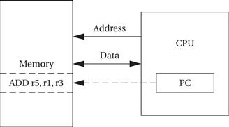
Figure 2.1 A von Neumann architecture computer.
The CPU has several internal registers that store values used internally. One of those registers is the program counter (PC), which holds the address in memory of an instruction. The CPU fetches the instruction from memory, decodes the instruction, and executes it. The program counter does not directly determine what the machine does next, but only indirectly by pointing to an instruction in memory. By changing only the instructions, we can change what the CPU does. It is this separation of the instruction memory from the CPU that distinguishes a stored-program computer from a general finite-state machine.
Harvard architectures
An alternative to the von Neumann style of organizing computers is the Harvard architecture, which is nearly as old as the von Neumann architecture. As shown in Figure 2.2, a Harvard machine has separate memories for data and program. The program counter points to program memory, not data memory. As a result, it is harder to write self-modifying programs (programs that write data values, then use those values as instructions) on Harvard machines.
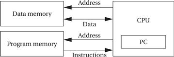
Figure 2.2 A Harvard architecture.
Harvard architectures are widely used today for one very simple reason—the separation of program and data memories provides higher performance for digital signal processing. Processing signals in real time places great strains on the data access system in two ways: First, large amounts of data flow through the CPU; and second, that data must be processed at precise intervals, not just when the CPU gets around to it. Data sets that arrive continuously and periodically are called streaming data. Having two memories with separate ports provides higher memory bandwidth; not making data and memory compete for the same port also makes it easier to move the data at the proper times. DSPs constitute a large fraction of all microprocessors sold today, and most of them are Harvard architectures. A single example shows the importance of DSP: Most of the telephone calls in the world go through at least two DSPs, one at each end of the phone call.
RISC vs. CISC
Another axis along which we can organize computer architectures relates to their instructions and how they are executed. Many early computer architectures were what is known today as complex instruction set computers (CISC). These machines provided a variety of instructions that may perform very complex tasks, such as string searching; they also generally used a number of different instruction formats of varying lengths. One of the advances in the development of high-performance microprocessors was the concept of reduced instruction set computers (RISC). These computers tended to provide somewhat fewer and simpler instructions. RISC machines generally use load/store instruction sets—operations cannot be performed directly on memory locations, only on registers. The instructions were also chosen so that they could be efficiently executed in pipelined processors. Early RISC designs substantially outperformed CISC designs of the period. As it turns out, we can use RISC techniques to efficiently execute at least a common subset of CISC instruction sets, so the performance gap between RISC-like and CISC-like instruction sets has narrowed somewhat.
Instruction set characteristics
Beyond the basic RISC/CISC characterization, we can classify computers by several characteristics of their instruction sets. The instruction set of the computer defines the interface between software modules and the underlying hardware; the instructions define what the hardware will do under certain circumstances. Instructions can have a variety of characteristics, including:
Word length
We often characterize architectures by their word length: 4-bit, 8-bit, 16-bit, 32-bit, and so on. In some cases, the length of a data word, an instruction, and an address are the same. Particularly for computers designed to operate on smaller words, instructions and addresses may be longer than the basic data word.
Little-endian vs. big-endian
One subtle but important characterization of architectures is the way they number bits, bytes, and words. Cohen [Coh81] introduced the terms little-endian mode (with the lowest-order byte residing in the low-order bits of the word) and big-endian mode (the lowest-order byte stored in the highest bits of the word).
Instruction execution
We can also characterize processors by their instruction execution, a separate concern from the instruction set. A single-issue processor executes one instruction at a time. Although it may have several instructions at different stages of execution, only one can be at any particular stage of execution. Several other types of processors allow multiple-issue instruction. A superscalar processor uses specialized logic to identify at run time instructions that can be executed simultaneously. A VLIW processor relies on the compiler to determine what combinations of instructions can be legally executed together. Superscalar processors often use too much energy and are too expensive for widespread use in embedded systems. VLIW processors are often used in high-performance embedded computing.
The set of registers available for use by programs is called the programming model, also known as the programmer model. (The CPU has many other registers that are used for internal operations and are unavailable to programmers.)
Architectures and implementations
There may be several different implementations of an architecture. In fact, the architecture definition serves to define those characteristics that must be true of all implementations and what may vary from implementation to implementation. Different CPUs may offer different clock speeds, different cache configurations, changes to the bus or interrupt lines, and many other changes that can make one model of CPU more attractive than another for any given application.
CPUs and systems
The CPU is only part of a complete computer system. In addition to the memory, we also need I/O devices to build a useful system. We can build a computer from several different chips but many useful computer systems come on a single chip. A microcontroller is one form of a single-chip computer that includes a processor, memory, and I/O devices. The term microcontroller is usually used to refer to a computer system chip with a relatively small CPU and one that includes some read-only memory for program storage. A system-on-chip generally refers to a larger processor that includes on-chip RAM that is usually supplemented by an off-chip memory.
2.2.2 Assembly Languages
Figure 2.3 shows a fragment of ARM assembly code to remind us of the basic features of assembly languages. Assembly languages usually share the same basic features:
• one instruction appears per line;
• labels, which give names to memory locations, start in the first column;
• instructions must start in the second column or after to distinguish them from labels;
• comments run from some designated comment character (; in the case of ARM) to the end of the line.
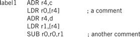
Figure 2.3 An example of ARM assembly language.
Assembly language follows this relatively structured form to make it easy for the assembler to parse the program and to consider most aspects of the program line by line. (It should be remembered that early assemblers were written in assembly language to fit in a very small amount of memory. Those early restrictions have carried into modern assembly languages by tradition.) Figure 2.4 shows the format of an ARM data processing instruction such as an ADD. For the instruction
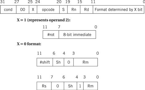
Figure 2.4 Format of an ARM data processing instruction.
ADDGT r0,r3,#5
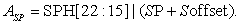
the cond field would be set according to the GT condition (1100), the opcode field would be set to the binary code for the ADD instruction (0100), the first operand register Rn would be set to 3 to represent r3, the destination register Rd would be set to 0 for r0, and the operand 2 field would be set to the immediate value of 5.
Assemblers must also provide some pseudo-ops to help programmers create complete assembly language programs. An example of a pseudo-op is one that allows data values to be loaded into memory locations. These allow constants, for example, to be set into memory. An example of a memory allocation pseudo-op for ARM is:
BIGBLOCK % 10
The ARM % pseudo-op allocates a block of memory of the size specified by the operand and initializes those locations to zero.
2.2.3 VLIW Processors
CPUs can execute programs faster if they can execute more than one instruction at a time. If the operands of one instruction depend on the results of a previous instruction, then the CPU cannot start the new instruction until the earlier instruction has finished. However, adjacent instructions may not directly depend on each other. In this case, the CPU can execute several simultaneously.
Several different techniques have been developed to parallelize execution. Desktop and laptop computers often use superscalar execution. A superscalar processor scans the program during execution to find sets of instructions that can be executed together. Digital signal processing systems are more likely to use very long instruction word (VLIW) processors. These processors rely on the compiler to identify sets of instructions that can be executed in parallel. Superscalar processors can find parallelism that VLIW processors can’t—some instructions may be independent in some situations and not others. However, superscalar processors are more expensive in both cost and energy consumption. Because it is relatively easy to extract parallelism from many DSP applications, the efficiency of VLIW processors can more easily be leveraged by digital signal processing software.
Packets
In modern terminology, a set of instructions is bundled together into a VLIW packet, which is a set of instructions that may be executed together. The execution of the next packet will not start until all the instructions in the current packet have finished executing. The compiler identifies packets by analyzing the program to determine sets of instructions that can always execute together.
Inter-instruction dependencies
To understand parallel execution, let’s first understand what constrains instructions from executing in parallel. A data dependency is a relationship between the data operated on by instructions. In the example of Figure 2.5, the first instruction writes into r0 while the second instruction reads from it. As a result, the first instruction must finish before the second instruction can perform its addition. The data dependency graph shows the order in which these operations must be performed.
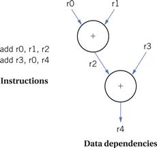
Figure 2.5 Data dependencies and order of instruction execution.
Branches can also introduce control dependencies. Consider this simple branch
bnz r3,foo
add r0,r1,r2
foo: …
The add instruction is executed only if the branch instruction that precedes it does not take its branch.
Opportunities for parallelism arise because many combinations of instructions do not introduce data or control dependencies. The natural grouping of assignments in the source code suggests some opportunities for parallelism that can also be influenced by how the object code uses registers. Consider the example of Figure 2.6. Although these instructions use common input registers, the result of one instruction does not affect the result of the other instructions.
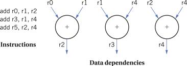
Figure 2.6 Instructions without data dependencies.
VLIW vs. superscalar
VLIW processors examine inter-instruction dependencies only within a packet of instructions. They rely on the compiler to determine the necessary dependencies and group instructions into a packet to avoid combinations of instructions that can’t be properly executed in a packet. Superscalar processors, in contrast, use hardware to analyze the instruction stream and determine dependencies that need to be obeyed.
VLIW and embedded computing
A number of different processors have implemented VLIW execution modes and these processors have been used in many embedded computing systems. Because the processor does not have to analyze data dependencies at run time, VLIW processors are smaller and consume less power than superscalar processors. VLIW is very well suited to many signal processing and multimedia applications. For example, cellular telephone base stations must perform the same processing on many parallel data streams. Channel processing is easily mapped onto VLIW processors because there are no data dependencies between the different signal channels.
2.3 ARM Processor
In this section, we concentrate on the ARM processor. ARM is actually a family of RISC architectures that have been developed over many years. ARM does not manufacture its own chips; rather, it licenses its architecture to companies who either manufacture the CPU itself or integrate the ARM processor into a larger system.
The textual description of instructions, as opposed to their binary representation, is called an assembly language. ARM instructions are written one per line, starting after the first column. Comments begin with a semicolon and continue to the end of the line. A label, which gives a name to a memory location, comes at the beginning of the line, starting in the first column:
LDR r0,[r8] ; a comment
label ADD r4,r0,r1W
2.3.1 Processor and Memory Organization
Different versions of the ARM architecture are identified by number. ARM7 is a von Neumann architecture machine, while ARM9 uses a Harvard architecture. However, this difference is invisible to the assembly language programmer except for possible performance differences.
The ARM architecture supports two basic types of data:
ARM7 allows addresses to be 32 bits long. An address refers to a byte, not a word. Therefore, the word 0 in the ARM address space is at location 0, the word 1 is at 4, the word 2 is at 8, and so on. (As a result, the PC is incremented by 4 in the absence of a branch.) The ARM processor can be configured at power-up to address the bytes in a word in either little-endian or big-endian mode, as shown in Figure 2.7.
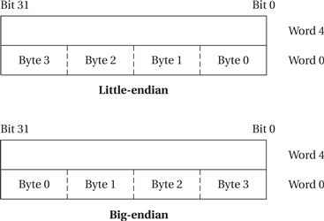
Figure 2.7 Byte organizations within an ARM word.
General-purpose computers have sophisticated instruction sets. Some of this sophistication is required simply to provide the functionality of a general computer, while other aspects of instruction sets may be provided to increase performance, reduce code size, or otherwise improve program characteristics. In this section, we concentrate on the functionality of the ARM instruction set.
2.3.2 Data Operations
Arithmetic and logical operations in C are performed in variables. Variables are implemented as memory locations. Therefore, to be able to write instructions to perform C expressions and assignments, we must consider both arithmetic and logical instructions as well as instructions for reading and writing memory.
Figure 2.8 shows a sample fragment of C code with data declarations and several assignment statements. The variables a, b, c, x, y, and z all become data locations in memory. In most cases data is kept relatively separate from instructions in the program’s memory image.
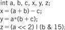
Figure 2.8 A C fragment with data operations.
ARM programming model
In the ARM processor, arithmetic and logical operations cannot be performed directly on memory locations. While some processors allow such operations to directly reference main memory, ARM is a load-store architecture—data operands must first be loaded into the CPU and then stored back to main memory to save the results. Figure 2.9 shows the registers in the basic ARM programming model. ARM has 16 general-purpose registers, r0 through r15. Except for r15, they are identical—any operation that can be done on one of them can be done on the others. The r15 register has the same capabilities as the other registers, but it is also used as the program counter. The program counter should of course not be overwritten for use in data operations. However, giving the PC the properties of a general-purpose register allows the program counter value to be used as an operand in computations, which can make certain programming tasks easier.
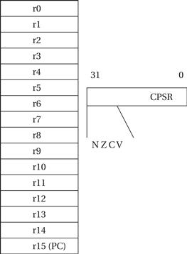
Figure 2.9 The basic ARM programming model.
The other important basic register in the programming model is the current program status register (CPSR). This register is set automatically during every arithmetic, logical, or shifting operation. The top four bits of the CPSR hold the following useful information about the results of that arithmetic/-logical operation:
• The negative (N) bit is set when the result is negative in two’s-complement arithmetic.
• The zero (Z) bit is set when every bit of the result is zero.
• The carry (C) bit is set when there is a carry out of the operation.
• The overflow (V) bit is set when an arithmetic operation results in an overflow.
These bits can be used to easily check the results of an arithmetic operation. However, if a chain of arithmetic or logical operations is performed and the intermediate states of the CPSR bits are important, they must be checked at each step because the next operation changes the CPSR values.
Example 2.1 illustrates the computation of CPSR bits.
Example 2.1 Status Bit Computation in the ARM
An ARM word is 32 bits. In C notation, a hexadecimal number starts with 0x, such as 0xffffffff, which is a two’s-complement representation of −1 in a 32-bit word.
Here are some sample calculations:
The basic form of a data instruction is simple:
ADD r0,r1,r2
This instruction sets register r0 to the sum of the values stored in r1 and r2. In addition to specifying registers as sources for operands, instructions may also provide immediate operands, which encode a constant value directly in the instruction. For example,
ADD r0,r1,#2
sets r0 to r1 + 2.
The major data operations are summarized in Figure 2.10. The arithmetic operations perform addition and subtraction; the with-carry versions include the current value of the carry bit in the computation. RSB performs a subtraction with the order of the two operands reversed, so that RSB r0,r1,r2 sets r0 to be r2 – r1. The bit-wise logical operations perform logical AND, OR, and XOR operations (the exclusive or is called EOR). The BIC instruction stands for bit clear: BIC r0,r1,r2 sets r0 to r1 and not r2. This instruction uses the second source operand as a mask: Where a bit in the mask is 1, the corresponding bit in the first source operand is cleared. The MUL instruction multiplies two values, but with some restrictions: No operand may be an immediate, and the two source operands must be different registers. The MLA instruction performs a multiply-accumulate operation, particularly useful in matrix operations and signal processing. The instruction
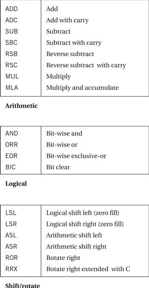
Figure 2.10 ARM data instructions.
MLA r0,r1,r2,r3
sets r0 to the value r1 × r2 + r3.
The shift operations are not separate instructions—rather, shifts can be applied to arithmetic and logical instructions. The shift modifier is always applied to the second source operand. A left shift moves bits up toward the most-significant bits, while a right shift moves bits down to the least-significant bit in the word. The LSL and LSR modifiers perform left and right logical shifts, filling the least-significant bits of the operand with zeroes. The arithmetic shift left is equivalent to an LSL, but the ASR copies the sign bit—if the sign is 0, a 0 is copied, while if the sign is 1, a 1 is copied. The rotate modifiers always rotate right, moving the bits that fall off the least-significant bit up to the most-significant bit in the word. The RRX modifier performs a 33-bit rotate, with the CPSR’s C bit being inserted above the sign bit of the word; this allows the carry bit to be included in the rotation.
The instructions in Figure 2.11 are comparison operands—they do not modify general-purpose registers but only set the values of the NZCV bits of the CPSR register. The compare instruction CMP r0, r1 computes r0 – r1, sets the status bits, and throws away the result of the subtraction. CMN uses an addition to set the status bits. TST performs a bit-wise AND on the operands, while TEQ performs an exclusive-or.
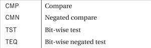
Figure 2.11 ARM compare instructions.
Figure 2.12 summarizes the ARM move instructions. The instruction MOV r0,r1 sets the value of r0 to the current value of r1. The MVN instruction complements the operand bits (one’s complement) during the move.
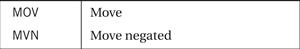
Figure 2.12 ARM move instructions.
Values are transferred between registers and memory using the load-store instructions summarized in Figure 2.13. LDRB and STRB load and store bytes rather than whole words, while LDRH and SDRH operate on half-words and LDRSH extends the sign bit on loading. An ARM address may be 32 bits long. The ARM load and store instructions do not directly refer to main memory addresses, because a 32-bit address would not fit into an instruction that included an opcode and operands. Instead, the ARM uses register-indirect addressing. In register-indirect addressing, the value stored in the register is used as the address to be fetched from memory; the result of that fetch is the desired operand value. Thus, as illustrated in Figure 2.14, if we set r1 = 0x100, the instruction
Figure 2.13 ARM load-store instructions and pseudo-operations.
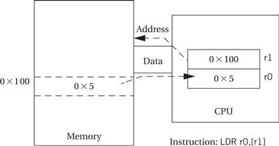
Figure 2.14 Register indirect addressing in the ARM.
LDR r0,[r1]
sets r0 to the value of memory location 0x100. Similarly, STR r0,[r1] would store the contents of r0 in the memory location whose address is given in r1. There are several possible variations:
LDR r0,[r1, – r2]
loads r0 from the address given by r1 – r2, while
LDR r0,[r1, #4]
loads r0 from the address r1 + 4.
This begs the question of how we get an address into a register—we need to be able to set a register to an arbitrary 32-bit value. In the ARM, the standard way to set a register to an address is by performing arithmetic on a register. One choice for the register to use for this operation is the program counter. By adding or subtracting to the PC a constant equal to the distance between the current instruction (i.e., the instruction that is computing the address) and the desired location, we can generate the desired address without performing a load. The ARM programming system provides an ADR pseudo-operation to simplify this step. Thus, as shown in Figure 2.15, if we give location 0x100 the name FOO, we can use the pseudo-operation
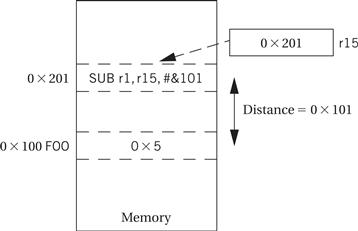
Figure 2.15 Computing an absolute address using the PC.
ADR r1,FOO
to perform the same function of loading r1 with the address 0x100. Another technique is used in high-level languages like C. As we will see when we discuss procedure calls, languages use a mechanism called a frame to pass parameters between functions. For the moment, a simplified view of the process is sufficient. A register holds a frame pointer (fp) that points to the top of the frame; elements within the frame are accessed using offsets from fp. The assembler syntax [fp,#-n] is used to take the nth location from fp.
Example 2.2 illustrates how to implement C assignments in ARM instruction.
Example 2.2 C Assignments in ARM Instructions
We will use the assignments of Figure 2.8. The semicolon (;) begins a comment after an instruction, which continues to the end of that line. The statement
x = (a + b) − c;
can be implemented by using r0 for a, r1 for b, r2 for c, and r3 for x. We also need registers for indirect addressing. In this case, we will reuse the same indirect addressing register, r4, for each variable load. The code must load the values of a, b, and c into these registers before performing the arithmetic, and it must store the value of x back to memory when it is done.
Here is code generated by the gcc compiler for this statement. It uses a frame pointer to hold the variables: a is at −24, b at −28, c at −32, and x at −36:
ldr r2, [fp, #-24]
ldr r3, [fp, #-28]
add r2, r2, r3
ldr r3, [fp, #-32]
rsb r3, r3, r2
str r3, [fp, #-36]
The operation
y = a*(b + c);
can be coded similarly, but in this case we will reuse more registers by using r0 for both a and b, r1 for c, and r2 for y. Once again, we will use r4 to store addresses for indirect addressing. The resulting code from gcc looks like this:
ldr r2, [fp, #–28]
ldr r3, [fp, #–32]
add r2, r2, r3
ldr r3, [fp, #–24]
mul r3, r2, r3
str r3, [fp, #–40]
The C statement
z = (a << 2) | (b & 15);
results in this gcc-generated code:
ldr r3, [fp, #–24]
mov r2, r3, asl #2
ldr r3, [fp, #–28]
and r3, r3, #15
orr r3, r2, r3
str r3, [fp, #–44]
More addressing modes
We have already seen three addressing modes: register, immediate, and indirect. The ARM also supports several forms of base-plus-offset addressing, which is related to indirect addressing. But rather than using a register value directly as an address, the register value is added to another value to form the address. For instance,
LDR r0,[r1,#16]
loads r0 with the value stored at location r1 + 16. Here, r1 is referred to as the base and the immediate value the offset. When the offset is an immediate, it may have any value up to 4,096; another register may also be used as the offset. This addressing mode has two other variations: auto-indexing and post-indexing. Auto-indexing updates the base register, such that
LDR r0,[r1,#16]!
first adds 16 to the value of r1, and then uses that new value as the address. The ! operator causes the base register to be updated with the computed address so that it can be used again later. Our examples of base-plus-offset and auto-indexing instructions will fetch from the same memory location, but auto-indexing will also modify the value of the base register r1. Post-indexing does not perform the offset calculation until after the fetch has been performed. Consequently,
LDR r0,[r1],#16
will load r0 with the value stored at the memory location whose address is given by r1, and then add 16 to r1 and set r1 to the new value. In this case, the post-indexed mode fetches a different value than the other two examples, but ends up with the same final value for r1 as does auto-indexing.
We have used the ADR pseudo-op to load addresses into registers to access variables because this leads to simple, easy-to-read code (at least by assembly language standards). Compilers tend to use other techniques to generate addresses, because they must deal with global variables and automatic variables.
2.3.3 Flow of Control
The B (branch) instruction is the basic mechanism in ARM for changing the flow of control. The address that is the destination of the branch is often called the branch target. Branches are PC-relative—the branch specifies the offset from the current PC value to the branch target. The offset is in words, but because the ARM is byte-addressable, the offset is multiplied by four (shifted left two bits, actually) to form a byte address. Thus, the instruction
B #100
will add 400 to the current PC value.
We often wish to branch conditionally, based on the result of a given computation. The if statement is a common example. The ARM allows any instruction, including branches, to be executed conditionally. This allows branches to be conditional, as well as data operations. Figure 2.16 summarizes the condition codes.
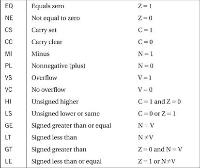
Figure 2.16 Condition codes in ARM.
We use Example 2.3 as a way to explore the uses of conditional execution.
Example 2.3 Implementing an if Statement in ARM
We will use the following if statement as an example:
if (a > b) {
x = 5;
y = c + d;
}
else x = c - d;
The implementation uses two blocks of code, one for the true case and another for the false case. Let’s look at the gcc-generated code in sections. First, here is the compiler-generated code for the a>b test:
ldr r2, [fp, #-24]
ldr r3, [fp, #-28]
cmp r2, r3
ble .L2
Here is the code for the true block:
.L2: mov r3, #5
str r3, [fp, #-40]
ldr r2, [fp, #-32]
ldr r3, [fp, #-36]
add r3, r2, r3
str r3, [fp, #-44]
b .L3
And here is the code for the false block:
ldr r3, [fp, #-32]
ldr r2, [fp, #-36]
rsb r3, r2, r3
str r3, [fp, #-40]
.L3:
The loop is a very common C statement, particularly in signal processing code. Loops can be naturally implemented using conditional branches. Because loops often operate on values stored in arrays, loops are also a good illustration of another use of the base-plus-offset addressing mode. A simple but common use of a loop is in the FIR filter, which is explained in Application Example 2.1; the loop-based implementation of the FIR filter is described in Example 2.5.
Application Example 2.1 FIR Filters
A finite impulse response (FIR) filter is a commonly used method for processing signals; we make use of it in Section 5.12. The FIR filter is a simple sum of products:
 (Eq. 2.1)
In use as a filter, the xis are assumed to be samples of data taken periodically, while the cis are coefficients. This computation is usually drawn like this:
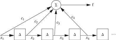
This representation assumes that the samples are coming in periodically and that the FIR filter output is computed once every time a new sample comes in. The Δ boxes represent delay elements that store the recent samples to provide the xi s. The delayed samples are individually multiplied by the ci s and then summed to provide the filter output.
Example 2.5 An FIR Filter for the ARM
Here is the C code for an FIR filter:
for (i = 0, f = 0; i < N; i++)
f = f + c[i] * x[i];
We can address the arrays c and x using base-plus-offset addressing: We will load one register with the address of the zeroth element of each array and use the register holding i as the offset.
Here is the gcc-generated code for the loop:
.LBB2:
mov r3, #0
str r3, [fp, #-24]
mov r3, #0
str r3, [fp, #-28]
.L2:
ldr r3, [fp, #-24]
cmp r3, #7
ble .L5
b .L3
.L5: ldr r3, [fp, #-24]
mvn r2, #47
mov r3, r3, asl #2
sub r0, fp, #12
add r3, r3, r0
add r1, r3, r2
ldr r3, [fp, #-24]
mvn r2, #79
mov r3, r3, asl #2
sub r0, fp, #12
add r3, r3, r0
add r3, r3, r2
ldr r2, [r1, #0]
ldr r3, [r3, #0]
mul r2, r3, r2
ldr r3, [fp, #-28]
add r3, r3, r2
str r3, [fp, #–28]
ldr r3, [fp, #–24]
add r3, r3, #1
str r3, [fp, #–24]
b .L2
.L3:
The mvn instruction moves the bitwise complement of a value.
C functions
The other important class of C statement to consider is the function. A C function returns a value (unless its return type is void); subroutine or procedure are the common names for such a construct when it does not return a value. Consider this simple use of a function in C:
x = a + b;
foo(x);
y = c − d;
A function returns to the code immediately after the function call, in this case the assignment to y. A simple branch is insufficient because we would not know where to return. To properly return, we must save the PC value when the procedure/function is called and, when the procedure is finished, set the PC to the address of the instruction just after the call to the procedure. (You don’t want to endlessly execute the procedure, after all.)
The branch-and-link instruction is used in the ARM for procedure calls. For instance,
BL foo
will perform a branch and link to the code starting at location foo (using PC-relative addressing, of course). The branch and link is much like a branch, except that before branching it stores the current PC value in r14. Thus, to return from a procedure, you simply move the value of r14 to r15:
MOV r15,r14
You should not, of course, overwrite the PC value stored in r14 during the procedure.
But this mechanism only lets us call procedures one level deep. If, for example, we call a C function within another C function, the second function call will overwrite r14, destroying the return address for the first function call. The standard procedure for allowing nested procedure calls (including recursive procedure calls) is to build a stack, as illustrated in Figure 2.17. The C code shows a series of functions that call other functions: f1() calls f2(), which in turn calls f3(). The right side of the figure shows the state of the procedure call stack during the execution of f3(). The stack contains one activation record for each active procedure. When f3() finishes, it can pop the top of the stack to get its return address, leaving the return address for f2() waiting at the top of the stack for its return.
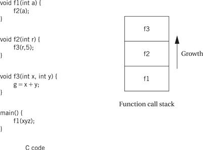
Figure 2.17 Nested function calls and stacks.
Most procedures need to pass parameters into the procedure and return values out of the procedure as well as remember their return address.
We can also use the procedure call stack to pass parameters. The conventions used to pass values into and out of procedures are known as procedure linkage. To pass parameters into a procedure, the values can be pushed onto the stack just before the procedure call. Once the procedure returns, those values must be popped off the stack by the caller, because they may hide a return address or other useful information on the stack. A procedure may also need to save register values for registers it modifies. The registers can be pushed onto the stack upon entry to the procedure and popped off the stack, restoring the previous values, before returning. Procedure stacks are typically built to grow down from high addresses.
Assembly language programmers can use any means they want to pass parameters. Compilers use standard mechanisms to ensure that any function may call any other. (If you write an assembly routine that calls a compiler-generated function, you must adhere to the compiler’s procedure call standard.) The compiler passes parameters and return variables in a block of memory known as a frame. The frame is also used to allocate local variables. The stack elements are frames. A stack pointer (sp) defines the end of the current frame, while a frame pointer (fp) defines the end of the last frame. (The fp is technically necessary only if the stack frame can be grown by the procedure during execution.) The procedure can refer to an element in the frame by addressing relative to sp. When a new procedure is called, the sp and fp are modified to push another frame onto the stack.
The ARM Procedure Call Standard (APCS) [Slo04] is a good illustration of a typical procedure linkage mechanism. Although the stack frames are in main memory, understanding how registers are used is key to understanding the mechanism, as explained below.
• r0-r3 are used to pass the first four parameters into the procedure. r0 is also used to hold the return value. If more than four parameters are required, they are put on the stack frame.
• r4-r7 hold register variables.
• r11 is the frame pointer and r13 is the stack pointer.
• r10 holds the limiting address on stack size, which is used to check for stack overflows.
Other registers have additional uses in the protocol.
Example 2.6 illustrates the implementation of C functions and procedure calls.
Example 2.6 Procedure Calls in ARM
Here is a simple example of two procedures, one of which calls another:
void f2(int x) {
int y;
y = x+1;
}
void f1(int a) {
f2(a);
}
This function has only one parameter, so x will be passed in r0. The variable y is local to the procedure so it is put into the stack. The first part of the procedure sets up registers to manipulate the stack, then the procedure body is implemented. Here is the code generated by the ARM gcc compiler for f2() with manually-created comments to explain the code:
mov ip, sp ; set up f2()’s stack access
stmfd sp!, {fp, ip, lr, pc}
sub fp, ip, #4
sub sp, sp, #8
str r0, [fp, #-16]
ldr r3, [fp, #-16] ; get x
add r3, r3, #1 ; add 1
str r3, [fp, #–20] ; assign to y
ldmea fp, {fp, sp, pc} ; return from f2()
And here is the code generated for f1():
mov ip, sp ; set up f1’s stack access
stmfd sp!, {fp, ip, lr, pc}
sub fp, ip, #4
sub sp, sp, #4
str r0, [fp, #-16] ; save the value of a passed into f1()
ldr r0, [fp, #-16] ; load value of a for the f2() call
bl f2 ; call f2()
ldmea fp, {fp, sp, pc} ; return from f1()
2.3.4 Advanced ARM Features
Several models of ARM processors provide advanced features for a variety of applications.
DSP
Several extensions provide improved digital signal processing. Multiply-accumulate (MAC) instructions can perform a 16 x 16 or 32 x 16 MAC in one clock cycle. Saturation arithmetic can be performed with no overhead. A new instruction is used for arithmetic normalization.
SIMD
Multimedia operations are supported by single-instruction multiple-data (SIMD) operations. A single register is treated as having several smaller data elements, such as bytes. The same operation is simultaneously applied to all the elements in the register.
NEON
NEON instructions go beyond the original SIMD instructions to provide a new set of registers and additional operations. The NEON unit has 32 registers, each 64 bits wide. Some operations also allow a pair of registers to be treated as a 128-bit vector. Data in a single register is treated as a vector of elements, each smaller than the original register, with the same operation being performed in parallel on each vector element. For example, a 32-bit register can be used to perform SIMD operations on 8, 16, 32, 64, or single-precision floating-point numbers.
TrustZone
TrustZone extensions provide security features. A separate monitor mode allows the processor to enter a secure world to perform operations not permitted in normal mode. A special instruction, the secure monitor call, is used to enter the secure world, as can some exceptions.
Jazelle
The Jazelle instruction set allows direct execution of 8-bit Java™ bytecodes. As a result, a bytecode interpreter does not need to be used to execute Java programs.
Cortex
The Cortex collection of processors is designed for compute-intensive applications:
• Cortex-A5 provides Jazelle execution of Java, floating-point processing, and NEON multimedia instructions.
• Cortex-A8 is a dual-issue in-order superscalar processor.
• Cortex-A9 can be used in a multiprocessor with up to four processing elements.
• Cortex-A15 MPCore is a multicore processor with up to four CPUs.
• The Cortex-R family is designed for real-time embedded computing. It provides SIMD operations for DSP, a hardware divider, and a memory protection unit for operating systems.
• The Cortex-M family is designed for microcontroller-based systems that require low cost and low-energy operation.
2.4 PICmicro Mid-Range Family
The PICmicro line includes several different families of microprocessors. We will concentrate on the mid-range family, the PIC16F family, which has an 8-bit word size and 14-bit instructions.
2.4.1 Processor and Memory Organization
The PIC16F family has a Harvard architecture with separate data and program memories. Models in this family have up to 8,192 words of instruction memory held in flash. An instruction word is 14 bits long. Data memory is byte addressable. They may have up to 368 bytes of data memory in static random-access memory (SRAM) and 256 bytes of electrically-erasable programmable read-only memory (EEPROM) data memory.
Members of the family provide several low power features: a sleep mode, the ability to select different clock oscillators to run at different speeds, and so on. They also provide security features such as code protection and component identification locations.
2.4.2 Data Operations
Address range
The PIC16F family uses a 13-bit program counter. Different members of the family provide different amounts of instruction or data memory: 2K instructions for the low-end models, 4K for medium, and 8K for large.
Instruction space
Figure 2.18 shows the organization of the instruction space. The program counter can be loaded from a stack. The lowest addresses in memory hold the interrupt vectors. The rest of memory is divided into four pages. The low-end devices have access only to page 0; the medium-range devices have access only to pages 1 and 2; high-end devices have access to all four pages.
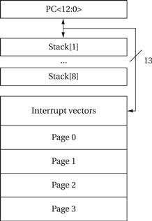
Figure 2.18 Instruction space for the PIC16F.
Data space
The PIC16F data memory is divided into four bits. Two bits of the STATUS register, RP<1:0>, select which bank is used. PIC documentation uses the term general purpose register to mean a data memory location. It also uses the term file register to refer to a location in the general-purpose register file. The lowest 32 locations of each bank contain special function registers that perform many different operations, primarily for the I/O devices. The remainder of each bank contains general-purpose registers.
Because different members of the family support different amounts of data memory, not all of the bank locations are available in all models. All models implement the special function registers in all banks. However, not all of the banks make general-purpose registers available. The low-end models provide general-purpose registers only in bank 0, the medium models banks 0 and 1, while the high-end models support general-purpose registers in all four banks.
Program counter
The 13-bit program counter is shadowed by two other registers: PCL and PCLATH. Bits PC<7:0> come from PCL and can be modified directly. Bits PC<12:8> of PC come from PCLATH which is not directly readable or writable. Writing to PCL will set the lower bits of PC to the operand value and set the high bits of PC from PCLATH.
PC stack
An 8-level stack is provided for the program counter. This stack space is in a separate address space from either the program or data memory; the stack pointer is not directly accessible. The stack is used by the subroutine CALL and RETURN/RETLW/RETFIE instructions. The stack actually operates as a circular buffer—when the stack overflows, the oldest value is overwritten.
STATUS register
STATUS is a special function register located in bank 0. It contains the status bits for the ALU, reset status, and bank select bits. A variety of instructions can affect bits in STATUS, including carry, digit carry, zero, register bank select, and indirect register bank select.
Addressing modes
PIC uses f to refer to one of the general-purpose registers in the register file. W refers to an accumulator that receives the ALU result; b refers to a bit address within a register; k refers to a literal, constant, or label.
Indirect addressing is controlled by the INDF and FSR registers. INDF is not a physical register. Any access to INDF causes an indirect load through the file select register FSR. FSR can be modified as a standard register. Reading from INDF uses the value of FSR as a pointer to the location to be accessed.
Data instructions
Figure 2.19 lists the data instructions in the PIC16F. Several different combinations of arguments are possible: ADDLW adds a literal k to the accumulator W; ADDWF adds W to the designated register f.
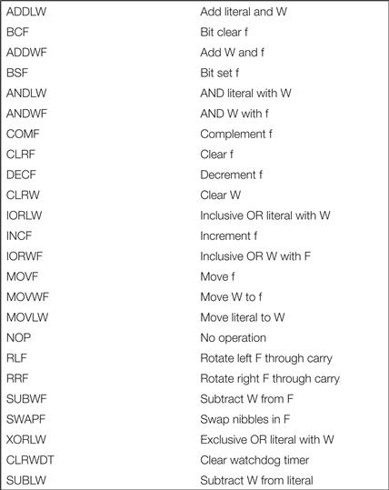
Figure 2.19 Data instructions in the PIC16F
Example 2.7 shows the code for an FIR filter on the PIC16F.
Example 2.7 FIR Filter on the PIC16F
Here is code generated for our FIR filter by the PIC MPLAB C32 compiler, along with some manually generated comments. As with the ARM, the PIC16F uses a stack frame to organize variables:
.L2:
lw $2,0($fp)
slt $2,$2,8
beq $2,$0,.L3 ; loop test---done?
nop ; fall through conditional branch here
lw $2,0($fp)
sll $2,$2,2 ; compute address of first array value
addu $3,$2,$fp
lw $2,0($fp)
sll $2,$2,2 ; compute address of second array value
addu $2,$2,$fp
lw $3,8($3) ; get first array value
lw $2,40($2) ; get second array value
mul $3,$3,$2 ; multiply
lw $2,4($fp)
addu $2,$2,$3 ; add to running sum
sw $2,4($fp) ; store result
lw $2,0($fp)
addiu $2,$2,1 ; increment loop count
sw $2,0($fp)
b .L2 ; unconditionally go back to the loop test
nop
2.4.3 Flow of Control
Jumps and branches
Figure 2.20 shows the PIC16F’s flow of control instructions. GOTO is an unconditional branch. PC<10:0> are set from the immediate value k in the instruction. PC<12:11> come from PCLATH<4:3>. Test-and-skip instructions such as INCFSZ take a register f. The f register is incremented and a skip occurs if the result is zero. This instruction also takes a one-bit d operand that determines where the incremented value of f is written: to W if d = 0 and f if d = 1. BTFSS is an example of a bit test-and-skip instruction. It takes an f register argument and a three-bit b argument specifying the bit in f to be tested. This instruction also skips if the tested bit is 1.
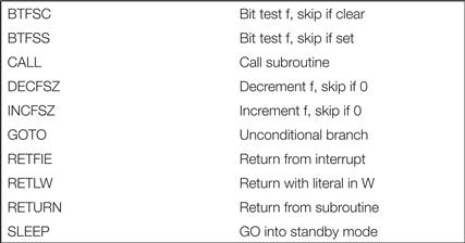
Figure 2.20 Flow of control instructions in the PIC16F.
Subroutines
Subroutines are called using the CALL instruction. The k operand provides the bottom 11 bits of the program counter while the top two come from PCLATH<4:3>. The return address is pushed onto the stack. There are several variations on subroutine return, all of which use the top of the stack as the new PC value. RETURN performs a simple return; RETLW returns with an 8-bit literal k saved in the W register. RETFIE is used to return from interrupts, including enabling interrupts.
2.5 TI C55x DSP
The Texas Instruments C55x DSP is a family of digital signal processors designed for relatively high performance signal processing. The family extends on previous generations of TI DSPs; the architecture is also defined to allow several different implementations that comply with the instruction set.
Accumulator architecture
The C55x, like many DSPs, is an accumulator architecture, meaning that many arithmetic operations are of the form accumulator = operand + accumulator. Because one of the operands is the accumulator, it need not be specified in the instruction. Accumulator-oriented instructions are also well-suited to the types of operations performed in digital signal processing, such as a1 x1 + a2 x2 + …. Of course, the C55x has more than one register and not all instructions adhere to the accumulator-oriented format. But we will see that arithmetic and logical operations take a very different form in the C55x than they do in the ARM.
Assembly language format
C55x assembly language programs follow the typical format:
MPY *AR0, *CDP+, AC0
label: MOV #1, T0
Assembler mnemonics are case-insensitive. Instruction mnemonics are formed by combining a root with prefixes and/or suffixes. For example, the A prefix denotes an operation performed in addressing mode while the 40 suffix denotes an arithmetic operation performed in 40-bit resolution. We will discuss the prefixes and suffixes in more detail when we describe the instructions.
The C55x also allows operations to be specified in an algebraic form:
AC1 = AR0 * coef(*CDP)
2.5.1 Processor and Memory Organization
We will use the term register to mean any type of register in the programmer model and the term accumulator to mean a register used primarily in the accumulator style.
Data types
The C55x supports several data types:
Registers
The C55x has a number of registers. Few to none of these registers are general-purpose registers like those of the ARM. Registers are generally used for specialized purposes. Because the C55x registers are less regular, we will discuss them by how they may be used rather than simply listing them.
Most registers are memory-mapped—that is, the register has an address in the memory space. A memory-mapped register can be referred to in assembly language in two different ways: either by referring to its mnemonic name or through its address.
Program counter and control flow
The program counter is PC. The program counter extension register XPC extends the range of the program counter. The return address register RETA is used for subroutines.
Accumulators
The C55x has four 40-bit accumulators AC0, AC1, AC2, and AC3. The low-order bits 0-15 are referred to as AC0L, AC1L, AC2L, and AC3L; the high-order bits 16-31 are referred to as AC0H, AC1H, AC2H, and AC3H; and the guard bits 32-39 are referred to as AC0G, AC1G, AC2G, and AC3G. (Guard bits are used in numerical algorithms like signal processing to provide a larger dynamic range for intermediate calculations.)
Status registers
The architecture provides six status registers. Three of the status registers, ST0 and ST1 and the processor mode status register PMST, are inherited from the C54x architecture. The C55x adds four registers ST0_55, ST1_55, ST2_55, and ST3_55. These registers provide arithmetic and bit manipulation flags, a data page pointer and auxiliary register pointer, and processor mode bits, among other features.
Stack pointers
The stack pointer SP keeps track of the system stack. A separate system stack is maintained through the SSP register. The SPH register is an extended data page pointer for both SP and SSP.
Auxiliary and coefficient data pointer registers
Eight auxiliary registers AR0-AR7 are used by several types of instructions, notably for circular buffer operations. The coefficient data pointer CDP is used to read coefficients for polynomial evaluation instructions; CDPH is the main data page pointer for the CDP.
Circular buffers
The circular buffer size register BK47 is used for circular buffer operations for the auxiliary registers AR4-7. Four registers define the start of circular buffers: BSA01 for auxiliary registers AR0 and AR1; BSA23 for AR2 and AR3; BSA45 for AR4 and AR5; and BSA67 for AR6 and AR7. The circular buffer size register BK03 is used to address circular buffers that are commonly used in signal processing. BKC is the circular buffer size register for CDP. BSAC is the circular buffer coefficient start address register.
Single repeat registers
Repeats of single instructions are controlled by the single repeat register CSR. This counter is the primary interface to the program. It is loaded with the required number of iterations. When the repeat starts, the value in CSR is copied into the repeat counter RPTC, which maintains the counts for the current repeat and is decremented during each iteration.
Block repeat registers
Several registers are used for block repeats—instructions that are executed several times in a row. The block repeat counter BRC0 counts block repeat iterations. The block repeat start and end registers RSA0L and REA0L keep track of the start and end points of the block.
The block repeat register 1 BRC1 and block repeat save register 1 BRS1 are used to repeat blocks of instructions. There are two repeat start address registers RSA0 and RSA1. Each is divided into low and high parts: RSA0L and RSA0H, for example.
Temporary registers
Four temporary registers T0, T1, T2, and T3 are used for various calculations. These temporary registers are intended for miscellaneous use in code, such as holding a multiplicand for a multiply, holding shift counts, and so on.
Transition registers
Two transition register TRN0 and TRN1 are used for compare-and-extract-extremum instructions. These instructions are used to implement the Viterbi algorithm.
Data and peripheral page pointers
Several registers are used for addressing modes. The memory data page start address registers DP and DPH are used as the base address for data accesses. Similarly, the peripheral data page start address register PDP is used as a base for I/O addresses.
Interrupts
Several registers control interrupts. The interrupt mask registers 0 and 1, named IER0 and IER1, determine what interrupts will be recognized. The interrupt flag registers 0 and 1, named IFR0 and IFR1, keep track of currently pending interrupts. Two other registers, DBIER0 and DBIER1, are used for debugging. Two registers, the interrupt vector register DSP (IVPD) and interrupt vector register host (IVPH), are used as the base address for the interrupt vector table.
The C55x registers are summarized in Figure 2.21.
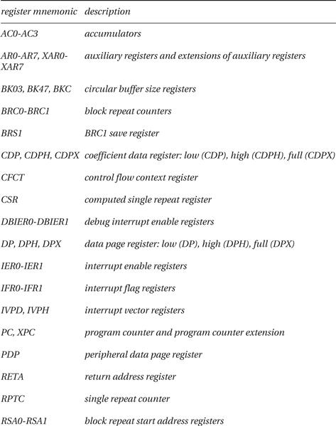
Figure 2.21 Registers in the TI C55x.
Memory map
The C55x supports a 24-bit address space, providing 16 MB of memory, as shown in Figure 2.22. Data, program, and I/O accesses are all mapped to the same physical memory. But these three spaces are addressed in different ways. The program space is byte-addressable, so an instruction reference is 24 bits long. Data space is word-addressable, so a data address is 23 bits. (Its least-significant bit is set to 0.) The data space is also divided into 128 pages of 64K words each. The I/O space is 64K words wide, so an I/O address is 16 bits. The situation is summarized in Figure 2.23.
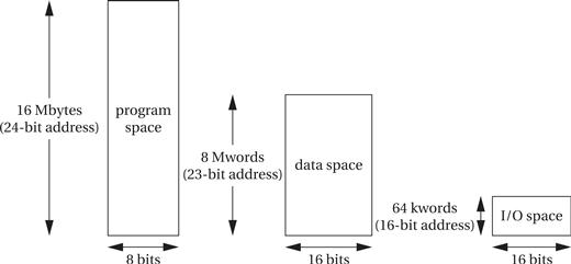
Figure 2.22 Address spaces in the TMS320C55x.
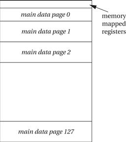
Figure 2.23 The C55x memory map.
Not all implementations of the C55x may provide all 16 MB of memory on chip. The C5510, for example, provides 352 KB of on-chip memory. The remainder of the memory space is provided by separate memory chips connected to the DSP.
The first 96 words of data page 0 are reserved for the memory-mapped registers. Because the program space is byte-addressable, unlike the word-addressable data space, the first 192 words of the program space are reserved for those same registers.
2.5.2 Addressing Modes
Addressing modes
The C55x has three addressing modes:
• Absolute addressing supplies an address in the instruction.
Absolute addressing
Absolute addresses may be any of three different types:
• A k16 absolute address is a 16-bit value that is combined with the DPH register to form a 23-bit address.
• A k23 absolute address is a 23-bit unsigned number that provides a full data address.
• An I/O absolute address is of the form port(#1234), where the argument to port() is a 16-bit unsigned value that provides the address in the I/O space.
Direct addressing
Direct addresses may be any of four different types:

Doffset is calculated by the assembler; its value depends on whether you are accessing a data page value or a memory-mapped register.
Soffset is an offset supplied by the programmer.
• Register-bit direct addressing accesses bits in registers. The argument @bitoffset is an offset from the least-significant bit of the register. Only a few instructions (register test, set, clear, complement) support this mode.
• PDP addressing is used to access I/O pages. The 16-bit address is calculated as
The PDPoffset identifies the word within the I/O page. This addressing mode is specified with the port() qualifier.
Indirect addressing
Indirect addresses may be any of four different types:
• AR indirect addressing uses an auxiliary register to point to data. This addressing mode is further subdivided into accesses into data, register bits, and I/O. To access a data page, the AR supplies the bottom 16 bits of the address and the top 7 bits are supplied by the top bits of the XAR register. For register bits, the AR supplies a bit number. (As with register-bit direct addressing, this only works on the register bit instructions.) When accessing the I/O space, the AR supplies a 16-bit I/O address. This mode may update the value of the AR register. Updates are specified by modifiers to the register identifier, such as adding + after the register name. Furthermore, the types of modifications allowed depend upon the ARMS bit of status register ST2_55: 0 for DSP mode, 1 for control mode. A large number of such updates are possible: examples include *ARn+, which adds 1 to the register for a 16-bit operation and 2 to the register for a 32-bit operation; *(ARn + AR0) writes the value of ARn + AR0 into ARn.
• Dual AR indirect addressing allows two simultaneous data accesses, either for an instruction that requires two accesses or for executing two instructions in parallel. Depending on the modifiers to the register ID, the register value may be updated.
• CDP indirect addressing uses the CDP register to access coefficients that may be in data space, register bits, or I/O space. In the case of data space accesses, the top 7 bits of the address come from CDPH and the bottom 16 come from the CDP. For register bits, the CDP provides a bit number. For I/O space accesses specified with port(), the CDP gives a 16 bit I/O address. Depending on the modifiers to the register ID, the CDP register value may be updated.
• Coefficient indirect addressing is similar to CDP indirect mode, but is used primarily for instructions that require three memory operands per cycle.
Any of the indirect addressing modes may use circular addressing, which is handy for many DSP operations. Circular addressing is specified with the ARnLC bit in status register ST2_55. For example, if bit AR0LC=1, then the main data page is supplied by AR0H, the buffer start register is BSA01, and the buffer size register is BK03.
Stack operations
The C55x supports two stacks: one for data and one for the system. Each stack is addressed by a 16-bit address. These two stacks can be relocated to different spots in the memory map by specifying a page using the high register: SP and SPH form XSP, the extended data stack; SSP and SPH form XSSP, the extended system stack. Note that both SP and SSP share the same page register SPH. XSP and XSSP hold 23-bit addresses that correspond to data locations.
The C55x supports three different stack configurations. These configurations depend on how the data and system stacks relate and how subroutine returns are implemented.
• In a dual 16-bit stack with fast return configuration, the data and system stacks are independent. A push or pop on the data stack does not affect the system stack. The RETA and CFCT registers are used to implement fast subroutine returns.
• In a dual 16-bit stack with slow return configuration, the data and system stacks are independent. However, RETA and CFCT are not used for slow subroutine returns; instead, the return address and loop context are stored on the stack.
• In a 32-bit stack with slow return configuration, SP and SSP are both modified by the same amount on any stack operation.
2.5.3 Data Operations
Move instruction
The MOV instruction moves data between registers and memory:
MOV src,dst
A number of variations of MOV are possible. The instruction can be used to move from memory into a register, from a register to memory, between registers, or from one memory location to another.
The ADD instruction adds a source and destination together and stores the result in the destination:
ADD src,dst
This instruction produces dst = dst + src. The destination may be an accumulator or another type. Variants allow constants to be added to the destination. Other variants allow the source to be a memory location. The addition may also be performed on two accumulators, one of which has been shifted by a constant number of bits. Other variations are also defined.
A dual addition performs two adds in parallel:
ADD dual(Lmem),ACx,ACy
This instruction performs HI(ACy) = HI(Lmem) + HI(ACx) and LO(ACy) = LO(Lmem) + LO(ACx). The operation is performed in 40-bit mode, but the lower 16 and upper 24 bits of the result are separated.
Multiply instructions
The MPY instruction performs an integer multiplication:
MPY src,dst
Multiplications are performed on 16-bit values. Multiplication may be performed on accumulators, temporary registers, constants, or memory locations. The memory locations may be addressed either directly or using the coefficient addressing mode.
A multiply and accumulate is performed by the MAC instruction. It takes the same basic types of operands as does MPY. In the form
MAC ACx,Tx,ACy
the instruction performs ACy = ACy + (ACx * Tx).
Compare instruction
The compare instruction compares two values and sets a test control flag:
CMP Smem == val, TC1
The memory location is compared to a constant value. TC1 is set if the two are equal and cleared if they are not equal.
The compare instruction can also be used to compare registers:
CMP src RELOP dst, TC1
The two registers can be compared using a variety of relational operators RELOP. If the U suffix is used on the instruction, the comparison is performed unsigned.
2.5.4 Flow of Control
Branches
The B instruction is an unconditional branch. The branch target may be defined by the low 24 bits of an accumulator
B ACx
or by an address label
B label
The BCC instruction is a conditional branch:
BCC label, cond
The condition code determines the condition to be tested. Condition codes specify registers and the tests to be performed on them:
• Test the value of an accumulator: <0, <=0, >0, >=0, =0, !=0.
• Test the value of the accumulator overflow status bit.
• Test the value of an auxiliary register: <0, <=0, >0, >=0, =0, !=0.
• Test the value of a temporary register: <0, <=0, >0, >=0, =0, !=0.
• Test the control flags against 0 (condition prefixed by !) or against 1 (not prefixed by !) for combinations of AND, OR, and NOT.
Loops
The C55x allows an instruction or a block of instructions to be repeated. Repeats provide efficient implementation of loops. Repeats may also be nested to provide two levels of repeats.
A single-instruction repeat is controlled by two registers. The single repeat counter, RPTC, counts the number of additional executions of the instruction to be executed; if RPTC = N, then the instruction is executed a total of N + 1 times. A repeat with a computed number of iterations may be performed using the computed single-repeat register CSR. The desired number of operations is computed and stored in CSR; the value of CSR is then copied into RPTC at the beginning of the repeat.
Block repeats perform a repeat on a block of contiguous instructions. A level 0 block repeat is controlled by three registers: the block repeat counter 0, BRC0, holds the number of times after the initial execution to repeat the instruction; the block repeat start address register 0, RSA0, holds the address of the first instruction in the repeat block; the repeat end address register 0, REA0, holds the address of the last instruction in the repeat block. (Note that, as with a single instruction repeat, if BRCn’s value is N, then the instruction or block is executed N + 1 times.)
A level 1 block repeat uses BRC1, RSA1, and REA1. It also uses BRS1, the block repeat save register 1. Each time that the loop repeats, BRC1 is initialized with the value from BRS1. Before the block repeat starts, a load to BRC1 automatically copies the value to BRS1 to be sure that the right value is used for the inner loop executions.
Nonrepeatable instructions
A repeat cannot be applied to all instructions—some instructions cannot be repeated.
Subroutines
An unconditional subroutine call is performed by the CALL instruction:
CALL target
The target of the call may be a direct address or an address stored in an accumulator. Subroutines make use of the stack. A subroutine call stores two important registers: the return address and the loop context register. Both these values are pushed onto the stack.
A conditional subroutine call is coded as:
CALLCC adrs,cond
The address is a direct address; an accumulator value may not be used as the subroutine target. The conditional is as with other conditional instructions. As with the unconditional CALL, CALLCC stores the return address and loop context register on the stack.
The C55x provides two types of subroutine returns: fast-return and slow-return. These vary on where they store the return address and loop context. In a slow return, the return address and loop context are stored on the stack. In a fast return, these two values are stored in registers: the return address register and the control flow context register.
Interrupts
Interrupts use the basic subroutine call mechanism. They are processed in four phases:
1. The interrupt request is received.
2. The interrupt request is acknowledged.
3. Prepare for the interrupt service routine by finishing execution of the current instruction, storing registers, and retrieving the interrupt vector.
4. Processing the interrupt service routine, which concludes with a return-from-interrupt instruction.
The C55x supports 32 interrupt vectors. Interrupts may be prioritized into 27 levels. The highest-priority interrupt is a hardware and software reset.
Most of the interrupts may be masked using the interrupt flag registers IFR1 and IFR2. Interrupt vectors 2-23, the bus error interrupt, the data log interrupt, and the real-time operating system interrupt can all be masked.
2.5.5 C Coding Guidelines
Some coding guidelines for the C55x [Tex01] not only provide more efficient code but in some cases should be paid attention to in order to ensure that the generated code is correct.
As with all digital signal processing code, the C55x benefits from careful attention to the required sizes of variables. The C55x compiler uses some nonstandard lengths of data types: char, short, and int are all 16 bits, long is 32 bits, and long long is 40 bits. The C55x uses IEEE formats for float (32 bits) and double (64 bits). C code should not assume that int and long are the same types, that char is 8 bits long or that long is 64 bits. The int type should be used for fixed-point arithmetic, especially multiplications, and for loop counters.
The C55x compiler makes some important assumptions about operands of multiplications. This code generates a 32-bit result from the multiplication of two 16-bit operands:
long result = (long)(int)src1 * (long)(int)src2;
Although the operands were coerced to long, the compiler notes that each is 16 bits, so it uses a single-instruction multiplication.
The order of instructions in the compiled code depends in part on the C55x pipeline characteristics. The C compiler schedules code to minimize code conflicts and to take advantage of parallelism wherever possible. However, if the compiler cannot determine that a set of instructions are independent, it must assume that they are dependent and generate more restrictive, slower code. The restrict keyword can be used to tell the compiler that a given pointer is the only one in the scope that can point to a particular object. The -pm option allows the compiler to perform more global analysis and find more independent sets of instructions.
Example 2.8 shows a C implementation of an FIR filter on the C55x.
Example 2.8 FIR Filter on the C55x
Here is assembly code generated by the TI C55x C compiler for the FIR filter with manually generated comments:
MOV AR0, *SP(#1) ; set up the loop
MOV T0, *SP(#0)
MOV #0, *SP(#2)
MOV #0, *SP(#3)
MOV *SP(#2), AR1
|| MOV #8, AR2
CMP AR1 >= AR2, TC1
|| NOP ; avoids Silicon Exception CPU_24
BCC $C$L2,TC1
; loop body
$C$L1:
$C$DW$L$_main$2$B:
MOV SP, AR3 ; copy stack pointer into auxiliary registers for address computation
MOV SP, AR2
MOV AR1, T0
AMAR *+AR3(#12) ; set up operands
ADD *SP(#2), AR3, AR3
MOV *SP(#3), AC0 ; put f into auxiliary register
AMAR *+AR2(#4)
MACM *AR3, *AR2(T0), AC0, AC0 ; multiply and accumulate
MOV AC0, *SP(#3) ; save f on stack
ADD #1, *SP(#2) ; increment loop count
MOV *SP(#2), AR1
|| MOV #8, AR2
CMP AR1 < AR2, TC1
|| NOP ; avoids Silicon Exception CPU_24
BCC $C$L1,TC1
; return for next iteration
2.6 TI C64x
The Texas Instruments TMS320C64x is a high-performance VLIW DSP. It provides both fixed-point and floating-point arithmetic. The CPU can execute up to eight instructions per cycle using eight general-purpose 32-bit registers and eight functional units.
Figure 2.24 shows a simplified block diagram of the C64x. Although instruction execution is controlled by a single execution unit, the instructions are performed by two data paths, each with its own register file. The CPU is a load/store architecture. The data paths are named A and B. Each data path provides four function units:
• The .L units (.L1 and .L2 in the two data paths) perform 32/40-bit arithmetic and comparison, 32-bit logical, and data packing/unpacking.
• The .S units (.S1 and .S2) perform 32-bit arithmetic, 32/40-bit shifts and bit-field operators, 32-bit logical operators, branches, and other operations.
• The .M units (.M1 and .M2) perform multiplications, bit interleaving, rotation, Galois field multiplication, and other operations.
• The .D units (.D1 and .D2) perform address calculations, loads and stores, and other operations.
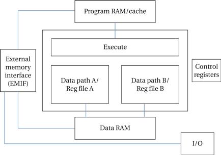
Figure 2.24 C64x block diagram.
Separate data paths perform data movement:
• Load-from memory units .LD1 and .LD2. These units loads registers from memory.
• Store-from memory units .ST1 and .ST2 to store register values to memory.
• Address paths .DA1 and .DA2 to compute addresses. These units are associated with the .D1 and .D2 units in the data paths.
• Register file cross paths .1X and .2X to move data between register files A and B. Data must be explicitly moved from one register file to the other before it can be used in the other data path.
On-chip memory is organized as separate data and program memories. The external memory interface (EMIF) manages connections to external memory. The external memory is generally organized as a unified memory space.
The C64x provides a variety of 40-bit operations. A 40-bit value is stored in a register pair, with the least significant bits in an even-numbered register and the remaining bits in an odd-numbered register. A similar scheme is used for 64-bit values.
Instructions are fetched in groups known as fetch packets. A fetch packet includes eight words at a time and is aligned on 256-bit boundaries. Due to the small size of some instructions, a fetch packet may include up to 14 instructions. The instructions in a fetch packet may be executed in varying combinations of sequential and parallel execution. An execute packet is a set of instructions that execute together. Up to eight instructions may execute together in a fetch packet, but all must use a different functional unit, either performing different operations on a data path or using corresponding function units in different data paths. The p-bit in each instruction encodes information about which instructions can be executed in parallel. Instructions may execute fully serially, fully parallel, or partially serially.
Many instructions can be conditionally executed, as specified by a s that specifies the condition register and a z field that specifies a test for zero or nonzero.
Two instructions in the same execute packet cannot use the same resources or write to the same register on the same cycle. Here are some examples of these constraints:
• Instructions must use separate functional units. For example, two instructions cannot simultaneously use the .S1 unit.
• Most combinations of writing using the same .M unit are prohibited.
• Most cases of reading multiple values in the opposite register file using the .1X and .2X cross path units are prohibited.
• A delay cycle is executed when an instruction attempts to read a register that was updated in the previous cycle by a cross path operation.
• The .DA1 and .DA2 units cannot execute in one execute packet two load and store registers using a destination or source from the same register file. The address register must be in the same data path as the .D unit being used.
• At most four reads of the same register can occur on the same cycle.
• Two instructions in an execute packet cannot write to the same register on the same cycle.
• A variety of other constraints limit the combinations of instructions that are allowed in an execute packet.
The C64x provides delay slots, which were first introduced in RISC processors. Some effects of an instruction may take additional cycles to complete. The delay slot is a set of instructions following the given instruction; the delayed results of the given instruction are not available in the delay slot. An instruction that does not need the result can be scheduled within the delay slot. Any instruction that requires the new value must be placed after the end of the delay slot. For example, a branch instruction has a delay slot of five cycles.
The C64x provides three addressing modes: linear, circular using BK0, and circular using BK1. The addressing mode is determined by the AMR addressing mode register. A linear address shifts the offset by 3, 2, 1, or 0 bits depending on the length of the operand, then adds the base register to determine the physical address. The circular addressing modes using BK0 and BK1 use the same shift and base calculation but only modify bits 0 through N of the address.
The C64x provides atomic operations that can be used to implement semaphores and other mechanisms for concurrent communication. The LL (load linked) instruction reads a location and sets a link valid flag to true. The link valid flag is cleared when another process stores to that address. The SL (store linked) instruction prepares a word to be committed to memory by storing it in a buffer but does not commit the change. The commit linked stores CMTL instruction checks the link valid flag and writes the SL-buffered data if the flag is true.
The processing of interrupts is mediated by registers. The interrupt flag register IFR is set when an interrupt occurs; the ith bit of IFR corresponds to the ith level of interrupt. Interrupts are enabled and disabled using the interrupt enable register IER. Manual interrupts are controlled using the interrupt set register ISR and interrupt clear register ICR. The interrupt return pointer register IRP contains the return address for the interrupt. The interrupt service table pointer register ISTP points to a table of interrupt handlers. The processor supports nonmaskable interrupts.
The C64x+ is an enhanced version of the C64x. It supports a number of exceptions. The exception flag register EFR indicates which exceptions have been thrown. The exception clear register ECR can be used to clear bits in the EFR. The internal exception report register IERR indicates the cause of an internal exception. The C64x+ provides two modes of program execution, user and supervisor. Several registers, notably those related to interrupts and exceptions, are not available in user mode. A supervisor mode program can enter user mode using the B NRP instruction. A user mode program may enter supervisor mode by using an SWE or SWENR software interrupt.
2.7 Summary
When viewed from high above, all CPUs are similar—they read and write memory, perform data operations, and make decisions. However, there are many ways to design an instruction set, as illustrated by the differences between the ARM, the C55x, and the C64x. When designing complex systems, we generally view the programs in high-level language form, which hides many of the details of the instruction set. However, differences in instruction sets can be reflected in nonfunctional characteristics, such as program size and speed.
What we Learned
• Both the von Neumann and Harvard architectures are in common use today.
• The programming model is a description of the architecture relevant to instruction operation.
• ARM is a load-store architecture. It provides a few relatively complex instructions, such as saving and restoring multiple registers.
• The PIC16F is a very small, efficient microcontroller.
• The C55x provides a number of architectural features to support the arithmetic loops that are common on digital signal processing code.
• The C64x organizes instructions into execution packets to enable parallel execution.
Further reading
Books by Jaggar [Jag95], Furber [Fur96], and Sloss et al. [Slo04] describe the ARM architecture. The ARM Web site, http://www.arm.com, contains a large number of documents describing various versions of ARM. Information on the PIC16F can be found at www.microchip.com. Information on the C55x and C64x can be found at http://www.ti.com.
Questions
Q2-1 What is the difference between a big-endian and little-endian data representation?
Q2-2 What is the difference between the Harvard and von Neumann architectures?
Q2-3 Answer the following questions about the ARM programming model:
a. How many general-purpose registers are there?
b. What is the purpose of the CPSR?
Q2-4 How would the ARM status word be set after these operations?
Q2-5 What is the meaning of these ARM condition codes?
Q2-6 Explain the operation of the BL instruction, including the state of ARM registers before and after its operation.
Q2-7 How do you return from an ARM procedure?
Q2-8 In the following code, show the contents of the ARM function call stack just after each C function has been entered and just after the function exits. Assume that the function call stack is empty when main() begins.
int foo(int x1, int x2) {
return x1 + x2;
}
int baz(int x1) {
return x1 + 1;
}
int scum(int r) {
for (i = 0; i = 2; i++)
foo(r + i,5);
}
main() {
scum(3);
baz(2);
m}
Q2-9 Why are specialized instruction sets such as Neon or Jazelle useful?
Q2-10 Is the PIC16F a general-purpose register machine?
Q2-11 How large is the program counter stack in the PIC16F?
Q2-12 What two registers contribute to the program counter value?
Q2-13 What data types does the C55x support?
Q2-14 How many accumulators does the C55x have?
Q2-15 What C55x register holds arithmetic and bit manipulation flags?
Q2-16 What is a block repeat in the C55x?
Q2-17 How are the C55x data and program memory arranged in the physical memory?
Q2-18 Where are C55x memory-mapped registers located in the address space?
Q2-19 What is the AR register used for in the C55x?
Q2-20 What is the difference between DP and PDP addressing modes in the C55x?
Q2-21 How many stacks are supported by the C55x architecture and how are their locations in memory determined?
Q2-22 What register controls single-instruction repeats in the C55x?
Q2-23 What is the difference between slow and fast returns in the C55x?
Q2-24 How many functional units does the C64x have?
Q2-25 What is the difference between a fetch packet and an execute packet in the C64x?
Lab exercises
L2-1 Write a program that uses a circular buffer to perform FIR filtering.
L2-2 Write a simple loop that lets you exercise the cache. By changing the number of statements in the loop body, you can vary the cache hit rate of the loop as it executes. You should be able to observe changes in the speed of execution by observing the microprocessor bus.
L2-3 Compare the implementations of an FIR filter on two different processors. How do they compare in code size and performance?