12
Isolated DC‐DC Converters
In this chapter‚ the reader is introduced to isolated dc‐dc power converters. Isolated power converters enable safe and efficient power conversion and play key EV roles in the charging of batteries and the powering of auxiliary loads. This chapter introduces the isolated forward converter as a transformer‐based buck converter and then introduces the full‐bridge power converter as the main on‐vehicle isolated power converter. Resonant converters play a significant role in power conversion, especially for inductive and wireless charging, and so the resonant LCLC full‐bridge power converter is presented. Finally, the ubiquitous flyback converter, based on the buck‐boost topology and widely used for lower power levels, is briefly introduced in Appendix II at the back of this chapter.
12.1 Introduction
In this chapter, isolated power converters are introduced and analyzed. These isolated converters are derived from the basic non‐isolated power converter topologies discussed in Chapter 11.
12.1.1 Advantages of Isolated Power Converters
Transformer‐isolated converters are required in applications for the following very fundamental reasons.
Safety
Electrical systems can present safety hazards to the consumer, and the risks are greater at higher voltages. In general, voltages below 40 V to 60 V are regarded as safe, but the levels can be lower depending on the conditions. Electric vehicles generally have high‐voltage battery packs of about 400 V, and significant protections must be incorporated into the vehicle power architecture in order to ensure safe operation. The principal method to ensure a physical and electrical barrier between the high and low voltages is to use a transformer to provide galvanic isolation.
Efficiency
When significant voltage conversions are required, such as converting from a high‐voltage battery at 400 V to the 12 V level required for on‐vehicle accessory loads, it is necessary to use a transformer in order to optimally design and size a practical switch‐mode power converter. The transformer‐based circuits have reduced peak, mean, and rms currents, resulting in improved efficiency, better control, reduced voltage stresses, and reduced electromagnetic interference.
Multiple Outputs
There are many different low‐voltage loads on the vehicle requiring different voltage levels such as the windshield defrost at 42 V and the accessory battery at 12 V. Similarly, there can be multiple voltage levels used in a smartphone or computer. The simplest way to provide multiple voltage outputs is to use a transformer with multiple secondary windings.
12.1.2 Power Converter Families
There are three main families of isolated power converters which are commonly used. These families are based on the buck converter, the buck‐boost converter, and the resonant converter.
The common buck‐derived converters are the forward converter, which is used for low to medium power, in the range 50 to 200 W, and the full bridge, which is used for high power, from about 200 W to many kilowatts. There are many variations on forward and full‐bridge converters. For example, single‐switch and two‐switch forward converters can be used. The commonly used full‐bridge converters are the hard‐switched and the phase‐shifted variations. Both types of full‐bridge converters play a role on the vehicle. This chapter focuses on the basic hard‐switched converter due to its relative simplicity. Other closely related variants are the push‐pull and half‐bridge converters. The forward converter is presented for teaching purposes in this chapter as it is based on the buck converter and links the buck and the full‐bridge converters.
An example of an automotive full‐bridge auxiliary power converter is shown in Figure 12.1, where the symbol Q marks the power switches, X marks the transformer, and L marks the output inductor. The high‐voltage input terminals and the low‐voltage output terminals are labeled HVIP and LVOP, respectively. The electromagnetic interference (EMI) stage is appropriately marked and features two common‐mode filter inductors (LCM) and several capacitors (cap).

Figure 12.1 Automotive auxiliary power converter for a Ford vehicle.
The transformer‐isolated buck‐boost converter is known as the flyback. The flyback converter is ubiquitous in the modern world and is typically the converter of choice for power converters at powers ranging from milliwatts to a couple of hundred watts. Again, there are many variations on flybacks, and the optimum topology can depend on the application. As the flyback converter is not used for high‐power circuits, it is not discussed in the main chapter but it is briefly covered in Appendix II of this chapter.
Resonant converters have assumed a greater role in isolated power conversion over the last few decades. One of the first significant applications for resonant converters was as the power conversion stage for the inductive charging developed for the GM EV1 program in the mid 1990s [1–2]. The inductive power converters developed for EV charging at the time ranged from 1.5 kW to 130 kW. The resonant converter possesses particular attributes which make it very suitable for wireless power transfer. In the meantime, a class of resonant converters, known as the LLC converter, has been widely adapted for commercial and industrial power conversion [3].
12.2 The Forward Converter
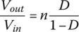
The buck converter is redrawn in Figure 12.2(a) to show a resistive load RO, and the labeling of the various components has been modified. The forward converter is derived from the buck converter, and the basic topology is as shown in Figure 12.2(b).
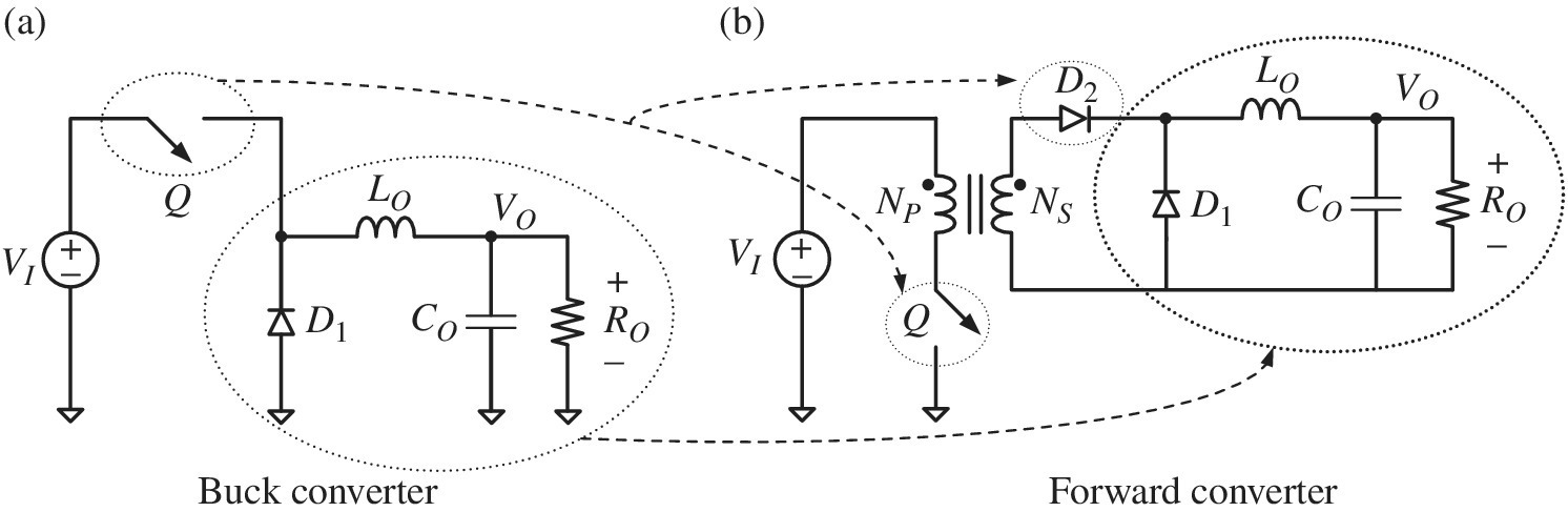
Figure 12.2 (a) Buck converter and (b) idealized forward converter.
The output stage of the forward converter, with components RO, LO, CO, and D1, are identical to the redrawn buck.
The transformer is introduced to the circuit to create the forward converter. From a power and switch perspective, it does not matter whether the switch Q is placed between the positive terminal of the transformer and the input voltage supply or between the negative terminal and the dc return. However, placing the switch between the negative terminal and the dc return makes the control of the switch simpler to implement, and so the switch location is typically as in the diagram.
The introduction of the transformer requires an additional diode D2 to ensure that the transformer only conducts when the primary‐side switch Q conducts.
A problem arises with the forward converter as shown in Figure 12.2(b). A transformer must be magnetized in order to operate as a transformer, as discussed in Chapter 16, Section 16.5. The magnetization is usually represented by a primary‐side magnetizing inductance. However, the magnetizing inductance must be demagnetized each cycle when the primary‐side switch is not conducting in order to avoid core saturation. The demagnetization in a forward converter is achieved by adding a third winding, often known as the tertiary winding NT, and a diode D3 so that the transformer demagnetizes when the switch stops conducting, as shown in Figure 12.3. The requirement to demagnetize the transformer puts a practical maximum limit on the duty cycle D of the primary‐side switch. Typically, the tertiary winding has the same number of turns as the primary and is closely coupled to the primary winding in a bifilar winding. The maximum duty cycle is typically 0.5 for this condition of equal primary and tertiary turns.
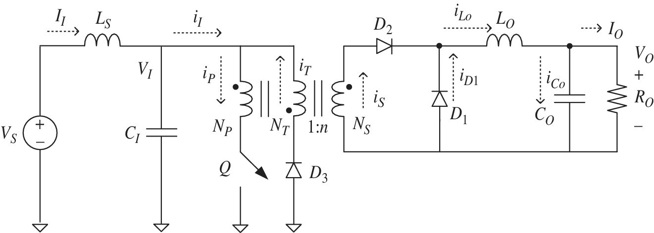
Figure 12.3 Forward converter.
The input source voltage VS is also shown as having an internal inductance LS. In this chapter, for simplicity, the source inductance and filter capacitance CI are neglected, and the input is simply modeled as a voltage source VI. The procedure of Chapter 11 can be used to determine the input capacitor current and voltage ripple.
It is worth investigating the operation of the forward converter in additional detail to illustrate the transformer action. There are three operating modes when operating in continuous conduction mode (CCM). When the switch Q is closed in the first mode, as shown in Figure 12.4(i), the magnetizing current im builds up in the magnetizing inductance Lm, and a reflected secondary current is ′ flows by transformer action, induced by the secondary current is. No current flows in the tertiary winding when the switch is closed, and diode D1 does not conduct in this mode as it is reverse biased.
Figure 12.4 Forward converter CCM modes.
In the second mode, as shown in Figure 12.4(ii), the switch Q is open, and the primary winding no longer conducts current. However, there is energy stored in the magnetizing inductance, which forces the tertiary magnetizing current iT to flow in the tertiary winding by coupled‐inductor transformer action, until the transformer is demagnetized. There is no secondary current due to the reverse‐biased D2, and the output current is supplied from the energy stored in LO through D1.
In the third mode, as shown in Figure 12.4(iii), there is no current in any of the transformer windings. The inductor current continues to flow through D1.
12.2.1 CCM Currents in Forward Converter
The duty cycle for the CCM buck converter, discussed in Chapter 11, is equal to the ratio of the output voltage to the input voltage. The presence of the transformer results in the duty cycle for the forward converter being the ratio of the output or secondary volts/turn to the input or primary volts/turn, as follows:
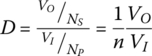
where n is the turns ratio of the transformer NS/NP.
The output inductor waveforms for the forward converter are shown in Figure 12.5. The waveforms can be analyzed in a similar manner to the buck converter. As with the earlier converters, the change in peak‐to‐peak current can provide the basis for converter analysis. All device parasitics are ignored in order to simplify the analysis.
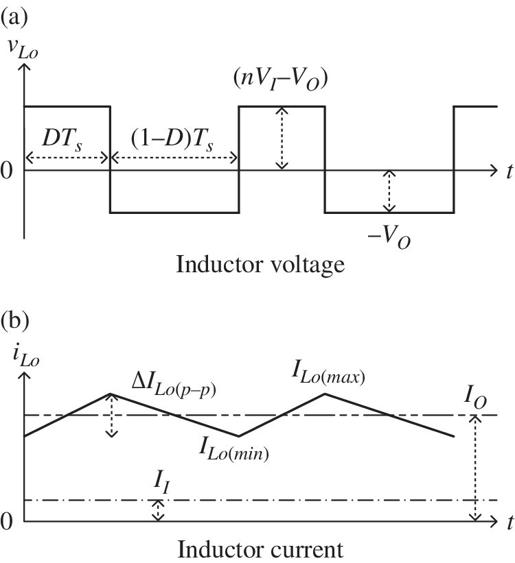
Figure 12.5 Output inductor waveforms for CCM forward converter.
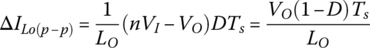
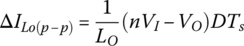
Assuming that the inductor current is changing linearly in steady‐state operation, then the change in current from peak to peak can be described by ΔILo(p‐p).
During time DTs, where Ts is the period:
During time (1‐D)Ts:
Equating the two expressions for the current ΔILo(p‐p):
Solving the two equations again yields the earlier expression for the relationship between the duty cycle and voltage gain in Equation (12.1).
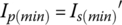
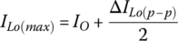
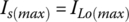
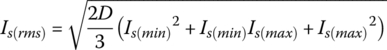
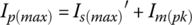
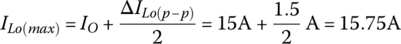
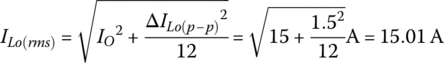
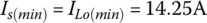
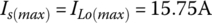
The currents in the various components are illustrated in Figure 12.6 and are determined as follows. Diode D2 conducts when the switch is conducting, and the current in D2 is the secondary current is. The current changes from a minimum level Is(min) to a maximum level Is(max) over the cycle, and these values are given by
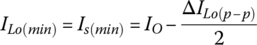
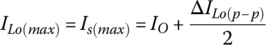

Figure 12.6 Forward converter CCM waveforms.
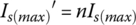
The secondary current is reflected to the primary using the transformer turns ratio:

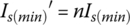
Thus, the minimum and maximum reflected secondary currents, Is(min)′ and Is(max)′, are given by

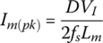
The magnetizing current builds up while the switch is closed, as shown in Figure 12.4(i). The switch conducts for DTs, and the voltage across the inductance is VI. Thus, the voltage across the magnetizing inductance vLm is
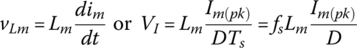
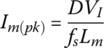
The magnetizing current increases from zero to the peak value of the magnetizing current Im(pk), given by
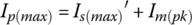
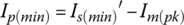
The minimum and maximum primary and transistor currents are the sum of the magnetizing and reflected secondary currents and are given by
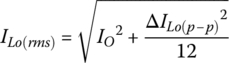
Knowing all these currents, the rms and average values for all components in the converter can be determined (See Appendix I). All the waveforms shown in Figure 12.6(b)–(h) are periodic discontinuous ramp waveforms.
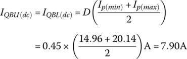
12.2.1.1 Example: Current Ratings in Medium‐Power Forward Converter
A single‐switch forward converter is designed for the following specifications (which are typical practical values for the power level): input voltage of 200 V, output voltage of 12 V, output power of 180 W, switching frequency of 100 kHz, and a magnetizing inductance of 2 mH.
- Size the output inductor for a peak‐to‐peak current ripple ri = 10% at full load.
- Determine the various component currents.
Assume a unity turns ratio between the primary and tertiary windings and a maximum duty cycle of 50% at 200 V.
Ignore all losses, device voltage drops, and the effects of leakage.
Solution:
- The secondary‐primary turns ratio is determined by assuming that the converter operates at the maximum duty cycle of 50% at the minimum input voltage of 200 V. Thus, from Equation (12.1):
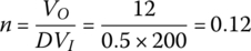
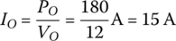
- The dc output current is the output power divided by the output voltage:
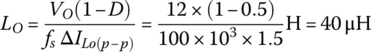
- The peak‐to‐peak output inductor ripple current is

- The output inductance is obtained by rearranging Equation (12.3) to get
- The dc output current is the output power divided by the output voltage:
- The minimum and maximum secondary currents are given by


- The rms current in the inductor can be determined using (11.15) as follows:
- The rms and average currents in diode D2 are
and
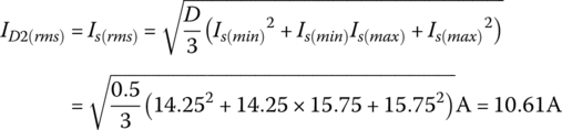

- The rms current in the inductor can be determined using (11.15) as follows:
The rms and average currents in diode D1 are
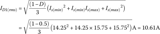
and

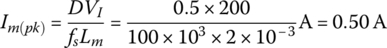
The peak value of the magnetizing current is given by Equation (12.11):
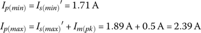
Thus, the reflected secondary transistor currents are


The primary and transistor currents are the sum of the reflected secondary current and the magnetizing current:
The rms and average currents in switch Q are

and

Finally, the rms and average currents in the tertiary winding are
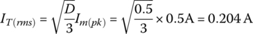
and
where a turns ratio of unity is assumed between the primary and tertiary windings, causing the tertiary windings to demagnetize over the same time interval DTs that the magnetizing current took to build up when the switch was closed.
12.2.2 CCM Voltages in Forward Converter
Significant constraining factors for a single‐switch forward converter are the relatively high voltages across the various semiconductor devices. The voltages across the various components are shown in Figure 12.7(a)–(d). The circuits of Figure 12.4 are repeated as Figure 12.7(i)–(iii).

Figure 12.7 Forward converter voltage waveforms.
As shown in Figure 12.7(a), the voltage across the output inductor vL is the difference between the reflected input voltage and the output voltage.
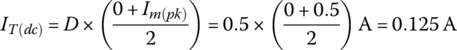
As shown in Figure 12.7(b), the voltage across the transformer primary vpri equals the input voltage when the switch is closed, as seen from Figure 12.7(i). The voltage across the switch is shown in Figure 12.7(c). The voltage is very low when the switch is conducting current, but the voltage increases to VQ(max) when the switch stops conducting, and the tertiary winding conducts. The primary winding voltage is the reflected tertiary voltage when the tertiary winding is conducting current and being demagnetized, as seen from Figure 12.7(ii). These modes of operation result in significant voltage drops across both the transformer winding and the semiconductors. Thus, there are three voltages adding up across the switch when it is off. These are the input voltage itself VI, the reflected tertiary voltage  , and the additional overshoot in the switch VQ(OS) due to the leakage inductances of the circuit and transformer.
In equation form, the maximum voltage across the switch VQ(max) is
It is necessary to derate semiconductor devices in order to operate the devices safely. A reasonable derating is to operate the device at up to 80% of the rated voltage. Thus, the rated voltage VQ(rated) of the switch can be determined from

The other semiconductor components also experience relatively high voltages. The voltage across the output diode D1 is shown in Figure 12.7(d). The maximum voltage across the diode VD1(max) is

where VD1(OS) is the overshoot voltage across D1.
12.2.2.1 Example: Voltage Ratings in a Medium‐Power Forward Converter
The forward converter in the previous example has an input voltage range from 200 to 400 V.
Assume an overshoot of 100 V on the switch and 10 V on the secondary diodes for the forward converter used in the previous example.
Determine the maximum voltages seen by the devices.
What are reasonable rated voltages for these semiconductor components?
Solution:
The maximum voltage across the switch occurs at the maximum input voltage of 400 V:

where a primary‐tertiary turns ratio of unity is assumed.
The minimum rated voltage of the device is

Thus, a rated voltage of 1200 V, when rounded up to the nearest 100 V, would be appropriate for the switch when derated.
The secondary diode experiences a maximum voltage of

The minimum rated voltage of the diode is

Thus, a rated voltage of 80 V, when rounded to the nearest 10 V, would be appropriate for the diode when derated.
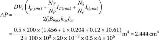
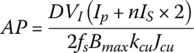
12.2.3 Sizing the Transformer
As discussed in Chapter 16, Section 16.5.3, the area product (AP) for a transformer fed by a duty cycle controlled voltage source supplying a transformer is
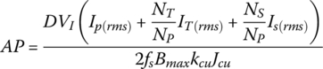
where Bmax is the maximum flux density, kcu is the copper fill factor, and Jcu is the current density.
12.2.3.1 Example: AP of a Forward Converter Transformer
A transformer has the following parameters: copper fill factor kcu = 0.5, current density Jcu = 6A/mm2, and maximum core flux density Bmax = 20 mT. The maximum core flux density is significantly lower than the value used in the examples in Chapter 11 as the high‐frequency transformer is likely to be limited in size by its core loss.
Determine the AP for the transformer in the previous example.
Solution:
The AP is given by
12.3 The Full‐Bridge Converter
The isolated full‐bridge converter is the preferred topology for medium to high power, and is often the topology used on vehicles for charging the high‐voltage battery and powering the low‐voltage auxiliary loads. The relative voltage and current stresses of the full‐bridge converter are lower than those of the forward converter, at the expense of additional components and complexity. The advantages are as follows: the full bridge has twice the power for the same current ratings, half the voltage on the switches, and twice the ripple frequency. On the downside, the full bridge has more semiconductors, and requires isolated gate drives with the danger of shoot‐through.
The basic circuit topologies are shown in Figure 12.8. The full bridge features four semiconductor switches, each partnered with an inverse diode. The full bridge has two poles, A and B, and upper (U) and lower (L) switches and diodes. The full bridge is switched such that an ac square wave voltage appears across the primary of the transformer. For low‐voltage applications, the transformer has two secondary windings which are center‐tapped to connect to the output, as shown in Figure 12.8(a). This ensures that the output current only conducts through one diode at a time – resulting in improved efficiency. For high‐voltage output applications, the relative effect of a diode drop on efficiency is not as significant, and a standard transformer with a single secondary can be connected to a full‐bridge diode rectifier, as shown in Figure 12.8(b). The center‐tapped rectifier, often featuring a low‐conduction‐drop Schottky diode, is suitable for auxiliary power converters outputting 12 V, whereas the full‐bridge rectifier is suitable for high‐voltage battery chargers with outputs of hundreds of volts. Note that a synchronous rectifier is often used for low‐voltage outputs. A synchronous rectifier uses a controlled switch such as a MOSFET to replace the output diode. A low‐voltage MOSFET can have a significantly lower conduction drop than a silicon or Schottky diode.
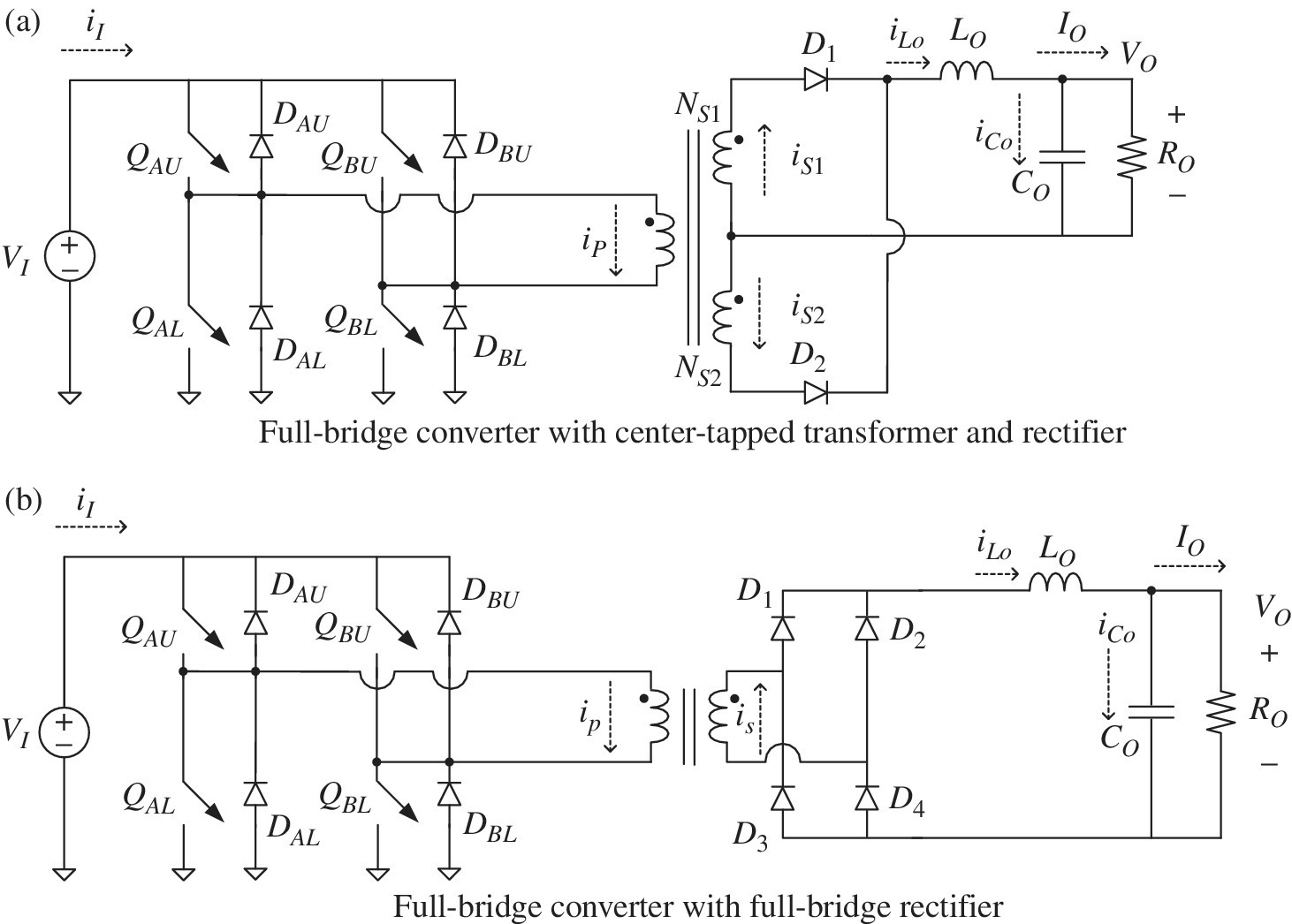
Figure 12.8 Full‐bridge converters.
For both types of converters, the inductor current is filtered by an output capacitor such that dc waveforms are output from the converter. The load is represented generically by a resistor but could be a battery pack or the various auxiliary loads on a vehicle.
There are a number of full‐bridge control schemes which can be used depending on the application. In this chapter, the basic hard‐switched full bridge is considered. The phase‐shifted full bridge is commonly used but is more complex [4].
12.3.1 Operation of Hard‐Switched Full‐Bridge Converter
There are four principal operating modes, labeled I to IV in Figure 12.9, Figure 12.10, and Figure 12.11. The switches are switched on and off according to the patterns shown in Figure 12.9. The pole A upper and lower switches, QAU and QAL, alternate on and off, and both have a 50% duty cycle. The duty cycles of the pole B upper and lower switches, QBU and QBL, are controlled to regulate the output voltage.
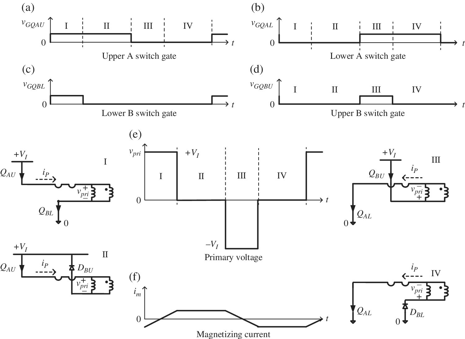
Figure 12.9 Gate voltages, switch configurations, primary voltage, and magnetizing current waveforms.
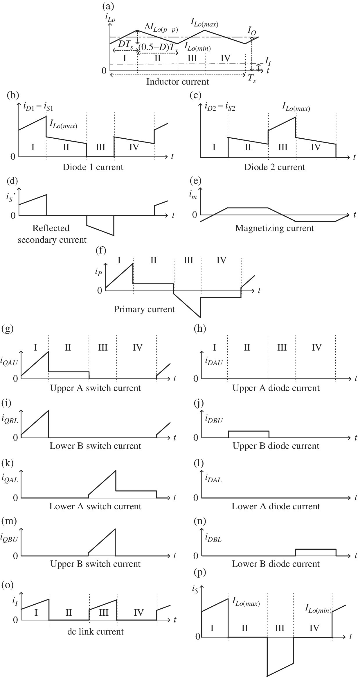
Figure 12.10 Full‐bridge converter CCM current waveforms.

Figure 12.11 Principal modes for hard‐switched full‐bridge converter with (a) center tap and (b) full‐bridge rectifier.
Modes I and II occur during the first half of the switching period. In mode I, gating signals are sent to switches QAU and QBL, as shown in Figure 12.9(a) and (c). This results in a positive voltage across the primary of the transformer, as shown in Figure 12.9(e). When QBL is turned off in mode II, diode DBU becomes forward biased and maintains the primary magnetizing current flow. It is noteworthy that the magnetizing current in the transformer, as shown in Figure 12.9(f), ramps up and down when a net voltage is applied across the primary, but the magnetizing current remains constant when there is no applied voltage – as is expected from Faraday’s law. Modes III and IV occur during the second half of the switching period. In mode III, gating signals are sent to switches QAL and QBU, as shown in Figure 12.9(b) and (d). This results in a negative voltage across the primary of the transformer. When QBU is turned off in mode IV, diode DBL becomes forward biased and maintains the primary current flow. The switch and diode conductions in the various modes are noted in Table 12.1.
Table 12.1 Switch and diode conduction.
| Mode | A‐leg | B‐leg |
| I | QAU | QBL |
| II | DBU | |
| III | QAL | QBU |
| IV | DBL |
The complete set of current waveforms is shown in Figure 12.10.
The output inductor sees a positive voltage reflected from the primary during modes I and III, resulting in a build‐up of current in the output inductor, as shown in Figure 12.10(a).
In mode I, in the case of the center‐tapped converter, the positive voltage across the secondary winding S1 forward‐biases the output diode D1. In the case of the full‐bridge rectifier, output diodes D1 and D4 are both forward‐biased and conduct. See Figure 12.11(a) for mode I circuits.
In mode II, the gating signal is removed from QBL while QAU remains on. See Figure 12.11(b) for mode II circuits. The current which was flowing through QBL now flows through DBU, and the net voltage across the transformer primary is zero. As there is no net voltage across the primary, the magnetizing current remains constant. Switch QBL experiences a hard turn‐off as there is a current flowing through the switch while it is gated off. The action on the secondary side is quite interesting. For both types of converters, the inductor current remains flowing and forward‐biases both sets of output diodes such that equal currents flow in each winding, and there is no net voltage across the transformer secondary or primary. The inductor current decreases as the inductor’s stored energy decreases due to the current flow to the load. The inductor back emf is correspondingly negative.
Mode III is similar to mode I, but the other two switches are activated in order to demagnetize the transformer and to forward‐bias output diode D2 for the center‐tapped converter and diodes D2 and D3 for the full bridge. The switch from QBU experiences a hard turn‐off.
Mode IV is similar to mode II with the difference that the transformer primary is connected to the return of the input. All output diodes again conduct.
12.3.2 CCM Currents in Full‐Bridge Converter
Please note the rms and average formulas for discontinuous ramp and step waveforms presented in the Appendix I of this chapter.
The duty cycle can be derived on the basis of the inductor current. Assuming that the inductor current is changing linearly in the steady‐state operation, the change in current from peak to peak can be described by ΔILo(p‐p). It is important to note that the switching period covers the durations of the four modes, as shown in Figure 12.10(a).
The current increases during time DTs:
and decreases during time (0.5‐D)Ts:
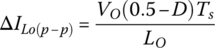
Equating the two expressions for the current ΔILo(p‐p):
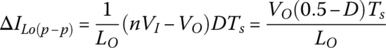
Solving the two equations results in the following expression for the relationship between duty cycle and voltage gain:

where n is the turns ratio of the transformer, n = NS1/NP = NS2/NP for the center‐tapped transformer, and n = NS/NP for the full‐bridge rectifier.
The current waveforms for the full‐bridge converter are shown in Figure 12.10. The waveforms can be analyzed in a similar manner to the forward converter. Similar to the earlier converter, the change in peak‐to‐peak current can provide the basis for converter analysis. As noted in Equation (12.21), the change in the inductor peak‐to‐peak current is easily determined.
The inductor current changes from a minimum to a maximum over the half cycle, and these values are given by
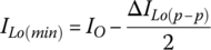
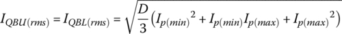
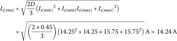
The rms current in the inductor is
The minimum and maximum secondary currents are given by

Let DO represent the output diodes for either rectifier type.
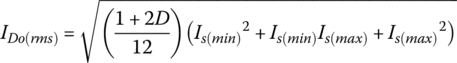
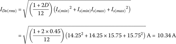
The output diode current has three conduction segments within the period, modes I, II, and IV or modes II, III, and IV. The related rms value of the diode current IDo(rms) is given:

which simplifies to
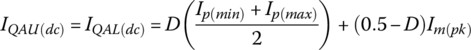
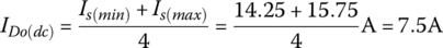
The average value of the diode current IDo(dc) is

an expression which makes sense as the average current in each diode is equal to half the average inductor current.
Note that in the center‐tapped converter, the secondary rms current in one winding is the same as the output diode current:

However, in the full‐bridge rectifier, the secondary current only flows during modes I and III, as shown by the waveform in Figure 12.10(p).
Thus, for the full‐bridge rectifier:
The minimum and maximum reflected secondary currents are given by

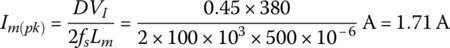
The peak value of the magnetizing current is half the peak‐to‐peak value and is given by
Thus, the minimum and maximum primary currents are given by
The rms of the primary current waveform considers the four conduction modes, I–IV:

The rms currents in the A‐leg switches are due to conduction modes I and II:

The rms currents in the B‐leg switches are due to conduction mode I only:
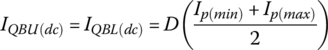
The average currents in the A‐leg switches are
The average currents in the B‐leg switches are
The rms currents in the B‐leg diodes are due to conduction modes II or IV:

The average currents in the B‐leg diodes are

For this CCM mode, the rms and average currents in the A‐leg diodes are both zero.
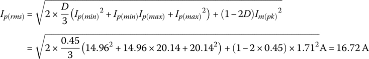
12.3.2.1 Example: Current Ratings in a Medium‐Power Full‐Bridge Converter
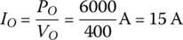
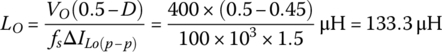
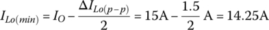
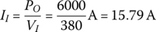
A full‐bridge converter with a high‐voltage full‐bridge rectifier is designed to the following specifications: input voltage of 380 V, output voltage of 400 V, output power of 6 kW, switching frequency of 100 kHz, and a magnetizing inductance of 0.5 mH.
- Size the output inductor to ensure a peak‐to‐peak current ripple ri = 10% at full load.
- Determine the various component currents.
- Determine the AP for the transformer with the following parameters: copper fill factor kcu = 0.5, current density Jcu = 6A/mm2, and maximum core flux density Bmax = 20 mT.
Assume a maximum duty cycle of 0.45 at 400 V output.
Ignore all losses, device voltage drops, and the effects of leakage.
Solution:
- The turns ratio is
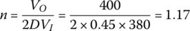
- The dc output current is the output power divided by the output voltage:
- The peak‐to‐peak output inductor ripple current is

- The output inductance is given by rearranging Equation (12.21):
- The dc output current is the output power divided by the output voltage:
- The inductor currents are
- The minimum and maximum secondary currents are given by
- For the full‐bridge rectifier, the secondary current is given by
- The output diode currents are
- The minimum and maximum reflected secondary currents are given by


- The peak value of the magnetizing magnitude is
- Thus, the minimum and maximum primary currents are given by


- The rms of the primary current is
- The currents in the A‐leg switches are
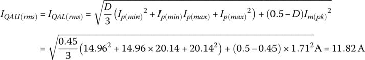
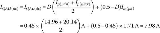
- The currents in the B‐leg switches are
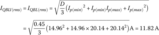
- The currents in the B‐leg diodes are


- We can check this calculation by noting the following: the average input current should equal the sum of the average currents in the A‐ and B‐leg switches minus the B‐leg diode average current. The input current is given by
- Alternatively,

- which confirms the value.
- The minimum and maximum secondary currents are given by
- The transformer AP is given by

- for the full‐bridge rectifier converter
12.3.3 CCM Voltages in the Full‐Bridge Converter
A significant constraining factor for a single‐switch forward is the relatively high voltage across the semiconductor device. The primary‐side switches and diodes in a full‐bridge converter are simply limited to the input voltage plus any overshoot.
In equation form, the maximum voltage across the switch VQ(max) is

where VQ(OS) is the overshoot. Again, it is necessary to derate the semiconductor devices in order to operate the device safely. A reasonable derating is to operate the device at up to 80% of the rated voltage.
The voltage across the output diode should factor in the reflected primary voltage. The maximum voltage across the secondary diode VD(max) is

where VD(OS) is the diode overshoot.
12.3.3.1 Example: Voltage Ratings in a Full‐Bridge Converter
The full‐bridge converter in the previous example has an input voltage of 380 V.
- Determine the maximum voltages seen by the devices. Assume an overshoot of 100 V on the switch and 100 V on the secondary diodes.
- What are reasonable rated voltages for these semiconductor components?
Solution:
- The maximum voltage across the switch is

- The secondary diodes will see a maximum voltage of

- The secondary diodes will see a maximum voltage of
- The minimum rated voltage of the switch is

A rated voltage of 600 V would be appropriate for the primary devices.
The minimum rated voltage of the diode is

Thus, a rated voltage of 700 V, rounded up to the nearest 100 V, would be appropriate for the diode when derated.
12.4 Resonant Power Conversion
Resonant and soft‐switched power converters are commonly used for power conversion. Soft switching is desirable in a power converter as the switching losses of the semiconductors can be significantly reduced, albeit at the expense of circuit complexity and conduction losses. Resonant converters form a class of switch‐mode power converters which enable soft switching by using passive elements such as inductors and capacitors to generate quasi‐sinusoidal currents and voltages within the power circuitry. The quasi‐sinusoidal waveforms typically have a lower high‐frequency content, with reduced harmonics, than the hard‐switched quasi‐linear waveforms which we have observed in the forward and full‐bridge converters investigated in this chapter so far.
Resonant power converters have played a significant role in the development of inductive and wireless charging. There are a number of basic reasons for the special suitability of resonant converters:
- The transformers by their nature are loosely coupled as significant displacements can occur between the primary and secondary windings, resulting in very high leakage inductances and a very low magnetizing inductance [5]. In addition, these inductances can exhibit significant variation during operation due to the alignment of the secondary winding on the vehicle and the off‐vehicle primary winding. The long cables result in additional leakage inductance.
- Operation of the power circuitry should be at as high a frequency as possible in order to minimize the size and mass of the passive components, especially the loosely coupled transformer.
- Circuit waveforms should be as sinusoidal as possible in order to minimize high‐frequency effects which can cause significant heating and excessive EMI. EMI can be a particularly difficult area to address and is a significant consideration when selecting a circuit topology for wireless charging.
A hard‐switched converter requires a low‐leakage transformer in order to function. A resonant converter with a series‐resonant LC circuit can handle the high leakage and low magnetizing inductances. A capacitor can be added in parallel with the low magnetizing inductance to cancel the effects of the low inductance and provide a resonant boost for the converter. The parallel capacitor increases the resonant currents, which has the benefit of enabling soft switching over the entire operating region. While the resonant currents increase, the high gain transformer and capacitor boost help to reduce cable and primary currents and the associated copper losses.
12.4.1 LCLC Series‐Parallel Resonant Converter
The series‐parallel LCLC resonant converter was the technology of choice for the inductive charging system developed in the 1990s (see also Chapter 14). A simplified circuit diagram is as shown in Figure 12.12.
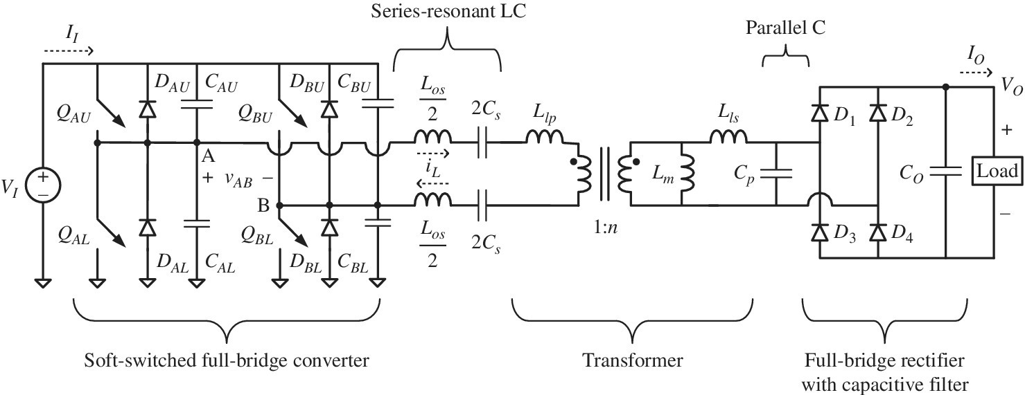
Figure 12.12 Inductive charging resonant topology.
The full‐bridge converter is a variation on the earlier hard‐switched topology. The resonant full bridge has the additional discrete capacitors, CAU, CAL, CBU, and CBL, which are added across the switches and are necessary to enable a zero‐voltage turn‐off of the switch.
The series‐resonant tank components are Los and Cs. These components are shown in the diagram as two series sets. For simplicity, it is assumed that the cable inductance, which can be relatively significant, is integral to the series‐resonant tank inductances. (Splitting the series tank as shown provides equal impedance on each pole output and aids in reducing common‐mode EMI.)
The transformer is presented with explicit primary and secondary leakage inductances, Llp and Lls, magnetizing inductance Lm, and a transformer turns ratio n.
A discrete capacitor Cp is placed on the transformer secondary to create a resonance with the magnetizing inductance of the transformer.
The output rectifier is also a full bridge with diodes D1–D4, and the output is filtered using a capacitive filter.
12.4.2 Desirable Converter Characteristics for Inductive Charging
The following is a list of the general desired converter characteristics for inductive charging [6]:
- Unity transformer turns ratio.
- The ac utility voltage is nominally 230 V for a single‐phase input. The dc link voltage is typically in the 380 V to 400 V range from a boost‐regulated PFC stage. The required battery charging voltage is generally in the 200 to 450 V range. Thus, a transformer turns ratio of unity is desirable to minimize primary‐ and secondary‐side voltage and current stresses.
- Buck/boost voltage gain and current‐source capability.
- Based on Note (1) above, buck/boost operation is required when using a transformer ratio of unity in order to regulate over the full input and output voltage range. A desirable feature of the converter is that it should operate as a controlled current source.
- Capacitive output filter.
- The vehicle inlet should have a capacitive rather than an inductive output filter stage to reduce the on‐vehicle cost and weight, and also desensitize the converter to the operating frequency and power level.
- Monotonic power transfer curve over a wide load range.
- Wide load operation is required for the likely battery voltage range. The output power should be monotonic with the controlling variable over the load range.
- Throttling capability down to no load.
- All battery technologies require a wide charging current range, varying from a rated power charge to a trickle charge for battery equalization, especially at high voltages.
- High‐frequency operation.
- High‐frequency operation is required to minimize vehicle inlet weight and cost and the general size of the passive components.
- Full‐load operation at minimum frequency for variable frequency control.
- Optimizing transformer operation over the load range suggests that full‐load operation takes place at low frequencies.
- Narrow frequency range.
- The charger should operate over as narrow a frequency range as possible for two principal reasons. First, the passive components can be optimized for a given range, and second, operation into the AM radio band is avoided as electromagnetic emissions in this region must be even more tightly controlled.
- Soft switching.
- Soft switching of the converter stage is required to minimize semiconductor switching loss for high‐frequency operation. Zero‐voltage‐switching of a power MOSFET with its slow integral diode can result in high efficiency and cost advantages. Similarly, soft recovery of the output rectifiers results in reduced power loss and a reduction in EMI.
- High Efficiency.
- The power transfer must be highly efficient to minimize heat loss and to maximize the overall fuel economy of the electric vehicle charging and driving cycle.
- Secondary dv/dt control.
- Relatively slow dv/dt’s on the cable and secondary result in reduced high‐frequency harmonics and less parasitic ringing in the cable and secondary, minimizing electromagnetic emissions.
- CCM quasi‐sinusoidal current waveforms.
- Quasi‐sinusoidal current waveforms over the load range result in reduced high‐frequency harmonics and less parasitic ringing in the cable and secondary, minimizing electromagnetic emissions.
12.4.2.1 Basic Converter Operation
The full bridge operates as a square wave voltage generator vAB, as shown in Figure 12.13(a). A quasi‐sinusoidal current iser flows from the full bridge into the series components. The current has the general form as shown in Figure 12.13(a).
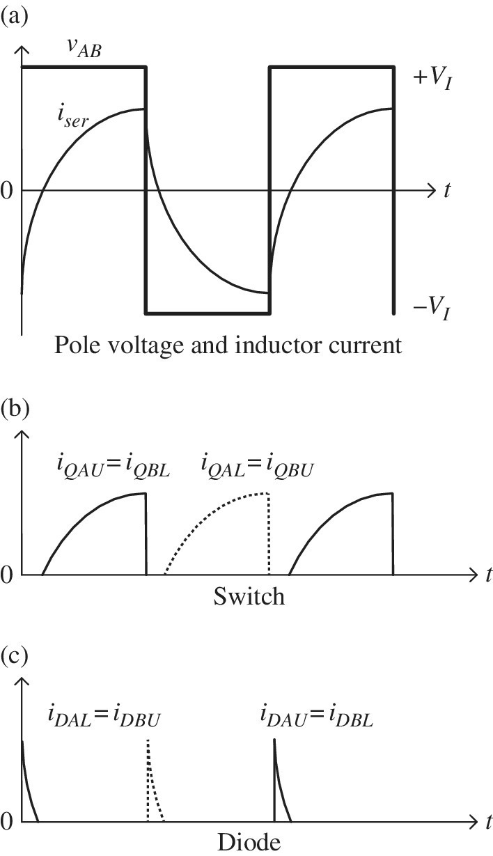
Figure 12.13 Pole voltage and inductor, switch, and diode currents.
The conduction of the various full‐bridge devices are shown in Figure 12.13(b) and (c) for the switches and diodes, respectively. As can be seen, the switches turn on at zero current while the diodes turn off at zero current – avoiding diode reverse‐recovery loss. The switches turn off and the diodes turn on at a finite current. However, the switches do not experience a turn‐off loss as the additional discrete capacitors absorb the inductor current and enable a low‐loss turn‐off of the switch.
The sequence for the zero‐voltage switching (ZVS) turn‐off is as shown in Figure 12.14. Initially, the upper switch QU is conducting, as shown in Figure 12.14(a). The switch is rapidly turned off, and the inductor current rapidly transitions to the two capacitors, thus maintaining the switch voltage low while it turns off. The capacitors CU and CL charge and discharge, respectively, with time until the lower diode DL is forward‐biased and conducts the inductor current.
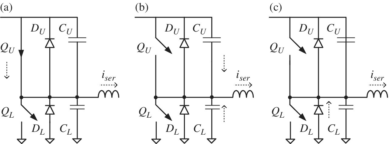
Figure 12.14 ZVS turn‐off of the switch.
The inductor current flows into the cable and into the primary of the coupling transformer. A portion of the current charges and discharges the parallel capacitor, with the balance of the current flowing into the output filter capacitor when the diodes conduct.
The resonant converter of Figure 12.12 can be simplified to the more basic diagram of Figure 12.15, where the inverting full bridge is represented by a simple square wave. The secondary components are shown reflected to the primary. Variables iR and vR represent the current into and the voltage across the rectifier.
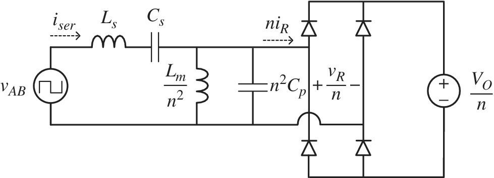
Figure 12.15 Simplified equivalent circuit.
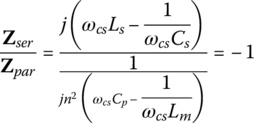
In this circuit, the equivalent series tank inductance Ls is given by
12.4.2.2 Design Considerations
There are a number of design considerations in selecting the various components.
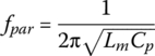
The natural frequency of the series‐resonant tank is given by
The natural frequency of the parallel resonant tank is given by
The following two considerations apply:
- The natural frequency of the parallel resonant tank should be less than the minimum switching frequency fs(min) in order to ensure a voltage gain for the power converter.
- The natural frequency of the equivalent series‐resonant tank should be less than the minimum switching frequency and less than the natural frequency of the parallel resonant tank in order to ensure a zero‐current turn‐on of the switch.
Thus:

12.4.3 Fundamental‐Mode Analysis and Current‐Source Operation
Analysis of the LCLC converter can be quite complex [6, 7]. A simplified analysis, known as fundamental‐mode analysis, can be used to explore the operation of the circuit at the switching or fundamental frequency [7]. The analysis is based on phasors rather than on time‐domain analysis. In terms of phasors, let the impedances of the series and parallel tanks be
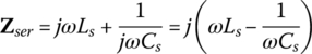
and
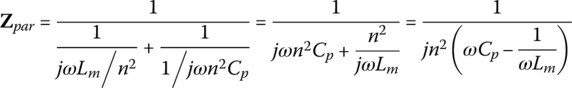
where ω is the switching frequency, and j is the imaginary operator.
A key characteristic of the series‐parallel resonant converter is current‐source operation. Current‐source operation can be explained using the analysis in this section. First, Figure 12.15 is redrawn to represent the rectifier and output as an equivalent voltage source vR as shown in Figure 12.16.
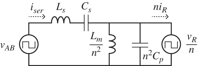
Figure 12.16 Simplified equivalent circuit.
The circuit can then be redrawn as the simple circuit shown in Figure 12.17. The use of boldface emphasizes that the variable is a phasor with a magnitude and phase.
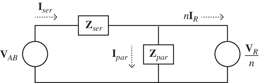
Figure 12.17 Equivalent circuit at fundamental frequency.
From Kirchhoff’s voltage law:
which can be expressed in terms of the parallel and rectifier currents as
since

But

Substituting Equation (12.54) into Equation (12.52) gives
At the current‐source frequency ωcs, the following condition holds:

At this frequency, the rectifier current is only a function of the input voltage and the series tank impedance:

and is independent of the magnitude of the output voltage. Thus, the circuit acts as a current source.
The current‐source frequency is determined by solving
which is the solution of a quadratic equation.
However, we now take a shortcut and estimate an approximate current‐source frequency by assuming that the series inductance and parallel capacitance are the significant components at the current‐source frequency. Thus:
which results in the following simple solution for the current‐source frequency:
and
We can estimate the output current at the current‐source frequency by making some further simplifying assumptions.
First, we assume that the full‐bridge inverter voltage vAB can be represented by the rms value of the fundamental frequency of the square wave of magnitude VI, as shown in Figure 12.18(a).
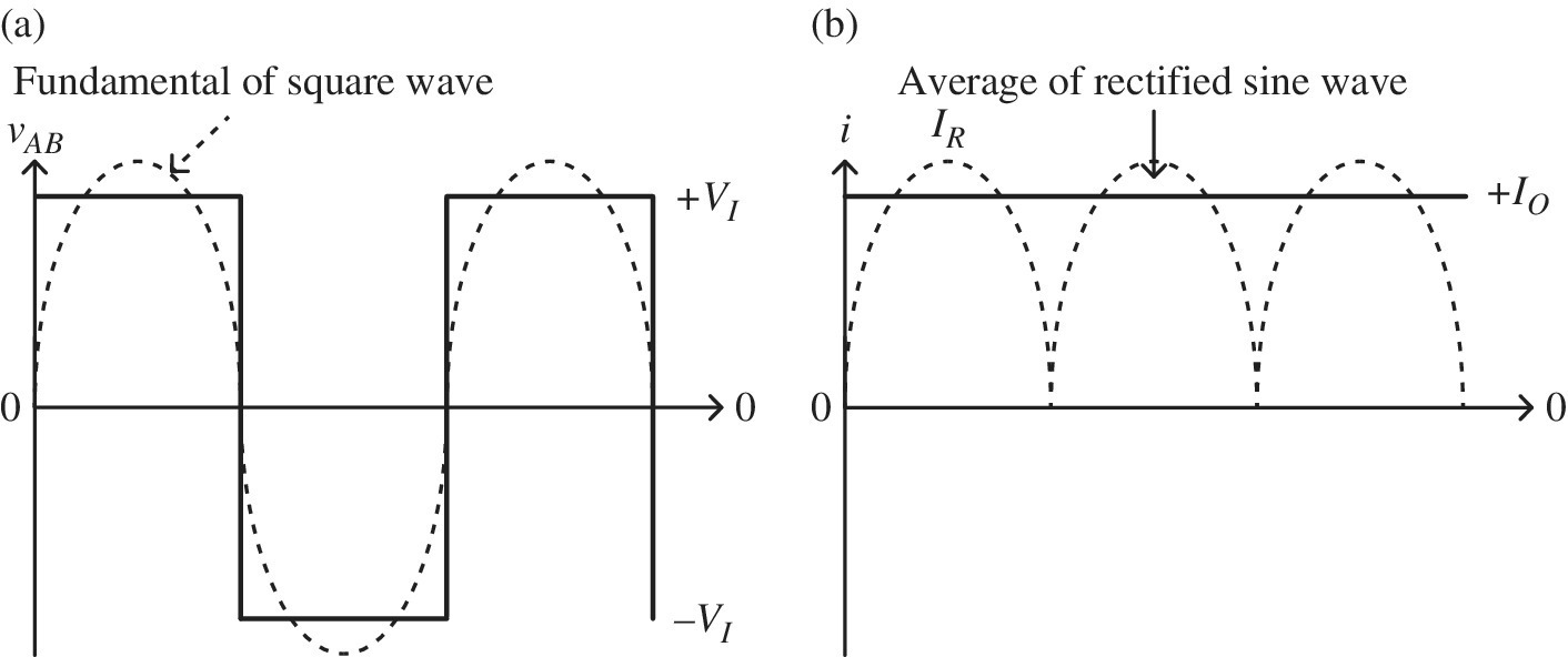
Figure 12.18 Simplified inverter and rectifier waveforms.
Using Fourier analysis, it can be shown that the relationship between the rms value of the fundamental VAB(rms) and the square wave of magnitude VI is given by
Second, we assume that the value of the output current IO is the average of a rectified sine wave of rms value IR(rms), as shown in Figure 12.18(b), and is simply related by
Substituting Equation (12.62) and Equation (12.63) into Equation (12.57) enables us to derive a relationship between the dc input voltage and the dc output current at the current‐source frequency. Therefore:
Thus:
Note that the magnitude of the series impedance at a particular frequency is given by
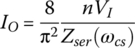
12.4.3.1 Example
The following specifications are representative values for the SAE J1773 inductive charging standard: Lm = 45 μH, Cp = 40 nF, Los = 17 μH, Llp = Lls = 1 μH, Cs = 0.33 μF, and n = 1.
Determine the series, parallel, and current‐source frequencies.
Determine the approximate output current and output power at the current‐source frequency when VI = 380 V and VO = 400 V.
Solution:
The equivalent series inductance is


The magnitude of the series impedance at the current‐source frequency is given by
Thus, the dc output current is
and the output power is

12.4.4 Simulation
The analytical modeling of the LCLC topology can be complex [1–7]. The converter can be modeled using any circuit simulator. A simplified Simulink circuit model is as shown in Figure 12.19.
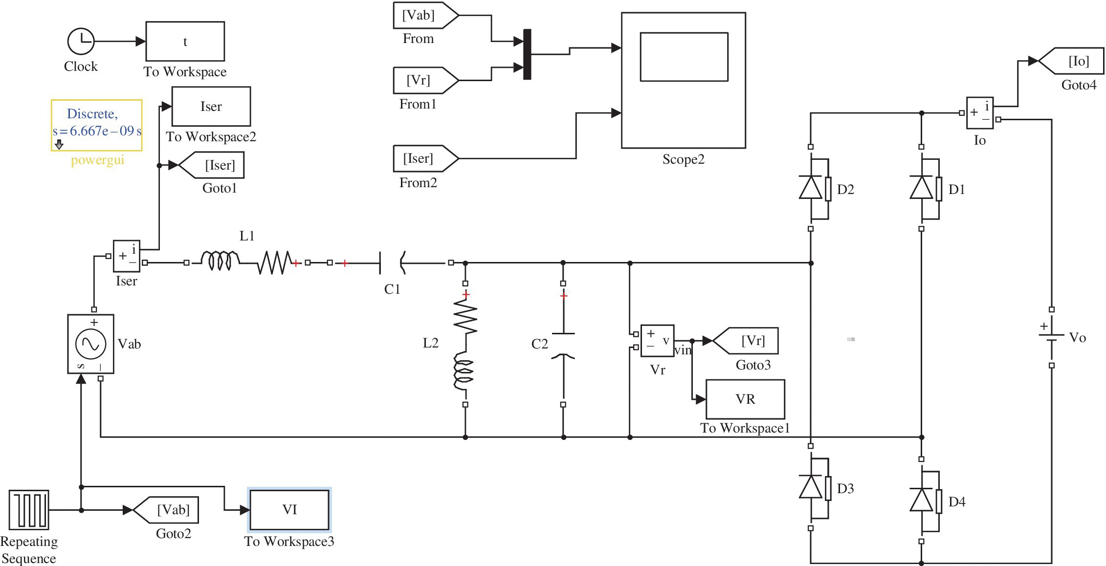
Figure 12.19 Simple Simulink LCLC circuit model
The circuits waveforms for the input and rectifier voltages and the series tank current are presented in Figure 12.20.
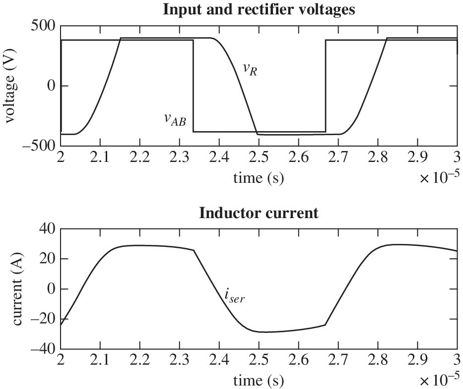
Figure 12.20 Simple LCLC circuit model current waveforms.
The circuit is simulated for a dc link voltage of 380 V and two output voltages of 200 V and 400 V. The results of the simulation versus frequency are presented in Figure 12.21 for (a) 200 V and (b) 400 V. The output current, and the resulting power, can be controlled by increasing or decreasing the switching frequency. The series inductor current remains high even when the output current is low. Maintaining the series tank current high is necessary in order to ensure ZVS of the switches.
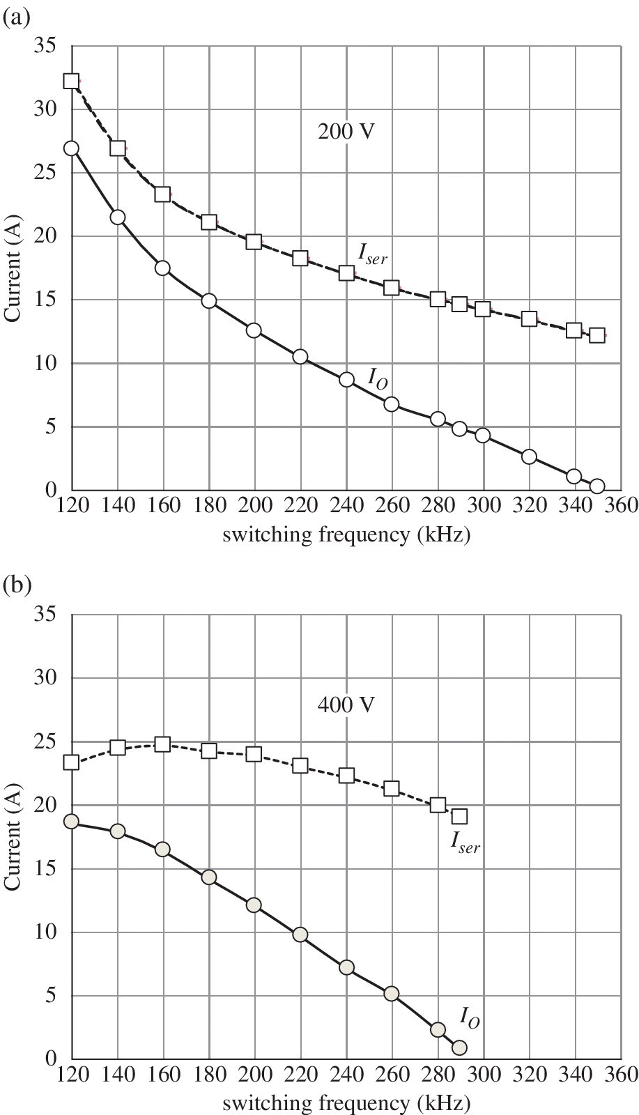
Figure 12.21 Rms series inductor current and dc output current at output voltages of (a) 200 V and (b) 400 V.
References
- 1 J. G. Hayes, Resonant Power Conversion Topologies for Inductive Charging of Electric Vehicle Batteries, PhD Thesis, University College Cork, 1998.
- 2 R. Severns, E. Yeow, G. Woody, J. Hall, and J. G. Hayes, “An ultra‐compact transformer for a 100 W to 120 kW inductive coupler for electric vehicle battery charging,” IEEE Applied Power Electronics Conference, pp. 32–38, 1996.
- 3 J. M. Leisten, “LLC design for UCC29950,” Texas Instruments application note, 2015.
- 4 TI staff, “Phase‐shifted full bridge dc/dc power converter design guide,” Texas Instruments application note, 2014.
- 5 J. G. Hayes, N. O'Donovan, and M. G. Egan, “Inductance characterization of high‐leakage transformers,” IEEE Applied Power Electronics Conference, pp. 1150–1156, 2003.
- 6 J. G. Hayes, M. G. Egan, J. M. D. Murphy, S. E. Schulz, and J. T. Hall, “Wide load resonant converter supplying the SAE J‐1773 electric vehicle inductive charging interface,” IEEE Transactions on Industry Applications, pp. 884–895, July–August 1999.
- 7 J. G. Hayes and M. G. Egan, “Rectifier‐compensated fundamental mode approximation analysis of the series‐parallel LCLC family of resonant converters with capacitive output filter and voltage‐source load,” IEEE Power Electronics Specialists Conference, pp. 1030–1036, 1999.
Further Reading
- 1 N. Mohan, T. M. Undeland, and W. P. Robbins, Power Electronics Converters, Applications and Design, 3rd edition, John Wiley & Sons, 2003.
- 2 N. Mohan, Power Electronics: A First Course, John Wiley & Sons, 2012.
- 3 R. W. Erickson, Fundamentals of Power Electronics, Kluwer Academic Publishers, 2000.
- 4 R. E. Tarter, Principles of Solid‐State Power Conversion, SAMS, 1985.
- 5 J. G. Hayes and M. G. Egan, “A comparative study of phase‐shift, frequency, and hybrid control of the series resonant converter supplying the electric vehicle inductive charging interface,” IEEE Applied Power Electronics Conference, pp. 450–457, 1999.
- 6 M. G. Egan, D. O’Sullivan, J. G. Hayes, M. Willers, and C. P. Henze, “Power‐factor‐corrected single‐stage inductive charger for electric‐vehicle batteries,” IEEE Transactions on Industrial Electronics, 54 (2), pp. 1217–1226, April 2007.
- 7 R. Radys, J. Hall, J. Hayes, and G. Skutt, “Optimizing AC and DC winding losses in ultra‐compact high‐frequency power transformers,” IEEE Applied Power Electronics Conference, pp. 1188–1195, 1999.
Problems
- 12.1 Determine the rms component of the various currents for Example 12.2.1.1 when the input voltage increases to 400 V. [Ans. ILo(rms) = 15.01 A, Is(rms) = ID2(rms) = 7.51 A, ID1(rms) = 13 A, Ip(rms) = IQ(rms) =1.031 A, IT(rms) = 0.144 A]
- 12.2 A single‐switch forward converter is designed to the following specifications: input voltage of 42 V, output voltage of 12 V, output power of 240 W, switching frequency of 200 kHz, and a magnetizing inductance of 500 μH.
- Size the output inductor for a peak‐to‐peak current ripple of 10% at full load.
- Determine the various component currents at full load.
- Determine reasonable rated voltages, rounded up to the nearest 10 V, for the switch and output diodes if the input voltage can go as high as 60 V. Allow for overshoots of 10 V on both the switch and diodes.
- Determine the AP for the transformer. Let copper fill factor k = 0.5, current density Jcu = 6A/mm2, and maximum core flux density Bmax = 20 mT.
Ignore all losses, device voltage drops, and the effects of leakage.
[Ans. Io(dc) = 20 A ILo(rms) = 20.01 A, Is(rms) = ID2(rms) = 14.15 A, ID2(dc) = 10 A, ID1(rms) = 14.15 A, ID1(dc) = 10 A, Ip(rms) = IQ(rms) =8.16 A, IT(rms) = 0.086 A, 170 V, 60 V, AP = 1.42 cm4]
- 12.3 Determine the various primary‐side currents for the full‐bridge converter of Example 12.3.2.1 when the battery voltage decreases to 200 V. [Ans: Ip(rms) = 23.58 A, IQA(rms) = 16.68 A, IQA(dc) =8.13; A, IQB(rms) = 16.67 A, IQB(dc) = 7.89 A, IDB(dc) = 0.24 A]
- 12.4 Recalculate the various currents for the full‐bridge Example 12.3.2.1, but simplify the analysis by assuming that the magnetizing current is negligible and can be ignored. [Ans: Io(dc) = 15 A, ILo(rms) = 15.01 A, IDo(rms) = 10.34 A, IDo(dc) = 7.5 A, Ip(rms) = 16.65 A, IQA(rms) = 11.77 A, IQA(dc) = 7.89 A, IQB(rms) = 11.77 A, IQB(dc) = 7.89 A, IDB(dc) = 0 A]
- 12.5 A full‐bridge converter with a center‐tapped rectifier is designed to the following specifications: input voltage of 380 V, output voltage of 15 V, output power of 2.4 kW, switching frequency of 100 kHz, and a magnetizing inductance of 1 mH.
- Size the output inductor for a peak‐to‐peak current ripple of 10% at full load.
- Determine the primary and secondary rms currents at full load.
- Determine the AP for the transformer. Let the copper fill factor k = 0.5, current density Jcu = 6A/mm2, and maximum core flux density Bmax = 20 mT.
Ignore all losses, device voltage drops, and the effects of leakage.
Note that, as there are two identical secondaries, the AP is given by
[Ans. Lo = 0.4688 μH, Is(rms) = 110.3 A, Ip(rms) = 6.7 A, AP = 23.3 cm4]
- 12.6 Determine the currents for the preceding problem when the output voltage decreases to 12 V. [Ans: Is(rms) = 131.3 A, Ip(rms) = 7.49 A]
- 12.7 For the LCLC converter of Section 12.4.3.1, determine the approximate output current and output power at the current‐source frequency when the input voltage is 200 V and the output voltage is 400 V. [Ans. 8.47 A, 3.39 kW]
Assignments
- 12.1 Verify the waveforms and answers for the various examples and problems using a circuit simulator of your choice.
Appendix I: RMS and Average Values of Ramp and Step Waveforms
It can easily be shown that the rms and average values of a periodic discontinuous ramp waveform are given by
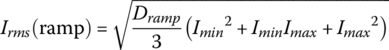
and
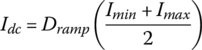
where Imin and Imax are the minimum and maximum currents, respectively, and Dramp is the duty cycle of the ramp. These equations can be applied to all the current waveforms in Figure 12.6(b)–(g).
Similarly, the rms and average values of a periodic discontinuous step waveform are given by

and

where Istep is the amplitude of the step current, and Dstep is the duty cycle of the step.
If the waveform features a combination of discontinuous periodic ramps, as in Figure 12.10(b) and (c), then the rms and average of the waveforms are
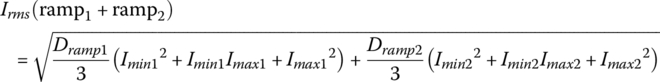
and

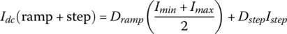
If the waveform features a combination of a discontinuous periodic ramp and a step, as in Figure 12.10(f), (g), and (k), then the rms and average of the waveforms are

and
Appendix II: Flyback Converter
The transformer‐coupled buck‐boost converter is known as the flyback converter and is the commonly used switch‐mode power converter for low‐power applications. A simplified flyback converter is shown in Figure 12.22. The transformer acts to store energy in the primary winding and then release the energy to the secondary. Note that when the primary is energized, there is no secondary current, and vice versa. The inductive operation can be viewed as representing coupled‐inductor action rather than transformer action.
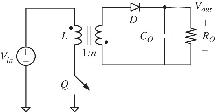
Figure 12.22 Flyback converter.
The CCM duty cycle for the buck‐boost converter is given by
and the voltage gain is given by