14
Battery Charging
“Power can be, and at no distant date will be, transmitted without wires, for all commercial uses, such as the lighting of homes and the driving of aeroplanes. I have discovered the essential principles, and it only remains to develop them commercially. When this is done, you will be able to go anywhere in the world — to the mountain top overlooking your farm, to the arctic, or to the desert — and set up a little equipment that will give you heat to cook with, and light to read by. This equipment will be carried in a satchel not as big as the ordinary suit case. In years to come wireless lights will be as common on the farms as ordinary electric lights are nowadays in our cities.”
Nikola Tesla (1856–1943)
In this chapter, we investigate the charging of electric vehicles from the electric grid. Battery charging connects the vehicle to the electric grid, and many factors must be considered, such as available voltages and wiring, standardization, safety, communication, ergonomics, and more. Various charging architectures and charging standards are used. Conductive and wireless standards are discussed. The boost power‐factor correction power stage is investigated in detail.
14.1 Basic Requirements for Charging System
Many important issues must be considered when selecting the charging system. The principal issues are safety, reliability, user‐friendliness, power levels and charging times, communications, and standardization. These issues are briefly discussed as follows.
- Safety: This is the most serious consideration for any automotive manufacturer introducing an electric vehicle (EV) to the consumer marketplace. The battery charger system must minimize the risk of electrical shock, fire, and injury to the end user for a wide range of operating and fault conditions. The system must provide various levels of insulation and safety checks in order to ensure a safe system. There are a number of electrical safety standards which are used around the world. The principal standards are from Underwriters Laboratories (UL) in the United States and VDE in Germany. It is necessary to obtain safety approvals from these types of agencies in order to sell products in many countries.
- Reliability: The automotive environment is very harsh. The same performance is expected whether a car is driven in the dry heat of the Arizona desert, the freezing cold of Minnesota, or the humid conditions of Florida. The car is exposed to significant shock and vibration in addition to corrosive solvents, salt, water, and mud. The charger for the EV must have a long service life with daily operation. The electrical connector must be designed to withstand over 10,000 insertions and withdrawals in these harsh conditions and still remain safe for the consumer for the many fault scenarios. For example, the plug and cable should be able to withstand the vehicle weight in case the vehicle accidentally drives over the assembly.
- User‐friendliness: A consumer product such as a car requires that significant attention be paid to customer expectations and ergonomics. The present method of fueling a vehicle with an internal combustion engine is simple and straightforward. EV charging must also be simple and should pose minimal challenge to EV users or to young children whom a parent may send to “plug in the car.” Greater emphasis has to be placed on the ergonomics of refueling an EV compared to a gasoline‐fueled car. The basic reason for this is that the EV may require daily charging, whereas the gasoline‐powered car may only be fueled once a week or less. Such ergonomic considerations as single‐handed operation and intuitive insertion and withdrawal processes help the user.
- Power levels and charging times: The charging time for an EV can range from tens of minutes, if high‐power charging is used, to many hours, if low‐power chargers are used. Thus, for EVs to gain widespread acceptance, the charging power levels should be maximized in order to reduce the charging times. However, in practice the power levels can be limited by the household electrical wiring, electrical grid impacts, battery chemistries and degradation due to high charging levels, and, of course, size and cost. Given the importance of optimizing society’s use of energy, it is important to charge efficiently. However, as, discussed in Chapter 3, battery charging efficiency can drop with higher power levels.
- Communication: At a basic level, the plug and cable assembly must not only transmit power, but must also provide a communications path between the charger and the vehicle in order to ensure a safe and optimized power flow. Communication has taken on a greater role in society in the twenty‐first century as smartphones and the Internet are part of the overall communications and control interfaces. Simple messages relating to availability, maximum power output, charging time, and problem or fault reporting are also critical communications.
- Standardization: Market acceptance of a new product can be accelerated by creating a product standard. A market standard can reduce the cost by ensuring a larger market with access to more charging points and ease of communication. An advantage of a commonly agreed standard is that the automotive companies do not have to compete on the charging but can focus on the vehicle.
- Compliance: Many regulations already exist to ensure safe and reliable operation of electrical equipment. The equipment must also comply with standards to limit electrical noise emissions, commonly known as electromagnetic interference (EMI), an area of government regulations in order to protect other electrical devices, for example, cardiac pacemakers, and to limit susceptibility and increase immunity to unwanted emissions from other equipment or from events, such as lightning strikes. Charging systems must comply with all these regulations.
14.2 Charger Architectures
Before the various charging topics are investigated in more depth, it is useful to consider the basic electrical power conversions required to charge a battery.
A basic block diagram of the charging power flow is shown in Figure 14.1. A wonder of the modern world is the electrical grid. The electrical grid provides alternating current (ac) voltages and currents at an electrical frequency. Voltages and frequencies vary around the globe and will be discussed in the next section. The ac supply frequency is low and is typically 50 Hz or 60 Hz. A battery requires direct current (dc) electricity, and so the first stage of the power conversion is to rectify and filter the ac waveform from the grid to dc. However, this first‐stage conversion to dc cannot be supplied directly to the battery, as a transformer is typically required to order to provide electrical safety to the user. Thus, the dc is chopped to create a stream of very high‐frequency ac (hfac) waveforms. Frequencies of tens or hundreds of kilohertz are common to minimize transformer size. A transformer is used to provide a physical barrier in the electrical path between the ac grid and the battery and to minimize failure modes which could result in life‐threatening mishaps. The high‐frequency ac is rectified and filtered to create dc to supply the battery.
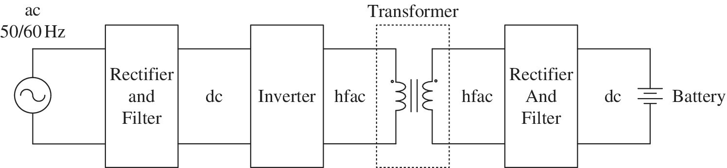
Figure 14.1 Basic power block diagram for battery charging.
There are a number of options for charging the vehicle, and there are a variety of charging technologies available for EVs. Choices and decisions must be made by the various manufacturers, infrastructure providers, and the consumers with respect to the following areas: conductive or wireless/inductive charging, high‐power or rapid charging, on‐board versus off‐board chargers, and integral charging.
Conductive charging is the common approach to charging a vehicle. Conductive charging simply means that the vehicle is electrically connected to the off‐board powering system by a conductive plug and socket assembly, similar to the operation of common household electrical appliances. Generally, vehicles feature a low‐to‐medium power on‐board charger, with ac being supplied from the electrical grid to the vehicle. Figure 14.1 is modified to that shown in Figure 14.2 to include all the charging components on the vehicle.
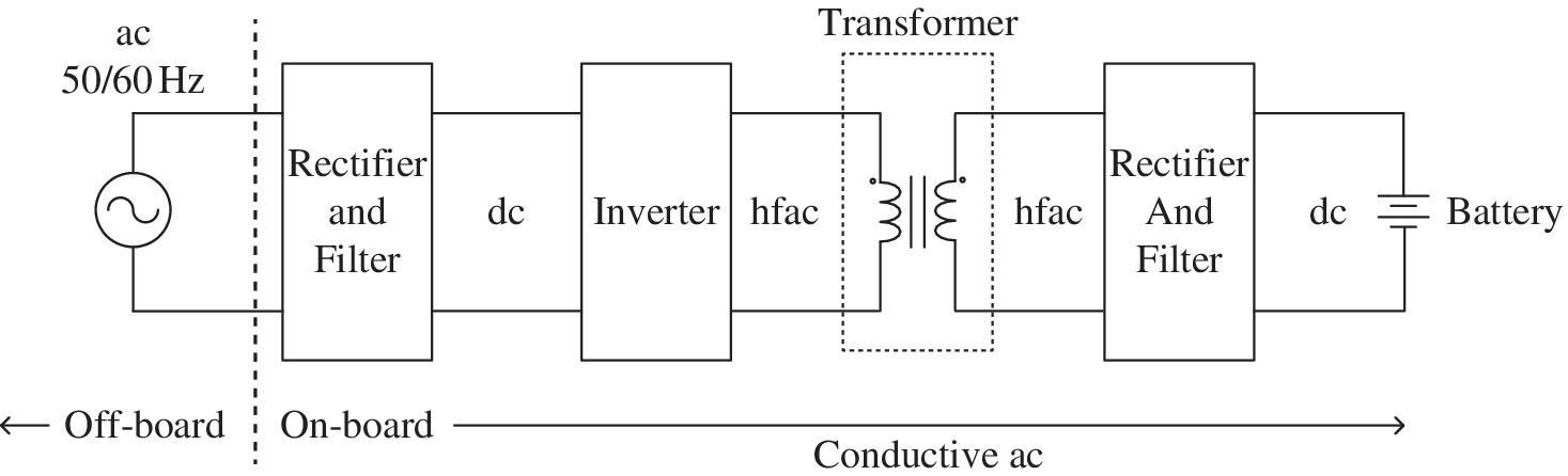
Figure 14.2 Conductive ac charging power block diagram.
While low‐to‐medium power chargers are expected to be the commonly used charging approach, an enabler for EVs is the capability to rapidly charge using a high‐power charger. High‐power chargers can be very large physically and are designed as stationary off‐board devices to be operated in a similar manner to a gasoline pump at a filling station. In this case, the charger is off‐board, and dc is supplied on‐board. The conductive dc block diagram is shown in Figure 14.3.
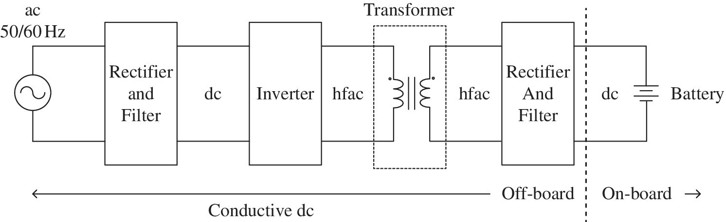
Figure 14.3 Conductive dc charging power block diagram.
Wireless or inductive charging does not connect the vehicle to the electrical grid by a conductive coupling using copper wires. Instead, the magic of transformer coupling is used to couple power from the grid to the vehicle without conductive contacts. Such an approach can result in safety enhancements and consumer ease of use, but also comes with significant engineering challenges. For wireless charging, the partition between the on‐board and off‐board components of the charging system is within the transformer itself, as shown in Figure 14.4.
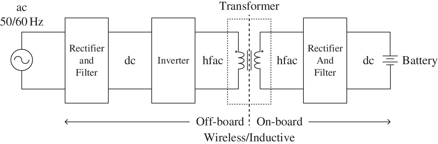
Figure 14.4 Wireless/inductive ac charging power block diagram.
Integral charging was originally employed for the prototype predecessor of the GM EV1, known as the GM Impact, and the technology has since been developed and used by such companies as AC Propulsion and Renault. As shown in Figure 14.5, the technology reconfigures the traction power electronics and machine to re‐employ the components to also perform the power conversions required for charging. Such an approach reduces the overall parts count on the vehicle while requiring additional measures on electrical safety and isolation.
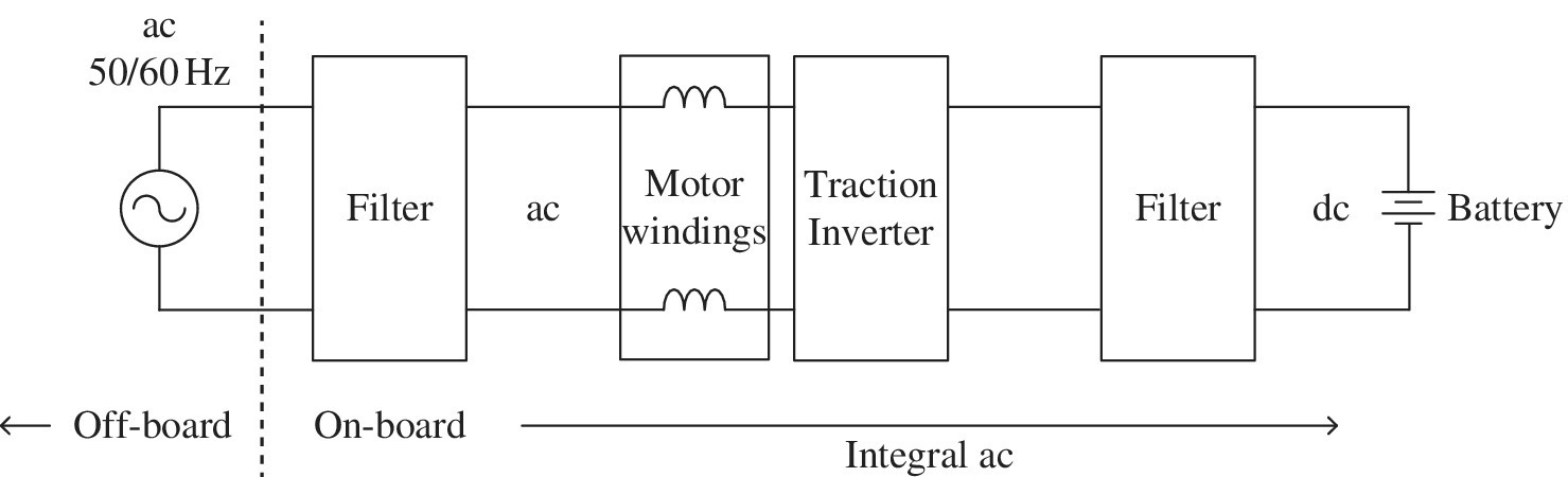
Figure 14.5 Integral ac charging power block diagram.
A significant advantage of the integral charging approach is that the power flow can be made bidirectional. Thus, the vehicle can supply power back to the local grid if required – such operation is known as vehicle to grid (V2G).
Microgrid operation is also possible. A microgrid is a term for a local power grid which can be connected to the main grid, or can be disconnected from the main grid for independent operation if required.
14.3 Grid Voltages, Frequencies, and Wiring
Electrical equipment, especially mobile devices, are designed to operate globally. There are many configurations of wiring and voltage, power, and frequency around the world. This section briefly considers the principal configurations.
First, the world is divided in terms of the electrical frequency of operation. Most countries, with a handful of exceptions, operate at either 50 Hz or 60 Hz. Japan is the notable exception as it has two separate grids, one with 50 Hz to the east and one with 60 Hz to the west. The simplest broad classifications would be that the world operates at 50 Hz except for North and Central America, many countries in South America, South Korea, Saudi Arabia, and a handful of other countries.
Similarly, the world generally operates with a standard voltage of 230 V (in the nominal range of 220–240 V), except for North and Central America, where 120 V is standard, and South Korea and Japan with 100 V.
Note that there can be significant variations in the voltage during regular operation. Equipment working off the standard 230 V would likely be designed to operate off a voltage range of 180 V to 270 V. Equipment can also be designed for universal operation, in which case the input stage is designed to accept a voltage range of 80 V to 270 V. Note that the voltages just discussed are all root‐mean‐squared (rms) values.
The basic residential wiring system provides a phase voltage of 230 V, 50 Hz between the line and neutral, as shown in Figure 14.6(a). The neutral is typically grounded by physically connecting the neutral to a copper grounding rod which is driven into the ground at a location close to the residence. The three wires of line, neutral, and ground are hard‐wired into the charging assembly.
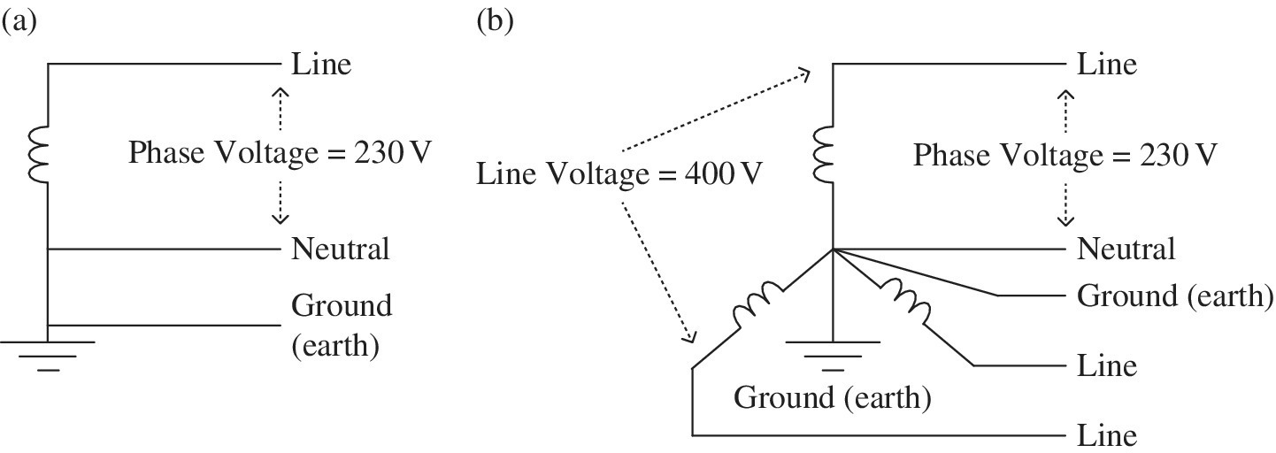
Figure 14.6 Basic 230 V wiring system.
The single‐phase connection is typically provided by a three‐phase transformer. Commercial premises often have a three‐phase connection in order to power electric motors, fans, compressors, and so on. The typical three‐phase configuration is shown in Figure 14.6(b). Three phase can be an option for many charger power levels, in which case the five wires of the three lines, neutral, and ground are supplied to the charging equipment. Simply multiply the phase voltage by  in order to get the appropriate line voltage. Thus, 400 V is the line voltage when the phase‐to‐neutral voltage is 230 V.
It is common in the 60 Hz regions for 100/120 V to be available. Again, basic household wiring provides a single‐phase connection, as shown by Figure 14.7(a). As the 120 V system outputs a relatively low power, it is usual to have a higher voltage available. It is common to have the grounded midpoint single‐phase wiring system of Figure 14.7(b), from which two 120 V outputs are available. Note that these outputs are 180° out of phase with each other, which means that the sum of the two outputs is 240 V, the high‐voltage output.
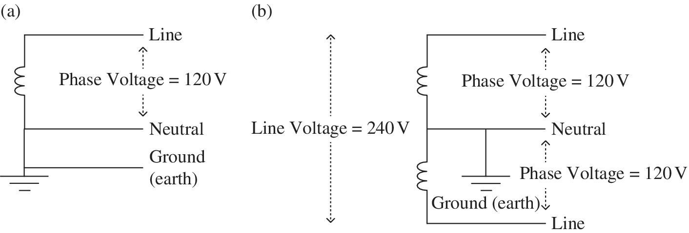
Figure 14.7 Basic 100/120 V wiring system.
The 120 V output, shown in Figure 14.7(a), may itself be the output of a three‐phase transformer with a nominal 208 V line voltage, as shown in Figure 14.8.
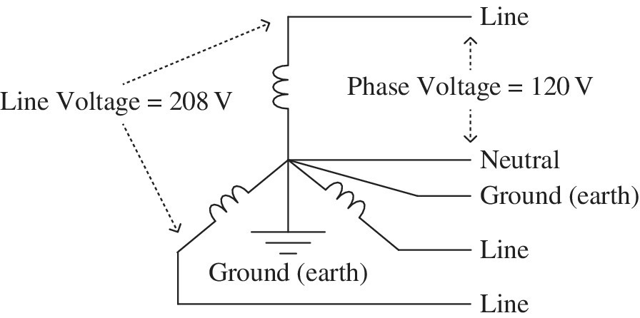
Figure 14.8 Three‐phase 208 V system.
The 240 V winding of Figure 14.7(b) can be the output of a single‐phase winding of a three‐phase star or delta transformer.
The voltages mentioned so far in this section are the typical voltages considered for household and commercial premises. Higher voltages are likely to be used for high‐power charging. These again are three phase, and the wiring configurations can be in star or delta and may feature auxiliary windings.
14.4 Charger Functions
EV chargers are similar in operation but have some key differences compared to battery chargers used in other applications, such as mobile phones and laptop computers. The basic functions of a low‐power battery charger are shown in Figure 14.9. First, we will review the functions of the more basic charger and then turn to the functions of the automotive charger. The related voltage and current waveforms are shown in Figure 14.10. The basic charger power blocks are as follows.
- Ac‐dc rectifier: The function of the ac‐dc rectifier is to rectify, or make positive, the input ac voltage vac and current iac when they are in the negative half cycle. Thus, the output of the diode rectifier is always positive, as can be seen in the waveforms of the rectifier output voltage │vac│ and current │ iac│.
- Dc capacitor: The dc capacitor is charged to the peak ac voltage when the rectified voltage │vac│ exceeds the capacitor voltage. This only happens during a portion of the cycle, and there is a surge of current from the ac input through the diodes and into the capacitor. Thus, the current waveform has a sharp pulsed waveform.
- Dc‐dc converter: The dc‐dc converter converts the high voltage on the dc capacitor to a safe lower voltage for input to the laptop or mobile phone for use in charging. The simplest and most cost‐effective dc‐dc is the switch‐mode flyback converter, which switches at a high frequency and has the transformer isolation that is essential for safety.
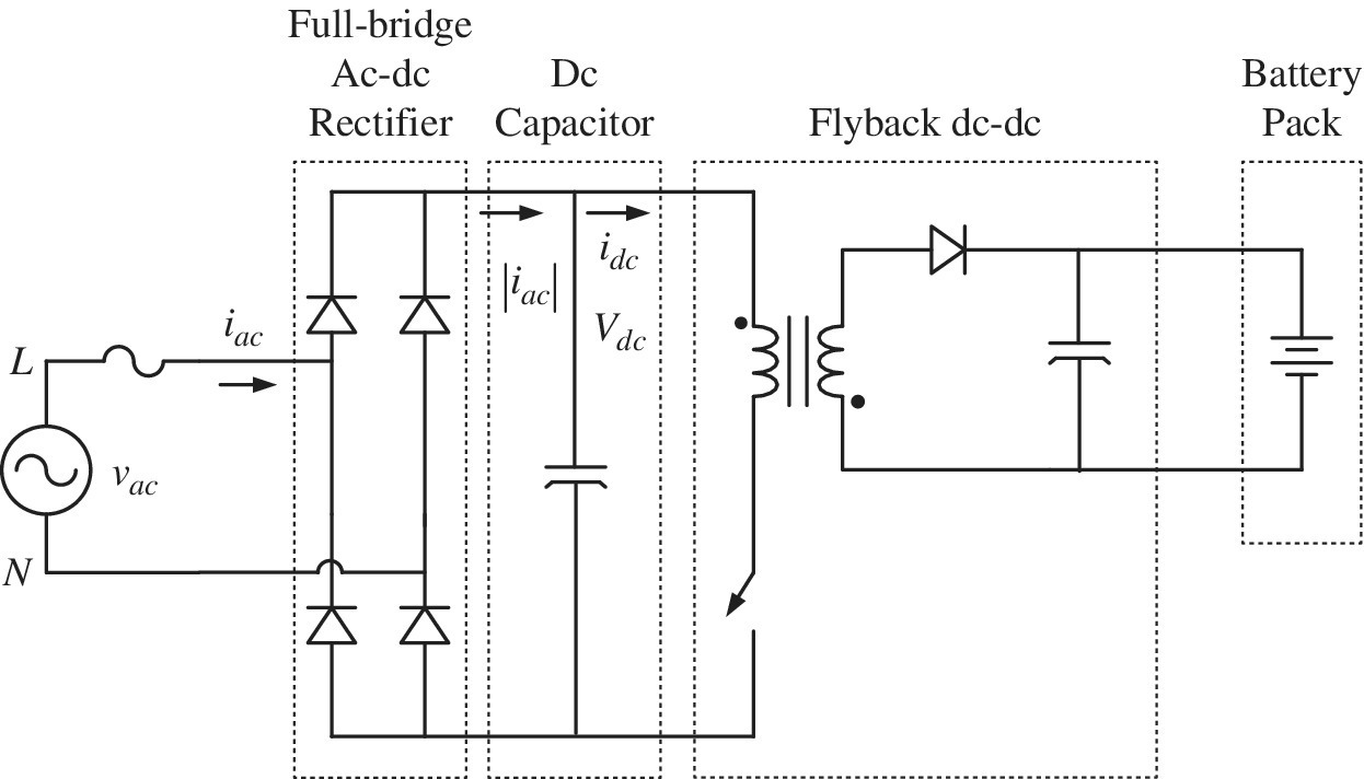
Figure 14.9 Low‐power charger.
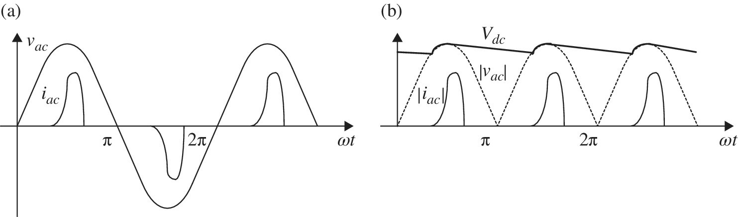
Figure 14.10 (a) Input and (b) rectifier‐capacitor waveforms.
At this point it is useful to identify some very commonly used power terms.
14.4.1 Real Power, Apparent Power, and Power Factor
The apparent power S is the product of the rms voltage V and the rms current I. This product is also known as the volt‐ampere product. In equation form:

The apparent power has the units of volt‐amperes (symbol VA).
The real power P is the true power delivered to an electrical circuit. The real power is the power measured by a wattmeter and has the units of watts (symbol W).
In a power circuit, the apparent power can vary significantly from the real power due to the distortion introduced by the power‐stage components, such as the diode‐capacitive rectifier above, or by the load itself.
The power factor PF is the ratio of the real power to the apparent power:
The power factor is a dimensionless quantity and has no units. A low power factor is undesirable for a number of reasons.
First, a poor power factor results in an increased current for a given voltage in order to supply the required power. From a charging perspective, a low power factor means that maximum power cannot be sourced from the supply even though the maximum current is being supplied.
Second, the diode‐capacitor front‐end, described earlier, results in high‐frequency harmonics of the fundamental 50 or 60 Hz waveform. These harmonics create increased power losses through the distribution system, increasing conductor and transformer temperatures and reducing the efficiency and system reliability.
Third, the current distortion results in voltage distortion of the supply voltage, which affects the supply and the other loads fed from the supply.
Fourth, commercial and industrial customers of the power utilities can be financially penalized for demanding currents with a low power factor.
Global standards have been developed to govern power quality and harmonic distortion. IEC 61000 contains commonly referenced standards addressing harmonics, EMI, and other grid‐related issues.
Thus, simple diode–rectifier–capacitor front‐ends are only permitted in low‐power applications. At levels above hundreds of watts, the simple capacitive filter is buffered with another switch‐mode power converter, known as the boost converter. The boost converter serves to maintain the input current waveform identical with the input voltage waveform and so eliminates any harmonic distortion and improves the power factor to unity. The power‐factor‐corrected boost converter is shown in Figure 14.11, and the waveforms are presented in Figure 14.12. A basic requirement for the boost converter is that the output dc voltage must be greater than the peak of the input ac voltage. Note that the power converter has been changed from the simple flyback to the full‐bridge (see Chapter 12) for higher power.
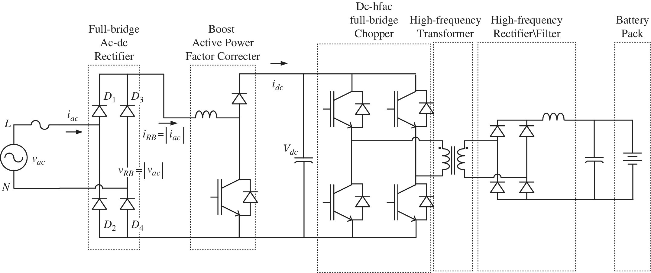
Figure 14.11 Automotive standard charger.
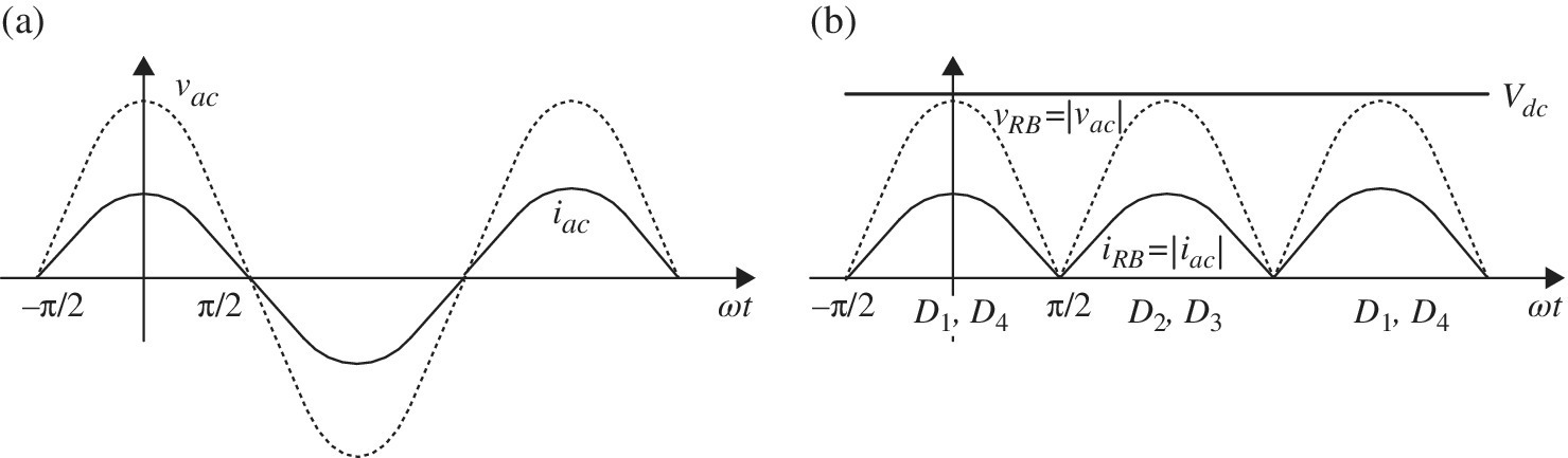
Figure 14.12 Power‐factor‐corrected waveforms: (a) input and (b) rectifier.
A more detailed overview of the EV battery charging system is shown in Figure 14.13. This charging system is representative of the on‐board conductive systems. The circuit has a number of different functions as follows:
- RCCB: The residual current circuit breaker (RCCB) detects an imbalance in the line and neutral currents, usually between about 5 to 20 mA, and triggers a circuit breaker to take the charger off‐line to prevent fatalities. This circuitry is also known as a ground‐fault circuit interrupter (GFCI).
- EMI filter: Switching power electronics can generate significant radiated and conducted noise, known as electromagnetic interference. A high‐current filter with common‐mode and differential‐mode stages is required to meet legal emission standards in the United States (FCC) and the EU (VDE). FCC Part 15b is commonly referenced in the United States, while the VDE B standard is commonly referenced in Europe.
- Rectifier: A simple diode bridge rectifies the 50/60 Hz ac waveform.
- Boost PFC: A boost converter, typically switching at tens or hundreds of kHz, chops up the low‐frequency rectified power and boosts it to a voltage level of about 400 Vdc, a value higher than the peak ac value.
- Dc link: An electrolytic capacitor is usually used for bulk storage to filter the 50/60 Hz component.
- Dc‐hfac chopper: A full‐bridge or H‐bridge converter is used to chop the nominal 400 V dc link voltage into a high‐frequency pulse stream going from ‐400 V to +400 V at the switching frequency.
- Transformer: the high‐frequency pulse stream is galvanically isolated for safety by the transformer. The pulse stream must be high frequency in order to minimize the size and weight of the transformer.
- Rectifier‐filter: The output of the transformer secondaries are rectified and filtered to create dc current to charge the battery.
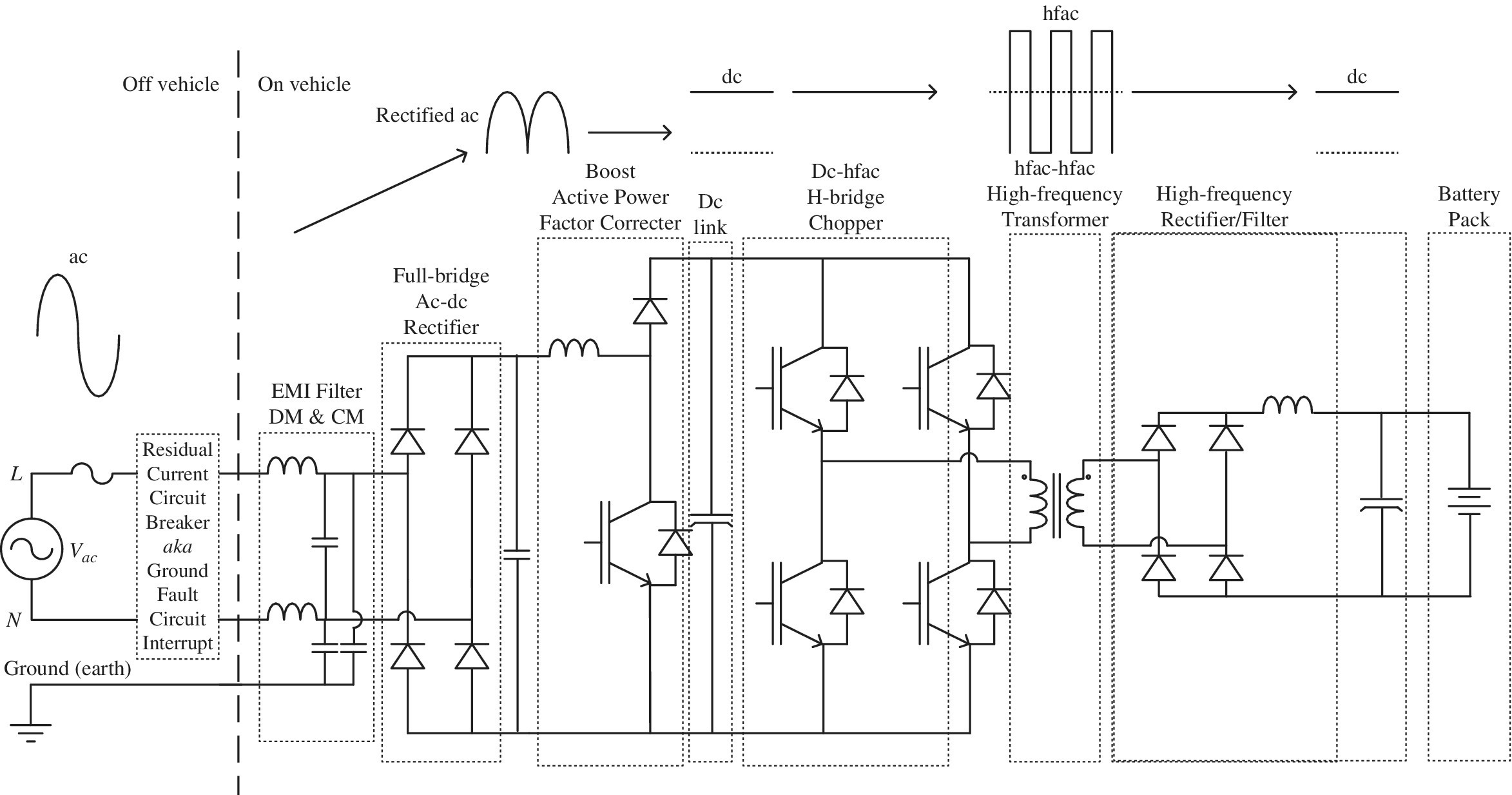
Figure 14.13 Conductive battery charging system.
14.5 Charging Standards and Technologies
A number of charging standards have emerged or are emerging globally. A global standard, IEC 62196, has been developed by the International Electrotechnical Commission (IEC) and acts as an umbrella standard for a number of the charging standards. The global standard covers the basics of power and communication interfaces, while the various charging standards describe the mechanical and electrical specifications of the particular plug and socket assemblies.
The main charging standards are
- SAE J1772 for use in North America and for ac and dc charging.
- VDE‐AR‐E 2623‐2‐2 for use in Europe and for single‐phase and three‐phase ac charging.
- JEVS G105‐1993, known as CHAdeMo and developed in Japan, for use globally for high‐power dc charging.
Tesla vehicles can be charged from a dedicated 240 V Tesla wall charger or by using a standard plug connected to a standard 240 V socket. The ac charger is on‐board. The Tesla vehicles can interface to SAE and VDE outlets by using an adapter.
14.5.1 SAE J1772
This standard has been developed by the Society of Automotive Engineers (SAE) for use in North America [1,2]. The standard covers a number of different power levels. Level 1 charging is for low‐power convenience charging using a standard 120 V outlet and supplying up to 1.44 kW or 1.96 kW maximum, depending on the outlet, whereas the Level 2 standard installed home charger would feature up to 19.2 kW, if available. Above these power levels, the standard includes options for high‐power off‐board dc charging. The various power levels for the SAE standard are presented in Table 14.1.
Table 14.1 SAE J1772 levels
| Voltage | Max. Continuous Current | |
| Ac Level 1 | 120 V (input ac) | 12/16 A (input ac) |
| Ac Level 2 | 240 V (input ac) | <80 A (input ac) |
| Dc Level 1 | 50–500V (output dc) | 80 A (output dc) |
| Dc Level 2 | 50–500V (output dc) | 200 A(output dc) |
The SAE standard also enables use of a combined socket featuring ac and dc which is known as the SAE J1772 Combo or CCS Combo.
The SAE J1772 Level 2 plug features three power contacts – line, neutral, and ground – and two signal contacts. A sample socket is shown in Figure 14.14(a).
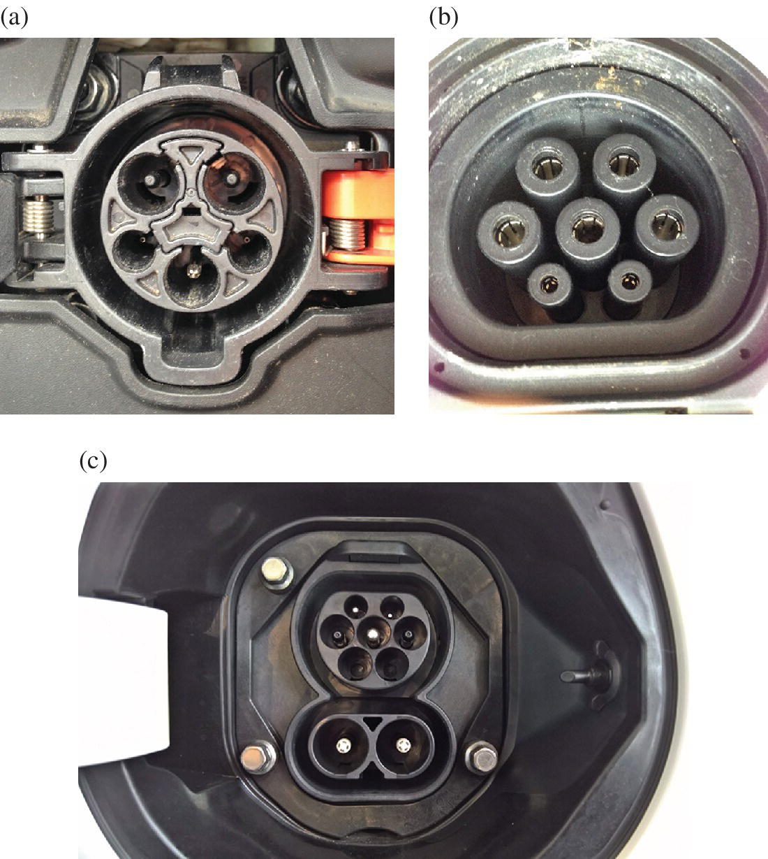
Figure 14.14 (a) SAE J1772 Level 2 socket, (b) VDE‐AR‐E 2623‐2‐2 plug, and (c) VDE‐AR‐E 2623‐2‐2 plus SAE Combo socket.
14.5.2 VDE‐AR‐E 2623‐2‐2
The VDE‐AR‐E 2623‐2‐2 standard has been developed for use in Europe. It facilitates the use of three phase, in addition to single phase, as three phase is widely available in parts of Europe. The standard includes five power wires – three lines, a neutral, and a ground – and two signal wires, as shown in Figure 14.14(b), and is often known as the Mennekes connector. This standard can be matched with the SAE high‐power dc charging standard socket, as shown in Figure 14.14(c), to create a version of the CCS Combo.
14.5.3 CHAdeMo
Several thousand high‐power chargers have been installed globally using the CHAdeMO standard. The basic high‐power charger is 40 kW. The 40 kW charger, plug, and socket are all shown in Figure 14.15.
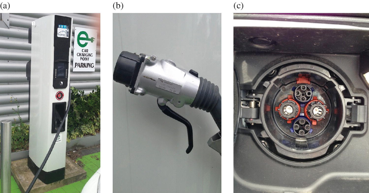
Figure 14.15 CHAdeMO: (a) off‐board dc charger, (b) plug, and (c) on‐board socket.
14.5.4 Tesla
The Tesla residential charger is designed to operate using commonly provided outlets. The vehicle comes with an adapter set which allows the charger to interface to the available power or off‐board charging outlet as shown in Figure 14.16(a). The charger cable plug to the vehicle is shown in Figure 14.16(b).
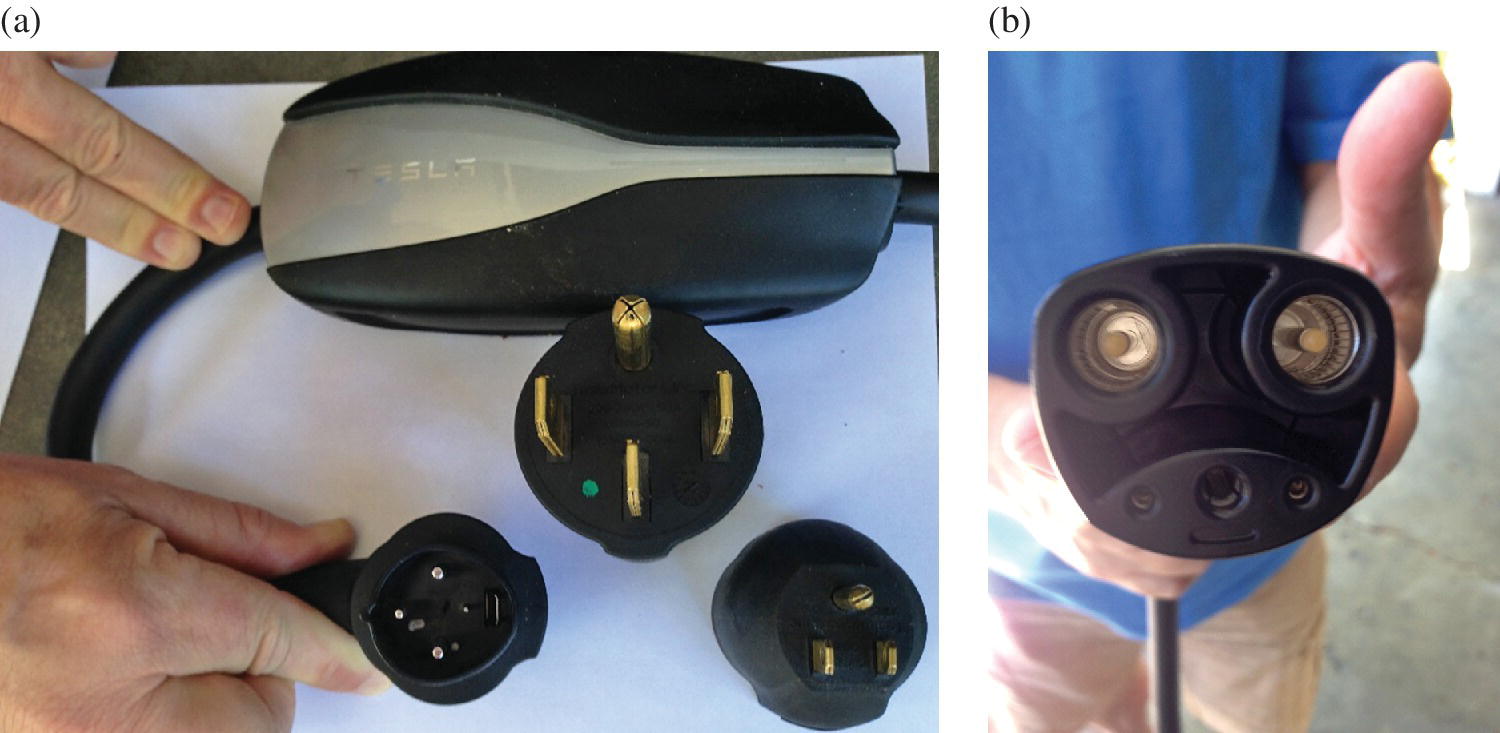
Figure 14.16 Tesla plug adapters and charging plug.
14.5.5 Wireless Charging
14.5.5.1 Inductive
Wireless charging or inductive charging is a method of transferring electrical power from the source to the load magnetically rather than by direct ohmic contact. The technology offers the advantages of galvanic isolation, safety, connector robustness, and durability in power delivery applications where harsh or hazardous environmental conditions may exist. Examples of these applications are mining and sub‐sea power delivery and EV battery charging. The General Motors EV1 featured many new technologies including a radically new design for inductively coupled battery charging.
The basic principle underlying inductive coupling is that the two halves of the inductive coupling interface are the primary and secondary of a separable two‐part transformer. When the charge coupler (i.e., the primary) is juxtaposed with the vehicle inlet (i.e., the secondary), power can be transferred magnetically with complete electrical isolation, as with a standard transformer. The coupler and vehicle inlet featured in the EV1 are shown in Figure 14.17(a). The coupler is attached via the cable to the off‐vehicle charging module. When the coupler is inserted into the vehicle inlet, power from the coupler is transformer‐coupled to the secondary, rectified, and fed to the battery by the battery cable. Note that the coupler contains a ferrite block or “puck” at the center of the primary winding to complete the magnetic path when the coupler is inserted into the vehicle inlet. The disassembled transformer components are shown in Figure 14.17(b).
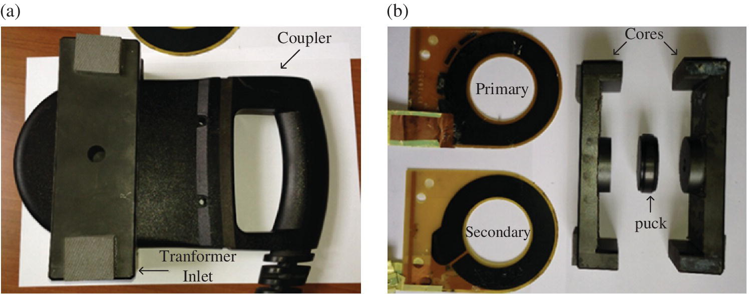
Figure 14.17 EV1 coupler and vehicle inlet.
An off‐vehicle high‐frequency power converter feeds the cable, coupler, vehicle‐charging inlet, and battery load. The EV user physically inserts the coupler into the vehicle inlet where the high‐frequency power is transformer‐coupled, rectified, and fed to the battery. The technology was researched and productized at levels ranging from a few kilowatts to tens of kilowatts, with a high‐power demonstration at 120 kW [3–6]. A recommended practice for inductive charging of EVs, SAE J1773, was published by the SAE. The specifications, as outlined in SAE J1773, for the coupler and vehicle inlet characteristics were to be considered when selecting a driving topology. Among the most critical parameters are the frequency range, the low magnetizing inductance, the high leakage inductance, and the significant discrete parallel capacitance. The off‐vehicle EV1 charge module features a frequency‐controlled series‐resonant converter. Driving the SAE J1773 vehicle interface with the series‐resonant converter results in a four‐element topology with many desirable features. This resonant topology is discussed in detail in Chapter 12, Section 12.4.
14.5.5.2 Wireless
The inductive charging system developed by GM is no longer used as the market shifted to conductive standards. However, new wireless charging standards are being developed for EVs as wireless charging is once again being viewed positively for developing the EV market. An interesting application of wireless charging is driverless vehicles, as charging can be facilitated without human actions. Recent interest in wireless charging has been in loosely coupled transformer systems. The principles are similar to the inductive coupling just described, with the difference that the transformer primary and secondary assemblies are spaced many centimeters apart and have relatively greater leakage inductances.
Worldwide standards are being developed. SAE J2954 is the SAE standard. The technology is also dependant on the types of resonant circuits discussed in Chapter 12 for application to inductive coupling. Additional safety issues must be addressed, such as the effects of radiation on humans and animals and the presence of metal objects in the magnetic fields.
14.6 The Boost Converter for Power Factor Correction
The front‐end of the charger is a power‐factor‐correction stage utilizing a boost converter. An example of an automotive charger is shown in Figure 14.18. The charger features an interleaved boost and so has two boost inductors, shown with an L. The input (IP) power first flows through the EMI filter (EMI) and is then rectified (R) and boosted (Q+D, L). The charger requires a significant electrolytic bulk capacitor stage (C) in order to filter the 50/60 Hz ripple. The full‐bridge converter stage features the power transformers (Xo), the full‐bridge switches and diodes (Qo+Do), the output rectifier (Ro), the output inductor (Lo), and output filtering (EMIo). The full‐bridge converter is discussed in depth in Chapter 12. The focus of this section is on the boost PFC, as shown in Figure 14.19(a).
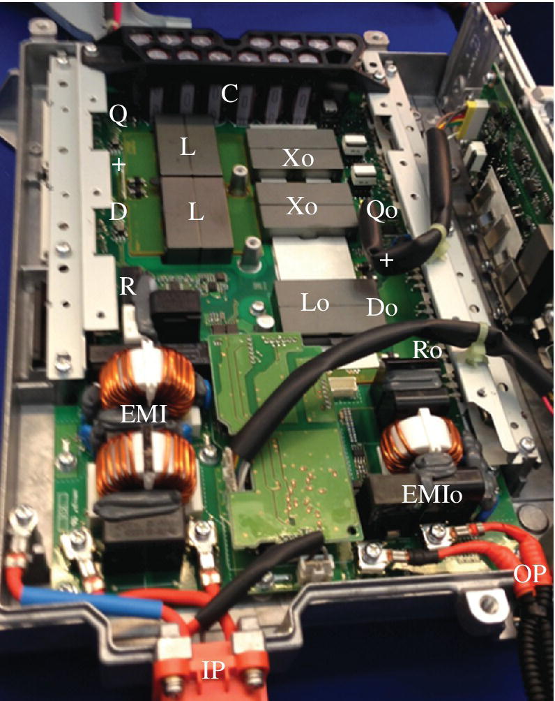
Figure 14.18 Automotive EV charger.
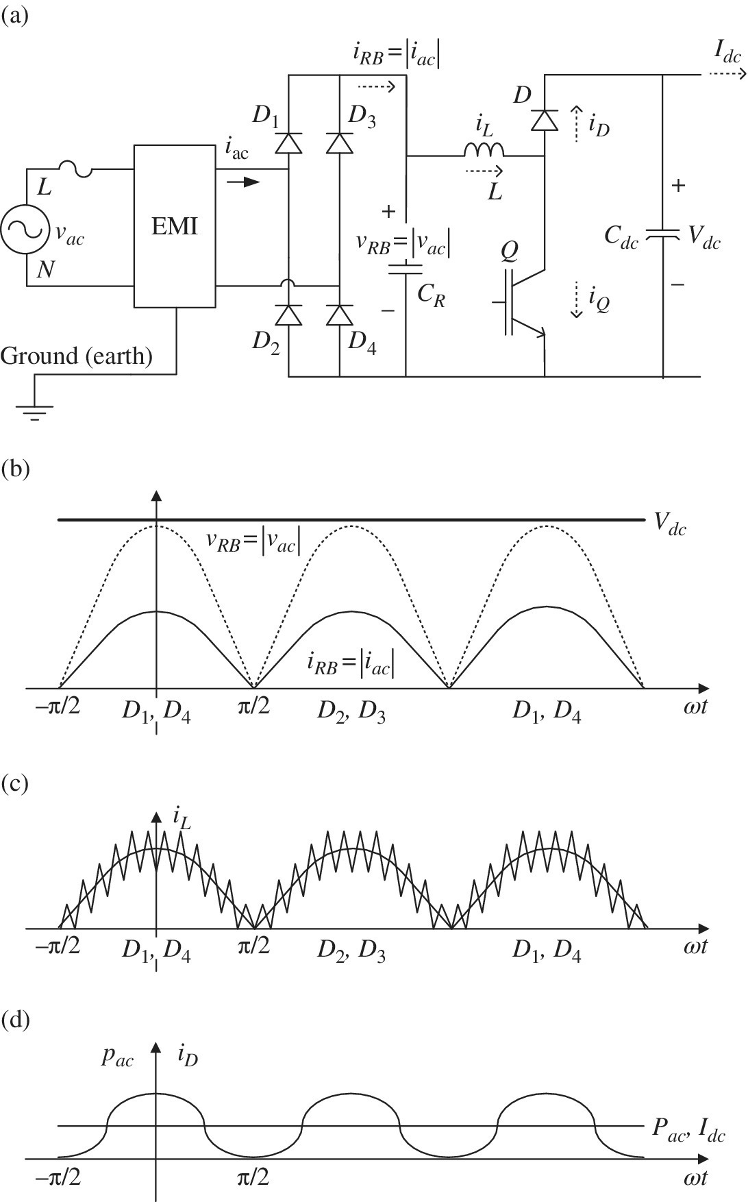
Figure 14.19 Boost PFC and waveforms.
14.6.1 The Boost PFC Power Stage
The input current is controlled to be in phase with the supply voltage. This is achieved by using two control loops: an inner current loop and an outer voltage loop. The converter typically achieves very high power factors with values greater than 0.99 being reasonable at full load [7–9].
The ac voltages and currents are rectified by the input bridge. Let the ac voltage be
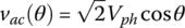
Using the boost PFC, the ac current is controlled to be in phase with the voltage:
The voltage vRB and current iRB from the rectifier bridge are
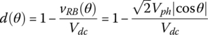
The boost converter controls the inductor current iL to be in phase with the rectified input voltage vRB, as shown in Figure 14.19(b) The inductor current carries the PWM ripple current as shown in Figure 14.19(c).
The capacitor at the output of the rectifier CR is there to filter the PWM ripple current of the inductor.
The size of the dc link capacitor in a PFC boost converter is based on three factors: (1) the desired hold‐up time of the capacitors, (2) the current rating and aging of the electrolytic capacitors, and (3) the low‐frequency voltage ripple. All three factors must be considered when designing the power and control stages. The dc link capacitor is usually a bank of bulky electrolytic capacitors, which are sized to minimize the low‐frequency voltage ripple due to the high second harmonic of the dc link current.
The EMI stage provides common‐mode and differential‐mode EMI filtering in order to meet the applicable EMC standards [10–13]. It is common for EMI stages to comprise 10% to 20 % of the volume of the charger or of the generic power converter.
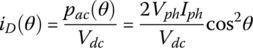
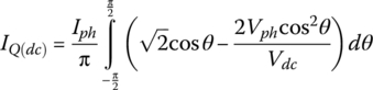
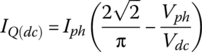
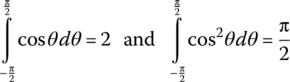
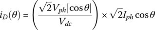
The power pulled from the ac source pac has a pulsing sine2 characteristic given by

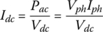
with an average power Pac given by

The characteristic of the power is as shown in Figure 14.19(d). The input power pulses from zero to twice the average power with a sine‐squared (sine2) characteristic.
If we consider the low‐frequency characteristic of the diode current, then the diode current also has a low‐frequency sine2 characteristic at twice the line frequency as shown in Figure 14.19(d). Neglecting PWM, the low‐frequency dc link power is given by

If we ignore the rectifier and boost power loss, the instantaneous dc link power pD equals the input power pac:

and so
Thus, the boost diode has a similar low‐frequency sine2 current characteristic, with power pulses from zero to twice the average power as shown in Figure 14.19(d). The average of the diode current equals the dc link current Idc and is given by
This low‐frequency current at twice the line frequency is typically filtered by the dc link capacitor Cdc. It is also an option in battery chargers to have the sine2 current flow into the battery, significantly reducing the requirement for the dc link capacitor [14]. However, sine2 charging, as it is known, increases the ripple current flowing into the battery.
14.6.2 Sizing the Boost Inductor
The boost inductor is sized in order to limit the ripple current and reduce harmonics and EMI. From the analysis of the CCM boost in Chapter 11 Section 11.4.1, the duty cycle of the boost switch is given by
The peak‐to‐peak ripple current is
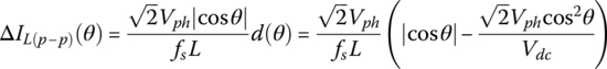
and so the ripple current magnitude clearly varies with duty cycle.
14.6.2.1 Example: Sizing the Inductor
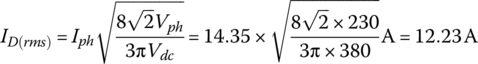
A 3.3 kW PFC boost is designed for a nominal input voltage of 230 V, 50/60 Hz with an input voltage ranging from a low line of 180 V to a high line of 265 V. Determine the value of the boost inductor and the peak inductor current if the switching frequency is 100 kHz and the peak‐to‐peak ripple ratio is 20% of the peak low‐frequency current at the peak of the nominal input voltage. The dc link voltage is 380 V. Ignore the power loss.
Solution:
The rms input current is
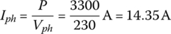
The peak of the input current is

The peak‐to‐peak ripple current at the peak of the input voltage is

The duty cycle at the peak of the input voltage is

The required inductance is determined by rearranging Equation (14.14):
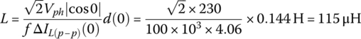
The peak current in the inductor is the sum of the peak of the line current and half of the peak‐to‐peak ripple:
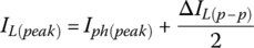
In this case:

Once the peak and rms currents are known, the inductor can be sized as covered in Chapter 16, Section 16.3.7, using the area‐product method. The rms input current can be used as a reasonable approximation for the rms inductor current.
14.6.3 Average Currents in the Rectifier
The input rectifier diodes alternately conduct. Diodes D1 and D4 conduct during the positive half cycle, while diodes D2 and D3 conduct during the negative half cycle.
The average current in the rectifier diodes IR(dc) for a half cycle is
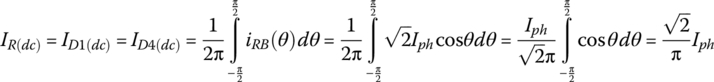
The rms current in the rectifier diodes IR(rms) for a half cycle is
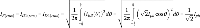
The values of the dc and rms currents in diodes D2 and D3 are the same as in diodes D1 and D4.
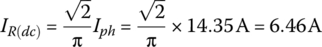
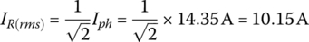
14.6.3.1 Example: Input Rectifier Power Loss
Determine the power loss in the input rectifier stage of the earlier example if each rectifier has the following parameters: Vf0 =0.8 V and rf = 10 mΩ.
Solution:
The average current in the rectifier diodes for a half cycle is
The rms current in the rectifier diodes for a half cycle is
Per the section on semiconductor losses in Chapter 11, Section 11.5, the conduction loss per rectifier diode is
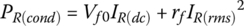
In this case:

The loss in the rectifier bridge PRB is four times the loss in a single rectifier diode:

For this example:

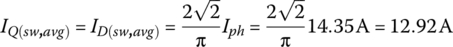
14.6.4 Switch and Diode Average Currents
The duty cycle of the boost switch is given by Equation (14.13).
The low‐frequency time‐averaged current in the switch can be approximated by
Substituting in Equation (14.4) and Equation (14.13) yields:
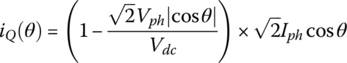
or
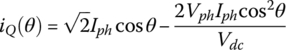
The average current in the switch is given by
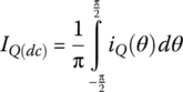
Substituting Equation (14.22) into Equation (14.23) yields
which simplifies to
since
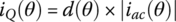
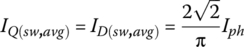
Similarly, the low‐frequency time‐averaged current in the boost diode is given by

which expands to
The diode conducts the current for half the period, and the average current is
which simplifies to
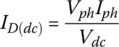
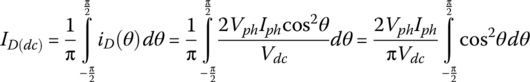
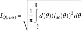
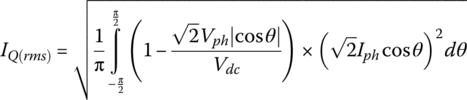
14.6.5 Switch, Diode, and Capacitor RMS Currents
The rms current in the boost switch can be approximated by
Substituting in Equation (14.4) and Equation (14.13) gives
which simplifies to
Since
the rms current in the switch is given by
Similarly the rms current in the boost diode is given by
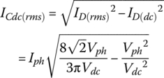
The rms current in the high‐voltage dc link capacitor ICdc(rms) is simply given by
14.6.6 Power Semiconductors for Charging
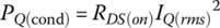
While the silicon IGBT and the silicon diode are dominant for low‐to‐medium switching frequencies, the silicon MOSFET is typically preferred at higher switching frequencies for low‐ and medium‐range voltages (<600 V). The conduction loss in the MOSFET can be simply modeled by the drain‐source on‐resistance, typically designated RDS(on). The maximum RDS(on) is usually specified for the component. A characteristic of the power MOSFET is that the on‐resistance typically doubles between 25°C and 120°C.
The MOSFET conduction loss is given by
As RDS(on) increases with an index somewhere between the square and cube of the device voltage rating, the silicon MOSFET cannot compete with the silicon IGBT for higher voltages. However, the MOSFET is a competitive device for a high‐frequency PFC boost.
A significant source of power loss for the switching pole is the reverse recovery loss of the boost diode. This loss can be eliminated by employing the more expensive wide‐band‐gap silicon‐carbide (SiC) Schottky diode, which has no reverse recovery loss.
The average current in the diode and switch when switched is
Similar to the IGBT in Chapter 11, Section 11.5.1.3, the MOSFET switching power losses remain
It is assumed for simplicity that the switching loss for the SiC diode is zero.
In the final part of this section, the losses are estimated for the semiconductor switches in the boost PFC.
14.6.6.1 Example: Silicon MOSFET and SiC Diode Power Losses
The PFC boost converter of the examples used in this chapter features a representative silicon MOSFET and a SiC diode, nominally the part MKE 11R600DCGFC from manufacturer IXYS [15].
The nominal maximum RDS(on) of the device is specified as 0.165 Ω at 25°C, but increases to about 0.375 Ω at 125°C as shown in Figure 14.20(a).
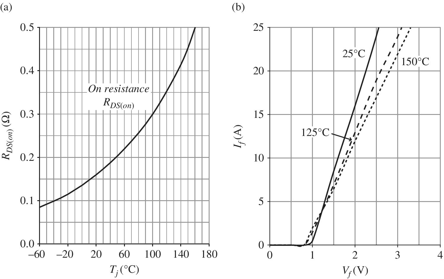
Figure 14.20 Representative 600 V, 15 A MOSFET and SiC diode conduction characteristics.
The diode conduction drops are shown in Figure 14.20(b) and can be modeled by Vf0 = 0.8 V and rf = 8.8 mΩ at 125°C.
The MOSFET switching losses are shown in Figure 14.21. The diode switching losses are ignored.
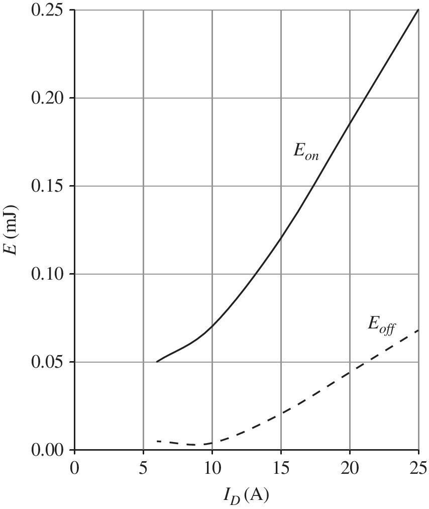
Figure 14.21 Representative 600 V, 15 A MOSFET (and SiC diode) turn‐on and turn‐off switching losses at 125°C and a test voltage of 380 Vdc.
Determine the MOSFET and diode power losses, assuming junction temperatures of 125°C.
Solution:
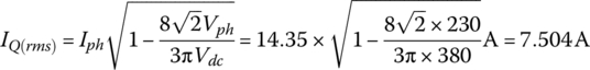
The switch rms current is
The MOSFET conduction loss is

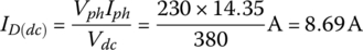
The diode average and rms currents are
The diode conduction loss is

For a sinusoidal excitation, the average switching current in the switch and diode is
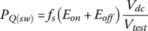
The turn‐on and turn‐off power loss in the switch is

where Eon = 0.1 mJ and Eoff = 0.013 mJ at 12.92 A from Figure 14.21.
The power losses in the switch and diode are

and

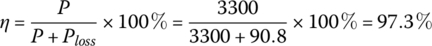
14.6.6.2 Example: PFC Stage Losses
If the equivalent series resistance of the inductor is Rcu = 50 mΩ, and the combined auxiliary power and stray power loss Paux is 15 W, determine the overall PFC converter power loss and efficiency.
Solution:
The inductor loss is

The auxiliary and stray loss is

The total loss is the sum of the losses in the inductor, the auxiliary circuits, the bridge rectifier, and the boost switch and diode:

The approximate efficiency is
References
- 1 SAE Electric Vehicle and Plug in Hybrid Electric Vehicle Conductive Charge Coupler, SAE J‐1772, Society of Automotive Engineers.
- 2 SAE Power Quality Requirements for Plug‐In Electric Vehicle Chargers, SAE J‐2894, Society of Automotive Engineers.
- 3 J. G. Hayes, Resonant Power Conversion Topologies for Inductive Charging of Electric Vehicle Batteries, PhD Thesis, University College Cork, 1998.
- 4 SAE Electric Vehicle Inductive Coupling Recommended Practice, SAE J‐1773, Society of Automotive Engineers, Draft, Feb. 1, 1995.
- 5 R. Severns, E. Yeow, G. Woody, J. Hall, and J. Hayes, “An ultra‐compact transformer for a 100 W to 120 kW inductive coupler for electric vehicle battery charging,” IEEE Applied Power Electronics Conference, pp. 32–38, 1996.
- 6 J. G. Hayes, N. O’Donovan, and M. G. Egan, “Inductance characterization of high‐leakage transformers,” IEEE Applied Power Electronics Conference, pp. 1150–1156, 2003.
- 7 N. Mohan, Power Electronics A First Course, Chapter 6, John Wiley & Sons, 2012.
- 8 S. Abdel‐Rahman, F. Stuckler, and K. Siu, PFC Boost Converter Design Guide 1200 W Design Example, Infineon Application Note, 2016.
- 9 Texas Instruments, UCC2817, UCC2818, UCC3817 and UCC3818 BiCMOS Power Factor Preregulator, Unitrode Products from Texas Instruments, revised 2015.
- 10 M. Nave, Power Line Filter Design for Switched‐Mode Power Supplies, Van Nostrand Reinhold, 1991.
- 11 H. W. Ott, Electromagnetic Compatibility Engineering, John Wiley & Sons, 2009.
- 12 P. Bardos, “Predicting the EMC performance of high‐frequency inverters,” IEEE Applied Power Electronics Conference, pp. 213–219, 2001.
- 13 M. Kacki, M. Rylko, J. G. Hayes, and C. R. Sullivan, “Magnetic material selection for EMI filters,” IEEE Energy Conversion Congress and Exposition, 2017.
- 14 M. G. Egan, D. O’Sullivan, J. G. Hayes, M. Willers, and C. P. Henze, “Power‐factor‐corrected single‐stage inductive charger for electric‐vehicle batteries,” IEEE Transactions on Industrial Electronics, 54 (2), pp. 1217–1226, April 2007.
- 15 Website of IXYS Corp., www.ixys.com.
Further Reading
- 1 N. Mohan, T. M. Undeland, and W. P. Robbins, Power Electronics Converters, Applications and Design, 3rd edition, John Wiley & Sons, 2003.
- 2 R. W. Erickson, Fundamentals of Power Electronics, Chapter 17, Kluwer Academic Publishers, 2000.
- 3 M. Yilmaz and P. T. Krein, “Review of battery charger topologies, charging power levels, and infrastructure for plug‐in electric and hybrid vehicles,” IEEE Transactions on Power Electronics, 28 (5), pp. 2151–2169, May 2013.
- 4 R. Ryan, J. G. Hayes, R. Morrison, and D. Hogan, “Digital control of an interleaved BCM boost PFC converter with fast transient response at low input voltage,” IEEE Energy Conversion Congress and Exposition, 2017.
Problems
- 14.1 Determine the following for the converter example used in this chapter when the line voltage is (i) 180 V and (ii) 265 V, at an output power of 3.3 kW: input current, rectifier bridge and inductor power losses, switch and diode average and rms currents and losses, overall converter loss, and efficiency. [Ans. (i) Iph = 18.33 A, PRB = 33.1 W, PL = 16.8 W, IQ(rms) = 12.04 A, ID(dc) = 8.68 A, ID(rms) = 13.82 A, PQ = 69.9 W (Eon ≈ 0.025 mJ, Eoff ≈ 0.13 mJ), PD = 8.6 W, Ploss = 143.4 W, Eff = 95.8%; (ii) Iph = 12.45 A, PRB = 21.0 W, PL = 7.8 W, IQ(rms) = 5.02 A, ID(dc) = 8.68 A, ID(rms) = 11.39 A, PQ = 18 W, PD = 8.1 W, Ploss = 69.9 W, Eff = 97.9%]
- 14.2 A 2 kW PFC boost is designed for a nominal input voltage of 230 V with an input voltage ranging from a low line of 180 V to a high line of 265 V. The dc link voltage is 380 V. Assume an equivalent series resistance of the inductor of 50 mΩ and auxiliary and a stray power loss of 15 W. Use the semiconductor characteristics of Section 14.6.6.1.
- Determine the value of boost inductor if the switching frequency is 60 kHz and the peak‐to‐peak ripple ratio is 15% of the peak low‐frequency current at the peak of the nominal input voltage.
- Determine the following at the nominal voltage: input current, rectifier bridge and inductor power losses, switch and diode average and rms currents, and switch and diode losses, overall converter loss, and efficiency.
- 14.3 A 6.6 kW PFC boost is designed for a nominal input voltage of 220 V, 50/60 Hz. The switching frequency is 40 kHz and the peak‐to‐peak ripple ratio is 10% of the peak low‐frequency current at the peak of the nominal input voltage. The dc link voltage is 380 V.
- Determine the values of the boost inductor and the peak inductor current.
- Determine the power losses in the boost switch if the RDS(on) of the MOSFET is 0.19 Ω, and the turn‐on and turn‐off energy losses are given by the curves in Figure 14.22. Note that the curves are for a dc link voltage of 380 V.
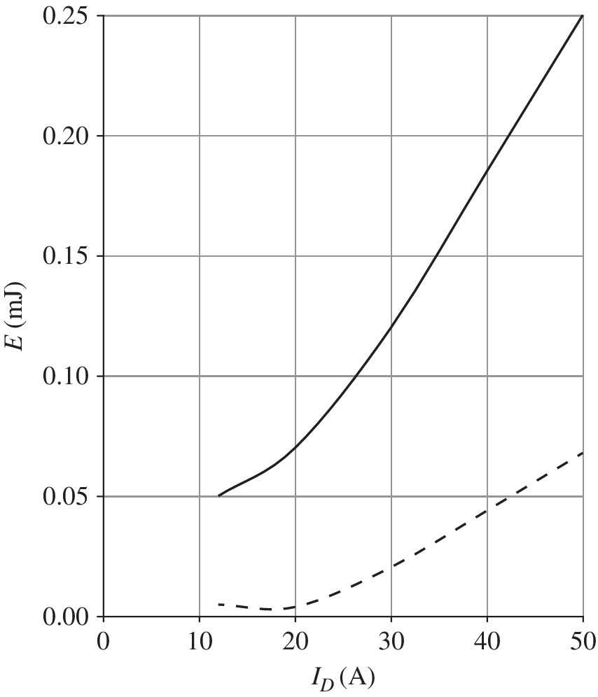
Figure 14.22 Representative 600 V, 30 A MOSFET (and SiC diode) Turn‐on and turn‐off energy curves at 380 Vdc. [Ans. 332 μH, IL(peak)= 44.5 A, PQ = 57 W]
Assignments
- What are the voltages, currents, frequency, and wiring configurations in your region?Which charging standards are used in your region?