When designing a complex system for a FPGA, there is nothing to stop you from putting all your Verilog code into one module. However, splitting things up makes it easier for others to understand what you have done. This is so because they can assume that the component modules perform the role they are supposed to and therefore see a bigger picture of how all the modules work together before getting into the nitty-gritty of how each one works. Breaking things up into a number of modules also makes it a lot easier to take a module that you used in one project and use it in another or to share it with someone else to use in their project.
When you create a project with more than one module, you will always have a top-level module. This is the module that brings all the submodules together as well as the module that will have a UCF associated with it to map the IO pins of the FPGA to the signals in the design.
In this chapter, you will start by using a seven-segment decoder module along with the counter module of Chapter 4 and expanding the example until eventually you have a simple decimal counter that counts up and down on the seven- segment multidigit display when you press the UP and DOWN switches.
You can either build the projects up yourself following the instructions here or download the completed projects from GitHub, as described at the end of Chapter 2 .
The first reusable module that we are going to build is a seven-segment decoder. This will have a 4-bit input. The number at this input or, rather, the numbers 0 to 9 will be decoded into the correct segment pattern to display the number on a seven-segment display.
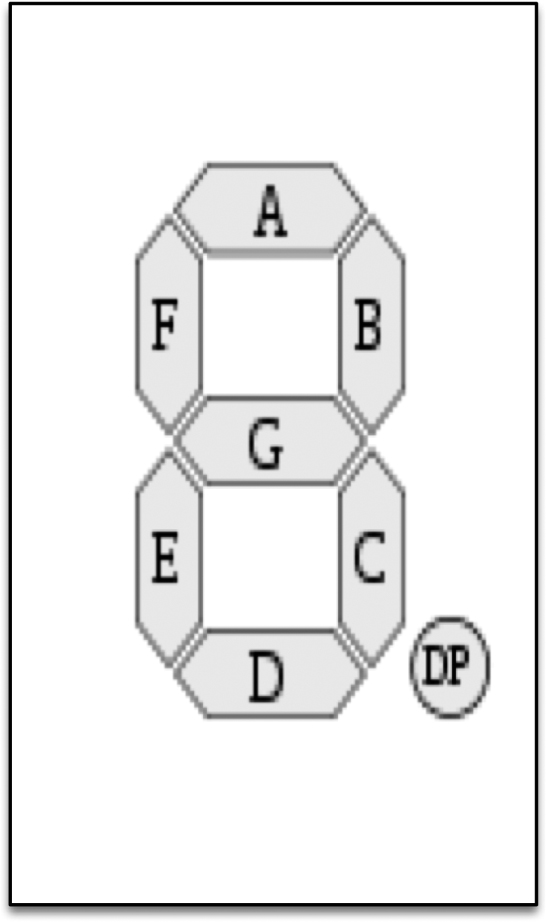
Figure 5-1 shows how the segments of a seven-segment display are organized. Each segment is given a letter A–G with an additional connection to the decimal point (DP).

Figure 5-1 Seven-segment display.
Create a new project called decoder_7_seg. You can also find this project in the downloads for this book where it is called ch05_decoder_7_seg. See the section at the end of Chapter 2 for downloading this book’s examples.
Create a new Verilog source file in an src directory, and call the file “decoder_7_seg.” Write or paste the following code into it:
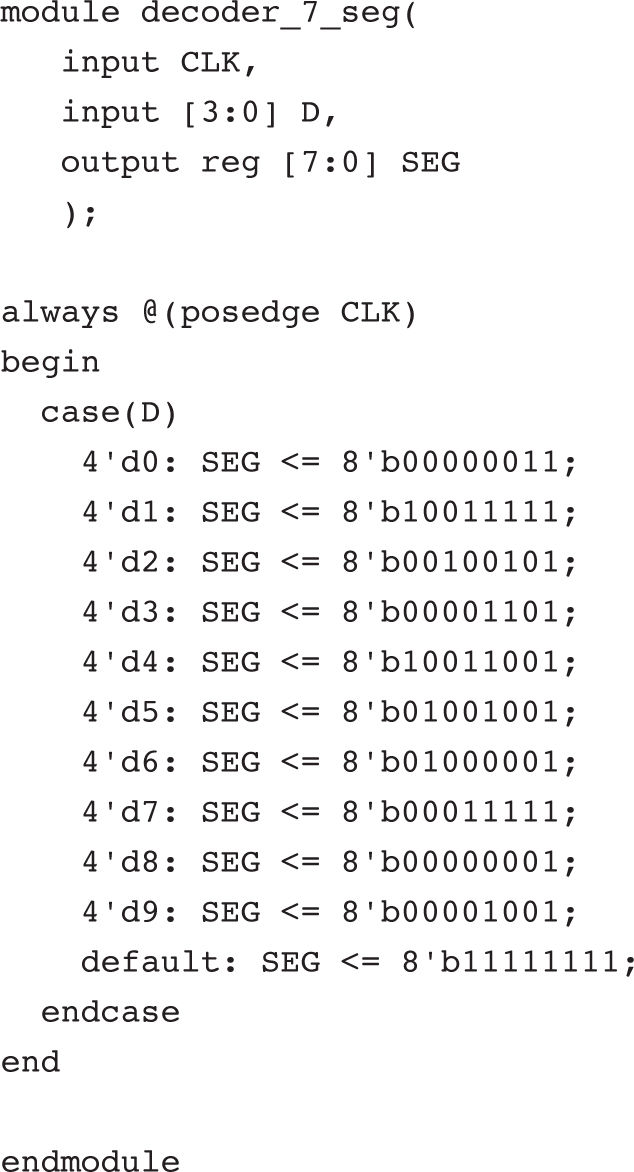
Starting with the module header, there is a CLK (clock) input because we want the module to synchronize with the FPGA clock. There is also a 4-bit input D that will contain the number to be displayed and an 8-bit register output
that will be the bit pattern to appear on the segments of the LED.
The always
block synchronizes on the CLK and contains a new construct called a case statement
. The case statement is a more concise way of writing a whole load of if
commands that all have the same value as a condition. Here input D is the value of interest to the case statement. If D is 0, then the output segments (SEG) are set to the bit pattern 00000011
. A zero indicates that the segment should be lit. Thus, referring to Figure 5-1
, this says that segments a, b, c, d, e, and f should all be lit, leaving just g (in the middle) and the decimal place unlit. Each value of D has its own bit pattern.
The default
option at the end of the case statement defines what SEG should be set to if none of the values of D match. Because we have a 4-bit value in D, this means that any value over decimal 9 will result in all the segments being off.
This module is designed as a useful component to drop into other projects. To try it out, you need to create another module (one not designed for reuse) that will use this module but also do things like disabling all the digits except one. So create a new source file called seg_test, and put the following code into it:

This module’s inputs and outputs are
![]() CLK: clock
CLK: clock
![]() D: Data, 4 bits, each of which will be allocated to a slide switch
D: Data, 4 bits, each of which will be allocated to a slide switch
![]() SEG: 8 bits, one for each segment
SEG: 8 bits, one for each segment
![]() DIGITS: 4 bits, to control the digits that are to be enabled
DIGITS: 4 bits, to control the digits that are to be enabled
Note how DIGITS is initialized to just enable the first digit using the inverted logic of a zero meaning enabled. Then comes the really interesting line:
![]()
This creates a decoder_7_seg called “decoder,” and its parameters between “(” and “)” specify how “decoder” will be connected to the wires and registers in the seg_test module. The names starting with a dot name the parameter in the decoder and then inside a further set of parentheses are references to “wires” or “regs” in seg_test to which the names should be linked.
Finally, you need to create a UCF for the project. The one for the Mojo is listed next; you will find equivalents for the other boards in this book’s downloads (see Chapter 2 ).
To test out the project, upload it onto your board, and then try dialing in different values on the slide switches. Figure 5-2 shows this in action.
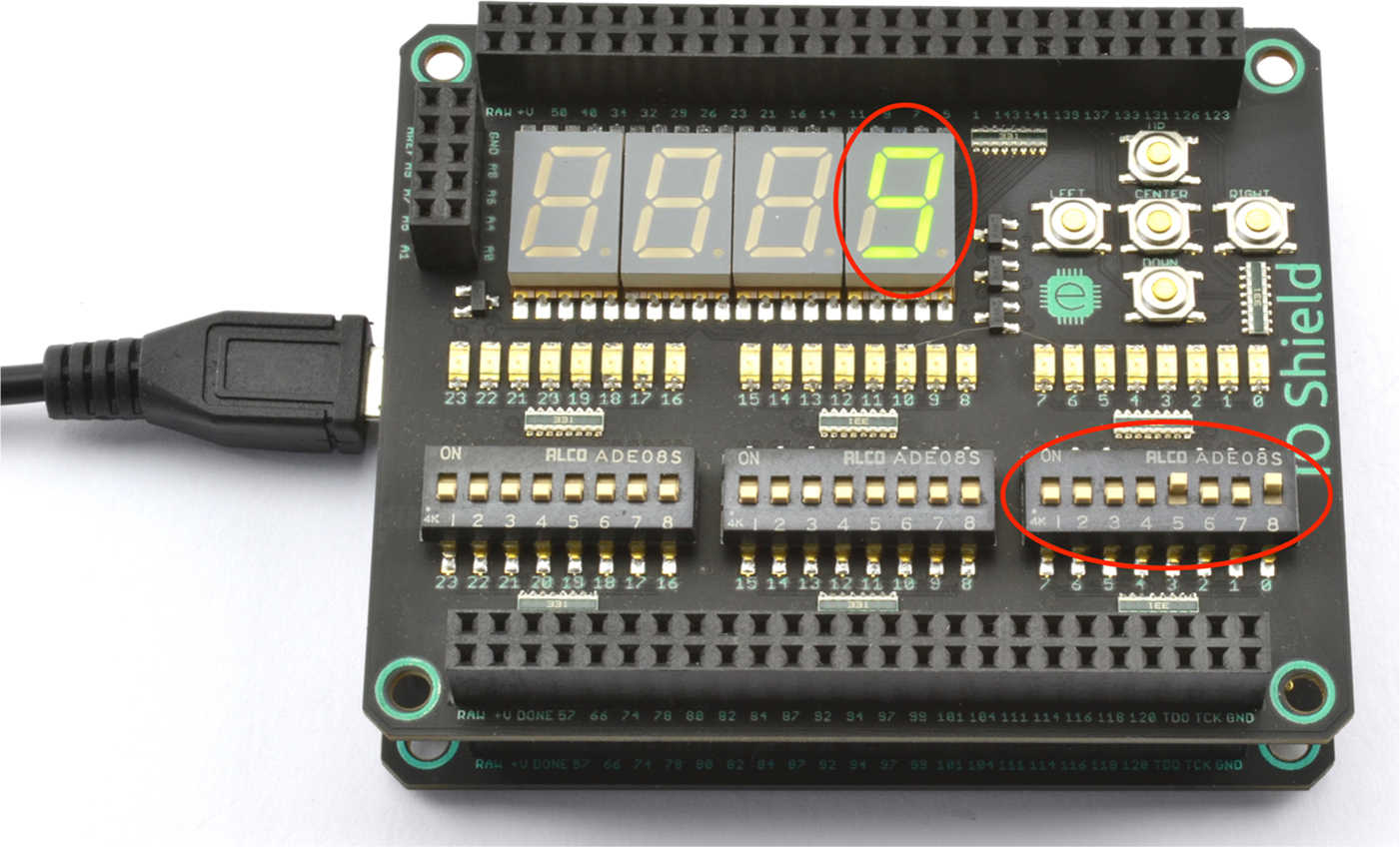
Figure 5-2 Testing the seven-segment decoder module.
When you were experimenting with the counter project, you may have noticed some switch bounce that caused the counter to skip over some numbers. We can do something about this by creating a debouncing module that we can use in any project where we use a switch.
When it comes to push switches, there are actually three problems to solve. First, there is a problem that a button press is by its nature not going to be synchronized to the clock. Second, we have the problem of actually removing any unwanted transitions resulting from the mechanical contacts of the switch bouncing. Finally, there is the problem that you are usually interested in triggering things on a transition for a button from OFF to ON (or vice versa) rather than at any particular time it is ON or OFF (its state).
We can lump these three features together into one very useful module that takes a potentially bouncy switch as an input and gives us as an output a clean, synchronized binary state of the button, along with a pair of useful extra outputs that go high for a single clock cycle when the button transitions. You can find the project illustrating switch debouncing in the project “debounce.” You may wish to have this open in ISE because the code is explained.
The code for this is adapted from www.fpga4fun.com/Debouncer.html and www.eecs.umich.edu/courses/eecs270/270lab/270_docs/debounce.html .
The first step is to synchronize the push switch to the clock using a pair of registers. Here is the listing for debouncer.v together with explanations of the code. You can find a project illustrating the use of this module in the download ch05_debouncer file.
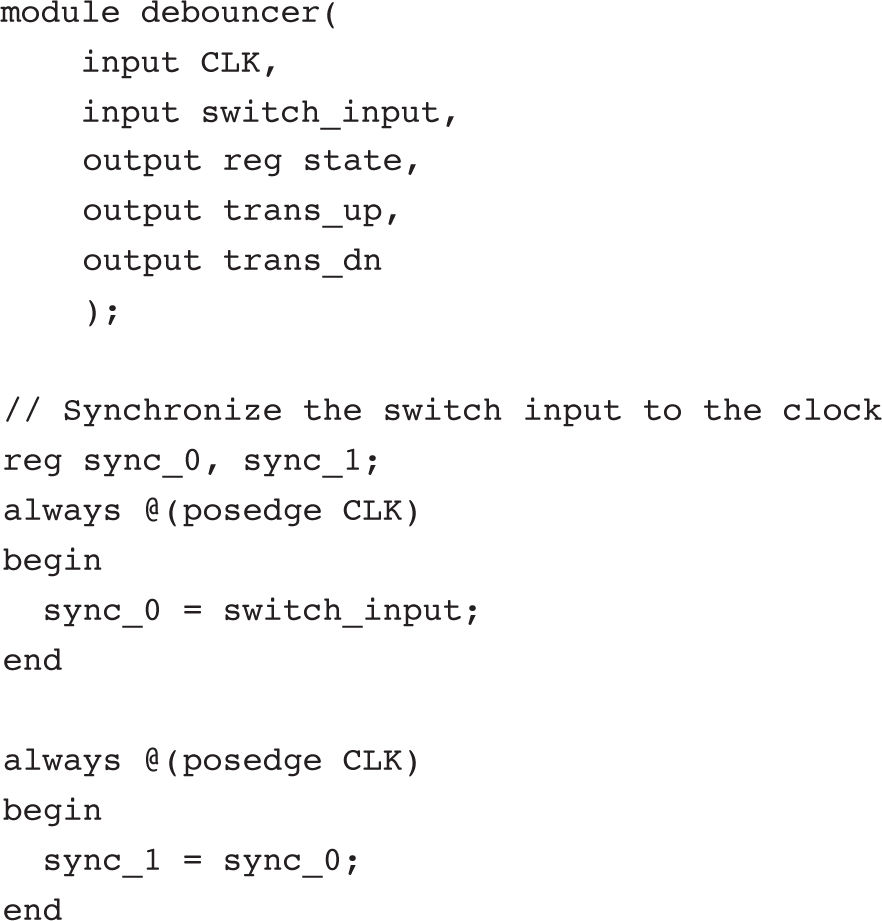
The output of the second register (sync_1
) is then used for the debouncing code:

The debouncing itself works by using a timer (in this case a 16-bit timer). This then ignores any transitions in the switch signal until the timer has counted to its maximum value. In the case of a 16-bit timer, this is 65,536 clock cycles, which for the 50-MHz clock of a Mojo is 65,536/50,000,000 = 1.3 ms. On an Elbert 2 with its 12-MHz clock, this will be 5.4 ms, and on the 32-MHz Papilio One, it will be 2 ms. Generally, the switch bouncing will settle out in well under a millisecond, and 5.4 ms is still a very short time as far as a user is concerned, so the code does not really need to be modified for the other boards used in this book despite their different clock speeds.
The idle
wire’s value is set to be the result of comparing state with sync_1
. If they are the same, then no switch transition in is progress, and idle
will have the value 1; otherwise, it will have the value 0. In common with such programming languages as Java and C, the ==
operator is used to compare values to see if they are equal.
To detect that the counter is maxed out, the logical &
operator is used. When used on a multibit register such as “count,” the result is all the bits being ANDed together. This state is associated with the wire finished
.
The main always
block is synced to the positive edge of the clock and, if nothing is happening, resets count to 0. If a transition is in progress, then the counter is incremented. When the counter is finished, the state
output is toggled. The ~
symbol means invert in Verilog.
It just remains to define the useful extra output values of trans_dn
and trans_up
, which will become high for one clock cycle as the button is pressed or released, respectively. This is accomplished by ANDing together the inverted output of the idle
signal, whether the timer has “finished” and then state
is output or, in the case of trans_dn
, the inverse of state
.

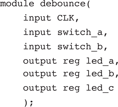
The test program for the debounce code illustrates how the module can be used for all three possible outputs. It uses two push buttons, each of which toggles the state of separate LEDs, one on trans_dn
(button pressed) and one on trans_up
(buttton released). A third LED simply mirrors the state of the first button.
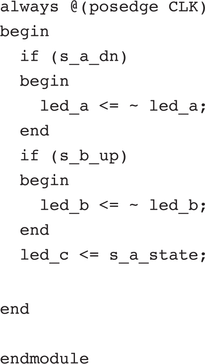
Three wires are defined, s_a_dn
(switch a down), s_b_up
and s_a_state
. These wires are then linked to three debouncers d1 to d3. Looking at the first of these debouncer lines of code, you can see that the debouncer has been given the name d1
, and then there are a number of parameters enclosed in parentheses. Each parameter is in the form of a pair, and each of these pairs is separated by a comma. The first parameter, .CLK
(CLK), links the CLK signal of the debouncer (the CLK preceded by a period) to the CLK used in this debounce test module.
The second parameter, .switch_input
(switch_a)
, links the switch_input
of the debouncer to switch_a
. The final parameter, .trans_dn
(s_a_dn)
, connects the trans_dn
output of the debouncer to the wire s_a_dn
. This repeats for the other two debouncer instances. However, these instances use the trans_up
and state
outputs of the debouncers, linking them to the wires s_b_up
and s_a_state
, respectively.

The always
block is synced to the positive edge of the clock and uses the wires linked to the outputs of the three debouncers to set the three LEDs.
Now that you have tamed our switch inputs, you do not need to worry about how this module works; you can just use it within any of your projects that needs switch debouncing. To illustrate this, in the next section, you will bring together both the debouncer and decoder_7_seg modules to make a third module that is a four-digit (three in the case of the Elbert 2) counter display.
This example (Figure 5-3 ) will display a number on the multidigit seven-segment display. Pressing the “Up” button will increment this number and the “Down” button will reset it to zero. You can find the files for this in the project “ch05_counter_7_seg.”

Figure 5-3 A multiplexed seven-segment display.
All three FPGA boards have multiplexed seven-segment LED displays. In the case of the Mojo (with IO Shield) and the Papilio (with LogicStart MegaWing), these are four-digit displays, and the Elbert 2 is a three-digit display. In all cases, the displays are wired up in much the same way. Figure 5-4 shows the schematic for the Mojo IO Shield’s display; the other boards are much the same but use different pins.
Figure 5-4 Schematic of the Mojo IO Shield’s display.
Each segment of a particular digit is connected to the same segments on the other digits. In other words, all the segments A
are connected together, all the segments B
are connected together, and so on. Each segment is then connected via a resistor (shown as R5 in Figure 5-4
) that is in turn connected to a general-purpose input-output (GPIO) pin.
This means that if you say set GPIO pin P8 HIGH, then all segments B would be enabled. Clearly, you need to be able to display different numbers on each digit. To do this, each digit is enabled in turn using the separate digit control pins and the segment pattern for that digit set before moving onto the next digit and setting a different segment pattern. This happens so fast that you don’t see any flicker—it just appears that each digit is displaying a different segment pattern.
Before wading into the detail, it’s worth taking a step back and looking at how the various modules used in this project will relate to each other (Figure 5-5 ).
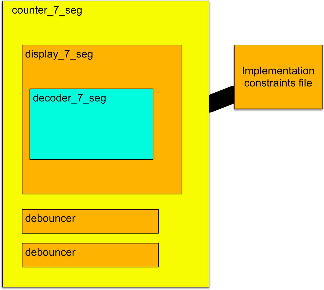
Figure 5-5 The modules used in the “counter_7_seg” project.
The module counter_7_seg is called the top-level module (more on this later). It is to this module that the UCF for your board will be attached. This module implements the logic of the counter: incrementing its value, and resetting it and making use of other modules that operate the display.
The counter_7_seg module has one instance of display_7_seg
and two instances of debouncer
within it. The display_7_seg module will be responsible for multiplexing the display and refreshing it so that it can display all the digits. The module display_7_seg itself contains the decoder_7_seg module that we created earlier. It will use decoder_7_seg to set the segment pattern of each digit in turn.
You have already learned about the two modules decoder_7_seg and debouncer, so we can start with the module display_7_seg. Here is the listing for display_7_seg.v together with explanations of the code:

As well as a CLK signal, the module has four (three for the Ebert 2) inputs for each of the digit positions called units
, tens
, hundreds
, and thousands
. The two
outputs are for the GPIO pins that will be assigned to control the segments and the digit enable
lines.
Three vectors are needed:
![]()
Digit_data
is a 4-bit register that will be assigned to the 4-bit number to be decoded for the digit currently being processed.
![]()
Digit_position
is a 2-bit counter that is used to keep track of which digit is currently being displayed.
![]()
Prescaler
is a 24-bit counter that is used to divide the CLK input to set the refresh rate. The prescaler does not need to be nearly as big as 24 bits, but this gives us options should we use a really fast FPGA.

Next, the display_7_seg module needs an instance of decoder_7_seg
to convert a 4-bit number into an 8-bit segment pattern. We only need one of these because it will be used for each of the digits in turn.
The D input of the decoder is connected to digit_data
, and the SEG vector is passed along again to the decoder:
![]()
Now comes the always
block, synched to the clock. This adds 1 to the prescaler counter. If the value of prescaler
has reached 50,000, then it’s time to refresh the next digit. The 50-MHz clock speed of the Mojo means that this will happen every millisecond. Four digits therefore will take 4 ms, resulting in a refresh frequency of 250 Hz, which is still far too fast for the human eye to see any flicker. You can, if you really want, change this value to suit the other board’s clock frequencies, but even with the 12-MHz clock of the Elbert 2, the refresh will be too fast for the flicker to be visible.

If the prescaler has reached its set value and its time for the next digit refresh, a series of updates now take place, to switch in the appropriate digit data.
First, the prescaler is reset to 0 to start the timer for the next digit refresh, and then digit_posn
is incremented. If digit_posn
is 0, then digit_data
is set to be units. The digit control pins (DIGIT) are then set to enable just the first digit. In this case, the binary pattern 1110
is used. It is 1110
rather than 0001
because the digit control pins are active LOW. A 0 means that that digit is enabled.
The same pattern is repeated for each of the other digit positions:
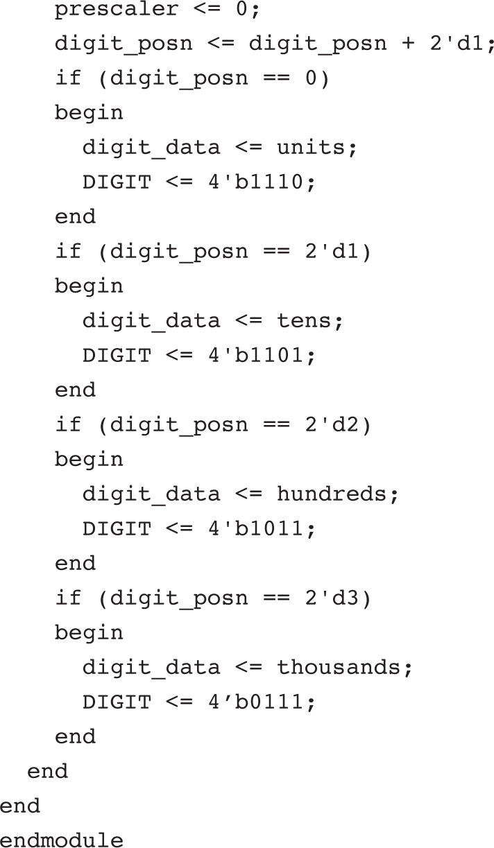
The 2-bit digit_posn
counter will automatically wrap around from 3 to 0, and so does not need to be explicitly reset. The Elbert 2 has only three digits, so the digit_posn
counter will need to be reset to 0 after the third digit has been displayed.
The counter_7_seg module is the top-level module that pulls everything together. The module’s parameters are all concerned with GPIO pins and will map onto the nets defined in the UCF file. Here is the listing for counter_7_seg.v together with explanations of the code:
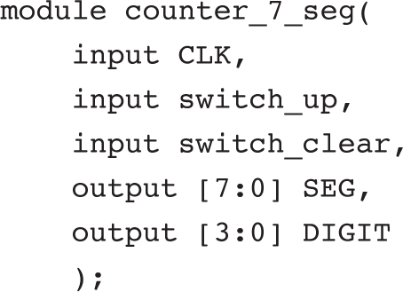
The project requires two push switches, one to increment the count and one to clear the display back to 0000. These switches are linked to wires and debounced using debouncer modules.

Four 4-bit registers are needed, one for each of the four digits:
![]()
The display_7_seg
instance is wired up to the CLK and the four-digit registers, as well as the SEG and DIGIT connections that will connect to the GPIO pins of the FPGA that control the segments and digit selection:

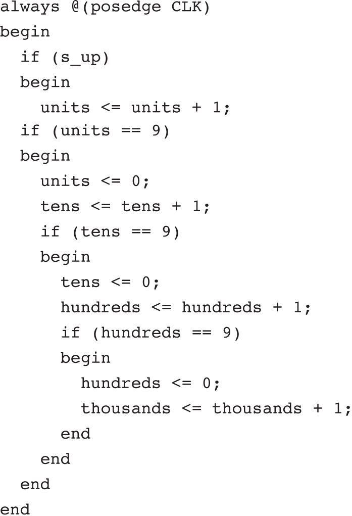
Most of the action takes place in the always
block. This checks to see if the debounced switch s_up
has been pressed. If it has, it adds one to units
. There then follows a sequence of ever deeper if
statements that check for the overflow of one digit and then increment the next digit and reset the current digit to 0 if this occurs:
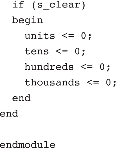
If the “Clear” switch is pressed, then all four digits are zeroed:
You will also need a UCF file. The one for Mojo is listed next. You will find suitable equivalents for the other boards in the downloads for this book.

There are several ways of getting source code for modules that you have created into a project. ISE occasionally gets confused about which files belong to it, and I have found the least problematic procedure for copying a module from another project (say debounce or decoder_7_seg in this example) is as follows:
1. Create the new project.
2. From your operating system’s file explorer, create a “src” directory inside the project directory.
3. Add copies of any module files that this project needs (debouncer.v and decoder_7_seg.v) into this “src” directory.
4. From ISE, use the option “Add Source…” and navigate to each of the .v files you just added to the “src” directory.
The “Design” tab in ISE shows you the relationship between the modules used in your project (Figure 5-6 ).

Figure 5-6 The modules used in the “counter_7_seg” project.
You can see in this hierarchical view that everything is correct, with the counter_7_seg module containing two debouncer modules and a display_7_seg module that itself contains a decoder_7_seg module. If you look closely, you can see that the counter_7_seg module has an icon next to it comprising three little squares in a triangular arrangement. This indicates that the counter_7_seg module is the top-level module of the project.
ISE will often work out for itself what the top-level module is, but sometimes it doesn’t, in which case you can specify that a particular module is the top-level module by right-clicking on it and specifying the option “Set As Top Module.”
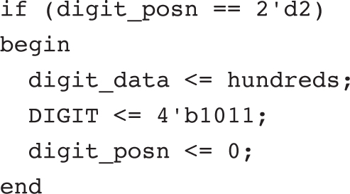
The Elbert 2 has only three digits rather than the four of the Mojo, so in most cases the differences in the Elbert version are simply reducing the number of digits from four to three. One effect of using three rather than four digits is that in display_7_seg
the digit_posn
counter needs to be manually reset to 0 after it reaches the hundreds digit:
Build the project and upload it onto your board. You will find that the number on the display will increment each time you press “Up” and reset to zero when you press the “Clear” button. You will need a lot of patience to test all four digits or even all three on the Elbert 2.
In this chapter, the potential of the FPGA is starting to reveal itself. In Chapter 6 , we will reuse the modules described in this chapter and go on to produce a realistic example of a countdown timer. The timer example also introduces a key concept in the design of FPGA systems called state machines .