2
Diode Circuits
2.1 The v‐i Characteristic of Diodes
Figure 2.1(a) shows the symbol for a diode, which allows an electric current (as a low resistance) in the forward direction, while blocking current (as a large resistance) in the reverse direction. Figure 2.1(b) shows the v‐i characteristic of a practical diode, which can be approximated by the Shockley diode equation (named after transistor coinventor William Bradford Shockley) or the diode law:

Figure 2.1 Symbol and v‐i characteristic of a diode.
where IS, η, and VT are the leakage (reverse saturation) current, the empirical constant (called the emission coefficient or ideality factor) between 1 and 2, and the thermal voltage, respectively.
Note that the thermal voltage VT is given by

2.1.1 Large‐Signal Diode Model for Switching Operations
When the signal applied to such electronic devices as diodes and transistors is large in comparison with the bias level, they show ON‐OFF behavior, functioning like a switch.
The v‐i characteristic curve of a diode in terms of its static behavior can be approximated by a solid/dotted piecewise linear (PWL) line for the forward‐/reverse‐bias mode as depicted in Figure 2.2(a). According to the approximation, the operation of a diode in the forward‐/reverse‐bias mode is represented by the equivalent model depicted in Figure 2.2(b).
2.1.2 Small‐Signal Diode Model for Amplifying Operations
Figure 2.3(a) and (b) shows the high‐frequency AC models of forward‐/reverse‐biased diodes, respectively. Note that the junction (or depletion or transition) capacitance defined as the ratio of the incremental change (Δqj) in the charge (in the depletion layer) to that (ΔvD) in the anode‐to‐cathode bias voltage vD can be expressed as

Figure 2.2 PWL approximation of the v‐i characteristic curve of a diode and the corresponding model.
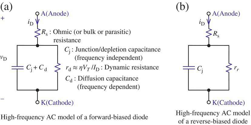
Figure 2.3 High‐frequency AC (small‐signal) model of a diode.

where M: junction gradient coefficient, Vj: (built‐in) junction potential with the value of 0.5∼0.9 V for a Si (silicon) diode and 0.2∼0.6 V for a Ge (germanium) diode, and Cj0: zero‐bias junction capacitance
Note also that the diffusion (or transit time) capacitance due to the diffusion of carriers from anode to cathode in the forward‐bias mode can be expressed as

where tT: transit or storage time taken for the charge to cross the diode, IQ: diode current at the operating point Q, η: emission coefficient or ideality factor, and, 
Note also that the dynamic resistance rd can be approximated as
2.2 Analysis/Simulation of Diode Circuits
The procedure of performing a large‐signal analysis for diode circuits can be summarized:
- Assume (guess) the ON/OFF state of each diode.
- For ON/OFF state, replace the diode by the forward‐/reverse‐bias model of each diode like the ones depicted in Figure 2.2(b).
- Solve the circuit and verify the result and the assumptions:
- For a diode assumed to be ON (with vD ≈ VTD), the initial guess is justified if iD > 0; otherwise, i.e. if iD < 0, resume the analysis with the assumption that the diode is OFF.
- For a diode assumed to be OFF (with iD = 0), the initial guess is justified if vD < VTD; otherwise, i.e. if vD ≥ VTD, resume the analysis with the assumption that the diode is ON.
2.2.1 Examples of Diode Circuits
See the following examples.
Example 2.2 Analysis of a Two‐Diode Circuit Using CVD (Constant Voltage Drop) Model
For the circuit of Figure 2.5(a), replace the diodes (assumed to be ON) by the CVD model (that is, the PWL model with rf = 0 Ω and VTD = 0.7 V) and find the voltages v1 and v2. Compare them and those obtained using the exponential model (Eq. 2.1.1) with Is = 10 × 10−15 A and ηVT = 25.9 mV.
Note that there are four possible states for the two diodes D1 and D2: ON‐ON, ON‐OFF, OFF‐ON, and OFF‐OFF. First, assuming that both D1 and D2 are ON, we replace them by the Constant Voltage Drop (CVD) model to draw the equivalent as shown in Figure 2.5(b). Then the voltages v1 and v2 can easily be found as

yielding


Figure 2.5 A two‐diode circuit for Example 2.2.
However,  = −0.27 mA < 0 contradicts the assumption that D1 is ON. That is why we make another assumption that D1 and D2 are ON and OFF, respectively, draw the corresponding equivalent as depicted in Figure 2.5(c) and get

Still,  = 6.7 V > 0 contradicts the assumption that D2 is OFF. That is why we make another assumption that D1 and D2 are OFF and ON, respectively, draw the corresponding equivalent as depicted in Figure 2.5(d) and get

This yields  = v1 = −0.2 V < 0 and
  = i = 1.02 mA > 0, suiting the assumption that D1 and D2 are OFF and ON, respectively. Therefore, the solution is v1 = −0.2 V and v2 = v1 − 0.7 = −0.9 V.
If we use the (nonlinear) exponential model (2.1.1) for a more exact analysis, KCL can be applied at nodes 1 and 2 to yield a set of two node equations in v1 and v2 as
where Eq. (2.1.1a) has been used to express diode current iD in terms of diode voltage vD. To solve this set of nonlinear equations, the MATLAB function ‘fsolve()’ can be used as listed in the following script “elec02e02.m”:
%elec02e02.mIs=10e-15; nVT=0.0259; % Diode exponential model parametersVs1=10; Vs2=-6; R1=1e4; R2=5e3; % Circuit parameter valuesiD = @(vD)Is*(exp(vD/nVT)-1); % Eq. (2.2.1a)eqs = @(v)[(Vs1-v(1))/R1-iD(v(1))-iD(v(1)-v(2));iD(v(1)-v(2))-(v(2)-Vs2)/R2]; % Eq. (E2.2.5)v = fsolve(eqs,[1 1]), ID2=iD(v(1)-v(2))
Running this script yields the following, which is close to the above result with the CVD model:
v = -0.2289 -0.8855, ID2 = 0.0010
2.2.2 Clipper/Clamper Circuits
Figure 2.6(a1) and (a2) respectively show clipper circuits for clipping the upper and lower portion of the input signal above/below the reference level of (V1 + VD)/(−V2 −VD), which is determined by the DC voltage source connected in series with the diode. Figure 2.6(b1) and (b2) show their input and output voltage waveforms obtained from PSpice simulation. Running the following MATLAB script yields a similar result.


Figure 2.6 Clipper circuits to clip the upper/lower portion of the input signal and their input/output signals.
%elec02f06_1_clipper.mIs=10e-15; nVT=0.0259; VD=0.7;iD=@(vD)Is*(exp(vD/nVT)-1); % Eq. (2.2.1a)t=[0:0.01:2.5]; vi=10*sin(2*pi*t); R=1e3; V1=5;v10=0; Nt=length(t); options=optimoptions ('fsolve','Display','none');for n=1:Nteq = @(v)vi(n)-v-R*iD(v-V1); % KCL equation in vif n>1, v10=v(n-1); end; v(n)=fsolve(eq,v10,options);endplot(t,vi,'r:', t,v,'g', t,V1+VD,'k:')
Figure 2.6(a3) shows a two‐level clipper circuit, which combines two clipper circuits for clipping the upper and lower portions of the input signal so that the output voltage can be kept within the range of [−V2 −VD, V1+VD]. Figure 2.6(b3) shows its input and output voltage waveforms.
Figure 2.7(a1) and (a2) shows positive/negative clamper circuits (called clamped capacitors or DC restorers), which push the input signal (within [Vi,min, Vi,max]) upward/downward by the positive/negative capacitor voltage charged (when vi = Vi,min/Vi,max), i.e. VC = (−Vi,min + Vr −VD)/(Vi,max −Vr −VD) so that their outputs are related with their inputs as
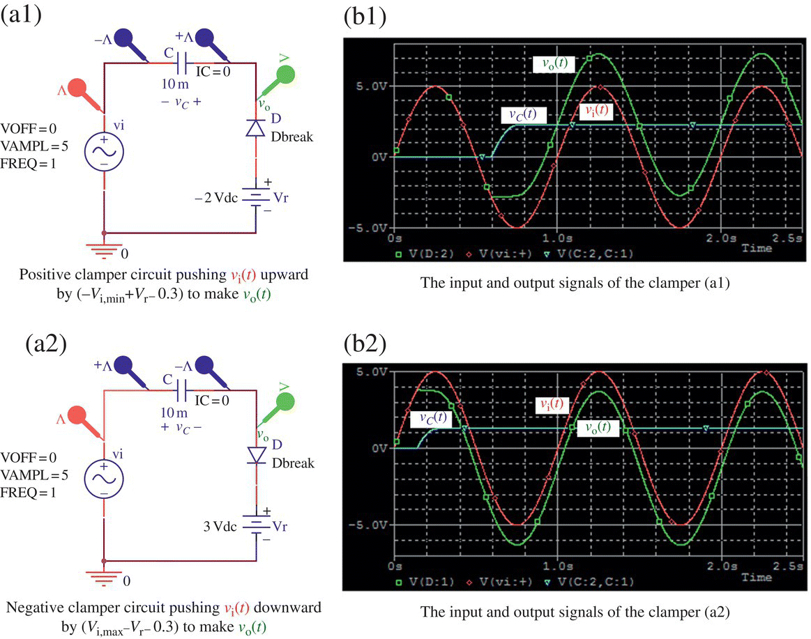
Figure 2.7 Positive/negative clamper circuits and their input/output signal waveforms (“clipper_clamper.opj”).
Note that the trough/peak level of the positive/negative clamper outputs will be (Vr −VD)/(Vr+VD), respectively, where VD depends on the capacitance C and how long C has been charged.
2.2.3 Half‐wave Rectifier
The diode in the circuit of Figure 2.8(a) can be represented by the CVD model as shown in Figure 2.8(b), which is valid in the forward mode of the diode, i.e. while vi ≥ Vos where the offset or cut‐in voltage Vos (slightly less than the threshold voltage VTD) is the diode voltage at which the diode starts to turn on. Here, we can find the cut‐in or ignition angle ϕ at which the diode starts to turn on:

Similarly, the extinction angle at the end of the (first) positive half‐cycle is π − ϕ (see Figure 2.8(c)). Note that the peak inverse voltage (PIV) of the diode is Vm.
2.2.4 Half‐wave Rectifier with Capacitor – Peak Rectifier
Figure 2.9.1(a) shows the PSpice schematic of a half‐wave rectifier composed of a diode, a capacitor, and a resistor, called a peak rectifier, which conducts in the forward direction for vD ≥ VTD = 0.65 V. Figure 2.9.1(b) and (c) shows the equivalent circuits of the rectifier for vi ≥ vo+VTD and vi < vo+VTD, respectively. Figure 2.9.1(d) shows the PSpice simulation result obtained from the Transient Analysis with Run_to_time of 40 ms. From this PSpice simulation result, we find the upper/lower limit VH/VL of the output voltage vo(t) and the rising/falling period TR/TF as

Figure 2.8 A half‐wave rectifier and its input/output voltage waveforms.
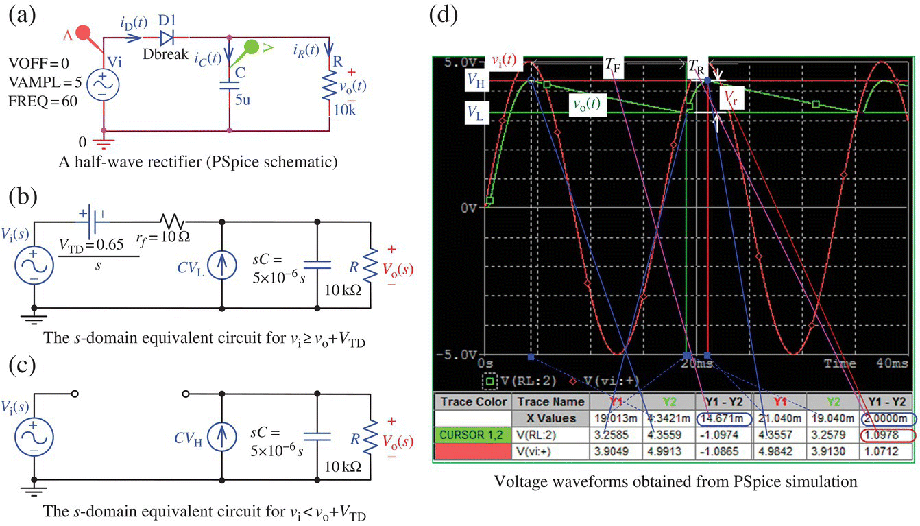
Figure 2.9.1 Equivalent circuits and input/output voltage waveforms of a half‐wave rectifier (“rectifier_halfwave.opj”).

To obtain these parameters, after getting the output voltage waveform in the PSpice A/D (Probe) window, click the Toggle Cursor button on the toolbar to activate the two cross‐type cursors on the graph. Then use the left/right mouse button and/or arrow/shift‐arrow key or click the appropriate toolbar button to move them to the peak/trough and read their coordinates from the Probe Cursor box. If you have two or more waveforms on the Probe window, you can choose one which you want to take a close look at by clicking the name of the corresponding variable under the graph.
To get the upper/lower limit VH/VL of the output voltage vo(t) and the rising/falling period TR/TF via an analytical approach using MATLAB, we set up the following equations:
Noting that VH is already known as VH = Vm − VTD = 5 − 0.65 = 4.35, we solve this set of equations to find VL = 3.23, TR = 0.0018, and TF = 0.0149 by saving these equations into an M‐file named, say, ‘halfwave_rectifier_eq.m’ and running the following MATLAB script “do_halfwave_rectifier.m.”
%do_halfwave_rectifier.mclearglobal Vm f VTDVm=5; f=60; VTD=0.65;VH=Vm-VTD; % Local maximum (High Voltage) of vo(t)R=1e4; C=5e-6;x0=[0 0 0]; % Initial guess of [VL TR TF]% VL: Low Voltage (Local Min) of vo(t), TR: Rise Time, TF: Falling Timex=fsolve('halfwave_rectifier_eq',x0,optimoptions ('fsolve'),C,R)VL=x(1); TR=x(2); TF=x(3);fprintf('\n VH=%8.4f, VL=%8.4f, TR=%8.4f, TF=%8.4f\n', VH,VL,TR,TF)function y=halfwave_rectifier_eq(x,C,R)global Vm f VTDVH=Vm-VTD; w=2*pi*f; T=1/f;VL=x(1); TR=x(2); TF=x(3);y=[VH*exp(-TF/R/C)-VL; % Eq. (2.2.3a)VH-VL-Vm*(1-cos(w*TR)); % Eq. (2.2.3b)TR+TF-T]; % Eq. (2.2.3c)
Now, to perform the MATLAB simulation of the rectifier circuit with capacitor filter in Figure 2.9.1(a), we discretize the integro‐differential equation for the voltage‐current relationship (VCR) of the capacitor as
where
The numerical solution process to find the output voltage of a half‐wave rectifier as shown in Figure 2.9.1(a) has been cast into the following MATLAB function ‘rectifier_RC()’. The following MATLAB script “elec02f09.m” uses this function to find vo(t) of the half‐wave rectifier (in Figure 2.9.1(a)) as Figure 2.9.2 together with the values of VH = 4.36, VL = 3.26, TR = 0.002, and TF = 0.0147.
function [vo,vD,iD,iR]=rectifier_RC(vit,R,C,Is,nVT)% vit = [vi; t]: 2-row matrix consisting of the input signal and time% R,C = Resistance and Capacitance% Copyleft: Won Y. Yang, wyyang53@hanmail.net, CAU for academic use onlyif nargin<5, nVT=(273+27)/11605; end % Thermal voltageiDv = @(vD)Is*(exp(vD/nVT)-1); % Eq. (2.1.1a)[Nr,Nc]=size(vit);if Nc==2, vi=vit(:,1); ts=vit(:,2); N=Nr;elseif Nr==2, vi=vit(1,:); ts=vit(2,:); N=Nc;enddt=ts(2)-ts(1); % Sampling intervalvo(1) = 0; % Initial value of the output voltage vo(t)for n=1:NvD(n) = vi(n)-vo(n); iD(n) = iDv(vD(n)); iR(n) = vo(n)/R;iC(n) = iD(n) - iR(n); % Eq. (2.2.4b)vo(n+1) = vo(n) + iC(n)/C*dt; % Eq. (2.2.4a)endvo = vo(2:end); % To make the size of vo equal to that of vi%elec02f09.m% To simulate the rectifier in Fig. 2.9.1(a)clear, clfVm=5; f=60; w=2*pi*f; P=1/f; % Amplitude, Frequency, Period of vi(t)R=1e4; C=5e-6; % Values of R and C of the RC filterdt=1e-5; t=0:dt:0.04; vi=Vm*sin(w*t); % Time range, Input voltage vi(t)Is=1e-14; % Saturation currentvo=rectifier_RC([vi; t],R,C,Is);subplot(313), plot(t,vi,'g', t,vo,'r')N1=floor(P/dt); nn0=1:N1;[VH,imax]=max(vo(nn0)); VH % The 1st peak value of vo(t)tH1=t(imax); % The 1st peak timeN2=2*N1+10; nn1=N1:N2;[VL,imin]=min(abs(vo(nn1))); VLtL1=t(N1-1+imin); % The 1st valley time[emin,imin]=min(abs(vo(nn1)-VH));tH2=t(N1-1+imin); % The 2nd peak timeTF=tL1-tH1, TR=tH2-tL1 % Falling/Rising period
>>elec02f09VH = 4.3567 % Upper limit (High value) of the output voltageVL = 3.2586 % Lower limit (Low value) of the output voltageTF = 0.0147 % Falling timeTR = 0.0020 % Rising time
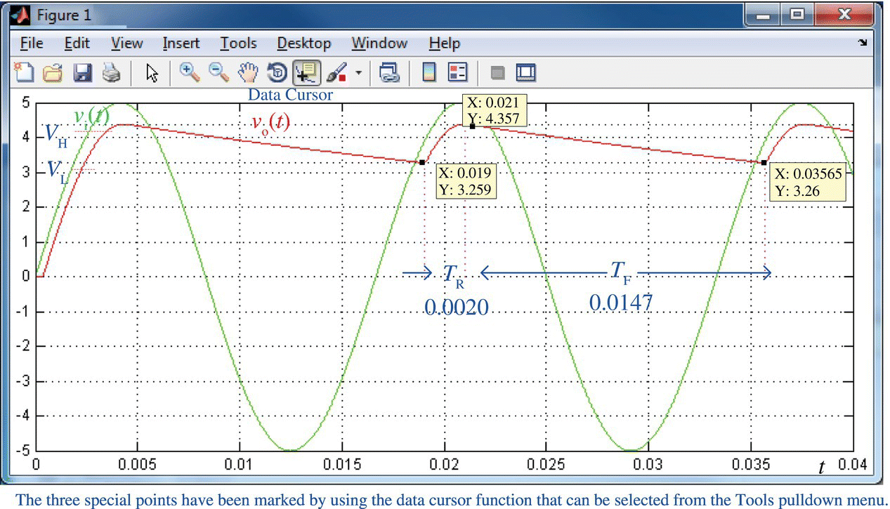
Figure 2.9.2 Input/output voltage waveforms of the half‐wave rectifier.
These results are close to those obtained via an analytical approach or the PSpice simulation results depicted in Figure 2.9.1(d).
One observation about the behavior of the output voltage vo(t) made from Figures 2.9.1(d) or 2.9.2 is that vo(t) follows the input voltage vi(t) = Vmsin (ωt) = 5 sin (2πft) (f = 60 Hz) promptly when rising up, but very lazily when falling down, which is helpful for making the rectifier output vo(t) smooth with a small ripple. Why are the behaviors of the circuit different for the two cases of the capacitor being charged and discharged? It is because the time constant of the circuit with the capacitor being charged (via the diode) from the source is much shorter than that with the diode off and the capacitor being discharged, as can be seen from the equivalent circuits with the diode ON/OFF depicted in Figure 2.9.1(b) and (c):


(cf.) This kind of circuits can be used not only for rectifying and smoothing an AC voltage into a DC voltage in power supplies, but also for demodulating a conventional amplitude modulated (AM) signal to restore the message signal in communication systems.
2.2.5 Full‐wave Rectifier
Figure 2.10(a1) and (a2) shows a full‐wave rectifier using a center‐tapped transformer and another full‐wave rectifier using a diode bridge, respectively.

Figure 2.10 Two full‐wave rectifiers and their voltage transfer characteristics (VTCs), output voltage waveforms, and peak inverse voltages (PIVs).
Figure 2.10(b1) and (b2) shows their input‐output relationships, called voltage transfer characteristic (VTC):


Figure 2.10(c1) and (c2) shows their PSpice simulation results (obtained from the Transient analysis with vi(t) = Vm sin (2πt) (Vm = 5 V)) for the output voltage vo(t) and a reversed diode voltage −vD(t), from which we see their PIVs for a diode as


2.2.6 Full‐wave Rectifier with LC Filter
Figure 2.11(a) shows the PSpice schematic of a rectifier circuit in which a full‐wave rectified voltage vi(t) = |10 sin (2π60t)| is made smooth by an LC low‐pass filter as can be observed from the input and output signals and their spectra in Figure 2.11(b) and (c), respectively. We are going to find the condition on LC (with R = 10 kΩ) that should be satisfied to keep the relative magnitude of the major harmonic component to the DC component less than rmax, say, 5%. To this end, we will perform the Fourier analysis to find the two leading frequency components (including the DC term) of the input vi(t) and output vo(t).
Since the input voltage vi(t) to the LC filter is a full‐wave rectified cosine wave, we can use (E1.5.7) (in Example 1.5) to write its Fourier series representation as

Figure 2.11 PSpice simulation of a full‐wave rectifier (“rectifier_fullwave.opj”).

The transfer function and frequency response of the LCR filter are

Thus, the magnitudes of the DC component and the first harmonic in the output are


Consequently, we can write the condition on LC (with R = 10 kΩ) for the relative magnitude of the major harmonic to the DC component to be less than rmax as
It seems to be good to determine the admissible region for (C, L) satisfying the design specification on filtering off harmonics with rmax = 5 and 10%. This can be done by saving Eq. (2.2.11) in an M‐file named ‘elec02f12_f.m’ and running the following MATLAB script “elec02f12.m” that uses the nonlinear equation solver ‘fsolve()’ to solve Eq. (2.2.11) for L at different values of C in some range and plot the C-L curves for rmax = 5 and 10% as shown in Figure 2.12. Note that the region below the curves in Figure 2.12 is not admissible in the sense that no positive values of (C, L) in the region can satisfy the above inequality constraint (2.2.11).
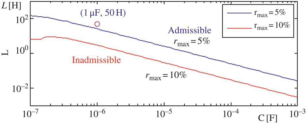
Figure 2.12 Admissible region for (C, L) to satisfy the design specification on the relative magnitude of the major harmonic to the DC component.
%elec02f12.mclear, clfglobal R w0R=1e4; w0=2*pi*60;CC=logspace(-7,-3,100); % Range of C to 100 points on [10^-7,10^-3]ftn='elec02f12_f'; gss='brgm'; % The function to solveratioms=[0.05 1];for i=1:numel(ratioms)for m=1:length(CC)C= CC(m); % Given the value of Cif m<2, L0=10; else L0=LL(m-1); end % Initial guess of LLL(m)= fsolve(ftn,L0,optimset('Display','off'),C,ratioms(i));endloglog(CC,LL,gss(i)), hold onendplot(1e-6,50,'mo'); axis([CC([1 end]) 1e-3 1e3]);xlabel('C'); ylabel('L')function y=elec02f12_f(L,C,r_max)global R w0w=2*w0; y= (1-w^2*L*C)^2 + (w*L/R)^2 - (2/3/r_max)^2; % Eq. (2.2.11)
2.2.7 Precision Rectifiers
Figure 2.13(a) shows a basic precision half‐wave rectifier circuit, which consists of an OP amp (having a diode in its negative‐feedback path) and a resistor where the OP amp output voltage vo0 is basically determined as A(v+ − v−) = A(vi − v−) (A: the open‐loop gain) unless it exceeds the saturation voltage ±Vom (Eq. (5.1.1) in Section 5.1). How will it work? Let us assume that the diode is off so that no current flows through R and thus v− = 0.
Case 1
When vi = v+ > 0,
vo0 will go positive to make vD = vo0 − v− > 0 so that the forward‐biased diode will conduct. This will make a closed feedback path between the output and the negative input terminal of the OP amp so that by the virtual short principle (Remark 5.1),
Case 2
When vi = v+ < 0,
vo0 will go negative to make vD = vo0 − v− < 0 so that the reverse‐biased diode will be cut off. Thus, no current will flow through R, causing
where the negative feedback is broken up so that the output voltage vo0 of the OP amp operating in the open‐loop mode will go to the negative saturation voltage −Vom.
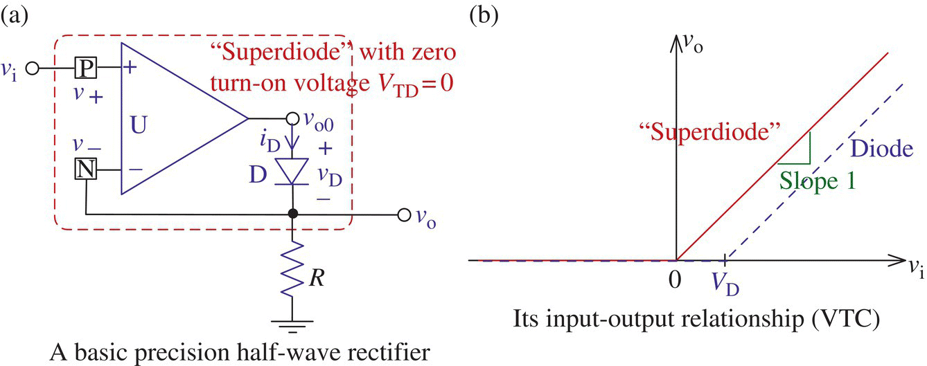
Figure 2.13 The basic precision half‐wave rectifier, called a “superdiode.”
Figure 2.13(b) shows the input-output relationship (solid line), called VTC, of the half‐wave rectifier circuit based on Eq. (2.2.12a,b). Note that it does not have the threshold voltage VD unlike that (dotted line) of the simple half‐wave rectifier circuit in Figure 2.8(a) and that is why such a combination of a diode with an OP amp may well be called a “superdiode” with VD = 0. Isn't it marvelous? Now, let us see some improved versions of this basic precision rectifier.
2.2.7.1 Improved Precision Half‐wave Rectifier
Figure 2.14(a) shows an improved precision half‐wave rectifier circuit. Let us see how it works.
Case 1
When vi > 0,
vo0 (desiring to be A(v+ − v−) ~ −Avi) will go negative to make  = v− − vo0 > 0 so that the forward‐biased diode D1 will conduct. This will make a closed feedback path via D1 between the output and the negative input terminal of the OP amp so that by the virtual short principle, v− ≈ v+ = 0 V (virtual ground) and thus vo0 = v− −
  = v− − VD = −VD (clamped at one diode drop below zero), keeping D2 off. Then no current flows through R2 so that
Case 2
When vi < 0,
vo0 will be positive to forward bias D2 (through R2-R1-vi) and reverse bias D1 (with  ) so that D1/D2 will be off/on, respectively. Then a negative feedback path is established through D2-R2 so that by the virtual short principle, v‐ ≈ v+ = 0 V and thus
This causes  so that the reverse‐biased D1 can be kept off. Note that whether vi > 0 or vi < 0, a negative feedback path is maintained so that time required to bring the OP amp out of saturation (when the sign of vi changes from – to +) can be saved.
Figure 2.14(b) shows the input-output relationship, called VTC, of the half‐wave rectifier circuit based on Eqs. (2.2.13a) and (2.2.13b). The PSpice simulation results (obtained from the Transient analysis with vi(t) = Vm sin (2πt) (Vm = 5 V)) of the two precision half‐wave rectifiers in Figures 2.13(a) and 2.14(a) for the output voltage vo(t) and a reversed diode voltage −vD(t) are shown in Figure 2.15(a) and (b). From the graphs, we see their PIVs for a diode as
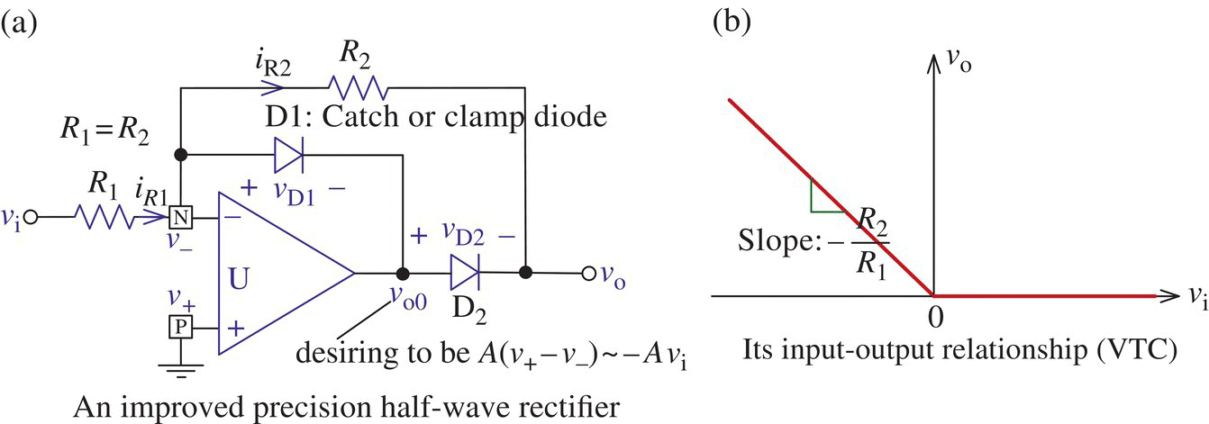
Figure 2.14 An improved (fast) precision half‐wave rectifier.

Figure 2.15 Simulation results of two precision half‐wave rectifiers (“elec02f15a.opj,” “elec02f15b.opj”).


where Vm and Vom are the maxima of the input voltage vi(t) and OP amp output voltage vo0(t), respectively.
2.2.7.2 Precision Full‐wave Rectifier
Figure 2.16.1(a) shows a precision full‐wave rectifier circuit, which consists of a precision half‐wave rectifier, called a “superdiode” (Figure 2.13(a)), in the upper part and another precision half‐wave rectifier with an inverting OP amp circuit (Figure 2.14(a)) in the lower part. When vi = v+1 > 0, the upper part lets the input vi pass and when vi = v−2 < 0, the lower part inverts the input vi with gain −R2/R1 (see Eq. (6.2.8)). Therefore, as shown in Figure 2.16.1(b), the VTC of this rectifier is
Figure 2.16.2(a) shows another precision full‐wave rectifier circuit, which consists of a “superdiode” (Figure 2.13(a)) (with an additional capacitor C in parallel with diode D1) in the left part and an inverting OP amp circuit (with diode D1 connected to its positive input terminal) in the right part. Note that the two OP amps U1/U2 have negative feedback through C/R2 so that by the virtual short principle, we always have v−1 ≈ v+1 = vi and v−2 ≈ v+2. Let us see how it works:
Case 1
When vi = v+1 > 0,
vo1 (desiring to be A(v+1 − v−1)) will be high enough to make D1 off (with  = v−1 − vo1 < VTD) and D2 on (with
  = vo1 − v
+2 = VD) so that vo will be

where no current flows through R1‐R2 since C as well as D1 will not conduct once it has instantly been charged to vC = v−1 − vo1 = v+2 − vo1 = − = −VD.

Figure 2.16.1 A precision full‐wave rectifier.
Case 2
When vi = v+1 ≈ v−1 < 0,
vo1 will be low enough to make D1 on (with  = v−1 − vo1 = VD) and D2 off (with
  = vo1 − v
+2 < VTD) so that iR3 = 0 and thus v−2 ≈ v+2 =R3iR3 = 0. Then the OP amp U2 together with R1 and R2 functions as an inverting amplifier with gain −R2/R1 (see Eq. (5.2.8)) so that

where C as well as D2 will not conduct once it has instantly been charged to vC =  = VD.
= VD.
Therefore, the VTC of this rectifier can also be described by Eq. (2.2.15) or Figure 2.16.2(b), which is identical to Figure 2.16.1(b).
How do the two precision full‐wave rectifiers compare with? First, the input impedance (seen from vi) of the latter is much larger than that (R1) of the former. Second, the PIVs of D1 and D2 in the latter (where the OP amps never enter the saturation region) are Vm + VD in common, while those in the former (where the OP amps enter the negative saturation region when the diode in their negative feedback paths is off) are as high as max{−vDi(t)} = Vm + Vom in common where Vm and Vom are the maxima of the input voltage vi(t) and OP amp output voltage vo0(t), respectively. From the PSpice simulation results shown in Figure 2.17, we see that the PIVs of the diodes in the two rectifiers are


Figure 2.16.2 A precision full‐wave rectifier with high input impedance [E-2, J-2, W-8].

Figure 2.17 PSpice simulation of the two precision full‐wave rectifiers (“elec02f17_1.opj,” ”elec02f17_2.opj”).
2.2.8 Small‐Signal (AC) Analysis of Diode Circuits
Consider the circuit with the PSpice schematic of Figure 2.18.1(a) where the PSpice Model for the diode D1N4148 (opened by selecting the diode and clicking on Edit>PSpice Model from the top menu bar) is shown in Figure 2.18.1(b). For PSpice simulation with the schematic, we do the following:
- Fill in the Simulation Settings dialog box (for Transient or Bias_Point analysis) as shown in Figure 2.18.1(c) and click OK to close the dialog box.
- Place a Current Marker to measure the diode current iD(t) and click Run to get the waveform of iD(t) as shown in Figure 2.18.1(d) or the bias point analysis on the schematic or in the output file.
To get the v-i characteristic of the diode and draw the load lines in the PSpice A/D Window, we do the following:
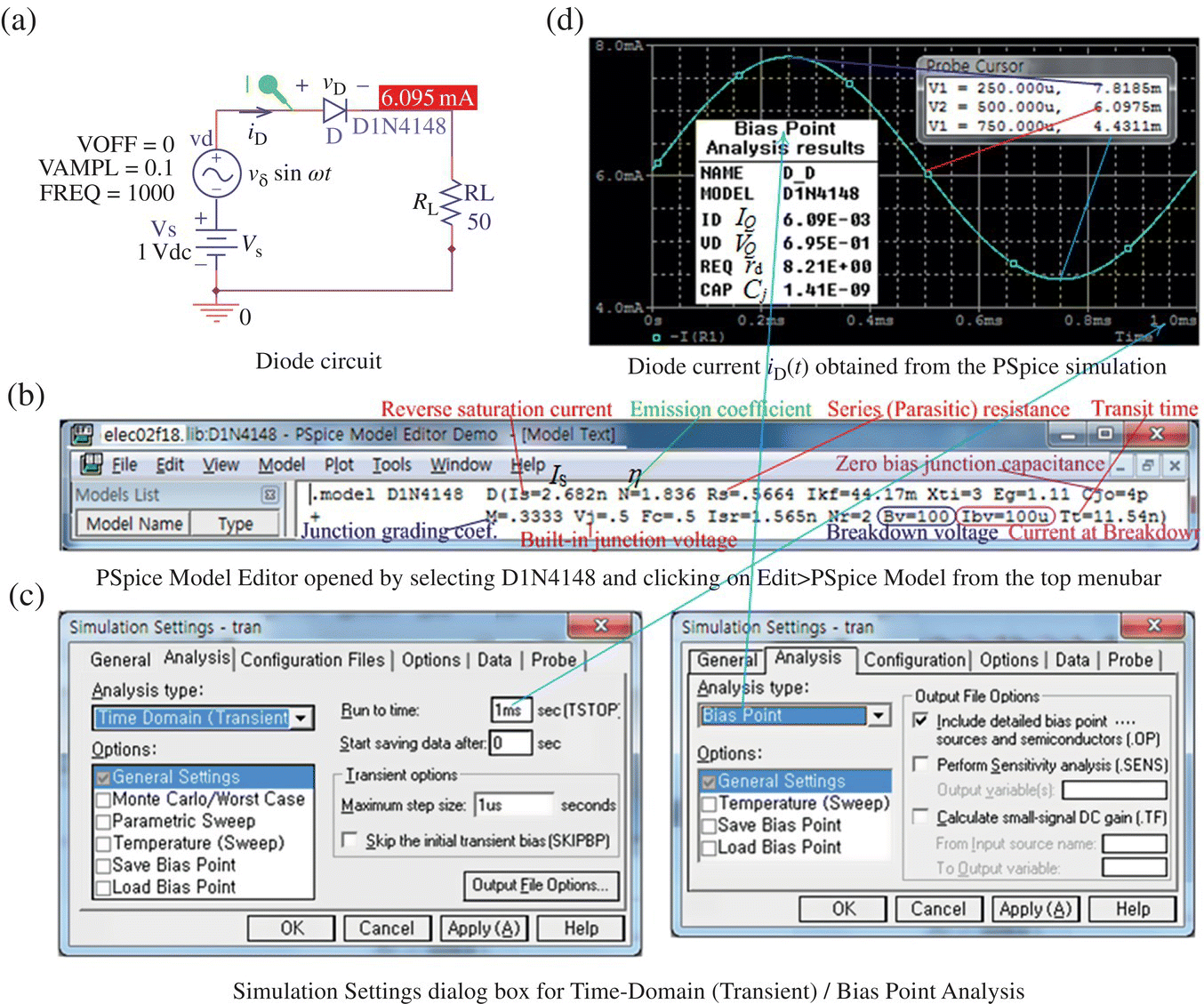
Figure 2.18.1 Simulation of a diode circuit driven by a DC source and an AC source (“e lec02f18.opj”).
- Construct the PSpice schematic as Figure 2.18.2(a)
- Fill in the Simulation Settings dialog box for DC Sweep analysis (Figure 2.18.2(b)) and click Run.
- Click Trace>Add Trace from the top menu bar to open the Add Traces dialog box and fill in the box as Figure 2.18.2(e), which yields the load lines (Figure 2.18.2(c)).
- (Q) Can the waveform of iD(t) (Figure 2.18.1(d)) be predicted from the Q‐points in Figure 2.18.2(c)?
To determine the diode constants of the diode D1N1418, we can use the curve fitting toolbox ‘cftool’ (in MATLAB) to fit the data points (vD, iD) of the v-i characteristic curve (Figure 2.18.2(c)) to the Shockley diode equation. Noting that curve fitting works better for linear functions than for nonlinear functions, let us approximate the Shockley diode equation and take the logarithms of both sides to linearize as
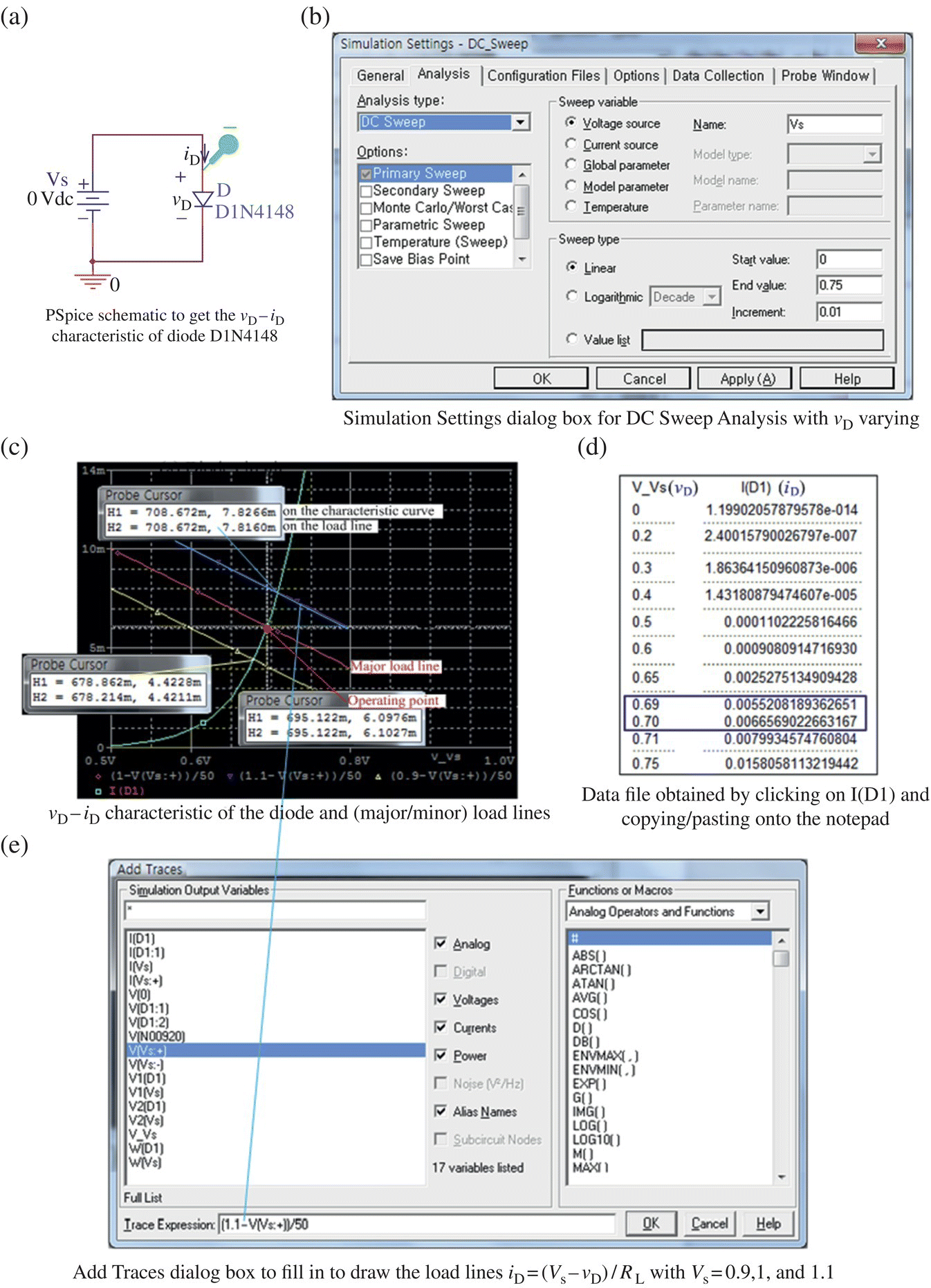
Figure 2.18.2 PSpice simulation to get the v-i characteristic and operating point(s) for (“elec02f18b.opj”).
To determine the parameters 1/ηVT and ln IS of Eq. (2.2.18) which fit the PSpice simulation data, do the following:
- Select I(D1) below the current waveform graph (Figure 2.18.2(c)), press ‘CTRL+c’ (copy), and then press ‘CTRL+v’ (paste) into a notepad to create a data file named ‘vD_iD.dat’ (Figure 2.18.2(d)) where the first line containing the variable descriptions should be deleted.
- Run the following MATLAB statements:
>>load vD_iD.dat, vD=vD_iD(:,1); iD=vD_iD(:,2);ln_iD=log(iD); % Take natural logarithm to linearize fitting ftncftool % To start the curve fitting toolbox
This will open the CFTOOL window as shown in Figure 2.18.3(a).
- Click
 button to open the Data dialog box (Figure 2.18.3(b)).
 - In the Data dialog box, put ‘vD’ and ‘ln_iD’ into the fields of X Data and Y Data, respectively, and click
 button to create a new data set named ‘ln_iD vs. vD’.
 - Click
 button to open the Fitting dialog box (Figure 2.18.3(c)).
 - In the Fitting dialog box, select ‘ln_iD vs. vD’ and ‘Custom Equations’ in the fields of Data set and Type of fit, respectively.
- Click
 button inside Custom Equations panel to open a New Custom Equation dialog box.
 - In the New Custom Equation dialog box, click the tab
General Equations and construct the model equation corresponding Eq. (2.2.18) as
y = a*x +ln_Iswhere a and ln_Is stand for 1/ηVT and ln IS, respectively. Then click
 button to close the New Custom Equation dialog box.
 - In the Fitting dialog box, click
 button to make the following results appear in the box below
Result:

Figure 2.18.3 Using cftool for curve fitting to determine the diode constants.
Coefficients (with 95% confidence bounds):a = 21.24 (20.87, 21.6)ln_Is = -19.72 (-19.88, -19.56)
This implies that the parameters ηVT and IS have been determined as

where the true values of ηVT and IS can be found from the PSpice Model of the diode (Figure 2.18.1(b)) as
- (Q) Are the curve fitting results fine? To be honest with our readers, the accuracy of curve fitting depends on not only the number of measured data points but also the data range.
With the diode constants found in the corresponding PSpice Model Editor (Figure 2.18.1(b)) or obtained from the curve fitting (Figure 2.18.1(c)), let us make a theoretical analysis of the diode circuit (Figure 2.18.1(a)) by using the nonlinear equation solver ‘fsolve()’ of MATLAB to solve the (nonlinear) KCL equation
for vD(t) or to solve the (nonlinear) KVL equation
for iD(t). To do this job, we compose the MATLAB script “elec02f1804.m” as below and run it to get Figure 2.18.4, which shows the diode current waveform (plotted as blue line) together with those obtained from the PSpice simulation (Figure 2.18.1(d)) and the theoretical analysis.
(Q) How would you copy the PSpice simulation data (Figure 2.18.1(d)) into a MATLAB graph?
%elec02f1804.mVs=1; vd=0.1; % Amplitudes of DC/AC voltage sourcesRL=50; % Load resistancef=1000; w=2*pi*f; % Frequency of the AC sourceIs=2.682e-9; nVT=0.0475; % Diode constants Eq. (2.2.20)dt=1e-6; t=[0:1000]*dt; % Time range for solutionvst = Vs + vd*sin(w*t); % Source voltage waveform% To solve Eq. (2.2.21) for vD and use Eq. (2.1.1) to find iD(t) from vD(t)eq_2221=@(vD,Is,nVT,RL,vs)RL*Is*(exp(vD/nVT)-1)-vs+vD; % Eq. (2.2.21)options=optimset('Display','off');for n=1:length(t)vD0=0.7; vD(n)=fsolve(eq_2221,vD0,options,Is,nVT,RL,vst(n));iD(n)=Is*(exp(vD(n)/nVT)-1);end% To solve Eq. (2.2.22) for iD(t)eq_2222=@(iD,Is,nVT,RL,vs)vs-nVT*log(iD/Is+1)-RL*iD; % Eq. (2.2.22)for n=1:length(t)iD0=0.006; iD1(n)=fsolve(eq_2222,iD0,options,Is,nVT,RL,vst(n));endload t_iD.dat % iD(t) data from PSpicet_PSpice=t_iD(:,1); iD_PSpice=t_iD(:,2);VQ=695e-3; IQ=6.1e-3; % Operating point from Fig. 2.18.2(c)% To find the dynamic distance rddvD=0.7-0.69; diD=0.00665690237656236-0.00552081875503063;rd1=dvD/diD % Eq. (2.2.23a) using PSpice data in data file 'vD_iD.dat'rd2=nVT/(Is+IQ) % Eq. (2.2.23b) using the Shockley diode equationrd0=8.21; % from the output file obtained from Bias Point analysis% To find iD(t) using the analytical expression Eq. (1.1.12)iD2 = IQ+vd/(RL+rd0)*sin(w*t); % Eq. (1.1.12)plot(t,iD, t,iD1,'m:', t_PSpice,iD_PSpice,'g', t,iD2,'r'), grid on, shglegend('fsolve vD-iD','fsolve iD-vD','PSpice','Eq. (1.1.12) with rd0')
Now, to get an overview of the input-output relationship of the diode circuit, let us perform a (theoretical) small‐signal analysis by using Eqs. (1.1.12) and (1.1.13). First, we get the operating point Q as (VQ, IQ) = (0.695, 0.0061) from the intersection of the (major) load line and the v-i characteristic curve in Figure 2.18.2(c). Then, we find the dynamic resistance rd by reading REQ = 8.21 from the Bias Point analysis result shown in the output file (Figure 2.18.1(d)) or by using the PSpice data (stored in the data file ‘vD_iD.dat’) or Eq. (2.1.5) as follows:

Figure 2.18.4 Diode current waveforms obtained in various ways.
Which one of the three values [8.21 (from PSpice Bias Point analysis), 8.80 (from PSpice simulation data), 7.79 (from the theoretical formula)] should we use for Eqs. (1.1.12) and (1.1.13)? The authors have no idea. How about 8.21 close to their average? Thus, we use Eqs. (1.1.12) and (11.13) with rd = 8.21 to write the theoretical equation for the diode currents/voltages as


This diode current waveform with rd = 8.21 is depicted together with the ones obtained in other ways in Figure 2.18.4. The diode current waveforms are expected to become closer to each other if the magnitude vδ of AC voltage is smaller so that the approximation of the v-i characteristic curve by its tangent line at Q‐point can become more accurate.
2.3 Zender Diodes
Figure 2.19(a) and (b) shows the symbol and the v-i characteristic for a special kind of diode, called a Zener diode where vZ = −vD and iZ = −iD. A Zener diode behaves as other normal diodes in the forward‐bias mode but, in the reverse‐bias mode, withstands the reverse diode current (up to IZ,max) while keeping vZ = −vD close to the Zener (breakdown) voltage VZ (even with some variation in its current iD) as long as iZ = −iD remains between IZ,min and IZ,max. The maximum reverse current IZ,max that the diode can endure is PZ,max/VZ where PZ,max is the maximum power dissipation. The minimum reverse current IZ,min needed to keep the diode in the reverse breakdown mode is slightly below the Zener knee current IZK, at which the diode exhibits the reverse breakdown. The v-i characteristic curve of a Zener diode in terms of its static behavior can be approximated by a red/brown PWL line for the forward‐/reverse‐bias mode as depicted in Figure 2.19(b) where the diode resistance rf (in the forward‐bias mode) and the Zener resistance rz (in the reverse‐bias mode) are defined as
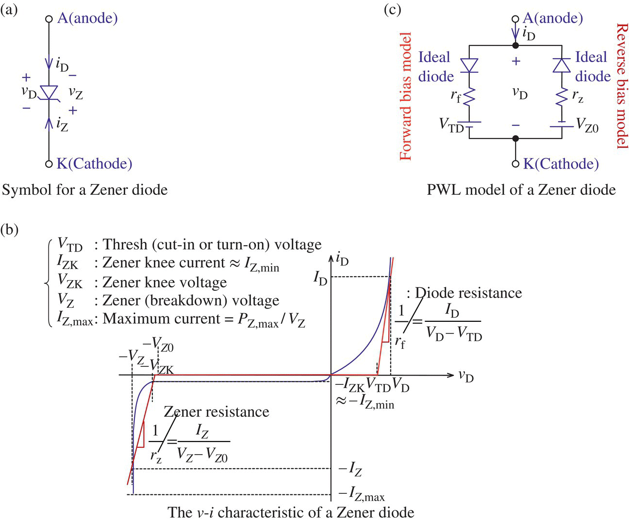
Figure 2.19 Symbol, v-i characteristic, and PWL model of a Zener diode.

Here, −VZ0 is the diode voltage at the intersection of the straight line having slope 1/rz with the voltage axis and it is almost equal to the Zener knee voltage −VZK. According to the approximation, the v-i characteristic of a Zener diode in the forward‐/reverse‐bias mode is represented by the equivalent model depicted in Figure 2.19(c).
Figure 2.20(a) shows a Zener (shunt) regulator, which is supposed to maintain an almost constant output voltage for all the variation of the DC voltage source vs and the load resistor RL. In order for the regulator to function properly in the breakdown region, the Zener diode current iZ should be bounded as

Thus, the source resistance Rs should satisfy the following inequality:
If IZ,max = PZ,max/VZ has not yet been specified, Rs can be set to some value slightly less than the upper bound of Inequality (2.3.3):

Figure 2.20 Zener (shunt) regulator.
If Rs is fixed, the minimum load resistance can be determined by substituting VZ = VZK and iZ = IZK into Inequality (2.3.3) as
Then the power rating of the Zener diode should be determined so that the following inequality can be satisfied:

Figure 2.20(b) shows the Zener regulator with the Zener diode represented by the reverse bias model (Figure 2.19(c)), for which we can apply KCL at node 1 to write the node equation in vZ as

This can be solved for vZ to yield
According to this (approximate) expression of vZ, its variations w.r.t. vs, RL, and IL are computed as

This implies that the sensitivities of vZ w.r.t. vs/RL become better (smaller) as Rs/RL increases, respectively.
Note that if vZ < VZ0 so that iZ = (vZ − VZ0)/rz < 0, we set iZ = 0(IZK) and use the voltage divider rule to determine vZ as if there were no Zener diode branch:
The following MATLAB function ‘Zener_regulator()’, given the values of VZ, IZ, rZ, IZK, RL, Rs, vs, and dvs (the variation of vs) for a Zener regulator (shown in Figure 2.20(a)), returns the (output) voltage vZ (across the Zener diode or load resistor) and the current iZ through the Zener diode, together with the sensitivities of vZ w.r.t. vs, RL, and IL.
function [vZ,iZ,dvZdvs,dvZdRL,dvZdIL,Rsmax,RLmin,VZ0] = Zener_regulator(VZ,IZ,rz,IZK,RL,Rs,vs,dvs)% Input: VZ = (Nominal) voltage across Z at the operating point% IZ = (Nominal) current through Z at the operating point% rz = Zener resistance% IZK = Zener knee current% RL = Load resistance% Rs = Source resistance% vs = Source voltage% dvs = Absolute variation of vs% Output:vZ = Output voltage across Z||RL% iZ = Current through the Zener diode Z% Copyleft: Won Y. Yang, wyyang53@hanmail.net, CAU for academic use onlyif nargin<8, dvs = 0; endRsmax = (vs-dvs-VZ)./(VZ./RL+IZK); % Eq. (2.3.4)VZ0 = VZ - rz*IZ; % Almost equal to the Zener knee voltage VZKVZK = VZ0+rz*IZK; % Zener knee voltageRLmin = VZK./((vs-dvs-VZK)/Rs-IZK); % Eq. (2.3.5)N_RL=length(RL); N_vs=length(vs);if N_RL<N_vs, RL=repmat(RL,1,N_vs); endif N_vs<N_RL, vs=repmat(vs,1,N_RL); endnumerator = vs/Rs+VZ0/rz;denominator = 1/Rs+1/rz+1./RL;vZ = numerator./denominator; % Eq. (2.3.8)iZ = (vZ-VZ0)/rz;for n=1:length(iZ)if iZ(n)<0 % As if there were no Zener diode branchiZ(n) = 0; vZ(n) = RL(n)/(Rs+RL(n))*vs(n); % Eq. (2.3.10)endenddvZdvs = 1/Rs./denominator; % Eq. (2.3.9a)dvZdRL = numerator./RL.^2./denominator.^2; % Eq. (2.3.9b)dvZdIL = -dvZdRL.*RL.^2/VZ; % Eq. (2.3.9c)
Example 2.3 A Zener (Shunt) Regulator
Consider the Zener regulator shown in Figure 2.20(a), whose purpose is to keep the output voltage across RL close to 4.7 V where the source voltage Vs and the load resistance RL vary between 12 ± 2 [V] and between 200 and 1000 Ω, respectively. Let the values of the device parameters of the Zener diode Z (1N750) be
where the maximum and minimum currents for the Zener diode to function properly in the breakdown region are IZ,max = PZ,max/VZ = 352.5[mW]/4.7[V] = 75[mA] and IZ,min = 5[mA], respectively.
- Use Eq. (2.3.3) to fix the value of the source resistance Rs:
(E2.3.2)

Let us fix Rs as 180 Ω.
- Use Eq. (2.3.1b) together with Eq. (E2.3.1) to determine VZ0 for the PWL model (Figure 2.19(c)) of the Zener diode Z:
(E2.3.3)

- Use the equivalent circuit (Figure 2.20(b)) with the Zener diode Z replaced by its PWL model to find the output voltage vo = vZ (across RL = 200 Ω in parallel with the Zener diode) to the source voltage vs = 14, 12, and 8.5V.
We can use Eq. (2.3.8) to find vo:
(E2.3.4)
However, vZ = 4.667 < VZ0 = 4.67 [V] is not possible as long as the Zener diode Z is ON. Thus, we have to recalculate vZ for vs = 8.5V on the assumption that Z is OFF so that iZ = 0 A. Then, as if there were no Zener diode branch, the voltage divider rule can be used to find vZ as
(E2.3.5)
Here, we can use the above MATLAB function ‘
Zener_regulator()’ asVZ=4.7; IZ=0.02; rz=1.5; IZK=1e-3;Rs=180; RL=200; vss=[14 12 8.5]; dvs=14-12;[vos,iZ,dvodvs,dvodRL]=…Zener_regulator(VZ,IZ,rz,IZK,RL,Rs,vss,dvs)Running this block of MATLAB statements yields
vos = 4.7120 4.6957 4.4737iZ = 0.0280 0.0171 0dvodvs = 0.0082 0.0082 0.0082- (Q1) Are these values of the output voltage vo close to the above results with the PWL model?
- (Q2) Is the change of the output voltage vo (from 4.696 to 4.712 V) due to that of the source voltage vs by Δvs = 2 V (from 12 to 14 V) predictable from the line regulation dvo/dvs = 0.0082?
- Use the equivalent circuit (Figure 2.20(b)) with vs = 12 V to find the output voltage vo = vZ for RL = 200, 600, and 1000 Ω.
We can use Eq. (2.3.8) to find vo:
(E2.3.6)
Here, we can use the above MATLAB function ‘
Zener_regulator()’ asVZ=4.7; IZ=0.02; rz=1.5; IZK=1e-3;Rs=180; RLs=[200 600 1000]; vs=12;[vos,iZ,dvodvs,dvodRL]=Zener_regulator(VZ,IZ,rz,IZK,RLs,Rs,vs)Running this block of MATLAB statements yields
vos = 4.6957 4.7189 4.7236iZ = 0.0171 0.0326 0.0357dvodRL = 1.0e-03 * 0.1733 0.0195 0.0070- (Q1) Are these values of the output voltage vo close to the above results with the PWL model?
- (Q1) Is the change of the output voltage vo (from 4.719 to 4.724 V) due to that of the load resistance RL by ΔRL = 400 Ω (from 600 Ω to 1 kΩ) predictable from dvo/dRL = 1.95 × 10⁻⁵? If not, why is that? How about Δvo for a 10% change of RL like ΔRL = 60 Ω from RL = 600 Ω?
- PSpice Simulation
Figure 2.21(a) shows the PSpice schematic of the Zener regulator with Vs = 12 V and Rs = 180 Ω. Referring to Section H.5.4, do the DC Sweep and Parametric Sweep Analyses to get the plots of vo versus vs for different values {200, 400, …, 1000} of RL as follows:
- Click the value of RL (to be varied) and set it to {Rvar} (including the curly brackets) in the schematic (Figure 2.21(a)).
- Click the Place Part button on the tool palette in the Schematic window to open the Place Part dialog box, get PARAM (contained in the library ‘special.olb’), and click OK to place it somewhere in the schematic (Figure 2.21(a)).
- Double‐click the PARAMETERS: placed in the schematic to open the Property Editor spreadsheet (Figure 2.21(b)) and click the New Column button to open the Add New Column box (Figure 2.21(c)), in which you can type Rvar and 100 into the Name and Value fields, respectively, where the numerical value entered as 100 here does not matter.
- Click the New Simulation Profile button to create a new simulation profile named, say, ‘DC_sweep’, click the Edit Simulation Profile button to open the Simulation Settings dialog box, and fill it out as depicted in Figure 2.21(d), where the menu of Options is selected as Parametric Sweep, the Sweep variable is chosen to be Global parameter named ‘Rvar’, and the Sweep type is set to Linear with Start value 200, End value 1000, and Increment 200. If the values of parameters do not form an arithmetic progression (with constant difference), you may type the list of the parameter values (inside brackets) into the Value list field as illustrated in Figure 2.21(d). Then click OK to close the Simulation Settings dialog box.
- Click the Voltage/Level Marker button to put the voltage probe pin at the output node, click the Run button to perform the simulation, and see the multiple curves of vo versus vs appearing in the PSpice A/D (Probe) Window as shown in Figure 2.21(e).
Now, to check if the (maximum) Zener diode current obtained with the largest value of RL = 1000 exceeds IZ,max = 75 [mA], do the following:
- Click the Current Marker button to put the current probe pin at the K(Cathode) node of the Zener diode, and see the multiple curves of iZ versus vs.
- Click the rightmost one among the symbols for –I(D) to select the curve of iZ for RL = 1000.
- Click the Toggle Cursor button on the tool bar in the Probe window to have the cross‐type cursor appear, move it to the right end of the current waveform corresponding to vs = 14 V, and read the value of iZ = 46.664 [mA], which turns out to be less than IZ,max = 75 [mA].

Figure 2.21 From PSpice schematic to simulation result for a Zener (shunt) regulator.
- To determine the power rating of Rs, find the maximum power that can be dissipated by Rs.
(2.67)

Figure 2.22(a1) and (a2) show a symmetrical limiter using two Zener diodes and one using normal diodes, respectively, where Figure 2.22(b1) and b2 shows their input-output relationships called VTCs. Note that the upper/lower limits of the Zener limiter output are (VTD + VZ)/(−VTD − VZ) (Figure 2.22(b1)) and those of the diode limiter output are (VTD + V1)/(−VTD − V2) (Figure 2.22(b2)).

Figure 2.22 A limiter using Zener diodes and two ones using normal diodes (“Zener_limiter.opj,” “Diode_limiters.m”).
Figure 2.22(a3) and (b3) shows an asymmetrical limiter using two Di -Vi -Ri paths (i = 1, 2) in parallel, and its input‐output relationship, respectively. Note that the slopes of the input‐output relationship above the point (VD+V1, VD+V1) and below the point (−VD−V2, −VD−V2) are determined as the voltage divider gain of the circuit with the diodes and voltage sources removed by short‐circuiting:
To analyze this limiter based on the exponential model (Eq. (2.1.1)) for the diodes, we can apply KCL at nodes 1, 2, and 3 to write a set of node equations:
where  and use the MATLAB function ‘
fsolve()’ to solve it as listed in the following MATLAB script “diode_limiters.m.”
%diode_limiters.m% Copyleft: Won Y. Yang, wyyang53@hanmail.net, CAU for academic use onlyclear, clfIs=10e-15; % Saturation currentVT=(273+27)/11605; % Thermal voltageiD = @(vD)Is*(exp(vD/VT)-1); % Eq. (2.1.1a)options = optimset('TolFun',1e-10, 'Display','off');vs = [-12:0.05:12]; % Range of the source voltage signalRs=1e4; R1=1e4; R2=2500; V1=4.7; V2=4.7;v=zeros(length(vs),3); % Initialize the voltage values to zerofor n=1:length(vs)eq = @(v)[(vs(n)-v(1))/Rs-iD(v(1)-v(2))+iD(v(3)-v(1));iD(v(1)-v(2))-(v(2)-V1)/R1;iD(v(3)-v(1))+(v(3)+V2)/R2]; %Eq. (2.3.12)if n<2, v0 = [0 0 0]; else v0 = v(n-1,:); endv(n,:) = fsolve(eq,v0,options);endVsm=12; VD=0.7; VD1=VD+V1; VD2=VD+V2;plot(vs,v(:,1), [VD1 VD1 Vsm],[0 VD1 VD1+(Vsm-VD1)*R1/(Rs+R1)],'m:', ...[-Vsm -VD2 -VD2],[-VD2-(Vsm-VD2)*R2/(Rs+R2) -VD2 0],'m:') %Eq. (2.3.11)
Problems
- 2.1 Diode Circuits
- Consider the diode circuit of Figure P2.1.1(a1) where there are four possible states for the two diodes D1 and D2: ON-ON, ON-OFF, OFF-ON, and OFF-OFF.
First, assuming that both D1 and D2 are ON, replace them by the Constant Voltage Drop (CVD) model (with VD = 0.7 V) to draw the equivalent as shown in Figure P2.1.1(a2), find the currents
 and
and  , and check the validity of the solution.
- For a more exact analysis using the (nonlinear) exponential model (2.1.1) with Is = 1 × 10‐14[A] and VT = (27 + 273)/11605[V], apply Kirchhoff's current law (KCL) at nodes 1 and 2 to write two node equations as
(P2.1.1)

and use the MATLAB function ‘
fsolve()’ to solve them for v1 and v2. To this end, complete the following MATLAB script “elec02p01a.m” and run it to find v1, v2, , and
, and  .
.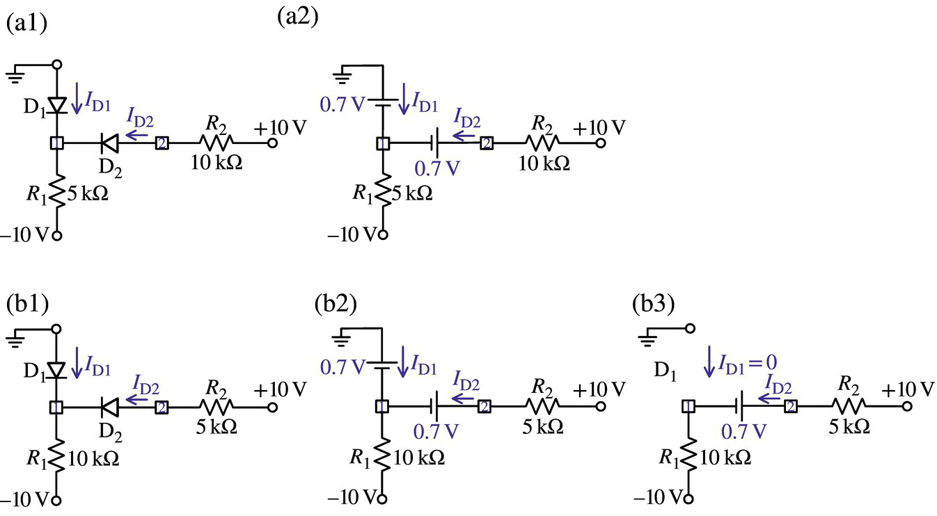
Figure P2.1.1 Diode circuits for Problem 2.1.
%elec02p01a.mclear, clfT=27; nVT=(T+273)/11605; % Temperature[Celsius] and Thermal voltageIs=1e-14; % Leakage current of the diodes% Diode exponential model parametersiD = @(vD)Is*(exp(vD/VT)-1); % Eq. (2.2.1a)R1=5e3; R2=10e3; % Circuit parameter valueseq = @(v)[iD(-v(?))+iD(v(2)-v(?))-(v(?)+10)/R1; ...iD(v(?)-v(1))-(10-v(?))/R2];v0 = [0; 0]; % Initial guess of [v1; v2]options=optimset('Display','off', 'TolX',1e-10, 'TolFun',1e-10);v = fsolve(eq,v0,options); % Solving the set of nonlinear eqsID1 = iD(-v(1)); ID2 = iD(v(?)-v(?));fprintf(' ID1=%8.3fmA, ID2=%8.3fmA, V1=%8.4fV, V2=%8.4fV\n', ID1*1e3,ID2*1e3,v(1),v(2));
- For a more exact analysis using the (nonlinear) exponential model (2.1.1) with Is = 1 × 10‐14[A] and VT = (27 + 273)/11605[V], apply Kirchhoff's current law (KCL) at nodes 1 and 2 to write two node equations as
- Consider the diode circuit of Figure P2.1.1(b1).
- First, assuming that both D1 and D2 are ON, replace them by the CVD model (with VD = 0.7 V) to draw the equivalent as shown in Figure P2.1.1(b2) and find the currents
 and
and  . If the solution turns out to be invalid, try with another assumption.
 - For a more exact analysis using the (nonlinear) exponential model (2.1.1) with IS = 6 × 10‐16 A, make a slight modification of the above MATLAB script “elec02p01a.m” and run it to find v1, v2,
 , and
, and  .
.
- First, assuming that both D1 and D2 are ON, replace them by the CVD model (with VD = 0.7 V) to draw the equivalent as shown in Figure P2.1.1(b2) and find the currents
- Perform the PSpice simulation of the diode circuit of Figure P2.1.1(a1) with the Analysis type of Bias Point by taking the following steps:
- Compose the PSpice schematic as shown in Figure P2.1.2(a).
- Create a simulation profile (with the analysis type of Bias Point) by selecting ‘Bias Point’ as the analysis type in the Simulation Settings dialog box as shown in Figure P2.1.2(b).
Run the PSpice schematic and click on the ‘Enable Bias Voltage Display’/‘Enable Bias Current Display’ button in the toolbar of the Capture CIS Window to see the bias‐point analysis results on voltages/currents at/through each node/branch.
- Consider the diode circuit of Figure P2.1.1(a1) where there are four possible states for the two diodes D1 and D2: ON-ON, ON-OFF, OFF-ON, and OFF-OFF.
- 2.2 Bridge Rectifier Circuit
Consider the bridge rectifier circuit of Figure P2.2(a) consisting of four diodes. Based on the (nonlinear) exponential model (2.1.1) with Is = 1 × 10⁻¹⁴[A] and VT = (27 + 273)/11605[V], apply KCL at nodes 1 and 2 to write two node equations as

Figure P2.1.2 PSpice simulation for the circuit of Figure P2.1.1(a1) – “elec02p01.opj.”

Figure P2.2 A bridge rectifier circuit and its analysis results for Problem 2.2.
(P2.2.1)
and use the MATLAB function ‘
fsolve()’ to solve them for v1 and v2 where vs(t) = 5 sin (2πt) [V]. To this end, complete the following MATLAB script “elec02p02.m” and run it to plot vs(t), vo(t) = v2(t), and − (the reverse
%elec02p02.mIs=1e-14; T=27; VT=(T+273)/11605; % Device parametersR=1e3; Vm=5; f=1; w=2*pi*f; % Circuit parameterst=[0:1e-3:2]; vs=Vm*sin(w*t); vst=[vs; t];[v1s,vos]=bridge_rectifier(vst,R,Is,VT);plot(t,vs, t,vos, t,vos-v1s,'m')function [v1s,v2s]=bridge_rectifier(vst,R,Is,VT)vs=vst(1,:); t=vst(2,:);iD=@(vD)Is*(exp(vD/VT)-1);options=optimoptions('fsolve','Display','none');for n=1:numel(t)vsn=vs(n);eq=@(v)[iD(v(1)-v(?))+iD(v(?)-vsn-v(2))-iD(-v(?))-iD(vsn-v(1));iD(v(?)-v(2))+iD(v(1)-vsn-v(?))-v(2)/R]*1e6;if n<2, v0=[0.7 0]; else v0=v; endv=fsolve(eq,v0,options);v1s(n)=v(1); v2s(n)=v(2);endvoltage of diode D2). Compare the waveforms with the PSpice simulation results shown in Figure 2.10c2.
- 2.3 Diode Clipping Circuits – Diode Limiters
%clippers.m% Copyleft: Won Y. Yang, wyyang53@hanmail.net, CAU for academic use onlyIs=10e-15; VT=25e-3; % Saturation current, Thermal voltageiDvD = @(vD)Is*(exp(vD/VT)-1).*(vD>0);iZvZ = @(vD,VZ0,rz)Is*(exp(vD/VT)-1).*(vD>0)-max (-VZ0-vD,0)/rz;vZiZ = @(iD,VZ0,rz,IZK)VT*???(iD/Is+1).*(iD>0) +... % Eq. (P2.3.1)(VZ0/???)*iD.*(-IZK<=iD&iD<0)-(iD<-IZK).*(VZ0-??*iD);options = optimset('TolFun',1e-10, 'Display','off');% Symmetrical diode limitervi=[-10:0.05:10]; % Range of the input signalRs=1e3; V1=2; V2=-2;vo=zeros(size(vi)); % Initialize the output voltage values to zerofor n=1:length(vi)eq = @(vo)(vi(n)-??)/Rs-iDvD(??-V1)+iDvD(V2-??);if n<2, vo0=0; else vo0=vo(n-1); endvo(n) = fsolve(eq,vo0,options);endsubplot(331), plot(vi,vo)% Symmetrical Zener limitervi=[-10:0.05:10]; % Range of the input signalVZ0=4.67; IZK=4e-12; VZ=4.7; IZ=2e-3; rz=(VZ-VZ0)/IZ % Eq. (2.3.1b)vo=zeros(size(vi)); % Initialize the output voltage values to zerofor n=1:length(vi)eq=@(i,VZ0,rz,IZK)vZiZ(?,VZ0,rz,IZK)-vZiZ(-?,VZ0, rz,IZK) +Rs*?-vi(n);...if n<2, i0=-1; else i0=i(n-1); endi(n) = fsolve(eq,i0,options,VZ0,rz,IZK); vo(n) = vi(n)-Rs*i(n);endsubplot(332), plot(vi,vo)% To plot the v-i characteristic curve of a Zener diodei=[-5:0.01:1]*1e-3; vz=vZiZ(i,VZ0,rz,IZK);subplot(333), plot(vz,i, [-5 1],[0 0],'k', [0 0], i([1 end]),'k')Consider the two diode clipping circuits (called limiters or clippers) each in Figure P2.3.1(a1) and (a2) where VT = 25 mV, the reverse saturation current of the diodes is Is = 10−14 A, and the Zener diode has VZ = 4.67/4.7 V at IZ = 0/2mA and IZK = 4 × 10⁻¹² A. Note that Figure P2.3.1(b1) and (b2) (obtained from PSpice simulation with Transient analysis) show their output voltage waveforms to sinusoidal input voltage of frequency 1 Hz and amplitude 5 V and 10 V, respectively, and Figure P2.3.1(c1) and c2 (obtained from PSpice simulation with DC sweep analysis and voltage source VSIN replaced by VDC) show their input-output relationships called voltage transfer characteristics (VTCs).

Figure P2.3.1 Diode clipping circuits (diode limiters) for Problem 2.3.
- Referring to Figure 2.19, complete the following equation describing the typical v-i characteristic of a Zener diode, which has been piecewise linear (PWL) approximated in the reverse‐biased region:
- Complete the sixth to seventh lines of the above MATLAB script “clippers.m” to create a MATLAB function handle defining the function vZ(iZ) with three parameters VZ0, rZ, and IZK where
(iZ>0),(‐IZK<=iZ&iZ<0), and(iZ<‐IZK)are logical expressions, each of which becomes 1 or 0 depending on whether it is true or not. Then noting that VZ0 = 4.67 V, use Eq. (2.3.1b) to determine the Zener resistance rZ and plot the v-i characteristic of the Zener diode, i.e. iZ versus vZ for iZ = (−5:0.01:1) × 10−3 [A] as shown in Figure P2.3.2(a) by running the last two lines of “clippers.m.” - To plot the v‐i characteristic (Figure P2.3.2(c)) of the Zener diode through PSpice simulation with DC sweep analysis, do the following:
- Create a PSpice schematic shown in Figure P2.3.2(b1) where the device parameters of the Zener diode part ‘DbreakZ’ are set in the PSpice Model Editor (opened by clicking on that part so that it will be highlighted in pink and selecting the menu Edit>PSpice Model) as shown in Figure P2.3.2(b2).

Figure P2.3.2 The v-i characteristic curve of the Zener diodes in Figure P2.3.1(a2).
- Click on New Simulation Profile button to open the Simulation Setting dialog box where you are supposed to set the Analysis type (DC Sweep), Sweep variable (Voltage source: Vi), and Sweep type (Linear: Start/End value = −4.8/0.8, Increment = 0.01) appropriately.
- Place a current marker at the anode of the Zener diode and run the PSpice schematic to see the VTC as shown in Figure P2.3.2(c).
- Create a PSpice schematic shown in Figure P2.3.2(b1) where the device parameters of the Zener diode part ‘DbreakZ’ are set in the PSpice Model Editor (opened by clicking on that part so that it will be highlighted in pink and selecting the menu Edit>PSpice Model) as shown in Figure P2.3.2(b2).
- Write the KCL equation in vo for node 1 in the clipper of Figure P2.3.1(a1) and the KVL equation in i for the mesh in the clipper of Figure P2.3.1(a2). With those equations, complete the above MATLAB script “clippers.m” so that it can plot the VTC curves of the two clippers. Run it to plot the VTCs and see if they are close to those shown in Figure P2.3.1(c1) and (c2).
- 2.4 Diode Clampers – DC Restorers
Consider the two diode clampers in Figure P2.4(a1) and (a2) that are driven by a PWL voltage source generating a square wave with magnitude ±5 V and period 2 s. Perform PSpice simulations of the clampers (with the SKIPBP box checked in the Simulation Settings dialog box) to get their input/output voltage waveforms as shown in Figure P2.4(b1) and (b2). Do their input-output relationships conform with Eqs. (2.2.1a) and (2.2.1b)?

Figure P2.4 Two clamper circuits and their PSpice simulation results (“dc:restorer.opj”).
- 2.5 MATLAB and PSpice Simulations of Voltage Doubler and Quadrupler
%voltage_doubler.mIs=2.682e-9; T=27; nVT=1.836*(273+T)/11605; % Diode constantsiDv=@(vD)Is*(exp(vD/nVT)-1);dt=0.001; tf=10; ts=0:dt:tf; Vm=5; f=2; w=2*pi*f; vs=Vm*sin(w*ts);C1=1e-6; C2=1e-6; vC1(1)=0; vC2(1)=0;for n=1:length(ts)vD1(n)=v?(n)-vC?(n); iD1(n)=iDv(vD1(n));vD2(n)=-vC?(n)-vD?(n); iD2(n)=iDv(vD2(n)); iC1(n)=iD?(n)-iD?(n);vC1(n+1) = vC1(n) + iC?(n)/C1*dt;vC2(n+1) = vC2(n) + sgn*iD?(n)/C2*dt;endplot(ts,vs,'r', ts,-vC2(1:end-1),'g'); grid on; legend ('vs(t)','vo(t)')Consider the voltage doubler/quadrupler circuits driven by a sinusoidal voltage source of amplitude 5 V and frequency 2 Hz, whose PSpice schematics are shown in Figures P2.5.1(a) and P2.5.2(a), respectively.
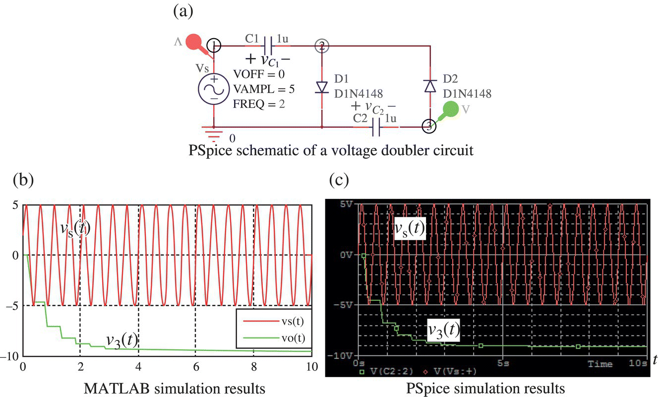
Figure P2.5.1 MATLAB and PSpice simulations of a voltage doubler circuit (“voltage_doubler.opj”).

Figure P2.5.2 PSpice and MATLAB simulations of a voltage quadrupler circuit (“voltage_quadrupler.opj”).
- Complete the above MATLAB script “voltage_doubler.m” to simulate the voltage doubler for 10s to get its input and output waveforms as shown in Figure P2.5.1(b). Also perform PSpice simulation of the circuit to get its input and output waveforms as shown in Figure P2.5.1(c).
- Complete the following MATLAB script “voltage_quadrupler.m” to simulate the voltage quadrupler for 10 s to get its input and output waveforms as shown in Figure P2.5.2(b). Also perform PSpice simulation of the circuit to get its input and output waveforms as shown in Figure P2.5.2(c).
%voltage_quadrupler.mclearIs=2.682e-9; T=27; nVT=1.836*(273+T)/11605; % Diode constantsiDv = @(vD)Is*(exp(vD/nVT)-1);dt=0.001; tf=10; ts=0:dt:tf; % Time vectorVm=5; f=2; w=2*pi*f; vs=Vm*sin(w*ts); % Input source voltageC1=1e-6; C2=1e-6; C3=1e-6; C4=1e-6;vC1(1)=0; vC2(1)=0; vC3(1)=0; vC4(1)=0;v2(1)=0; v3(1)=0; v4(1)=0; v5(1)=0;for n=1:length(ts)vD1 = v?(n); iD1 = iDv(vD1);vD2 = v?(n)-v?(n); iD2 = iDv(vD2);vD3 = v?(n)-v?(n); iD3 = iDv(vD3);vD4 = v?(n)-v?(n); iD4 = iDv(vD4);vC1(n+1) = vC1(n) + (iD1?iD2?iD3?iD4)/C1*dt;vC2(n+1) = vC2(n) + (iD2?iD3?iD4)/C2*dt;vC3(n+1) = vC3(n) + (iD3?iD4)/C3*dt;vC4(n+1) = vC4(n) + iD?/C4*dt;v2(n+1) = vs(n) - vC?(n+1);v3(n+1) = -vC?(n+1);v4(n+1) = v2(n+1) - vC?(n+1);v5(n+1) = v3(n+1) - vC?(n+1);endplot(ts,vs, ts,v5(1:end-1),'r'), grid on
- 2.6 Half‐wave Rectifier Circuit Fed by a Triangular Voltage Source Consider the half‐wave rectifier circuit of Figure P2.6(a) where the voltage source vi generates a triangular voltage waveform (with amplitude 10 V and frequency f = 1 kHz) shown in Figure P2.6(c).
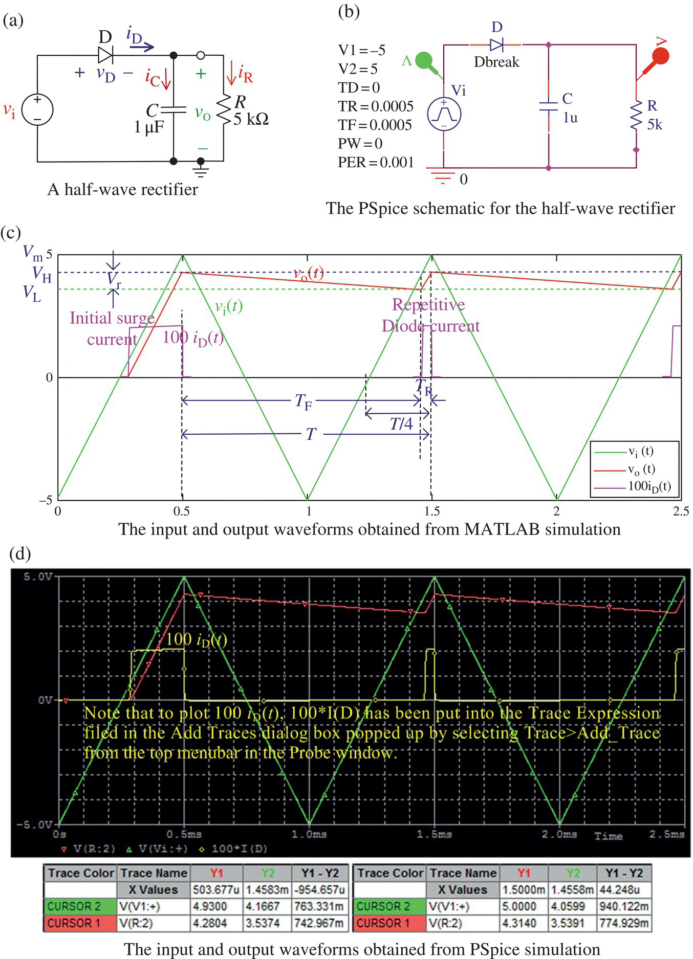
Figure P2.6 Half‐wave rectifier circuit fed by a triangular voltage source.
- To get the upper/lower limit VH/VL of the output voltage vo(t) and the rising/falling period TR/TF via an analytical approach using MATLAB, we set up the following equations like Eq. (2.2.3) referring to Figure P2.6(c):
(P2.6.1b)
 (P2.6.1c)
Noting that VH is already known as VH = Vm − VTD = 5 − 0.65 = 4.35, we can solve this set of equations to find VL = 3.94, TR = 0.02 ms, and TF = 0.98ms by saving these equations into an M‐file named, say, ‘elec02p06_f.m’ and running the following MATLAB script “elec02p06a.m.”
%elec02p06a.mglobal Vm f VTD T DVm=5; f=1000; T=1/f; D=T/2; VTD=0.65;VH=Vm-VTD; % Local maximum (High Voltage) of vo(t)R=5e3; C=1e-6;x_0=[0 0 0]; % Initial guess of [VL TR TF]x=fsolve('elec02p06_f',x_0,optimset('fsolve'),C,R)VL=x(1); TR=x(2); TF=x(3);fprintf('\n VH=%8.4f, VL=%8.4f, TR=%8.4fms, TF=%8.4fms',VH,VL,TR*1000,TF*1000)Vr=VH-VL, VH*T/R/C % Ripple Eq. (P2.6.2)IC_avg=C*Vr/TR; % Eq. (P2.6.4)Vo_avg=(VH?VL)/2 % Eq. (P2.6.5)IR_avg=Vo_avg/R % Eq. (P2.6.6)ID_avg=IC_avg?IR_avg % Eq. (P2.6.7)function y=elec02p06_f(x,C,R)global Vm f VTDVH=Vm-VTD; w=2*pi*f; T=1/f; VL=x(1); TR=x(2); TF=x(3);y=[VH*exp(-TF/R/C)-VL; VH-VL-4*Vm*TR/T; TR+TF-T]; % Eqs. (P2.6.1)
- To simulate the half‐wave rectifier by using MATLAB, complete and run the following script “elec02p06b.m” (after “elec02p06a.m”) to get the simulation result as shown in Figure P2.6(c).
%elec02p06b.mtf=2.5*T; dt=tf/5000; t=0:dt:tf; % Time range% Input voltagetri_wave_=@(t,D,T)mod(t,T)/D.*(mod(t,T)<D)+ ...(1-mod((t-D),T)/D).*(mod(t,T)>=D).*(mod(t,T)<2*D);vi = 2*Vm*tri_wave_(t,D,T)-Vm; % Input voltage waveform% RectificationIs = 1e-14; % Saturation current[vo,vD,iD,iR] = rectifier_RC([vi; t],R,?,Is);plot(t,vi,'g', t,vo,'r', t,100*iD,'m', t([1 end]),[0 0],'k')legend('v_i (t)','v_o (t)','100*i_D (t)')N1=floor(T/dt); nn0=1:N1;[VH,imin]=max(vo(nn0)); VH % Te 1st peak value of vo(t)tH1=t(imin); % The 1st peak timeN2=2*N1+10; nn1=N1:N2;[VL,imin]=min(abs(vo(nn1))); VLtL1=t(N1-1+imin); % The 1st valley time[emin,imin]=min(abs(vo(nn1)-VH));tH2=t(N1-1+imin); % The 2nd peak timeTF=tL1?tH1 % Falling periodTR=tH?-tL1 % Rising period - Assuming that TR ≪ T ≪ RC so that TF = T – TR ≈ T ≪ RC, show that the ripple voltage Vr = VH – VL is approximately
Noting that the capacitor voltage charged during the rising period TR is equal to the ripple voltage Vr and is related with the capacitor current iC or its average IC,avg is as
(P2.6.3)
find the average of the capacitor current through C:
Also, noting that the average of the output voltage (across R||C) is
find the average of the resistor current through R:
Also, find the average of the diode current through D:
- To simulate the half‐wave rectifier by using PSpice, draw the schematic as Figure P2.6(b) and perform the Transient analysis for 2.5 ms to get the input and output voltages and diode current as shown in Figure P2.6(d). You can activate or deactivate two cross cursors by clicking on the toggle cursor button in the PSpice A/D (Probe) window and move them to any two points by left‐/right‐clicking or pressing the (left or right) arrow/shift‐arrow to read their coordinates simultaneously where you can left‐/right‐click on the symbol of the variable (below the waveforms) which you want to read.
- Does the value of ID,avg agree with the (approximate) average of the diode current iD(t) (during the ON period) shown in Figure P2.6(c) or (d)?
- To get the upper/lower limit VH/VL of the output voltage vo(t) and the rising/falling period TR/TF via an analytical approach using MATLAB, we set up the following equations like Eq. (2.2.3) referring to Figure P2.6(c):
- 2.7 Precision Full‐wave Rectifier
Consider the precision full‐wave rectifier in Figure P2.7(a) where the maximum (saturation) output voltage and maximum (short‐circuit) output current of the OP Amp μA741 are Vom = 14.6 V and Ios = 40 mA, respectively, for a bipolar power supply of ±15 V.
- Noting that the OP Amp U1 has always a negative feedback path (via R2) so that v‐1 = v+1 by the virtual short principle, let us see how the rectifier works. If vi > 0, vo0 becomes (low, high) so that D1 can be (off, on) and thus io0 = 0,
 = 0, and v−1 = v+1 = vi. Then
  so that
  . If vi < 0, vo0 becomes (low, high) so that D1 can be (off, on) to activate the negative feedback path for the OP Amp U2, resulting in
  (virtual ground). Then the OP Amp U1 functions as an inverting amplifier with gain −R2/R1 so that
  .
. - Doesn't the value of R3 seem to matter? To check your idea, resimulate the rectifier with R3 = 100 Ω to get vo(t), v‐2(t), and 10iD(t) as shown in Figure P2.7(c) where vo(t) has been severely distorted in the middle of the negative cycle of vi(t). Why is that? It is because v−1 = v+1 = v−2 ≠ v+2 = 0, i.e. the virtual short principle does not hold despite the negative feedback path via D1 with iD = io0 > 0. What caused this situation starting from just when vi is about to decrease below −4 V so that −
 = io0 is going to increase over (v+1 − vi)/R3 = (v−2 − vi)/R3 = 40 mA = Ios? What is the minimum value of R3 to avoid such a situation?

Figure P2.7 A precision full‐wave rectifier.
- Noting that the OP Amp U1 has always a negative feedback path (via R2) so that v‐1 = v+1 by the virtual short principle, let us see how the rectifier works. If vi > 0, vo0 becomes (low, high) so that D1 can be (off, on) and thus io0 = 0,
- 2.8 Precision Full‐wave Rectifier
Consider the precision full‐wave rectifier with the PSpice schematic shown in Figure P2.8(a) where R1 = R2 = R3 = R4 = R5 = 1 kΩ and the maximum (saturation) output voltage of the OP Amp μA741 is Vom = 14.6 V for a bipolar power supply of ±15 V.
- Noting that the OP Amp U1 as well as U2 has always a negative feedback path via R2-D1 (when vi > 0) or via D2-R5 (when vi < 0) so that v‐1 = v+1 = 0 and v‐2 = v+2 by the virtual short principle, let us see how the rectifier works. When vi > 0, vo0 becomes (low, high) so that D1/D2 can be (on/off, off/on) and thus
 ,
,  where both U1 and U2 work as linear amplifiers each with gain −R2/R1 and
 –R4/R3, respectively. Then(P2.8.1)
When vi < 0, vo0 becomes (low, high) so that D1/D2 can be (on/off, off/on). KCL at node 1 yields a node equation with v3 as an unknown variable:
(P2.8.2)

Figure P2.8 A precision full‐wave rectifier.
Then, regarding R2-R3-R4 as a voltage divider, we can find the output voltage vo as
(P2.8.3)
- Find the peak inverse voltages (PIVs) of the diodes D1 and D2.
When vi = Vm = 5 V, vo0 becomes low so that D1 is on with
 =
=  = 0.7 V and D2 is reverse‐biased with
When vi = −Vm = −5 V, vo0 becomes high so that D2 is on with
 =
=  = 0.7 V and D1 is reverse‐biased with(P2.8.4)
These PIVs can also be seen from the simulation result in Figure P2.8(b).
- Noting that the OP Amp U1 as well as U2 has always a negative feedback path via R2-D1 (when vi > 0) or via D2-R5 (when vi < 0) so that v‐1 = v+1 = 0 and v‐2 = v+2 by the virtual short principle, let us see how the rectifier works. When vi > 0, vo0 becomes (low, high) so that D1/D2 can be (on/off, off/on) and thus
- 2.9 Zener (Shunt) Regulator
Consider the Zener regulator shown in Figure 2.20(a) where the Zener diode has VZ = 6.8 V at IZ = 5 mA, rZ = 20 Ω, and IZK = 0.2 mA, and the supply voltage vS varies by ±1 V around its nominal value 10 V.
- Determine VZ0 of the linear iZ‐vZ relation (2.3.1b) describing the almost‐straight line part of the i‐v characteristic curve of the Zener diode.
Substituting (IZ, VZ) = (5 mA, 6.8 V) and rz = 20 Ω into Eq. (2.3.1b) yields
(P2.9.1)
- Use the equivalent circuit (Figure 2.20(b)) with the Zener diode Z replaced by its PWL model to find the output voltage vo = vZ (across RL = 2 kΩ in parallel with the Zener diode) to the source voltage vs = 10, 9, 8.3 V.
We can use Eq. (2.3.8) to get
>>([10 9 8.3]/500+6.7/20)/(1/500+1/20+1/2000)However, for the third value vZ = 6.697 V < VZ0, we set iZ = 0 (IZK) and use the voltage divider rule to redetermine vZ as if there were no Zener diode branch:
(P2.9.3)
- Make use of Eq. (2.3.9a) to guess how vZ (the voltage across the Zener diode or RL = 2 kΩ) will be changed by the ±1V‐change in vs.
(P2.9.4)

You can run the following MATLAB statements to get a help in finding the answers to the above questions:
>>VZ=6.8; IZ=5e-3; rz=20; IZK=0.2e-3;vss=[10 9 8.3]; Rs=500; RL=2e3;[vos,iZ,dvodvs,dvodRL,dvodIL,Rsmax,RLmin,VZ0]= ...Zener_regulator(VZ,IZ,rz,IZK,RL,Rs,vss)Is your guess close to the real change in vZ (across RL = 2 kΩ to vs = 10V) caused by the −1V‐change in vs, which can be observed in Eq. (P2.9.2)?
- Use the equivalent circuit (Figure 2.20(b)) to find the output voltage vo = vZ (across RL = 2, 1.9, 1.4 kΩ in parallel with the Zener diode) to the source voltage vs = 9 V.
We can use Eq. (2.3.8) to get
>>(9/500+6.7/20)./(1/500+1/20+1./[2 1.9 1.4]/1e3)However, for the third value vZ = 6.696 V < VZ0, we set iZ = 0 (IZK) and use the voltage divider rule to redetermine vZ as if there were no Zener diode branch:
(P2.9.6)
- Make use of Eq. (2.3.9b) to guess how vZ (to vs = 9 V) will be changed by the ±100 Ω‐change in RL.
(P2.9.7)

You can run the following MATLAB statements to get a help in finding the answers to the above questions:
>>vs=9; Rs=500; RLs=[2e3 1.9e3 1.4e3];[vos,iZ,dvodvs,dvodRL,dvodIL,Rsmax,RLmin,VZ0]=...Zener_regulator(VZ,IZ,rz,IZK,RLs,Rs,vs); vos, dvodRLIs your guess close to the real change in vZ (across RL = 2 kΩ to vs = 9V) caused by the −100 Ω‐change in RL, which can be observed in Eq. (P2.9.5)?
- To see that for vs ≤ 8.3V, vZ gets distinctly away from VZ = 6.8V at RL = 2 kΩ, perform a PSpice simulation by taking the following steps:
- Draw the PSpice schematic including a DC voltage source Vdc (10V), a sinusoidal voltage source VSIN (with amplitude 2 V and frequency 1 Hz), a Zener diode DbreakZ, two resistors Rs = 500 Ω and RL = 2 kΩ, and a Ground, as shown in Figure P2.9.1(a). If DbreakZ is not found in the Part List (Part Browser dialog box) when you type ‘DbreakZ’ in the Part text box of the Place Part dialog box (Figure P2.9.1(b)) opened by Place part button on the tool palette (Figure P2.9.1(a)), you should insert the BEAKOUT library into the Libraries list by clicking on the Add library button and selecting Cadence > … > tools > capture > library > pspice > breakout.olb.

Figure P2.9.1 PSpice simulation for the Zener regulator in Problem 2.9 (“voltage_regulator_zener0.opj”).
- Select the symbol of DbreakZ by clicking on it, select ‘Edit > PSpice Model’ (from the menu bar) to open the PSpice Model Editor window, and type ‘BV = 6.8V IBV = 5mA’ to set VZ = 6.8V and IZ = 5 mA (Figure P2.9.1(c)).
- Set the Analysis type, Run to time, and Maximum step size as ‘Time Domain (Transient)’, 2 s, and 1 ms, respectively, in the Simulation Settings dialog box opened by clicking on the New/Edit Simulation Profile button from the toolbar (Figure P2.9.1(d)).
- Place the voltage markers at the upper terminals of the voltage source Vs and resistor RL as shown in Figure P2.9.1(a).
- Click Run to start the simulation and get the input/output voltage waveforms as shown in Figure P2.9.2.

Figure P2.9.2 PSpice simulation results for Problem 2.9.
Does the output voltage vZ drop conspicuously below VZ = 6.8V as the source voltage vs becomes lower than 8.3V? How can the value of vZ to the input source voltage vs = 8V be estimated?
- Draw the PSpice schematic including a DC voltage source Vdc (10V), a sinusoidal voltage source VSIN (with amplitude 2 V and frequency 1 Hz), a Zener diode DbreakZ, two resistors Rs = 500 Ω and RL = 2 kΩ, and a Ground, as shown in Figure P2.9.1(a). If DbreakZ is not found in the Part List (Part Browser dialog box) when you type ‘DbreakZ’ in the Part text box of the Place Part dialog box (Figure P2.9.1(b)) opened by Place part button on the tool palette (Figure P2.9.1(a)), you should insert the BEAKOUT library into the Libraries list by clicking on the Add library button and selecting Cadence > … > tools > capture > library > pspice > breakout.olb.
- Determine VZ0 of the linear iZ‐vZ relation (2.3.1b) describing the almost‐straight line part of the i‐v characteristic curve of the Zener diode.


