© Springer Nature Switzerland AG 2020
K. Y. ChengIII–V Compound Semiconductors and DevicesGraduate Texts in Physicshttps://doi.org/10.1007/978-3-030-51903-2_2

2. Atomic Bonding and Crystal Structures

Keh Yung Cheng1, 2  
(1)
Department of Electrical and Computer Engineering, University of Illinois at Urbana-Champaign, Urbana, Illinois, USA
(2)
Department of Electrical Engineering, National Tsing Hua University, Hsinchu, Taiwan
 
 
Keh Yung Cheng

Abstract

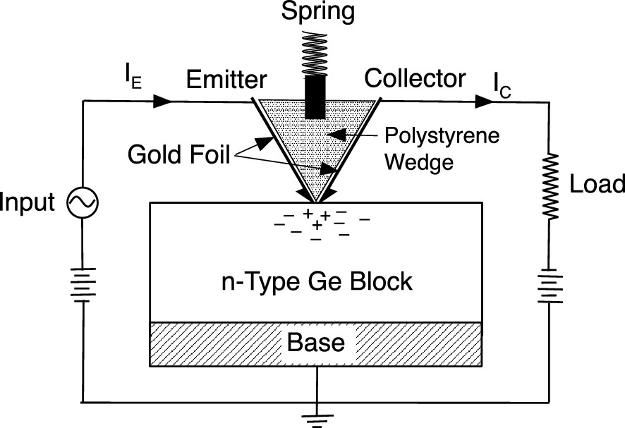
On December 23, 1947, John Bardeen and Walter Brattain demonstrated the world’s first transistor at Bell Telephone Laboratories. The point-contact transistor was made in the area of a large single-crystalline grain on a piece of reused polycrystalline germanium. Above the Ge slab was a polystyrene wedge structure where, at the bottom tip of the wedge, the gold-foil emitter and collector electrodes make point contacts, separated by ~50 µm, to the n-type Ge base. In this device, the injection of both electrons and holes into a semiconductor was first demonstrated. Shortly after that, the zone refining process was developed by William Pfann for the growth of silicon and germanium crystals of predetermined purity. Today, transistors, light-emitting diodes, injection lasers, integrated circuits, and many other semiconductor devices are made from single crystals of semiconductor material with extremely high purity. There are other semiconductor devices which are not made from single-crystal material, though they could be and their operation is usually obtained as if they were. Hence, a study of the basic properties of crystal structures is necessary for a meaningful explanation of the operation of semiconductor devices. In this chapter, the tetrahedron bond structure—the basic building block of major semiconductor crystals—is first derived from atomic sp3 orbitals. The reciprocal lattice is then introduced as an alternative but powerful approach to investigate the lattice structure of the crystal. For example, crystal diffraction results are best discussed in the reciprocal lattice space. Finally, the Brillouin zone concept is introduced.

2.1 Crystal Structures and Symmetry
../images/325043_1_En_2_Chapter/325043_1_En_2_Fig1_HTML.png
Fig. 2.1

Schematic of the point-contact bipolar transistor invented by Bardeen and Brattain of Bell Telephone Laboratories in 1947. The polystyrene wedge covered with gold foil on two sides was held against the Ge with a spring to form emitter and collector contacts. The n-type Ge slab forms the base of the transistor. Minority carrier (hole) injection was demonstrated for the first time

2.1.1 Crystal Structures
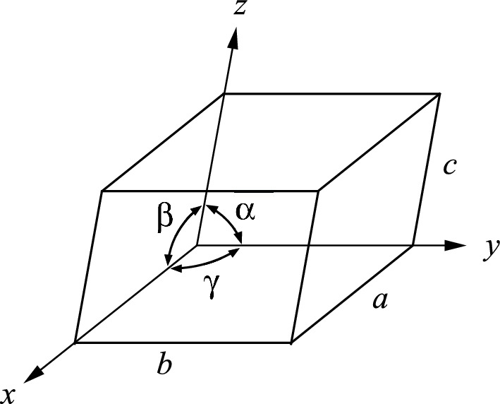
The solids of primary interest for us are semiconductors that have all their atoms arranged in a regular pattern in three dimensions (3D). Such solids are called single crystals, and the arrangement of atoms is termed the crystal structure. The basic 3D building blocks that pack together to fill all the space of the crystal are called the unit cells. A unit cell can be seen as a parallelepiped defined by three lengths a, b, and c and three angles α, β, and γ as shown in Fig. 2.2. By changing the lengths and angles of the parallelepiped, while making sure to fill all the space, a number of crystal structures can be built. Depending on the specifications about the lengths and the angles, these crystal structures are classified into seven systems as listed in Table 2.1. Some structures can be derived from other crystal structures. For example, under a uniaxial stress, such as in a strained quantum well, a cubic crystal can be transformed into an orthorhombic structure. Additionally, these basic structures are further modified by four different 3D unit cells: (a) The primitive unit cell (symbol P) has a lattice point at each corner and forms a minimum volume. (b) The body-centered unit cell (symbol I) has a lattice point at each corner and one at the center of the cell. (c) The face-centered unit cell (symbol F) has a lattice point at each corner and one at the center of each face. (d) The base-centered unit cell (symbol A, B, or C) has a lattice point at each corner and one pair of opposite faces; e.g., a C-centered cell has lattice points in the centers of the ab faces. When combing these four types of lattice with seven possible unit cell forms, 14 Bravais lattices are produced. For example, the simple cubic is the primitive unit cell of the cubic system while the body-centered cubic and face-centered cubic correspond to the modified (I and F, respectively) cubic unit cells (Fig. 2.3). It is important to note that the lattice point represents equivalent positions in a crystal structure and not atoms. A lattice point could be occupied either by an atom, a complex ion, a single molecule, or a group of molecules.
../images/325043_1_En_2_Chapter/325043_1_En_2_Fig2_HTML.png
Fig. 2.2

Definition of axes, dimensions and angles for a general unit cell

Table 2.1

Seven crystal classes and related Bravais lattices

System

Unit cell

Bravais lattice

Cubic

a = b = c, α = β = γ = 90°

P (primitive), I (body-centered), F (face-centered)

Hexagonal

a = b ≠ c, α = β = 90°, γ = 120°

P (rhombohedral)

Tetragonal

a = b ≠ c, α = β = γ = 90°

P, I

Orthorhombic

a ≠ b ≠ c, α = β = γ = 90°

P, I, F, C (base-centered)

Monoclinic

a ≠ b ≠ c, α = β = 90° ≠ γ

P, C

Trigonal

a = b = c, 120° > α = β = γ ≠ 90°

P (rhombohedral)

Triclinic

a ≠ b ≠ c, α ≠ β ≠ γ

P

../images/325043_1_En_2_Chapter/325043_1_En_2_Fig3_HTML.png
Fig. 2.3

Four basic 3D Bravais lattices most relevant to semiconductor crystals. The face-centered cubic and hexagonal crystal structures are particularly important in semiconductor physics

2.1.2 Crystallographic Notation—Miller Indices
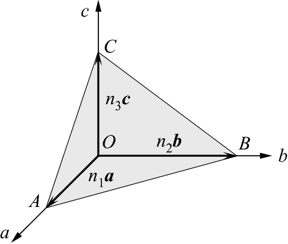
In semiconductor technologies, we often make devices and circuits on a particular crystallographic plane or a particular direction of semiconductor crystals. This particular crystal plane is usually described by its Miller indices, which are established as follows. Consider a 3D lattice, a portion of which is shown in Fig. 2.4, where A, B, C, and O are lattice points; a, b, and c are translational unit vectors; and n1, n2, and n3 are the proper integers. Thus the plane ABC can be defined by vectors OA (=n1a), OB (=n2b), and OC (=n3c). For reasons that will become clear when the properties of reciprocal lattices are explored in Sect. 2.5, we shall find it useful to refer to the ABC plane as the (hkl) plane, where hkl is a set of integers which expresses the ratio
../images/325043_1_En_2_Chapter/325043_1_En_2_Fig4_HTML.png
Fig. 2.4

Description of the construction of Miller indices for the plane passing through the lattice points A, B, and C. a, b, and c are unit vectors and n1, n2, and n3 are integers

$$ h :\,k :\,l = \frac{1}{{n_{1} }} :\,\frac{1}{{n_{2} }} :\,\frac{1}{{n_{3} }} $$
(2.1)
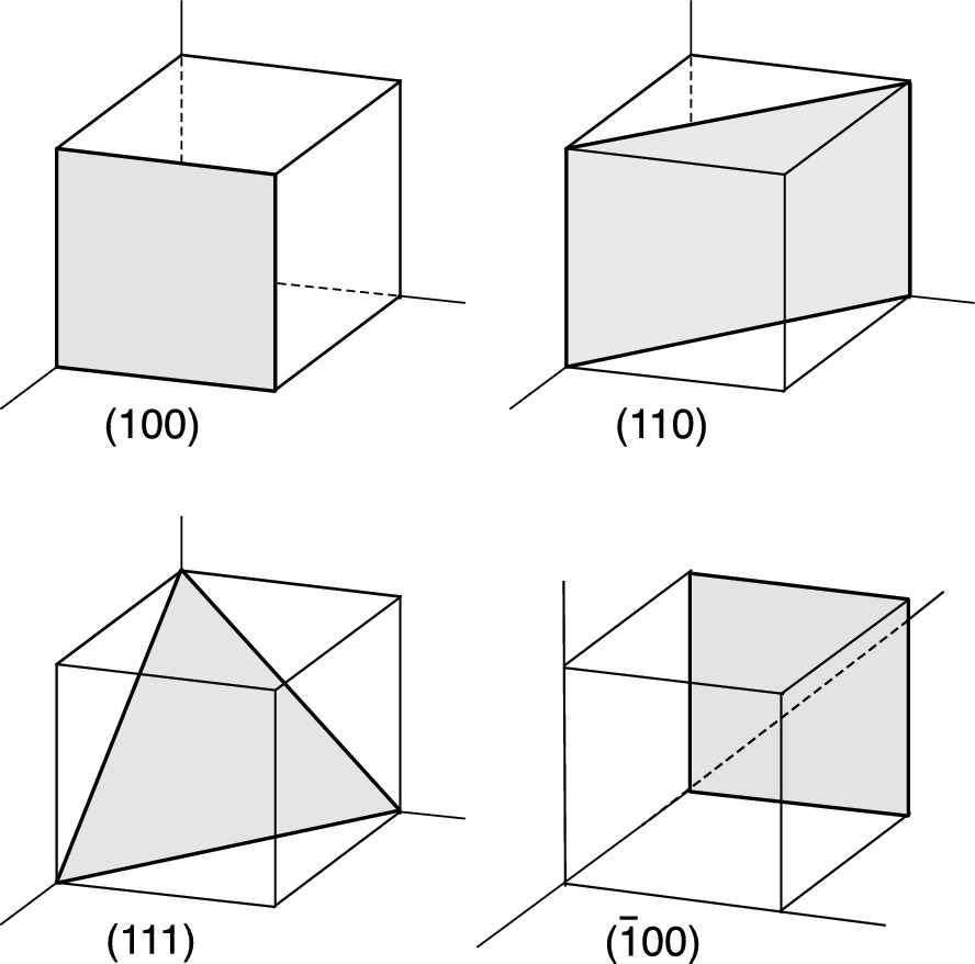
Thus the plane ABC has the Miller indices of (hkl) which are a set of the smallest integers that satisfy (2.1). For example, for the plane whose intercepts are 2, 1, 3, the reciprocals are $$ \raise.5ex\hbox{$\scriptstyle 1$}\kern-.1em/ \kern-.15em\lower.25ex\hbox{$\scriptstyle 2$} $$, 1, and $$ {\raise0.5ex\hbox{$\scriptstyle 1$}\kern-.1em/ \kern-.15em\lower.25ex\hbox{$\scriptstyle 3$}} $$; the smallest three integers having the same ratio are (362). If a plane cuts an axis (say, the a-axis) on the negative side of the origin, the corresponding index is negative, indicated by placing a bar (minus sign) above the index as ($$ \bar{h}kl $$). For an intercept at infinity, the corresponding index is zero. Figure 2.5 illustrates the Miller indices of some important plans in a cubic crystal. The indices (h00) may denote a plane parallel to both b- and c-axes, e.g., the (100) plane, and the indices (hk0) represent a plane parallel to the c-axis. The normal to the plane with indices (hkl) is the direction [hkl]. In a cubic crystal there are six cubic faces: (100), (010), (001), ($$ \bar{1}10 $$), ($$ 0\bar{1}0 $$), and ($$ 00\bar{1} $$). This set of equivalent planes of a cubic crystal may be denoted as a group by {100}. The family of plane directions in the cubic crystal may be expressed as 〈100〉.
../images/325043_1_En_2_Chapter/325043_1_En_2_Fig5_HTML.png
Fig. 2.5

Miller indices of some important planes in a cubic crystal

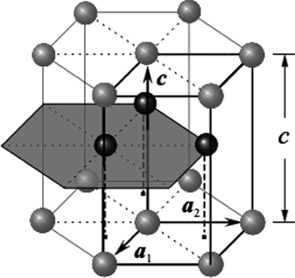
For hexagonal crystal structures, there are four coordinates, namely the a1, a2, a3, and c axes as shown in Fig. 2.6. The angle between adjacent ai’s is 120°. Therefore, it is common to use a set of four Miller indices, expressed in terms of the reciprocal intercepts with respect to the vectors a1, a2, a3, and c as (hkjl). However, it can be proved that the sum of h, k, and j of a plane is always zero. Thus the added index j serves as a check and does not provide any new information. For example, the shaded surface shown in Fig. 2.6 cuts a1 and a2 at 1 and −1, respectively, and is parallel to a3 and c. Thus this plane may be designated as $$ \left( {1\bar{1}00} \right) $$ according to
../images/325043_1_En_2_Chapter/325043_1_En_2_Fig6_HTML.png
Fig. 2.6

Four unit vectors used to formulate Miller indices for a hexagonal crystal

$$ h{:}\,k{:}\,j{:}\,l = \frac{1}{1}:\frac{1}{ - 1}:\frac{1}{\infty }:\frac{1}{\infty } = 1: - 1:0:0 $$
where h + k + j = 1 − 1 + 0 = 0. The Miller indices of the base of the hexagonal crystal, or the basal plane, are (0001).

2.1.3 Lattice Symmetries

As discussed earlier, a single-crystal solid has all its atoms arranged in a regular pattern in three dimensions. The unit cells or building blocks of the crystal are shaped as 14 basic parallelepipeds of Bravais lattices. Any two locations in the crystal having identical atomic environment can be achieved through a simple translation action on the unit cells following
$$ \varvec{T} = n_{1} \varvec{a} + n_{2} \varvec{b} + n_{3} \varvec{c} $$
(2.2)
where T is the translation vector; a, b, and c are the unit vectors; and n1, n2, and n3 are integers. In addition, lattice points can be recurred into themselves by other operations including (a) reflection at a plane, (b) inversion through a point, (c) rotation about an axis, and (d) rotation-inversion about an axis.
Using simple cubic structure as an example, these operations are illustrated in Fig. 2.7. Through the operation of reflection at a mirror plane, the xy plane in Fig. 2.7a, point P may transform to point Q. This symmetry is expressed mathematically by a coordinate transformation x′ = x, y′ = y, and z′ = –z. The tensor representation of the mirror reflection operation in the xy plane is expressed as
../images/325043_1_En_2_Chapter/325043_1_En_2_Fig7_HTML.png
Fig. 2.7

Symmetry operations in a cubic crystal. a Reflection at a plane, b inversion through a point, c rotation about an axis, and d rotation-reflection about an axis

$$ \left[ {\begin{array}{*{20}c} 1 & 0 & 0 \\ 0 & 1 & 0 \\ 0 & 0 & { - 1} \\ \end{array} } \right]\left[ {\begin{array}{*{20}c} x \\ y \\ z \\ \end{array} } \right] = \left[ {\begin{array}{*{20}c} x \\ y \\ { - z} \\ \end{array} } \right] $$
(2.3)

The presence of a mirror plane in a crystal is represented by the symbol m. The inversion symmetry operation (Fig. 2.7b) may be described by the coordinate transformation x′ = –x, y′ = –y, and z′ = –z. It may also be expressed by the transformation of the position vector r′ = –r at the inversion point. The symbol of the inversion symmetry is $$ \bar{I} $$. The other symmetry operation is the rotation about an axis. The axis of rotation is named an n-fold axis if the angle ϕ of rotation to carry a unit cell into itself is equal to ϕ = 2π/n. In this example, Fig. 2.7c, a 90° rotation about the axis will bring point P to point Q or a fourfold symmetry. All possible rotation operations are one-, two-, three-, four-, and sixfold symmetry, which correspond to rotations by 2π, π, 2π/3, π/2, and π/3 radians. These are the only five allowed rotation symmetry operations since they are consistent with a crystal’s requirements for translational symmetry.

The symmetry operations may be combined with one another in various ways. For example, there is a rotation-reflection compound operation to carry the lattice into itself. As shown in Fig. 2.7d, a 90° (fourfold) rotation about an axis parallel to the z-axis through the center of the cube combining with a mirror reflection at the xy plane will bring points P and Q to S and R, respectively. This combined operation is represented by the symbol $$ \bar{n} $$ for the n-fold rotation symmetry. Conversely, every crystal may be described by a particular combination of symmetry elements that strongly influence its material properties. More specifically, this combination determines the nature of independent components of the tensors describing macroscopic material properties.

To illustrate this correlation, we examine the dielectric constant $$ \epsilon $$ of the material using the symmetry concept and tensor representation. By definition, $$ \varvec{D} = \epsilon \varvec{E} $$ or
$$ \left[ {\begin{array}{*{20}c} {D_{x} } \\ {D_{y} } \\ {D_{z} } \\ \end{array} } \right] = \left[ {\begin{array}{*{20}c} {\epsilon_{11} } & {\epsilon_{12} } & {\epsilon_{13} } \\ {\epsilon_{21} } & {\epsilon_{22} } & {\epsilon_{23} } \\ {\epsilon_{31} } & {\epsilon_{32} } & {\epsilon_{33} } \\ \end{array} } \right]\left[ {\begin{array}{*{20}c} {E_{x} } \\ {E_{y} } \\ {E_{z} } \\ \end{array} } \right] $$
(2.4)
For a cubic crystal, there are four threefold (along diagonals as shown in Fig. 2.8) and three fourfold (along three major axes) rotation axes. When rotating along [111] for 120°, it brings, for example, x → y, y → z and z → x. In tensor form, it is
../images/325043_1_En_2_Chapter/325043_1_En_2_Fig8_HTML.png
Fig. 2.8

Rotation symmetry operations along a [111] and b $$ [\bar{1}11] $$ axes of a cubic crystal

$$ \left[ {\begin{array}{*{20}c} {D_{y} } \\ {D_{z} } \\ {D_{x} } \\ \end{array} } \right] = \left[ {\begin{array}{*{20}c} {\epsilon_{11} } & {\epsilon_{12} } & {\epsilon_{13} } \\ {\epsilon_{21} } & {\epsilon_{22} } & {\epsilon_{23} } \\ {\epsilon_{31} } & {\epsilon_{32} } & {\epsilon_{33} } \\ \end{array} } \right]\left[ {\begin{array}{*{20}c} {E_{y} } \\ {E_{z} } \\ {E_{x} } \\ \end{array} } \right] $$
(2.5)
Equations (2.4) and (2.5) are essentially the same and their components can be compared. By examining Di in both equations, we can deduce the relations of some tensor components
$$ D_{x} = \epsilon_{11} E_{x} + \epsilon_{12} E_{y} + \epsilon_{13} E_{z} = \epsilon_{31} E_{y} + \epsilon_{32} E_{z} + \epsilon_{33} E_{x} $$
(2.6a)
and
$$ D_{y} = \epsilon_{21} E_{x} + \epsilon_{22} E_{y} + \epsilon_{23} E_{z} = \epsilon_{11} E_{y} + \epsilon_{12} E_{z} + \epsilon_{13} E_{x} $$
(2.6b)
By comparison, we have $$ \epsilon_{11} = \epsilon_{22} = \epsilon_{33} ,\epsilon_{13} = \epsilon_{21} = \epsilon_{32} , $$ and $$ \epsilon_{12} = \epsilon_{31} = \epsilon_{23} $$. The threefold rotation symmetry exists along the other rotation axes. A rotation of 120° about $$ [\bar{1}11] $$ will bring x →y, y → z, z →x (Fig. 2.8b), or
$$ \left[ {\begin{array}{*{20}c} { - D_{y} } \\ {D_{z} } \\ { - D_{x} } \\ \end{array} } \right] = \left[ {\begin{array}{*{20}c} {\epsilon_{11} } & {\epsilon_{12} } & {\epsilon_{13} } \\ {\epsilon_{21} } & {\epsilon_{22} } & {\epsilon_{23} } \\ {\epsilon_{31} } & {\epsilon_{32} } & {\epsilon_{33} } \\ \end{array} } \right]\left[ {\begin{array}{*{20}c} { - E_{y} } \\ {E_{z} } \\ { - E_{x} } \\ \end{array} } \right] $$
(2.7)
Comparing (2.4), (2.5), and (2.7), we find $$ \epsilon_{12} = - \epsilon_{23} = \epsilon_{31} $$ and $$ \epsilon_{13} = \epsilon_{21} = - \epsilon_{32} $$. In order to fulfill both these results obtained from the two different rotation axes, we conclude that $$ \epsilon_{ij} = 0 $$ for ij and $$ \epsilon_{11} = \epsilon_{22} = \epsilon_{33} $$. Thus,
$$ \epsilon = \left[ {\begin{array}{*{20}c} {\epsilon_{11} } & 0 & 0 \\ 0 & {\epsilon_{11} } & 0 \\ 0 & 0 & {\epsilon_{11} } \\ \end{array} } \right] $$
(2.8)

Therefore, the simple cubic crystal has an isotropic dielectric constant $$ \epsilon $$.

Using a similar approach, we can calculate the dielectric constant tensors in other crystals. For hexagonal crystals, the dielectric constant tensor has the form
$$ \epsilon = \left| {\begin{array}{*{20}c} {\epsilon_{11} } & 0 & 0 \\ 0 & {\epsilon_{11} } & 0 \\ 0 & 0 & {\epsilon_{33} } \\ \end{array} } \right| $$
(2.9)
if the z-axis is chosen to be the axis of sixfold symmetry and the x- and y-axes are the two perpendicular axes in the basal plane. Thus, the symmetry considerations help us find the relations that may exist between the matrix elements in a material parameter tensor such as the dielectric constant tensor. Therefore, we can expect the less symmetric zinc-blende crystal structure of GaAs to have an anisotropic dielectric constant and nonlinear optical properties.

2.2 Ionic Bond and Inter-atomic Forces

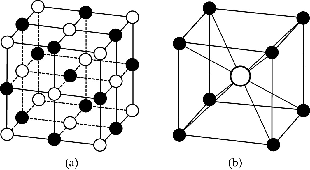
Ionic crystals are generally transparent insulators of inorganic compounds. The crystal structures of some ionic crystals are simple, such as NaCl and CsCl, while others are extremely complex. For the purpose of studying the properties of ionic bonding, we consider the simple compound NaCl. Sodium (Na), an alkali metal, has a single 3s valence electron outside the closed shell, whereas chlorine (Cl), a halogen, is one electron short of having a complete outer 3p shell. As shown in Fig. 2.9, an electron transfer from the alkali metal to the halogen results in closed-shell configurations in both Na+ and Cl ions. During this electron transfer process, there are four major energy exchanges involved in forming the ionic bond. First, the energy given up when a neutral (Cl) atom gains an electron and becomes a negative ion (anion) is called the electron affinity. It increases the energy of the system and has a positive value. Second, the energy necessary to remove an electron from the (Na) atom creating a positive ion (cation) is simply the ionization energy—a negative energy value. Third, the Coulomb force between Na+ and Cl ions keeps these ions together in a Na+Cl ionic crystal, and a lowering of potential energy occurs. Therefore, the Coulomb attraction force has a positive energy value. Finally, when the electron shells of the neighboring ion cores start to overlap, a repulsive force must be considered. The repulsive energy is a result of the Pauli exclusion principle for a closed ion shell. Energy is required to prevent the collapse of the lattice and is considered a negative term. The balance of competing requirements for attractive and repulsive components of the electrostatic interaction warrants that highly symmetric crystal structures ensue with maximized volumes. Figure 2.10 shows two of the simplest ionic crystal structures of all—the rock salt structure of NaCl and the cesium chloride (CsCl) structure. The NaCl structure can be viewed as an FCC crystal with a basis containing one Na+ ion at (0, 0, 0) and one Cl ion at ($$ \raise.5ex\hbox{$\scriptstyle 1$}\kern-.1em/ \kern-.15em\lower.25ex\hbox{$\scriptstyle 2$} ,\raise.5ex\hbox{$\scriptstyle 1$}\kern-.1em/ \kern-.15em\lower.25ex\hbox{$\scriptstyle 2$} ,\raise.5ex\hbox{$\scriptstyle 1$}\kern-.1em/ \kern-.15em\lower.25ex\hbox{$\scriptstyle 2$} $$). The other way of constructing the NaCl structure is to position alternatively with Na+ or Cl ions at the lattice sites of a simple cubic crystal. Each ion is surrounded by six nearest-neighbor ions of the opposite type in 〈100〉 directions. The CsCl structure is based on the simple cubic crystal structure with a basis containing one Cs+ ion at (0,0,0) and one Cl ion at ($$ \raise.5ex\hbox{$\scriptstyle 1$}\kern-.1em/ \kern-.15em\lower.25ex\hbox{$\scriptstyle 2$} ,\raise.5ex\hbox{$\scriptstyle 1$}\kern-.1em/ \kern-.15em\lower.25ex\hbox{$\scriptstyle 2$} ,\raise.5ex\hbox{$\scriptstyle 1$}\kern-.1em/ \kern-.15em\lower.25ex\hbox{$\scriptstyle 2$} $$). The structure looks like BCC but, strictly speaking, is not since different ions occupy the two lattice sites at the body center and corners. There are eight nearest-neighbor ions of the opposite type in 〈111〉 directions.
../images/325043_1_En_2_Chapter/325043_1_En_2_Fig9_HTML.png
Fig. 2.9

Electron configuration in NaCl. The outer ring represents the shell of n = 3. The dashed arrow indicates the electron transfer from Na to Cl resulting in closed shell configurations in Na and Cl ions. The Coulomb attraction between two ions and repulsive force between cores are also shown
../images/325043_1_En_2_Chapter/325043_1_En_2_Fig10_HTML.png
Fig. 2.10

Two typical ionic crystal structures: a NaCl and b CsCl. The ionic radii of Na+, Cs+, and Cl are 0.875 Å, 1.455 Å, and 1.475 Å, respectively
../images/325043_1_En_2_Chapter/325043_1_En_2_Fig11_HTML.png
Fig. 2.11

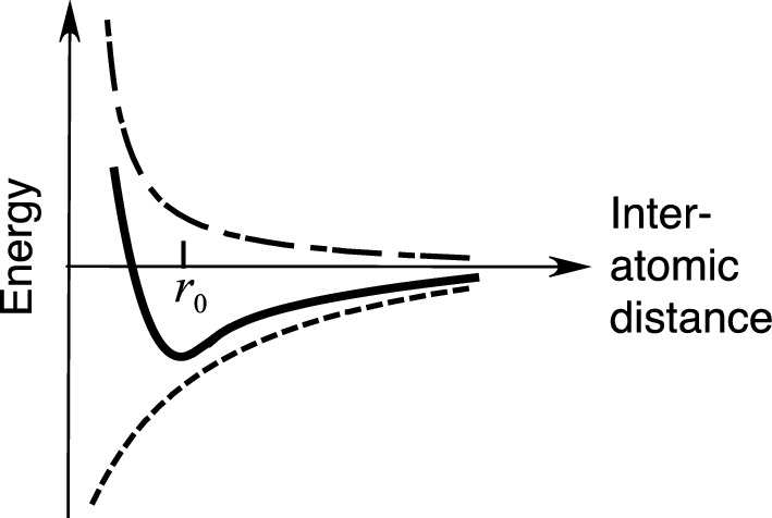
Total potential energy as a function of the separation of two ions. The dot-dashed and dashed curves correspond to contributions of repulsive and Coulomb attraction forces, respectively. r0 is the equilibrium separation of ions

The total energy required to separate the atoms in the solid into isolated neutral atoms and vice versa is called the cohesive energy or binding energy, E0. Since the ionization energy of the positive ion and the electron affinity of the negative ion very nearly cancel each other, the major contribution to the binding energy is the electrostatic energies. We can formulate these relations in the following equation:
$$ E_{\text{T}} \left( r \right) \cong E_{\text{Coul}} \left( r \right) + E_{\text{Rep}} \left( r \right) $$
(2.10)
where ET is the sum of the Coulomb attraction energy ECoul and the energy of the repulsive force ERep at a positive ion–negative ion separation distance r. In a NaCl crystal structure, surrounding any Na+ are six neighboring Cl ions, 12 next-nearest-neighboring Na+ ions, and so forth. The Coulomb energy can be calculated as
$$ \begin{aligned} E_{\text{Coul}} & = - \frac{{q^{2} }}{{4\pi \epsilon_{0} r}}\left( {\frac{6}{1} - \frac{12}{\sqrt 2 } + \frac{8}{\sqrt 3 } - \frac{6}{\sqrt 4 } + \frac{24}{\sqrt 5 } - \cdots } \right) = - 1.748\frac{{q^{2} }}{{4\pi \epsilon_{0} r}} = \\ & \quad - \alpha \frac{{q^{2} }}{{4\pi \epsilon_{0} r}} \\ \end{aligned} $$
(2.11)
where α is the Madelung constant which has the values of 1.641, 1.638, and 1.763 for wurtzite, zinc-blende, and CsCl structures, respectively. The negative sign of ECoul represents the net attractive force between ions. Since the repulsive force decreases rapidly as the distance between ions increases, it has a power-law form of
$$ E_{\text{Rep}} = \frac{A}{{r^{n} }} \propto r^{ - n} $$
(2.12)
where A and n are constants and ERep has a positive value. Thus the sum of (2.11) and (2.12) gives the total energy.
$$ E_{\text{T}} \left( r \right) = - \frac{{\alpha q^{2} }}{{4\pi \epsilon_{0} r}} + \frac{A}{{r^{n} }} $$
(2.13)
A qualitative expression of ET(r) is plotted in Fig. 2.11. At equilibrium, r = r0,
$$ \frac{{{\text{d}}E_{\text{T}} }}{{{\text{d}}r}} = \frac{{\alpha q^{2} }}{{4\pi \epsilon_{0} r_{0}^{2} }} - \frac{nA}{{r_{0}^{n + 1} }} = 0 $$
where r0 is the equilibrium inter-atomic distance of the ionic crystal. Thus,
$$ r_{0}^{n - 1} = \frac{{4\pi \epsilon_{0} nA}}{{\alpha q^{2} }} $$
(2.14)
The cohesive or binding energy E0 is obtained from the total energy ET(r) at r = r0.
$$ E_{0} = E_{\text{T}} \left( {r_{0} } \right) = \left( {E_{\text{Coul}} + E_{\text{Rep}} } \right)_{{r_{0} }} = - \frac{{\alpha q^{2} }}{{4\pi \epsilon_{0} r_{0} }}\left( {1 - \frac{1}{n}} \right) $$
(2.15)

For stability of the crystal, n must be greater than unity. Of course it should be possible to determine it from an exact quantum mechanical treatment of the problem. However, from a fit to experimental quantities, n has been determined to be in the range 6–10. Therefore, the Coulomb attraction force becomes the major contributor to the cohesive energy.
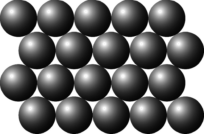
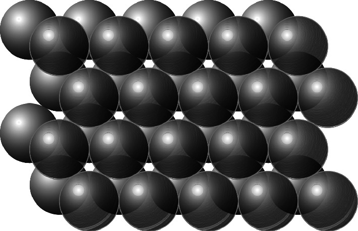
In general, the ionic bond is a non-directional bond. It forms a close atomic packing to maximize the number of bonds per unit volume and to minimize the bonding energy per unit volume. Due to the size difference between ions, it can form either a simple cubic or FCC structure to avoid anion–anion or cation–cation contact. The condition that determines the crystal structure can be understood by using a ‘hard sphere’ model. Imagine the atoms as small hard spheres. When identical atoms are assembled in a layer, the most compact arrangement is the close-packed structure in which every sphere has six touching neighbors. This plane array, as shown in Fig. 2.12, has a hexagonal symmetry and is assigned as layer A. To build up a close-packed solid in 3D we must now add a second layer, B. The spheres of the second layer will sit in half of the holes of the first layer as shown in Fig. 2.13. When we come to add the third layer, C, there are two possible positions where it can fit. First, it could be positioned on top of layer B so that its atoms sit in the holes of layer B which were also holes in layer A. A fourth layer identical to layer A can then be added and the ABCABC sequence continued. This is known as cubic close packing and produces a FCC lattice. The stacking layer surfaces simply correspond to the {111} surface of the FCC structure. An alternative form of close packing is to position the third layer C identically to layer A, to fit on top of layer B. When we repeat this sequence, the pattern of ABABAB produces a hexagonal close-packed (HCP) structure. For cations and anions of similar size, the simple cubic structure (CsCl) is preferred to achieve the highest packing density. Otherwise, it will form an FCC structure (NaCl). Due to their large cohesive energies, these alkali halides, which are among the most stable ionic crystals, have large bandgaps. For example, the bandgaps for NaCl and CsCl are 8.5 and 8.4 eV, respectively.
../images/325043_1_En_2_Chapter/325043_1_En_2_Fig12_HTML.png
Fig. 2.12

Hard spheres arranged in a close-packed layer structure
../images/325043_1_En_2_Chapter/325043_1_En_2_Fig13_HTML.png
Fig. 2.13

Two layers of close-packed spheres

2.3 Covalent Bond and sp3 Hybrid Orbit

2.3.1 General Properties of Covalent Bond Formation

Atoms in molecule or solid can ‘share’ their electrons to form a covalent bond. The simplest example is the N2 molecule. The nitrogen atom has an electron configuration of 1s22s22p3. The 2p shell needs six valence electrons to fill its outermost orbit. This can be accomplished by sharing six electrons (three from each atom) between two nitrogen atoms (Fig. 2.14). These shared electrons orbit the two nitrogen atoms, spending equal time with each. Therefore they do not specifically belong to a particular nitrogen atom, but are shared by both. These shared electrons ‘bond’ two nitrogen atoms into a nitrogen molecule. We shall discuss the physics of the bond formation in detail next.
../images/325043_1_En_2_Chapter/325043_1_En_2_Fig14_HTML.png
Fig. 2.14

Schematic of the formation of covalent bonding in a nitrogen molecule. The circles in each nitrogen atom represent the unfilled 2p valence electron states

To illustrate the relation of electron distribution behavior and bonding formation, we use the H2+ ion as an example, in which the two protons are held together by one electron. For an isolated hydrogen atom, the wave function has a spherical symmetric form of
$$ \psi \left( {1s} \right) = \frac{1}{{\sqrt {\pi a_{0}^{3} } }}\exp \left( { - r/a_{0} } \right) $$
(2.16)
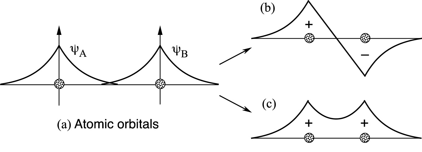
where a0 is the Bohr radius. The wave functions of two nearby but independent hydrogen atoms, as described by (2.16), are shown in Fig. 2.15a. As the protons are brought closer together to form the H2+ ion, the interaction between the electron and two protons leads to two possible wave functions as derived by quantum mechanical calculation. The two lowest energy states have either symmetric (even) wave function or anti-symmetric (odd) wave function. The change in sign for the anti-symmetric wave merely means that the two wave functions associated with ions are 180° out of phase. From these wave functions, the corresponding probability densities of the electron distribution can be easily estimated as shown in Fig. 2.16. For the anti-symmetric wave function, there is no electron near the center of the system. In the case of symmetric wave function, there is a high probability of an electron existing in the middle of the two nuclei. Different electron distributions directly relate to the energy profile of the system. The potential energy of the system is given as
../images/325043_1_En_2_Chapter/325043_1_En_2_Fig15_HTML.png
Fig. 2.15

Formation of bonding and anti-bonding combinations of atomic orbitals in diatomic hydrogen molecules with a single bonding electron. a The wave functions of two nearby hydrogen atoms. b The anti-symmetric wave function and c symmetric wave function formed in a H2+ ion

../images/325043_1_En_2_Chapter/325043_1_En_2_Fig16_HTML.png
Fig. 2.16

Probability density of the electron distribution in a H2+ ion with a anti-symmetric and b symmetric wave functions

$$ E_{\text{PE}} = - E_{e - n} + E_{n - n} $$
(2.17)
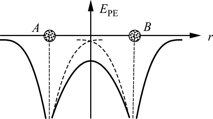
where −Een represents the electron–nucleus attraction energy and Enn represents the nucleus–nucleus repulsion energy (Fig. 2.16b). The high probability of finding electrons in between two nuclei increases the attractive force contribution (more negative) to EPE. As shown in Fig. 2.17, this decreases the potential energy distribution near the center and forms the primary mechanism for the covalent bonding (bonding state). In the anti-symmetry case, the lack of electrons in between two cores means it is unfavorable to form a covalent bond (anti-bonding state).
../images/325043_1_En_2_Chapter/325043_1_En_2_Fig17_HTML.png
Fig. 2.17

Potential energy of the H2+ ion (solid curves). The dashed curve is the potential energy of a single hydrogen nucleus

In other words, the spatial overlap of the wave functions ψA and ψB leads to the splitting of the original energy level Es, associated with the ψ(1s) state, into a higher and a lower molecular energy level (Fig. 2.18). The molecular orbital corresponding to the higher energy level is the anti-bonding state. The bonding state is where the electron occupies the lower-lying bonding orbital, thereby giving rise to a reduction in the total energy. This energy reduction corresponds to the binding energy of the covalent bond.
../images/325043_1_En_2_Chapter/325043_1_En_2_Fig18_HTML.png
Fig. 2.18

Energy level diagram shows the relative position of bonding (Eb) and anti-bonding (Ea) energies with respect to isolated ψ(1s) state energy (Es). The related wave functions are also shown

Now, let us turn our attention to hydrogen molecules where there are two valence electrons. When forming covalent bonding in H2 molecules, the two valence electrons are shared equally by the two nuclei. The symmetric electron wave functions from the two electrons have the same quantum numbers n, l, and m. They, then, must have opposite spin orientations (s = ± 1/2) or anti-parallel spins to comply with the Pauli exclusion principle. Thus, in a covalent bond the two shared electrons must have anti-parallel spins, and this is also known as the electron-pair bond. This concept applies to other materials, such as N2, which has been discussed earlier. The six 2p electrons in a N2 molecule are bound in pairs with spins aligned anti-parallel in each pair as shown Fig. 2.19a.
../images/325043_1_En_2_Chapter/325043_1_En_2_Fig19_HTML.png
Fig. 2.19

Electron-pair bond formed in between a pair of electrons in p orbital with anti-parallel spin in a N2, b PH3, and c H2O. The dotted arrows indicate hydrogen electrons which make pair-bonds with p electrons of phosphorous and oxygen

We further examine this idea in water (H2O) and phosphine (PH3) (Fig. 2.19). The oxygen has an electron configuration 1s22s22p4, and phosphorous has an electron configuration 1s22s22p63s23p3. Since the s electrons in the outer shell already have their spins paired, only the p electrons need to be considered. For a phosphorous atom, there are three electrons that have unpaired spins, whereas for an oxygen atom, two of the four electrons already have paired spins leaving two electrons having unpaired spins. Therefore, a phosphorous atom is capable of making three electron-pair bonds with three hydrogen atoms in PH3, and an oxygen atom is capable of forming two electron-pair bonds in H2O.

2.3.2 Directional Property of Covalent Bonds

In forming covalent bonds, the accumulated electrons in between the nuclei result in the overlapping of wave functions. A strong bond is formed if there is a maximum wave function overlap. The orbital wave functions of an atom can be derived using a simple model of a hydrogen atom consisting of a proton and a single electron that interact through electrostatic attraction. The wave function in 3D space is expressed as $$ \psi (r,\theta ,\phi ) = R(r){\varTheta (}\theta {)\varPhi (}\phi \text{)} $$ where R, Θ, and Φ are the radial, azimuthal, and angular wave functions, respectively. The algebraic expressions for some of the wave functions are given below.
$$1s^{2} {:}\;\psi_{100} = N_{100} \exp \left( { - \frac{r}{{a_{0} }}} \right) $$
(2.18a)
$$ 2s^{2} {:}\; \psi_{200} = N_{200} \left( {2 - \frac{r}{{a_{0} }}} \right)e\left( { - \frac{r}{{2a_{0} }}} \right) $$
(2.18b)
$$ 2p^{6} {:}\; \left\{ {\begin{array}{*{20}l} {\psi_{210} = N_{210} \left( {\frac{r}{{a_{0} }}} \right)\exp \left( { - \frac{r}{{2a_{0} }}} \right)\cos \theta                    } \\ {\psi_{211} = N_{211} \left( {\frac{r}{{a_{0} }}} \right)\exp \left( { - \frac{r}{{2a_{0} }}} \right)\sin \theta \exp \left( {i\phi } \right)    } \\ {\psi_{{21\bar{1}}} = N_{{21\bar{1}}} \left( {\frac{r}{{a_{0} }}} \right)\exp \left( { - \frac{r}{{2a_{0} }}} \right)\sin \theta \exp \left( { - i\phi } \right)} \\ \end{array} } \right. . $$
(2.18c)
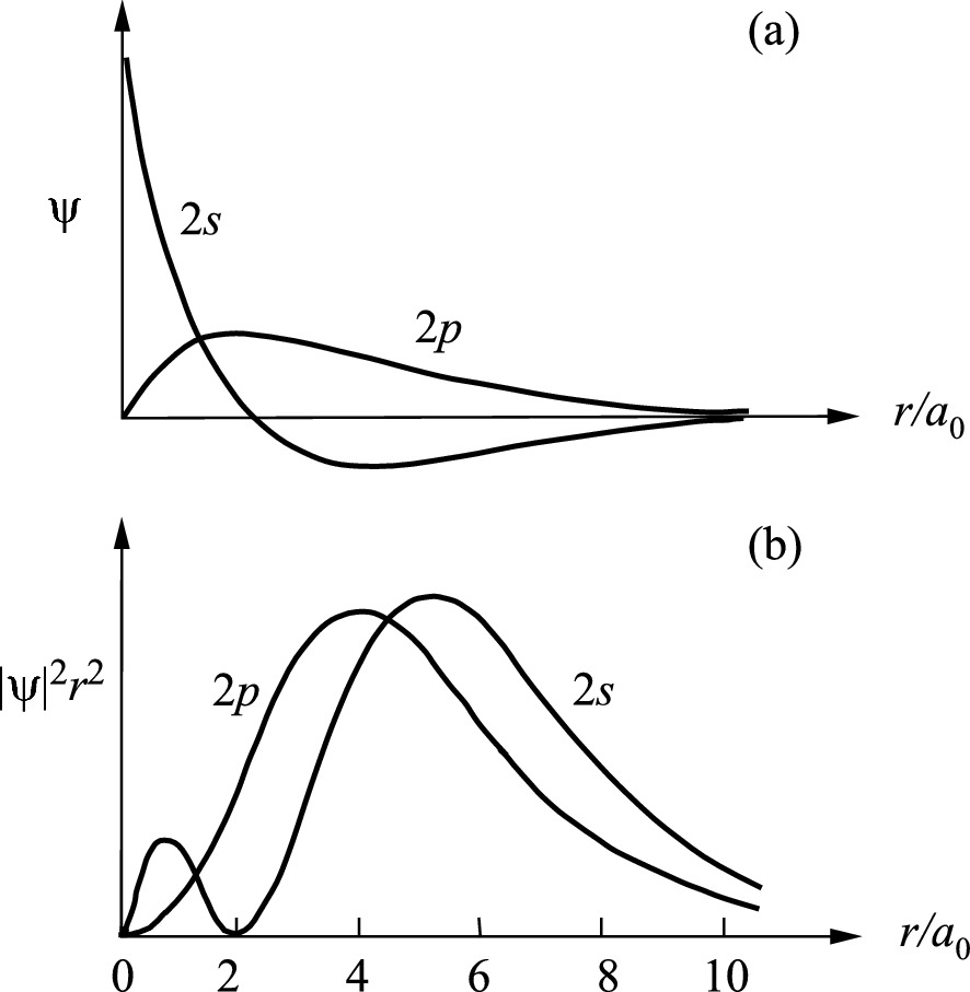
where a0 is the Bohr radius. The superscripts to s and p above indicate the allowed degeneracy of the state. The radial wave functions for the 2s state (ψ200) and 2p state (ψ210) are shown in Fig. 2.20a. The probability density distributions of the s states are always spherically symmetric, while the p, d, f states, etc., have angular dependence. For example,
../images/325043_1_En_2_Chapter/325043_1_En_2_Fig20_HTML.png
Fig. 2.20

a Radial wave functions Rnl(r) and b radial probability density |ψ|2r2 of the 2s (ψ200) and 2p (ψ210) states of the hydrogen atom as a function of radial distance r in the unit of Bohr radius a0

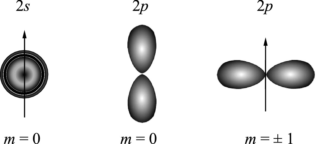
$$ \left\{ {\begin{array}{*{20}c} {\left| {\psi_{210} } \right|^{2} \propto r^{2} \exp \left( { - \frac{r}{{a_{0} }}} \right)\cos^{2} \theta } \\ {\left| {\psi_{21 \pm 1} } \right|^{2} \propto r^{2} \exp \left( { - \frac{r}{{a_{0} }}} \right)\sin^{2} \theta } \\ \end{array} } \right. $$
(2.19)
Figure 2.21 shows the shape of the probability density distributions for 2s and 2p states in space for a hydrogen atom. However, it is not |ψ|2 itself but the integration of |ψ|2 over the volume that represents the correct electron distribution in a 3D system. In a spherical system like the hydrogen atom model, the volume increases rapidly with the radius r and the larger values of r should be weighted heavily. Therefore, it is more interesting to find the probability that the electron is between r and (r + dr),
../images/325043_1_En_2_Chapter/325043_1_En_2_Fig21_HTML.png
Fig. 2.21

Electron density distributions of 2s and 2p states for a hydrogen atom. The polar (z) axis is oriented vertically

$$ \left| \psi \right|^{2} {\text{d}}\upsilon = \left| \psi \right|^{2} r^{2} \sin \theta {\text{d}}r{\text{d}}\phi {\text{d}}\theta = \left| \psi \right|^{2} 4\pi r^{2} {\text{d}}r \propto \left| \psi \right|^{2} r^{2} . $$
(2.20)

Figure 2.20 shows the electron wave functions and the corresponding radial probability densities (|ψ|2r2) of 2s and 2p states in a hydrogen atom. Note that the radial probability density distributions of s and p states overlap heavily. More 2s electrons than 2p electrons are occupying states at larger r. As we will see in the next section, these results have important consequences in determining crystal structures of semiconductors. Consider the case of mixing s and p orbital wave functions. The s orbits (l = 0) of an atom always have a spherical symmetry, i.e., ψs = g(r). For p orbits (l = 1), the wave functions are angularly dependent as described in (2.18c). Consequently, the spatial distribution of the wave functions leads to a strong orientation dependency in covalent bonding.

Let us take a closer look at the spatial overlap between s and p wave functions. Since the linear combination of ψ210 and ψ21±1 is also a solution to the Schrödinger wave equation, we can transform the polar components of wave functions to the Cartesian coordinates with
$$ \left\{ {\begin{array}{*{20}l} {x = r\,\sin \,\theta \cos \,\phi } \hfill \\ {y = r\,\sin \,\theta \sin \,\phi } \hfill \\ {z = r\,\cos \,\theta         } \hfill \\ \end{array} } \right. $$
(2.21)
Thus,
$$ \left\{ {\begin{array}{*{20}l} {\psi_{211} + \psi_{{21\bar{1}}} \propto x} \hfill \\ {\psi_{211} - \psi_{{21\bar{1}}} \propto y} \hfill \\ {\psi_{210} \propto z             } \hfill \\ \end{array} } \right. $$
(2.22)
Letting R(r) = rf(r), we can express the three p wave functions as
$$ \psi_{px} = xf\left( r \right),\psi_{py} = yf\left( r \right),\,{\text{and}}\,\psi_{pz} = zf\left( r \right) $$
(2.23)
The shapes of ψs and ψp’s are shown in Fig. 2.22. Each p orbital extends along a specific coordinate axis, e.g., the x-axis for the ψpx orbital. Therefore, when ψs and ψp overlap to form a covalent bond, only certain ψp orientations will provide a maximum overlap of electron distributions with ψs. The covalent bond will be formed along one of these orientations to achieve a bond of maximum strength.
../images/325043_1_En_2_Chapter/325043_1_En_2_Fig22_HTML.png
Fig. 2.22

Spherical s orbital and three p orbitals each directed along a different Cartesian axis

2.3.3 sp3 Hybrid Orbit

In semiconductor crystals, the atomic bonds are not structured in the form of pure s or p wave function but a mixture of them. We will use the electron configuration of the methane (CH4) molecule to illustrate the hybrid orbitals. For a carbon atom, the electron configuration is shown in Fig. 2.23a (1s22s22p2). The inner s orbitals are all full. For the 2p orbital, there are only two unpaired electrons available for four single valence electrons from hydrogen atoms to form electron-pair bonds. A closer examination reveals that the energy levels of 2s and 2p states are very close to each other, and, as shown in Fig. 2.20b, the probability density |ψ(2p)|2r2 overlaps heavily with |ψ(2s)|2r2. Therefore, one of the two electrons in the 2s state can be elevated to the empty 2p state. Promoting one of the two electrons to the empty 2p state increases the energy of the system. But this allows four electrons from hydrogen atoms to form more electron-pair bonds, which decreases the total energy of the system. Thus, the electron configuration of a carbon atom is changed into 1s22s12p3 in a methane molecule. This new configuration has a maximum of four unpaired electrons and is ready to form CH4 molecules by bonding with electrons from four hydrogen atoms. The electron configuration of the methane molecule now looks like that shown in Fig. 2.23b.
../images/325043_1_En_2_Chapter/325043_1_En_2_Fig23_HTML.png
Fig. 2.23

Electron-pair bond formed in a carbon atom, and b CH4. The dotted boundary indicates the bonding orbitals. The dotted arrows are sites available for electron-pair bonds

The 2s1p3 configuration in methane is called sp3 hybridization. If an s-orbital is mixed with three p-orbitals, four sp3-hybrids are generated. The wave functions of the four sp3 hybrid orbitals in a CH4 molecule can be derived by linear combinations of s and p state (2.23) wave functions.
$$ \left\{ {\begin{array}{*{20}c} {\psi_{111} = \frac{1}{2}\left[ {\psi_{s} + \psi_{x} + \psi_{y} + \psi_{z} } \right]} \\ {\psi_{{1\bar{1}\bar{1}}} = \frac{1}{2}\left[ {\psi_{s} + \psi_{x} - \psi_{y} - \psi_{z} } \right]} \\ {\psi_{{\bar{1}1\bar{1}}} = \frac{1}{2}\left[ {\psi_{s} - \psi_{x} + \psi_{y} - \psi_{z} } \right]} \\ {\psi_{{\bar{1}\bar{1}1}} = \frac{1}{2}\left[ {\psi_{s} - \psi_{x} - \psi_{y} + \psi_{z} } \right]} \\ \end{array} } \right. $$
(2.24)
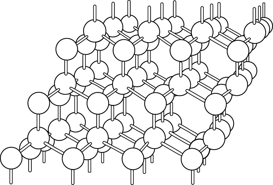
Four sp3 orbitals are identical in shape, each one having a large lobe and a minor lobe as shown in Fig. 2.24a. The four orbitals are oriented in the space such that the large lobes form a tetrahedral arrangement. These new hybrid orbitals on carbon are used to share electron pairs with the 1s orbitals from the four hydrogen atoms to form a methane molecule, as shown in Fig. 2.24b. Once the methane molecule is formed, there is no extra unpaired free bond to link with other methane molecules. Therefore, a CH4 crystal can only be formed by van der Waals bonding force. The bonding structure of CH4 is a tetrahedron structure that is determined by optimizing repulsive forces between hydrogen atoms. The tetrahedron bond structure represents the basic form of all semiconductor crystals. For example, the silicon atom has an electron configuration of 1s22s22p63s23p2. The four unpaired electrons in the 3s and 3p states form sp3 hybrid orbits for crystal bonding. Each Si atom is bonded with four neighboring Si atoms in a tetrahedron structure shown in Fig. 2.25a. This basic tetrahedron structure can propagate indefinitely in all directions as illustrated in Fig. 2.26. As will be discussed in more detail in Sect. 2.4, the resultant crystal has a diamond structure. For GaAs, the Ga (1s22s22p63s23p63d104s24p1) and As (1s22s22p63s23p63d104s24p3) can also bind in the diamond-like (zinc-blende) structure with tetrahedron coordination (Fig. 2.25b). Each Ga atom is surrounded by four As atoms and vice versa. The shared bonding electrons consist of five electrons from the As atom and three electrons from the Ga. The total number of electrons per atom is the same as in the case of the diamond structure of carbon or silicon.
../images/325043_1_En_2_Chapter/325043_1_En_2_Fig24_HTML.png
Fig. 2.24

a A set of four sp3 orbitals forms a tetrahedron with each sp3 orbital containing a large lobe and a small lobe. The large lobes point to the corners of the tetrahedron and can be used to share electrons in covalent bonds. b The sp3 hybrid orbitals of carbon in a CH4 molecule, each having an electron distribution directed toward one of the four alternating corners of a cube

../images/325043_1_En_2_Chapter/325043_1_En_2_Fig25_HTML.png
Fig. 2.25

Tetrahedron bond structure of a Si and b GaAs
../images/325043_1_En_2_Chapter/325043_1_En_2_Fig26_HTML.png
Fig. 2.26

An infinite tetrahedron arrangement of a covalent bonded diamond cubic structure.

Reprinted with permission from [1], copyright Oxford University Press

2.3.4 Mixed Ionic-Covalent Bonds

In pure covalent crystals like Si and diamond, the binding orbital between the nearest neighbors is a linear combination of hybridized orbitals from each atom and the wave function of the binding orbital can be expressed as
$$ \psi_{b} \sim \psi_{ 1} + \psi_{ 2} $$
(2.25)
where ψ1 and ψ2 are the wave functions of the two nearest-neighbor atoms. Due to symmetry, the electrons shared in a bond must spend, on the average, ‘equal time’ on each atom. This leads to a symmetrical distribution of the electron density and to a purely covalent bond.
In compound semiconductors, the bonding orbitals are less ideal than the pure covalent bond and the sharing of bonds is not so obvious. Consider GaAs as an example, where there are three and five valence electrons associated with Ga (4s24p1) and As (4s24p3) atoms, respectively. On average, there are four bonds per Ga atom sharing with four As atoms. In the simplest picture, each group V atom donates an electron to a group III atom so that each atom has four valence electrons with sp3 hybrid orbitals. This situation can be expressed as
$$ {\text{Ga}}\left( {4s^{2} 4p^{1} } \right) + {\text{As}}\left( {4s^{2} 4p^{3} } \right) \to {\text{Ga}}\left( {4s^{1} 4p^{3} } \right)^{ - } + {\text{As}}\left( {4s^{1} 4p^{3} } \right)^{ + } $$
(2.26)
However, this also leads to the formation of III and V+ ions. The situation can be seen partially as electron sharing and partially as electron transfer. Shared electrons in the bonding states spend a greater fraction of time on the cation, similar to a partially ionic bond. Thus, the time-averaged wave function for a bonding electron is
$$ \psi_{b} \sim \psi_{\text{cov}} + \lambda \psi_{\text{ion}} $$
(2.27)
where ψcov and ψion are wave functions for completely covalent and ionic forms, respectively. The weighting factor λ, called the ionicity parameter, determines the degree of ionicity (fi):
$$ f_{i} = \frac{{\lambda^{2} - 1}}{{\lambda^{2} + 1}} $$
(2.28)
Another measure of ionicity in a compound is the difference in the electronegativity of its constituent elements as suggested by Linus Pauling. The electronegativity of an element represents the power of an atom to attract an electron to itself in a compound. Therefore, the electronegativity difference is well correlated with the ionicity of a compound. For purely covalent crystals such as Si and Ge, fi = 0. For III–V compound semiconductors, the theoretical ionicity values along with their crystal structures are listed in Table 2.2. It is interesting to note that compounds with large ionicity value (fi ≥ 0.45), e.g., III-nitride compounds, tend to crystallize in wurtzite structure rather than zinc-blende crystal structure.
Table 2.2

Crystal structure and ionicity for III–V compound semiconductors. (W = wurtzite structure; ZB = zinc-blende structure) [2]

III–V

Structure

Ionicity

III–V

Structure

Ionicity

III–V

Structure

Ionicity

AlN

W

0.449

GaN

W

0.500

InN

W

0.578

AlP

ZB

0.307

GaP

ZB

0.374

InP

ZB

0.421

AlAs

ZB

0.274

GaAs

ZB

0.310

InAs

ZB

0.357

AlSb

ZB

0.426

GaSb

ZB

0.261

InSb

ZB

0.321

2.4 Major Semiconductor Crystal Structures

2.4.1 Diamond Structure

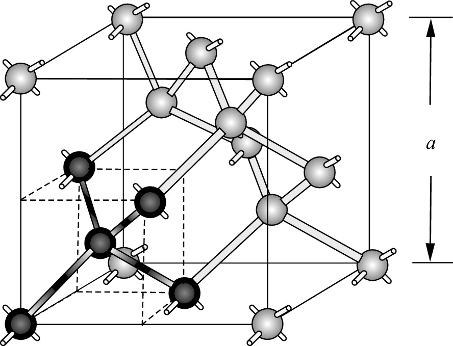
To generate a large silicon crystal, we must always fit silicon atoms together in the four-nearest-neighbor pattern suggested in Fig. 2.25a. A section of a crystal so formed, also called a unit cell of the crystal, is shown in Fig. 2.27. The atoms in the lower left-hand corner of this figure are accentuated to indicate the fundamental nature of Fig. 2.25a in the crystal construction. This type of lattice structure is characteristic of many important semiconductor crystals including diamond, Si, and Ge and is called the diamond structure. The diamond crystal structure can be commonly described as two interpenetrating FCC structures that are displaced relative to one another along the body diagonal. In a tetrahedral configuration, each atom in the structure is surrounded by four nearest-neighbor atoms. In Fig. 2.27, if we define one of the corners of the first FCC structure as the origin, the position of the origin of the second FCC structure is at [¼,¼,¼]a in terms of the basis unit vector where a is the lattice constant. The nearest-neighbor distance is $$ \left( {\sqrt 3 /4} \right)a $$. The unit cell cube has four atoms in its interior, an atom in the center of each of its faces (each of which is to be thought of as ‘shared’ with an adjoining cube in a large crystal), and eight atoms at the cube vertices (each of which is shared with seven other elementary cubes). Thus, the number of atoms in a crystal is eight times the number of elementary cubes; or, equivalently, there are eight atoms in a cube of size a3.
../images/325043_1_En_2_Chapter/325043_1_En_2_Fig27_HTML.png
Fig. 2.27

Diamond structure. Each atom is symmetrically surrounded in an imaginary cube (enclosed by dotted lines) by four nearest neighbors
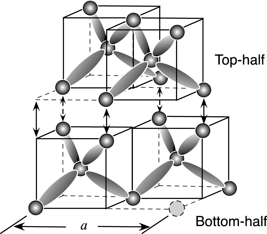
The other way of constructing the diamond lattice is to use four tetrahedral structures (Fig. 2.25a) as building blocks within a unit cell. As shown in Fig. 2.28, the bottom half of the unit cell is formed by joining two tetrahedral structures diagonally. The top half of the unit cell has the same arrangement but is rotated 90° with respect to the bottom half diagonal.
../images/325043_1_En_2_Chapter/325043_1_En_2_Fig28_HTML.png
Fig. 2.28

Construction of a diamond lattice structure using tetrahedral structures as building blocks

2.4.2 Zinc-Blende Structure

The zinc-blende crystal structure is closely related to the diamond structure. The only difference is that in zinc-blende structures, there are two different types of atoms in the lattice. As shown in Fig. 2.29, the two different atoms occupy alternating lattice sites. In each tetrahedral cubic structure, the center atom is different from the atoms located at corners.
../images/325043_1_En_2_Chapter/325043_1_En_2_Fig29_HTML.png
Fig. 2.29

Zinc-blende crystal structure. Two types of atoms are arranged alternately with each atom surrounded by four nearest neighbors of different types of atoms

The diamond structure of elemental semiconductors has the highest symmetry among all semiconductors. However, it lacks many of the symmetrical features enjoyed by primitive cubic. Compared to the diamond crystal structure, the symmetry of zinc-blende structure is further reduced. The physical structures of (111) and ($$ \bar{1}\bar{1}\bar{1} $$) surfaces are the same for diamond structure but different for zinc-blende crystal. For example, in GaAs the (111) consists entirely of Ga atoms, while ($$ \bar{1}\bar{1}\bar{1} $$) is a sheet of As atoms. Because of the different surface constituents, these two types of surface show very different chemical properties. Further, due to the nature of partially ionic bonding in zinc-blende structure, electric dipoles exist between the neighboring Ga and As atoms along 〈111〉. Although, at equilibrium, the net internal electric field is zero as the individual dipole moments get canceled out, compressions along 〈111〉 will cause atoms to move closer and induce a net internal electric field. This piezoelectric effect in compound semiconductors enhances carrier scattering which reduces the carrier mobility. More detailed discussions on the physical properties of III–V compounds with zinc-blende structure will be given in Chap. 4.

2.4.3 Wurtzite Structure

The wurtzite structure has the same tetrahedral coordination as the zinc-blende structure. It is the disposition of second-nearest neighbors which produces a hexagonal crystal. Figure 2.30 shows the unit cell of the hexagonal close-packed (HCP) structure. The basic HCP is formed by interlacing two basic hexagonal structures along the c-axis. The second hexagonal lattice is displaced from the first by c/2 along the c-axis and by 2a/3 and a/3 in the a1- and a2-directions, respectively. Only three atoms from the base of the second hexagonal are enclosed inside the first hexagonal unit cell. Each atom has twelve nearest neighbors: six in its own plane and three each in the planes above and below. The primitive unit cell has a rhombohedral structure as outlined. In the HCP structure, the c- and a-axes are related by $$ c = 2a\sqrt {2/3} $$.
../images/325043_1_En_2_Chapter/325043_1_En_2_Fig30_HTML.png
Fig. 2.30

Unit cell of the hexagonal close-packed (HCP) structure. The three atoms from the second hexagonal inside the unit cell are shown as dark spheres. The primitive cell is outlined and defined by unit vectors a1, a2, and c
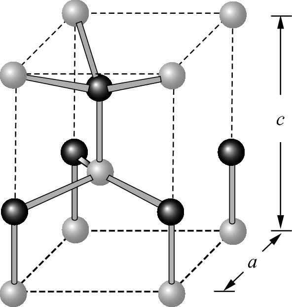
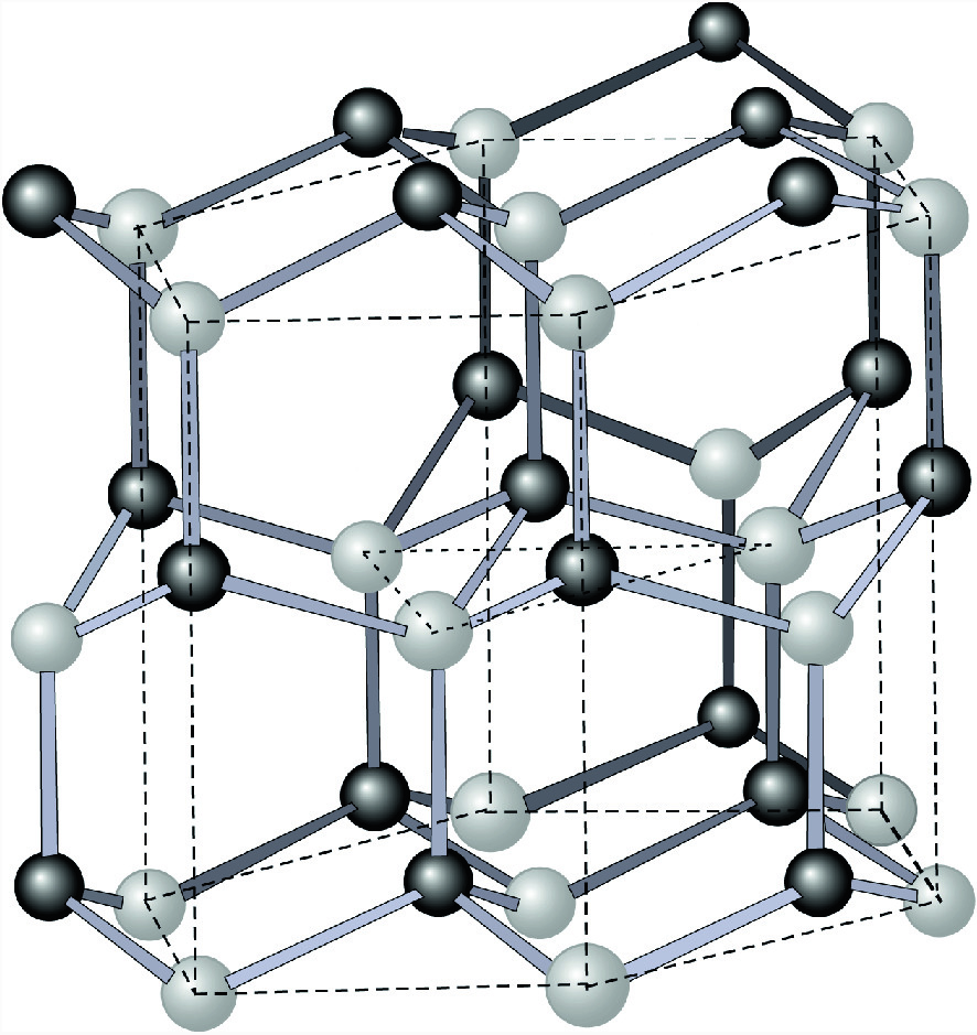
The wurtzite structure is formed by interlacing two identical HCP structures containing different atoms, e.g., group-III (Ga) and group-V (N) atoms, respectively, along c-axis. The displacement of the two lattices is the bond length of 3c/8. This arrangement of atoms can be seen from the primitive unit cell structure illustrated in Fig. 2.31. The hexagonal unit cell of a wurtzite crystal structure is shown in Fig. 2.32. It is clear that along the c-axis, layers containing atom A and atom B are staggered similarly to the (111) surface in the zinc-blende structure.
../images/325043_1_En_2_Chapter/325043_1_En_2_Fig31_HTML.png
Fig. 2.31

Primitive unit cell of the wurtzite structure
../images/325043_1_En_2_Chapter/325043_1_En_2_Fig32_HTML.png
Fig. 2.32

Unit cell of the wurtzite structure. The hexagonal boundary is outlined with dashed lines
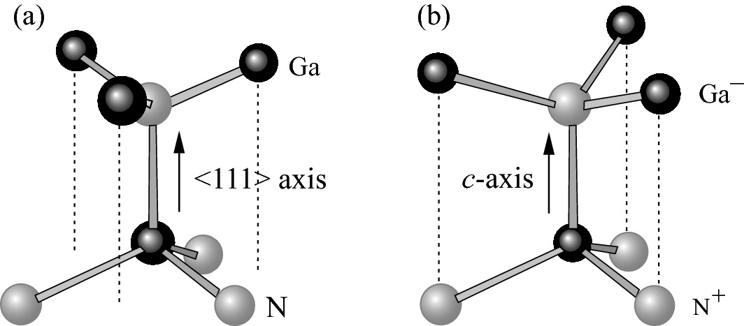
Next, we shall investigate why the nearest-neighbor atomic arrangement is the same for both zinc-blende and wurtzite structures but different for the second-nearest neighbors. In both structures, the bonds are covalent in nature with a certain fraction of ionicity. For zinc-blende crystals, the electron–electron repulsive force dominates the bond-forming mechanism, leading to the tetrahedral structure. The second nearest neighbors are also arranged by optimizing the repulsive forces between atoms. As shown in Fig. 2.33a, using zinc-blende 〈111〉 GaN as an example, the second-nearest Ga atoms in the top (111) plane are positioned in between the N atoms in the lower (111) plane. The two types of atoms in the neighboring (111) planes tend to minimize the repulsive force by maximizing the separation. For the wurtzite GaN structure, the high fraction of ionicity (0.5) implies that atoms are more ionized into Ga and N+. As shown in Fig. 2.33b, the cations and the anions tend to align along the c-axis by the strong Coulomb attraction force. Therefore, the preferred crystal structure of GaN is the wurtzite structure.
../images/325043_1_En_2_Chapter/325043_1_En_2_Fig33_HTML.png
Fig. 2.33

Second-nearest-neighbor bond arrangements along a 〈111〉 axis in zinc-blende and b c-axis in wurtzite GaN crystals

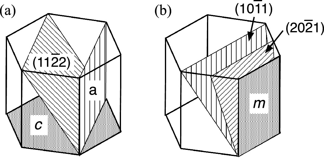
The layered structures shown in Fig. 2.33 containing atom A and atom B are similar in that they are staggered along the c-axis and the 〈111〉 axis in wurtzite structure and zinc-blende structure, respectively. But the similarity stops here. The alignment of cations and anions along the c-axis in wurtzite crystals such as GaN can easily induce a piezoelectric field by a mechanical stress applied along the same direction. The relative movements between cations and anions, caused by lattice vibrations above finite temperatures, break the equilibrium of the total electric field of the system. A net spontaneous polarization electric field is induced in the crystal along the c-axis. Thus, the (0001) c-plane is a polar surface. However, for some crystal planes containing mixed anions and cations that have equal numbers of bonds pointing out of the plane, e.g., $$ \left( {1\bar{1}00} \right) $$ m-plane and $$ \left( {11\bar{2}0} \right) $$ a-plane, the net spontaneous polarization field is zero. These are non-polar planes with c-axis parallel to the layer surface as shown in Fig. 2.34. Any crystal plane inclined between a non-polar plane and c-plane is a semi-polar plane including $$ \left( {10\bar{1}1} \right), \left( {11\bar{2}2} \right) $$ and $$ \left( {20\bar{2}1} \right). $$
../images/325043_1_En_2_Chapter/325043_1_En_2_Fig34_HTML.png
Fig. 2.34

Non-polar and semi-polar crystal planes in wurtzite III-N crystals. a $$ \left( {11\bar{2}0} \right) $$ a plane and $$ \left( {11\bar{2}2} \right) $$ semi-polar plane and b $$ \left( {1\bar{1}00} \right) $$ m-plane and $$ \left( {10\bar{1}1} \right) $$ and $$ \left( {20\bar{2}1} \right) $$ semi-polar planes

2.5 Reciprocal Lattice, Diffraction Condition, and Brillouin Zone

2.5.1 Crystal Diffraction

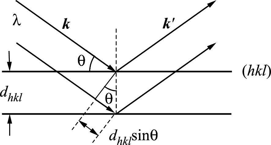
The lattice structure of a crystal can be deduced by diffraction experiments using radiation of a wavelength comparable with lattice dimensions. X-rays with proper energy are widely used as the diffraction sources to study semiconductor crystals. A suitable combination of X-ray wavelength λ and incident angle θ will enhance the diffraction according to Bragg’s law
$$ n\lambda = 2d_{hkl} \sin \theta $$
(2.29)
where dhkl is the lattice spacing and n is an integer (Fig. 2.35). Thus X-rays of a single wavelength directed on a crystal at an arbitrary angle will not be reflected. Currently, the two most widely used X-ray diffraction techniques are the following: The Laue method utilizes X-rays of many wavelengths at a single angle of incidence, and the rotating crystal method allows monochromatic rays to encounter the crystal at a variety of angles.
../images/325043_1_En_2_Chapter/325043_1_En_2_Fig35_HTML.png
Fig. 2.35

Reflection of a parallel beam of X-rays from two adjacent (hkl) planes of atoms in a crystal. The path difference between two X-rays has to be an integer multiplication of the path difference of 2dhkl sin θ for constructive reinforcement
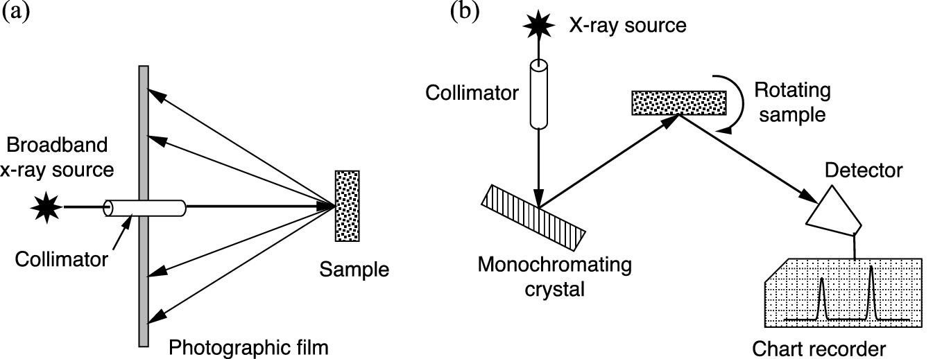
The Laue method uses a narrow beam of broadband X-rays to shine on a single crystal as shown in Fig. 2.36a. A diffraction beam will emerge for any X-ray wavelength satisfying the Bragg condition. All backscattered diffraction beams are recorded simultaneously in the photographic plate positioned between the crystal and the X-ray source. Each recorded diffraction ‘spot’ represents a specific wavelength that fits the Bragg condition. Therefore the crystal structure information recorded in the photographic plate is in the frequency domain. On the other hand, the rotating crystal method, shown in Fig. 2.36b, uses a monochromatic X-ray beam, shaped from a broadband source through multiple Bragg reflections from separate crystals, as the diffraction source on a crystal rotating at a constant speed. At any rotation angle θ that fulfills the Bragg condition, a diffraction beam emerges. Since the orientation (θ) of the crystal is varying as a function of time, the diffraction beams are recorded as ‘peaks’ in the time domain. For the same crystal subjected to diffraction measurements using both Laue and rotating crystal methods, the different diffraction results presented in the frequency and time domains are equivalent. In fact, because the frequency (f = 1/t) is the inverse of time (t), the Fourier transform allows us to convert diffraction results from time to frequency domains, and vice versa. Just as a time-varying quantity can be described as a sum of Fourier components in the frequency domain, so the spatial properties of a crystal can be described as the sum of Fourier components in Fourier space, known as the reciprocal space which has a dimension of length–1. This leads to the concept of the reciprocal lattice. In the discussion that follows, we shall see that the reciprocal lattices are associated with the Bragg diffraction condition in a crystal. Later in Chap. 3 we will apply the Fourier transformation to associate wave functions in real space (in length) and momentum space (in length–1).
../images/325043_1_En_2_Chapter/325043_1_En_2_Fig36_HTML.png
Fig. 2.36

a Laue diffraction method arrangement using broadband X-ray source. b A rotating crystal X-ray diffraction arrangement using monochromatic X-rays selected by Bragg reflection from a separate single crystal

2.5.2 Reciprocal Lattice

So far we have described the crystal structure in terms of the real-space lattice points of atomic positions. However, to understand the wave diffractions by crystals, as described in the last section, it is more convenient to describe the crystal structure from the point of view of crystal planes. A set of (hkl) planes of the crystal structure is completely specified by the unit vector of the plane n and the inter-plane spacing dhkl. The overall structure of the crystal is then completely specified by the set of values of n and dhkl. This specific way of relating crystal structures to values of n and dhkl is cumbersome. Conversely, a much more useful representation is to define a vector which uniquely relates to each set of n and dhkl of the real-space lattice points
$$ \varvec{G}_{hkl} = 2\pi \varvec{n}/d_{hkl} $$
(2.30)

It is obvious that this vector has the dimension of inverse length and can be used to define the so-called reciprocal lattice. Thus, every crystal structure has both a real-space lattice and a reciprocal lattice associated with it.

To further explore the concept of reciprocal lattice vectors, the interactions of a wave with a periodic physical quantity of a crystal are illustrated below. In crystal diffraction measurements, the condition for the constructive interference of a wave scattered from the lattice points depends on the detailed unit cell structure of the crystal. Thus, the scattering intensity of the incident wave is determined by the spatial distribution of atoms within each cell. In periodic lattice structures, Fourier transformation can be applied to relate the direct lattice and wave vector domains. In a 1D system of a periodic lattice with a period a along x, the scattering wave density ρ satisfies the condition
$$ \rho \left( {x + a} \right) = \rho \left( x \right) $$
(2.31)
Using Fourier transformation, the 1D wave density becomes
$$ \rho \left( x \right) = \frac{{a_{0} }}{2} + \mathop \sum \limits_{n = 1}^{\infty } \left( {a_{n} \cos \frac{2n\pi }{a}x + b_{n} \sin \frac{2n\pi }{a}x} \right) = \mathop \sum \limits_{ - \infty }^{\infty } c_{n} \exp \left( {i\frac{2n\pi }{a}x} \right) $$
(2.32)
where
$$ c_{n} = \frac{1}{a}\mathop \int \limits_{ - a/2}^{a/2} \rho \left( x \right)\exp \left( { - i\frac{2n\pi }{a}x} \right){\text{d}}x $$
(2.33)
is the Fourier coefficient. A displacement of x = ma, where m is an integer, leads to an identical ρ(x), hence satisfying the periodic requirement. Assume 2π/a ≡ |k| is the wave vector associated with the direct lattice spacing a. The 1D scattering wave density is expressed in terms of the wave vector k and the lattice vector x by
$$ \rho \left( x \right) = \mathop \sum \limits_{ - \infty }^{\infty } c_{n} \exp \left( {in\varvec{k} \cdot \varvec{x}} \right) $$
(2.34)
In 3D periodic systems,
$$ \rho \left( {\varvec{r} + \varvec{T}} \right) = \rho \left( \varvec{r} \right) $$
(2.35)
where $$ \varvec{T} = h^{\prime}\varvec{a} + k^{\prime}\varvec{b} + l^{\prime}\varvec{c} $$ is the translation vector. We can use the same equation with a minor modification as shown below:
$$ \rho \left( r \right) = \mathop \sum \limits_{n} c_{G} \exp \left( {i\varvec{G} \cdot \varvec{r}_{n} } \right) $$
(2.36)
The wave vector k and lattice vector x are replaced by G and rn, respectively. In order to preserve the translation invariance of ρ(r) with respect to the lattice vector rn, the vector G must fulfill certain conditions. Just like the 1D case, the product of G and rn has to preserve the periodic property of the lattice. Thus,
$$ \varvec{G} \cdot \varvec{r}_{n} = 2m\pi \;{\text{and}}\;\varvec{r}_{n} = n_{1} \varvec{a} + n_{2} \varvec{b} + n_{3} \varvec{c} $$
(2.37)
where m is an integer for all n1, n2, and n3, and a, b, c are the unit vectors of the lattice. Assume vector G can be expressed as
$$ \varvec{G} = h\varvec{a}^{*} + kb^{*} + l\varvec{c}^{*} $$
(2.38)
where h, k, l are integers and a*, b*, c* are unit vectors of a different coordination system. Then
$$ \varvec{G} \cdot \varvec{r}_{n} = \left( {h\varvec{a}^{*} + k\varvec{b}^{*} + l\varvec{c}^{*} } \right) \cdot \left( {n_{1} \varvec{a} + n_{2} \varvec{b} + n_{3} \varvec{c}} \right) = 2m\pi $$
The relations between a, b, c and a*, b*, c* are derived as follows. For example, in the case of n2 = n3 = 0, we have
$$ \varvec{G} \cdot \varvec{r}_{n} = n_{1} \left( {h\varvec{a} \cdot \varvec{a}^{*} + k\varvec{a} \cdot \varvec{b}^{*} + l\varvec{a} \cdot \varvec{c}^{*} } \right) = 2m\pi $$
For an arbitrary choice of n1, this can only be satisfied by
$$ \varvec{a} \cdot \varvec{a}^{*} = 2\pi \,{\text{and}}\,\varvec{a} \cdot \varvec{b}^{*} = \varvec{a} \cdot \varvec{c}^{*} = 0 $$
This implies a general expression of
$$ \varvec{G}_{i} \cdot \varvec{r}_{j} = 2\pi \delta_{ij} $$
(2.39)
where Gi and rj are the ith and jth components of vectors G and rn, respectively, and
$$ \delta_{ij} = \left\{ {\begin{array}{*{20}l} {1\; {\text{for }}\;i = j} \hfill \\ {0\,{\text{for}}\; i \ne j} \hfill \\ \end{array} } \right. $$
(2.40)
The conditions stated above of a · a* = 2π and a · b* = a · c* = 0 imply a* = k1(b × c), or a* is perpendicular to the plane containing b and c. Therefore
$$ \varvec{a} \cdot \varvec{a}^{*} = 2\pi = k_{1} \left( {\varvec{a} \cdot \varvec{b} \times \varvec{c}} \right) $$
and
$$ k_{1} = \frac{2\pi }{{\left( {\varvec{a} \cdot \varvec{b} \times \varvec{c}} \right)}} $$
(2.41)
This leads to the definition of the reciprocal lattice unit vectors a*, b*, and c*,
$$ \left\{ {\begin{array}{*{20}c} {\varvec{a}^{*} = 2\pi \displaystyle{\frac{{\varvec{b} \times \varvec{c}}}{{\left( {\varvec{a} \cdot \varvec{b} \times \varvec{c}} \right)}}}} \\ {\varvec{b}^{*} = 2\pi \displaystyle{\frac{{\varvec{c} \times \varvec{a}}}{{\left( {\varvec{a} \cdot \varvec{b} \times \varvec{c}} \right)}}}} \\ {\varvec{c}^{*} = 2\pi \displaystyle{\frac{{\varvec{a} \times \varvec{b}}}{{\left( {\varvec{a} \cdot \varvec{b} \times \varvec{c}} \right)}}}} \\ \end{array} } \right. $$
(2.42)
and G = ha* + kb* + lc* is the reciprocal lattice vector.
Whether this G satisfies the periodicity requirement can be examined by using the following example. Assuming G is the solution, it should possess the periodic property of
$$ \begin{aligned} \rho \left( {\varvec{r} + \varvec{T}} \right) = \mathop \sum \limits_{G} c_{G} \exp \left( {i\varvec{G} \cdot \varvec{r}} \right)exp\left( {i\varvec{G} \cdot \varvec{T}} \right) = \rho \left( \varvec{r} \right) \quad \quad \quad \quad \quad \quad \qquad \qquad \qquad \quad & \\ \exp \left( {i\varvec{G} \cdot \varvec{T}} \right) = \exp \left[ {i\left( {hh^{\prime} + kk^{\prime} + ll^{\prime}} \right)} \right] = \exp \left( {iu} \right) = { \sin }\left( {2u\pi } \right) \qquad \qquad \qquad \quad  &  \\  + { \cos }\left( {2u\pi } \right) = 1 \qquad \qquad \qquad \quad  \\ \end{aligned} $$
where u = (hh′ + kk′ + ll′) = integer. Thus,
$$ \rho \left( {\varvec{r} + \varvec{T}} \right) = \mathop \sum \limits_{G} c_{G} \exp \left( {i\varvec{G} \cdot \varvec{r}} \right) = \rho \left( \varvec{r} \right) $$
(2.43)

The periodicity is maintained in the 3D reciprocal lattice.

2.5.3 Properties of the Reciprocal Lattice Vector
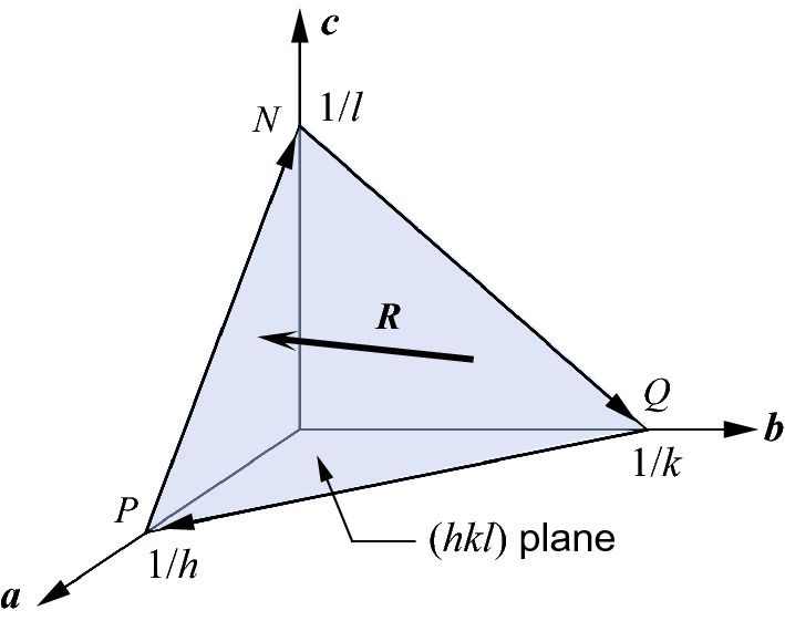
As shown in Fig. 2.37, in direct lattice, the (hkl) plane intersects with a-, b-, and c-axes at 1/h, 1/k, and 1/l, respectively. The three position vectors extending from the origin to these three intersections are a/h, b/k, and c/l. Using these three vectors, we can define three vectors lying along the edges of the (hkl) plane as indicated by
../images/325043_1_En_2_Chapter/325043_1_En_2_Fig37_HTML.png
Fig. 2.37

Geometry of the direct lattice (hkl) plane and related vectors

$$ \varvec{QP} = \left( {\frac{\varvec{a}}{h} - \frac{\varvec{b}}{k}} \right),\varvec{PN} = \left( {\frac{\varvec{a}}{h} - \frac{\varvec{c}}{l}} \right), \,{\text{and}}\,\varvec{NQ} = \left( {\frac{\varvec{b}}{k} - \frac{\varvec{c}}{l}} \right) $$
A linear combination of the above three vectors (QP × D + PN × E + NQ × F) forms a general vector R lying in the (hkl) plane:
$$ \varvec{R} = \frac{\varvec{a}}{h}\left( {D - E} \right) + \frac{\varvec{b}}{k}\left( {F - D} \right) + \frac{\varvec{c}}{l}\left( {E - F} \right) $$
(2.44)
where D, E, and F are integers. It can be further simplified by assuming A = D − E, B = F − D, C = E − F, and A + B + C = 0. Thus,
$$ \varvec{R} = A\left( {\frac{\varvec{a}}{h}} \right) + B\left( {\frac{\varvec{b}}{k}} \right) + C\left( {\frac{\varvec{c}}{l}} \right) = \left( {\frac{A}{h}} \right)\varvec{a} + \left( {\frac{B}{k}} \right)\varvec{b} + \left( {\frac{C}{l}} \right)\varvec{c} $$
(2.45)
$$ \begin{aligned} \varvec{R} \cdot \varvec{G}_{hkl} & = \left[ {\left( {\frac{A}{h}} \right)\varvec{a} + \left( {\frac{B}{k}} \right)\varvec{b} + \left( {\frac{C}{l}} \right)\varvec{c}} \right] \cdot \left( {h\varvec{a}^{*} + k\varvec{b}^{*} + l\varvec{c}^{*} } \right) \\ & \quad = \left( {\frac{A}{h}} \right)h + \left( {\frac{B}{k}} \right)k + \left( {\frac{C}{l}} \right)l = A + B + C = 0 \\ \end{aligned} $$
(2.46)

Therefore, RGhkl. The reciprocal lattice vector defined by Ghkl = ha* + kb* + lc* lies perpendicular to the direct lattice (hkl) plane.
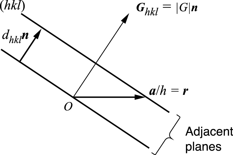
We now show that with the aid of Fig. 2.38 the separation of the planes in the direct lattice dhkl is equal to 2π/Ghkl.
../images/325043_1_En_2_Chapter/325043_1_En_2_Fig38_HTML.png
Fig. 2.38

Construction for the determination of the spacing between successive (hkl) planes. n is the surface normal unit vector

$$ d_{hkl} = \varvec{r} \cdot \varvec{n} = \varvec{r} \cdot \frac{{\varvec{G}_{hkl} }}{{\left| {\varvec{G}_{hkl} } \right|}} = \frac{\varvec{a}}{h} \cdot \frac{{h\varvec{a}^{*} + k\varvec{b}^{*} + l\varvec{c}^{*} }}{{\left| {\varvec{G}_{hkl} } \right|}} = \frac{2\pi }{{\left| {\varvec{G}_{hkl} } \right|}} $$
(2.47)
The perpendicular distance of the adjacent (hkl) planes is
$$ d_{hkl} = \frac{2\pi }{{\left| {G_{hkl} } \right|}}\,{\text{or}}\,d_{hkl} = \frac{2\pi }{{\sqrt {h^{2} + k^{2} + l^{2} } }} $$
(2.48)

2.5.4 Diffraction Condition

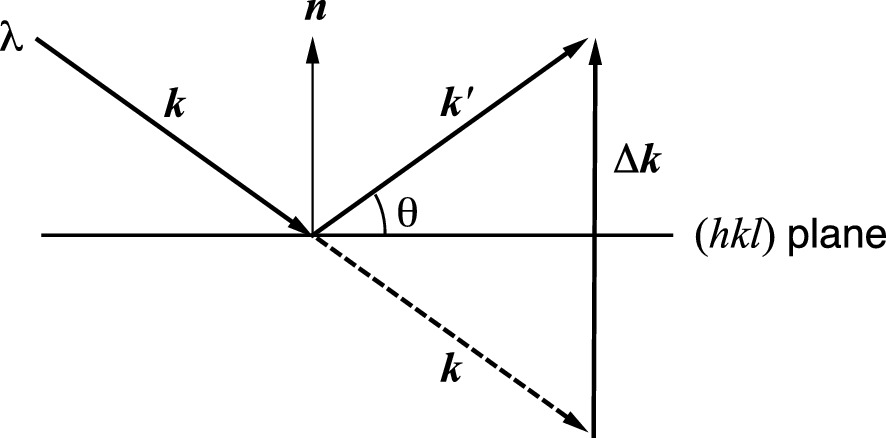
From Fig. 2.35, the Bragg law of diffraction (2.29) requires  = 2dhkl sin θ. It is also possible to express the diffraction condition with the reciprocal lattice vector. Instead of considering the wavelength λ of the radiation which interacts with the crystal, we shall now consider the initial and final wave vectors k, k′ of a reflected diffraction. Assume a wave vector k associated with a wavelength λ is incident on the (hkl) plane and encounters an elastic diffraction or elastic scattering where there is no change in λ. Therefore, the diffracted wave vector
$$ \left| {\varvec{k}^{\prime}} \right| = \left| \varvec{k} \right| = 2\pi /\lambda $$
(2.49)
The change of k, shown in Fig. 2.39, is
../images/325043_1_En_2_Chapter/325043_1_En_2_Fig39_HTML.png
Fig. 2.39

The change in wave vector when undergoing an elastic scattering at the (hkl) plane

$$ \Delta \varvec{k} = \varvec{k}^{\prime } - \varvec{k} = 2\left| \varvec{k} \right|\varvec{n}\sin \theta = \left( {\frac{4\pi }{\lambda }{ \sin }\theta } \right)\varvec{n} = \left( {\frac{4\pi }{\lambda }\sin \theta } \right)\frac{{\varvec{G}_{hkl} }}{{\left| {\varvec{G}_{hkl} } \right|}} $$
(2.50)

The change Δk is in the direction of the surface normal and perpendicular to the (hkl) planes.

Since dhkl = 2π/|Ghkl| and 2d sin θ = , then
$$ \Delta \varvec{k} = \left( {\frac{{2d_{hkl} }}{\lambda }{ \sin }\theta } \right)\varvec{G}_{hkl} $$
(2.51)
$$ \Delta \varvec{k} = \varvec{G}_{hkl} $$
(2.52)
or
$$ \varvec{k^{\prime}} = \varvec{k} + \varvec{G}_{hkl} $$
(2.53)

Thus the scattering vector Δk is equal to a reciprocal lattice vector Ghkl. This is the 3D Bragg diffraction condition.
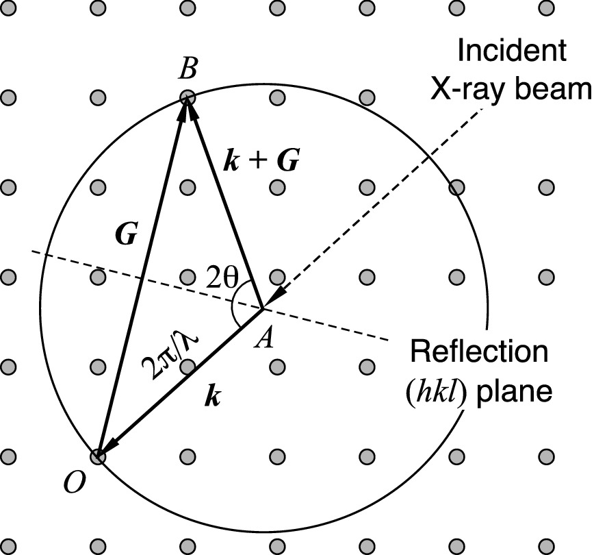
In the Laue method of Fig. 2.36a, the array of diffraction spots from a crystal, recorded on the photographic film, thus corresponds to the set of points generated by Ghkl in the reciprocal lattice space. This can be represented graphically by the Ewald sphere construction shown in Fig. 2.40. We start by drawing a vector corresponding to the incident X-ray beam, whose length is 2π/λ and which terminates at a point O of the reciprocal lattice. Note that the tail of the vector AO does not necessarily have to rest on a reciprocal lattice point. A sphere with a radius |k| or 2π/λ is constructed about point A as the center. The diffraction condition is satisfied whenever the spherical surface coincides with points of the reciprocal lattice where k′ = k + Ghkl. The vector OB or Ghkl that connects the two reciprocal lattice points coinciding with the sphere must be normal to the (hkl) plane of the direct lattice. Using simple trigonometric relations, we can verify in the following that Ghkl satisfies the Bragg condition. From (2.48), Ghkl has a length 2/dhkl, where n is an integer. From Fig. 2.40, the length OB can also be expressed as 4πsin θ/λ. Equating these two expressions for the length of the vector OB leads to the Bragg condition.
../images/325043_1_En_2_Chapter/325043_1_En_2_Fig40_HTML.png
Fig. 2.40

Ewald construction for the Laue diffraction condition from a crystal in the reciprocal lattice. The incident X-ray beam has a wavelength λ

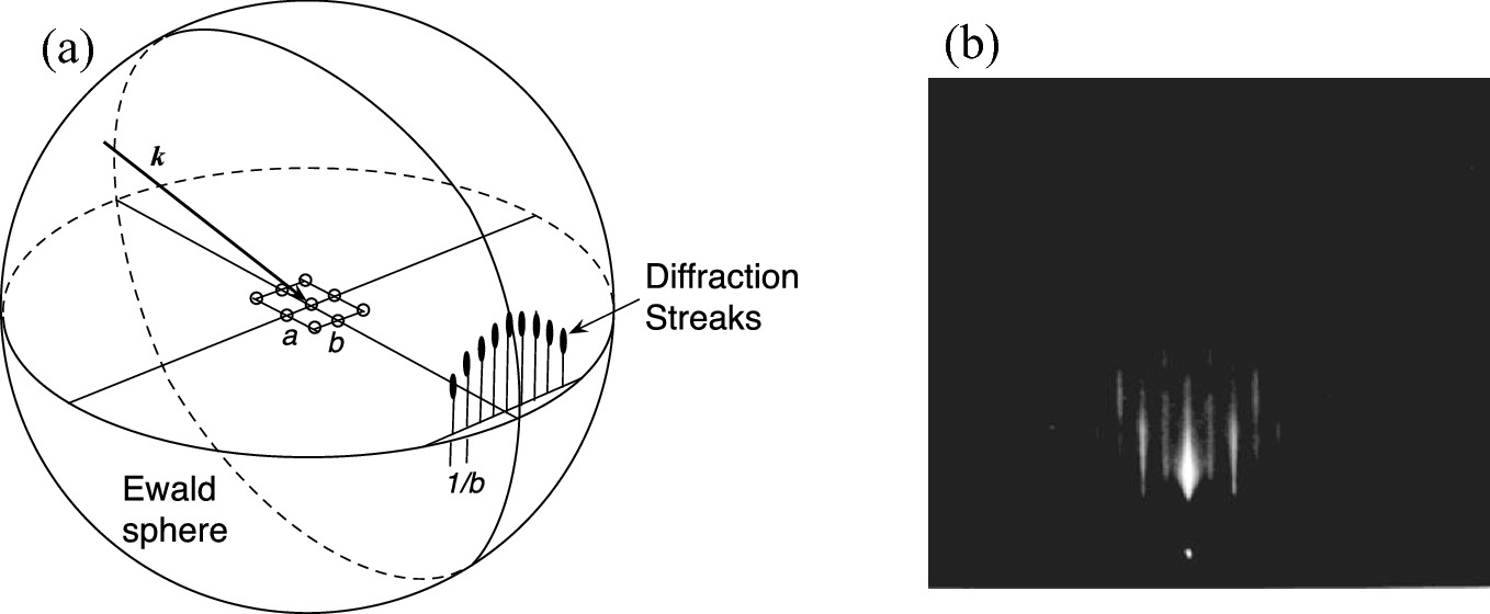
The diffraction condition of a real crystal surface can also be correlated to the reciprocal lattice using the Ewald sphere construction scheme. For example, the reflection high-energy electron diffraction (RHEED) method is commonly used to study crystal surfaces as shown in Fig. 2.41. Electrons having energy of 5–30 keV, corresponding to an electron wavelength of less than the lattice constant, are incident on the crystal surface at a low glancing angle of ≤5°. The diffraction of the incoming primary electron beam by the two-dimensional (2D) atomic network of surface atoms leads to the appearance of streaks normal to the shadow edge on the fluorescence screen. The conditions for constructive interference of the elastically scattered electrons may be inferred using the Ewald sphere construction in the reciprocal lattice. Due to the loss of periodicity in the dimension above the crystal surface, the surface layer is represented by rods in a direction normal to the real surface in the reciprocal space (Fig. 2.42). The reciprocal lattice rods are labeled with only two Miller indices, h and k. Diffraction occurs where the Ewald sphere cuts a reciprocal lattice rod and the diffraction beam is labeled with the Miller index (hk) of the rod causing it. It should be noted that due to the high electron acceleration energy, the radius of the Ewald sphere is much larger than the separation of the rods. The wavelength of the incident electron beam λ is related to the energy by
../images/325043_1_En_2_Chapter/325043_1_En_2_Fig41_HTML.png
Fig. 2.41

Schematic diagram of the RHEED arrangement showing the incident electron beam at an angle θ ≤ 5° to the sample surface. The elongated spots indicate the intersection of the Ewald sphere with diffraction rods. (Reprint with permission from [3], copyright AIP Publishing.)
../images/325043_1_En_2_Chapter/325043_1_En_2_Fig42_HTML.png
Fig. 2.42

a Ewald sphere construction for a reconstructed semiconductor surface in reciprocal lattice space. The real-space lattice atoms are shown as circles. (Reprint with permission from [4], copyright Elsevier) b Diffraction pattern from the GaAs (001) − (2 × 4) surface along the $$ \left[ {\bar{1}\bar{1}0} \right] $$ azimuth

$$ E = \frac{{\hbar^{2} }}{2m}\left( {\frac{2\pi }{\lambda }} \right)^{2} $$
(2.54)

Thus, at 5 keV, λ = 0.0174 nm. The radius of the Ewald sphere is |k| = 2π/λ = 362 nm−1. If the surface lattice network has a lattice constant a of 5 Å, then the distance between adjacent rods in reciprocal space will be 2π/a = 12.57 nm−1. As a result, the intersection of the nearly flat Ewald sphere and rods occurs along their length, resulting in a streaked diffraction pattern as illustrated in Fig. 2.42a. However, due to the finite surface roughness, the short diffraction streaks transform into elongated lines. Figure 2.42b is a typical RHEED pattern for a smooth (001) surface of GaAs.

2.5.5 The Brillouin Zone

An alternative expression of the Bragg diffraction condition can be derived by rewriting (2.53) as
$$ \left( {\varvec{k}^{\prime}} \right)^{2} = \left( {\varvec{k} + \varvec{G}} \right)^{2} $$
(2.55)
or
$$ \left( {k^{\prime}} \right)^{2} = k^{2} + G^{2} + 2\varvec{k} \cdot \varvec{G} $$
(2.56)
Since |k| = |k′|, (2.56) can be expressed as
$$ 2\varvec{k} \cdot \varvec{G} + G^{2} = 0 $$
(2.57)
or
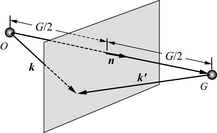
$$ \varvec{k} \cdot \left( {\varvec{G}/G} \right) = \varvec{k} \cdot \varvec{n} = G/2 $$
(2.58)
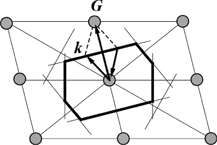
Equation (2.58) corresponds to a geometric structure that describes the locus of all points satisfying the Bragg condition, called the Bragg plane (Fig. 2.43). This is a plane that is the perpendicular bisector of a reciprocal lattice vector G. The Bragg law is only satisfied for those incident wave vectors whose tips lie on the Bragg plane in reciprocal space when the vector origin is tied to a reciprocal lattice point. Since the reciprocal lattice of a periodic direct lattice is also periodic and infinite in extent, it is most useful only to require the use of a limited volume of reciprocal lattice, or k-space. This volume is called the first Brillouin zone. The Bragg plane simply forms one of the faces of the first Brillouin zone. As shown in Fig. 2.44, the smallest 2D polyhedron centered at the origin and enclosed by perpendicular bisectors of reciprocal lattice vectors, i.e., Bragg planes, forms the (first) Brillouin zone.
../images/325043_1_En_2_Chapter/325043_1_En_2_Fig43_HTML.png
Fig. 2.43

Geometrical representation of the Bragg diffraction condition. Diffraction only occurs for an incident wave vector whose tip lies on the Bragg plane if its origin is tied to a reciprocal lattice point
../images/325043_1_En_2_Chapter/325043_1_En_2_Fig44_HTML.png
Fig. 2.44

First Brillouin zone formed in the reciprocal space for a 2D oblique lattice. It is shown bisecting the midpoints of six shortest reciprocal lattice vectors from the center of this lattice structure

The points on the Brillouin zone boundary are special because every wave with k extending from the origin to the zone boundary gives rise to a Bragg reflected wave. It is obvious from Fig. 2.43 that k′ = k + G is satisfied on these boundaries. The interference of the incident primary waves and the Bragg reflected waves produces a ‘standing wave.’ This is important for the understanding of X-ray diffraction and the formation of a bandgap in the electronic structure of semiconductor materials.
  1. (a)

    Example for a 2D square lattice

     
The reciprocal lattice of a square direct lattice, whose lattice spacing is a, is also a square lattice of spacing 1/a (Fig. 2.45). The reciprocal lattice vector pointing from the origin to a lattice point (u, v) can be expressed as G = (2π/a)(uix + viy) where u and v are integers. According to the Bragg condition, for k = kxix + kyiy
../images/325043_1_En_2_Chapter/325043_1_En_2_Fig45_HTML.png
Fig. 2.45

Construction of the first (dashed line boundary) and second (solid line boundary) Brillouin zones (BZ) in a 2D reciprocal lattice space. The square direct lattice has a lattice spacing a

$$ 2\varvec{k} \cdot \varvec{G} + G^{2} = \frac{4\pi }{a}\left( {uk_{x} + vk_{y} } \right) + \frac{{4\pi^{2} }}{{a^{2} }}\left( {u^{2} + v^{2} } \right) = 0 $$
(2.59a)
or
$$ f\left( {k_{x} ,k_{y} } \right) = uk_{x} + vk_{y} + \frac{\pi }{a}\left( {u^{2} + v^{2} } \right) = 0 $$
(2.59b)
This is a straight line of kx and ky. The intersections on the x- and y-axes are
$$ \left\{ {\begin{array}{*{20}l} {k_{x} = - \displaystyle{\frac{\pi }{a}}\left( {\displaystyle{\frac{{u^{2} + v^{2} }}{u}}} \right) \,{\text{on}}\,x{\text{-axis}}} \hfill \\ {k_{y} = - \displaystyle{\frac{\pi }{a}}\left( \displaystyle{{\frac{{u^{2} + v^{2} }}{v}}} \right)\,{\text{on}}\,y{\text{-axis}}} \hfill \\ \end{array} } \right. $$
(2.60)

To construct the smallest rectangle, we calculate kx and ky with the smallest possible u and v. At u = 0 and v = ± 1, we have ky = ± π/a. Similarly, at v = 0 and u = ± 1, we have kx = ± π/a. The four constant k’s form a square. This is the first Brillouin zone as shown in Fig. 2.45. Alternatively, bisecting the midpoints of four shortest reciprocal lattice vectors from the origin can also form the first Brillouin zone. For the second Brillouin zone, kx ± ky = ± 2π/a for u = ± 1 and v = ± 1. The higher-order Brillouin zones can be constructed through the same procedures. For example, using u = 0, v = ± 2 and v = 0, u = ± 2, the third zone boundaries are defined.

On the Brillouin zone boundary, the wave vectors must follow the Bragg condition. For example, the Bragg condition of the first Brillouin zone, n = 1, becomes
$$ 2a\sin \theta = \lambda $$
(2.61)
For an incident wave of a wavelength λ, as seen in Fig. 2.45, the wave vector is
$$ \left| \varvec{k} \right| = \sqrt {k_{0}^{2} + \left( {\frac{\pi }{a}} \right)^{2} } = \frac{2\pi }{\lambda } $$
(2.62)
and
$$ \sin \theta = \frac{{k_{y} }}{{\sqrt {k_{x}^{2} + k_{y}^{2} } }} = \frac{\pi /a}{{\sqrt {k_{0}^{2} + \left( {\pi /a} \right)^{2} } }} = \frac{2\pi }{{\sqrt {k_{0}^{2} + \left( {\pi /a} \right)^{2} } }} \cdot \frac{1/a}{2} = \frac{\lambda }{2a} $$
(2.63)

Thus, 2a sin θ = 2a · (λ/2a) = λ, fulfilling the Bragg law.

Therefore the Brillouin zone construction exhibits all the wave vectors that can be Bragg diffracted by the crystal. Other waves get weakened and eventually cease to exist.
  1. (b)

    3D Brillouin zone of a FCC crystal


As we will discuss in Chap. 3, the Brillouin zone concept is essential for the development of the energy band structure of semiconductors. The construction of Brillouin zones in 3D semiconductor crystals follows a procedure similar to that for the 2D case. Since most semiconductor crystals have either zinc-blende or wurtzite lattice structure, we shall investigate the Brillouin zones of the basic FCC and simple hexagonal structures.

First, we need to transform the primitive unit cell of the FCC structure into reciprocal lattice spacing. As shown in Fig. 2.46, the translation vectors which define the primitive unit cell of the FCC lattice are
../images/325043_1_En_2_Chapter/325043_1_En_2_Fig46_HTML.png
Fig. 2.46

Primitive unit cell of an FCC crystal structure is formed by three translation vectors a′, b′, and c′. These translation vectors point from the origin toward the surface atoms diagonally

$$ \varvec{a^{\prime}} = \left( {a/2} \right)\left( {\varvec{b} + \varvec{c}} \right),\varvec{ b}^{\prime} = \left( {a/2} \right)\left( {\varvec{c} + \varvec{a}} \right),\varvec{ c}^{\prime} = \left( {a/2} \right)\left( {\varvec{a} + \varvec{b}} \right) $$
(2.64)
where a/2 defines the size of the unit cell. The translation vectors a′, b′, and c′ are vectors pointing from the origin to three neighboring face-centered surface lattice points, respectively. The formed cubic volume of the primitive cell is a′ · b′ × c′ = a3/2$$ \sqrt 2 $$.
Then the primitive translation vectors in the reciprocal lattice are calculated following (2.42) as
$$ \left\{ {\begin{array}{*{20}l} {\varvec{a}^{*} = 2\pi \left( \displaystyle{{\frac{{\varvec{b}^{\prime} \times \varvec{c}^{\prime}}}{{\varvec{a}^{\prime} \cdot \varvec{b}^{\prime} \times \varvec{c}^{\prime}}}}} \right) = \displaystyle{\frac{{2\pi a^{2} \left( { - \varvec{a} + \varvec{b} + \varvec{c}} \right)/4}}{{a^{3} /4}}} = \displaystyle{\frac{2\pi }{a}}\left( { - \varvec{a} + \varvec{b} + \varvec{c}} \right)} \hfill \\ {\varvec{b}^{*} = 2\pi \left( \displaystyle{{\frac{{\varvec{c}^{\prime} \times \varvec{a}^{\prime}}}{{\varvec{a}^{\prime} \cdot \varvec{b}^{\prime} \times \varvec{c}^{\prime}}}}} \right) = \displaystyle{\frac{{2\pi a^{2} \left( {\varvec{a} - \varvec{b} + \varvec{c}} \right)/4}}{{a^{3} /4}}} = \displaystyle{\frac{2\pi }{a}}\left( {\varvec{a} - \varvec{b} + \varvec{c}} \right)      } \hfill \\ {\varvec{c}^{*} = 2\pi \left( \displaystyle{{\frac{{\varvec{a}^{\prime} \times \varvec{b}^{\prime}}}{{\varvec{a}^{\prime} \cdot \varvec{b}^{\prime} \times \varvec{c}^{\prime}}}}} \right) = \displaystyle{\frac{{2\pi a^{2} \left( {\varvec{a} + \varvec{b} - \varvec{c}} \right)/4}}{{a^{3} /4}}} = \displaystyle{\frac{2\pi }{a}}\left( {\varvec{a} + \varvec{b} - \varvec{c}} \right)      } \hfill \\ \end{array} } \right. $$
(2.65)
These are vectors oriented along the $$ \left[ {\bar{1}11} \right] $$, $$ \left[ {1\bar{1}1} \right] $$, and $$ \left[ {11\bar{1}} \right] $$] directions of a cubic lattice, respectively. We can plot (2.65) as shown in Fig. 2.47 and realize that these are the primitive translation vectors of a BCC lattice! Thus, the reciprocal of an FCC lattice is a BCC lattice. The volume of the primitive cell in the reciprocal lattice is a* · b* × c* = 4(2π/a)3.
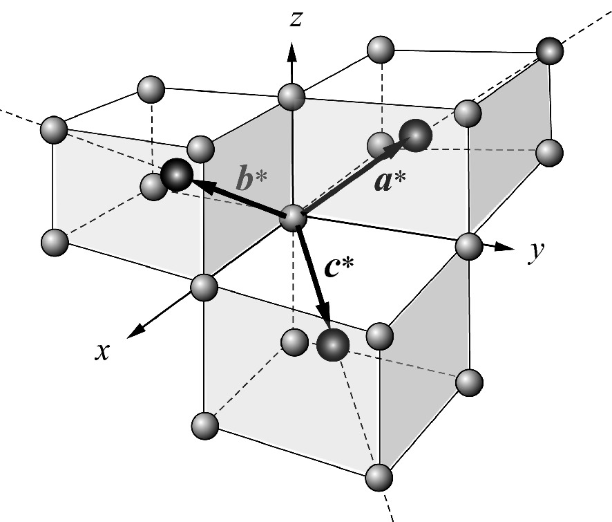
../images/325043_1_En_2_Chapter/325043_1_En_2_Fig47_HTML.png
Fig. 2.47

Reciprocal translation vectors a*, b*, and c* of the FCC crystal structure. The lattice points at the body centers are drawn as larger dark spheres

To construct the first Brillouin zone from these reciprocal translation vectors, we shall derive a general form of Ghkl:
$$ \varvec{G}_{hkl} = h\varvec{a}^{*} + k\varvec{b}^{*} + l\varvec{c}^{*} = \left( {\frac{2\pi }{a}} \right)\left[ {\left( { - h + k + l} \right)\varvec{a} + \left( {h - k + l} \right)\varvec{b} + \left( {h + k - l} \right)\varvec{c}} \right] $$
(2.66)
In a BCC lattice, there are eight nearest neighbors from the body-centered lattice point along 〈111〉 (Fig. 2.48). For h = k = l = ± 1, there are eight reciprocal lattice vectors pointing to each corner of the BCC structure. The boundaries of the first Brillouin zone are located at G/2, and
../images/325043_1_En_2_Chapter/325043_1_En_2_Fig48_HTML.png
Fig. 2.48

First Brillouin zone of the face-centered cubic lattice in reciprocal space. Six pyramid-shaped volumes (one shown in gray lines) are excluded since they are intersected by second nearest neighbors

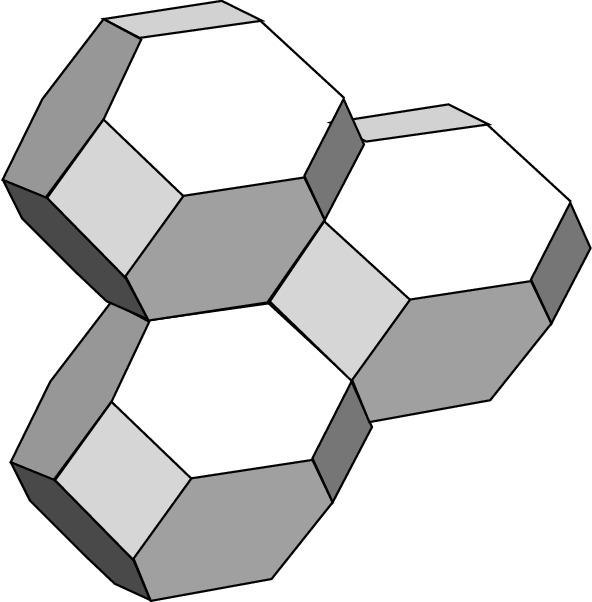
$$ \frac{1}{2}{\varvec{G}_{<111>}} = \frac{\pi }{{\varvec{d}_{<111>} }} = \frac{\pi }{a}\left( { \pm \varvec{a} \pm \varvec{b} \pm \varvec{c}} \right) $$
(2.67)
These eight vectors generate eight Brillouin zone surfaces halfway between the origin and the nearest points of the lattice, which form a regular octahedron. However, this is not the first Brillouin zone since the planes arising from the second nearest neighbors between body-center lattice points intersect it. Therefore, the six pyramid-shaped corners in the 〈100〉 directions extending outside the first zone are excluded. The final form of the first Brillouin zone for an FCC lattice becomes a truncated octahedron (Fig. 2.48). The volume enclosed by the first Brillouin zone is also known as the WignerSeitz primitive cell of the reciprocal lattice. The eight hexagonal faces arise from the planes halfway to the atoms at the corners, while the six smaller square faces are halfway to the atoms in the middle of the next cells. As expected, these unit cells can fit together to fill the whole space as demonstrated in Fig. 2.49.
../images/325043_1_En_2_Chapter/325043_1_En_2_Fig49_HTML.png
Fig. 2.49

Way in which the first Brillouin zone cells of an FCC lattice can fill the whole space

  1. (c)

    3D Brillouin zone of a simple hexagonal crystal

     
The reciprocal lattice of a simple hexagonal lattice is another simple hexagonal lattice rotated 30° about the c-axis. If the basic lattice translations for the direct lattice in the basal plane and along the c-axis are, respectively, a and c, then for the reciprocal lattice they are a* and c*, where a* = $$ 4\pi /\sqrt 3 a $$ and c* = 2π/c. Figure 2.50 shows seven points of the reciprocal lattice of a simple hexagonal lattice. If we take the central point O as origin, the other six lie at the corners of a regular hexagon of side a* = $$ 4\pi /\sqrt 3 a $$ and are the six nearest neighbors. The first Brillouin zone is formed by connecting bisectors of the lines joining O to the other six nearest neighbors. It is a hexagon whose sides have length $$ a^{*} /\sqrt 3 $$ = 4π/3a and hence covers a unit cell area of $$ \left( {a^{*} } \right)^{2} \sqrt 3 /2 $$ = $$ 8\pi^{2} /\sqrt 3 a^{2} $$. It should be noted that the hexagon forming the first Brillouin zone has the same orientation as the hexagons of the direct lattice.
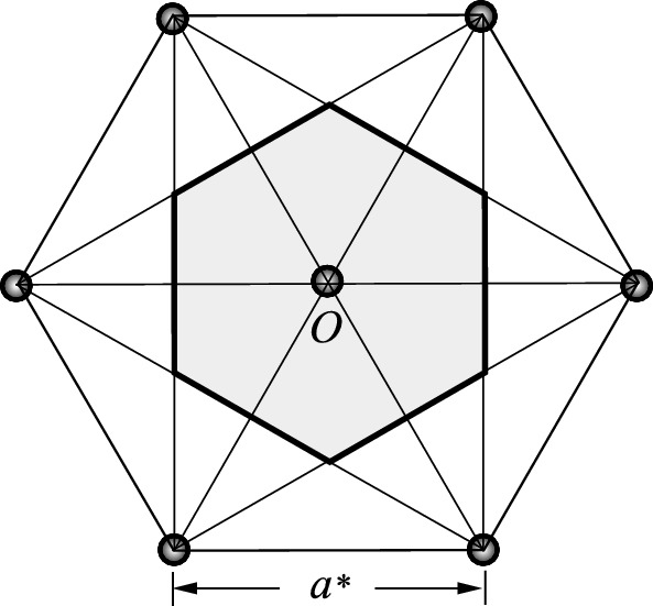
../images/325043_1_En_2_Chapter/325043_1_En_2_Fig50_HTML.png
Fig. 2.50

Construction of the first Brillouin zone for the plane simple hexagonal lattice. The reciprocal lattice points are shown at six corners and the origin

The 3D first Brillouin zone of the simple hexagonal lattice is obtained simply by introducing planes parallel to the c-axis through the sides of the hexagon and two planes perpendicular to the c-axis, each at distance c*/2 from O. The first Brillouin zone is therefore a hexagonal prism of height c* = 2π/c whose axis is parallel to the c-axis of the direct lattice. The hexagonal of side 4π/3a is oriented in the same direction as the hexagons of the direct lattice. It occupies a volume of $$ \left( {16\pi^{3} /\sqrt 3 } \right)/a^{2} c $$. The first Brillouin zone is shown in Fig. 2.51, together with some points of the reciprocal lattice.
../images/325043_1_En_2_Chapter/325043_1_En_2_Fig51_HTML.png
Fig. 2.51

First Brillouin zone for the simple hexagonal lattice. Some lattice points of the reciprocal lattice are also shown

Problems
  1. 1.

    Both AsH3 and SiCl4 are common gases for semiconductor growth and processing. Discuss their molecular bonding properties.

     
  2. 2.
    The ionic radii of Na, Cs, and Cl are 0.875 Å, 1.455 Å, and 1.475 Å, respectively.
    1. (a)

      For NaCl, the FCC structure is the preferred crystal structure. Verify that this structure prevents anion–anion or cation–cation contact.

       
    2. (b)

      Verify that the simple cubic structure has a higher atomic packing density than the FCC structure in CsCl crystals.


  3. 3.
    Calculate the atomic packing density for the following crystal structures:
    1. (a)

      Simple FCC

       
    2. (b)

      Simple hexagonal close-packed (HCP)

       
    3. (c)

      Diamond

       
    4. (d)

      Wurtzite.


  4. 4.

    Assume the cube containing a tetrahedron bond structure has a length a on each side. Calculate the bond length of the tetrahedron bond in terms of length a. Also, determine the angle between two tetrahedron bonds.

     
  5. 5.

    The primitive unit cell of a hexagonal close-packed (HCP) structure can be defined by unit vectors a and c. Prove that, using the incompressible spheres model, the ratio between c and a is $$ \sqrt {8/3} $$.

     
  6. 6.

    The primitive unit cell of a wurtzite structure can be defined by unit vectors a and c (Fig. 2.31). Derive the relations between a, c, and the bond length.

     
  7. 7.

    Prove that the reciprocal lattice of a simple hexagonal lattice is another simple hexagonal lattice. Determine the new lattice constants along the a-axis and c-axis.

     
  8. 8.
    1. (a)

      Derive the reciprocal lattice of the BCC structure. What is the new crystal structure?

       
    2. (b)

      What is the angle between G110 and G101?


  1. 9.

    Make a plot of the first two Brillouin zones of a primitive rectangular two-dimensional lattice with axes a, b = 2a.

     
  2. 10.

    Derive the dielectric constant tensor for a simple tetragonal crystal.

     
  3. 11.

    The hexagonal crystal is called an optically uniaxial crystal and has two principal dielectric constants: $$ \epsilon_{33} $$ along the c-axis and $$ \epsilon_{11} $$ in the basal plane. Show that the dielectric constant tensor of hexagonal crystals can be expressed as

     
$$ \epsilon = \left[ {\begin{array}{*{20}c} {\epsilon_{11} } & 0 & 0 \\ 0 & {\epsilon_{11} } & 0 \\ 0 & 0 & {\epsilon_{33} } \\ \end{array} } \right]. $$
Note: This can be done by considering a rotation of θ = π/3 about the c-axis. The new coordinates (x′ and y′) are related to the original coordinates through
$$ \left\{ {\begin{array}{*{20}c} {x^{\prime} = x\cos \theta + y\sin \theta } \\ {y^{\prime} = y\cos \theta - x\sin \theta } \\ \end{array} } \right.. $$