© Springer Nature Switzerland AG 2020
K. Y. ChengIII–V Compound Semiconductors and DevicesGraduate Texts in Physicshttps://doi.org/10.1007/978-3-030-51903-2_3

3. Electronic Band Structures of Solids

Keh Yung Cheng1, 2  
(1)
Department of Electrical and Computer Engineering, University of Illinois at Urbana-Champaign, Urbana, Illinois, USA
(2)
Department of Electrical Engineering, National Tsing Hua University, Hsinchu, Taiwan
 
 
Keh Yung Cheng

Abstract

The property that distinguishes semiconductors from other materials concerns the behavior of their charged carriers, in particular the existence of gaps in their electronic and photonic transition spectra. The microscopic behavior of charged carriers in a solid is most conveniently specified in terms of the electronic band structure. The metals are good conductors with overlapped conduction and valence bands, while insulators such as ionic crystals have large bandgaps of over 8 eV. The semiconductor crystals have a finite energy bandgap between metals and insulators. The purpose of this chapter is to develop the basic understanding of energy bandgap formation in solids. We start our discussion by first developing the free electron theory based on quantum theory in which the Fermi–Dirac statistics are used instead of the classical Boltzmann statistics. Then the spatial periodic potential of a solid is introduced according to Bloch’s theorem. Finally, the interference at Brillouin zone boundaries leads to constructive and/or destructive interferences of electron waves forming the energy bandgap.

3.1 Free Electron Theory and Density of States

The simplest model for describing electrons in solids is to assume that the valence electrons of an atom are free to move anywhere throughout the volume of the material. This is an appropriate model for a metallic solid. Of course, for an isolated atom, the electrons are confined by the large barrier of the Coulomb potential well and cannot move away from the nucleus. But when atoms bond together to form crystals, the potential barriers between atoms are lowered by the bonding energy. The simple model further assumes that the periodically arranged nuclei or the cores of the atoms are stationary and the core electrons shield the nuclear charge completely. Thus the potential appears qualitatively as shown in Fig. 3.1 where a constant electrostatic potential exists everywhere in the solid. Any potential ‘bump’ associated with individual atoms is smoothed out. This allows valence electrons to move freely within the crystal as free electrons. Therefore, we can use a ‘particle in a box’ approach to treat the problem. Furthermore, we neglect any electron–electron interactions by allowing only one free electron in the system.
../images/325043_1_En_3_Chapter/325043_1_En_3_Fig1_HTML.png
Fig. 3.1

Schematic of the potential within a perfectly periodic crystal lattice of positive cores. The vacuum level V0 is the energy that the electron must acquire in order to leave the crystal

3.1.1 One-Dimensional System
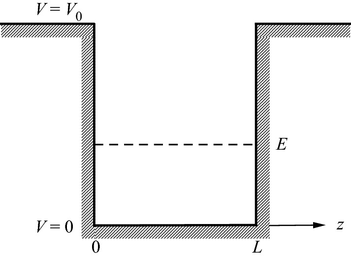
The simplified ‘one free electron theory’ in 1D can be pictured as a finite potential well with a well depth V0 and width L shown in Fig. 3.2. The only electron in the well has energy of E < V0. Since the barrier height of the well is finite, there are bound to be leakage waves outside the well. The 1D Schrödinger wave equation of this system outside the well is
../images/325043_1_En_3_Chapter/325043_1_En_3_Fig2_HTML.png
Fig. 3.2

Illustration of a finite square potential well experienced by an electron in the 1D free electron model

$$ - \frac{{\hbar^{2} }}{2m}\frac{{{\text{d}}^{2} \psi }}{{{\text{d}}z^{2} }} + V_{0} \psi = E\psi $$
(3.1)
Since E < V0, the solution of the wave function is
$$ \psi = A\exp \left( { - \alpha z} \right) + B\exp \left( {\alpha z} \right) $$
(3.2a)
and
$$ \alpha = \sqrt {2m\left( {V_{0} - E} \right)/\hbar^{2} } $$
(3.2b)
where V0E is the work function, and E is the kinetic energy of the electron. At z = ∞, ψ approaches 0, and B = 0. Thus, for z > L, the decay wave function outside the crystal is
$$ \psi \left( z \right) = A\exp \left( { - \alpha z} \right) $$
(3.3)
In GaAs, V0E ~ 4 eV and using the electron effective mass of 0.063m0, we have α ~ 2.57×107 cm−1. This means the amplitude of the wave function ψ(z) drops to 1/e in 3.89 Å or about a monolayer of atomic thickness. Therefore, under practical situations, we can neglect the penetration depth outside the crystal and use the infinite well approximation instead. The solution within the well becomes
$$ \psi \left( z \right) = \left\{ {\begin{array}{*{20}l} {A\sin \left( {k_{z} z} \right), } \hfill &amp; {0 \le z \le L} \hfill \\ {0,} \hfill &amp; {\text{elsewhere}} \hfill \\ \end{array} } \right. $$
(3.4)
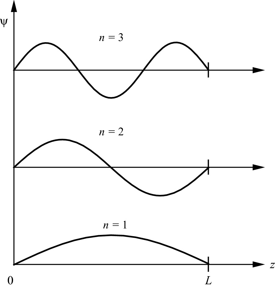
where the wave vector kz = /L and n = 1, 2, 3…. The first three wave functions are plotted in Fig. 3.3. Replacing the solutions (3.4) in the wave equation (3.1), we have
$$ - \frac{{\hbar^{2} }}{2m}\frac{{{\text{d}}^{2} }}{{{\text{d}}z^{2} }}\left[ {A\sin \left( {k_{z} z} \right)} \right] = \frac{{\hbar^{2} }}{2m}k_{z}^{2} \psi = E\psi $$
(3.5)
../images/325043_1_En_3_Chapter/325043_1_En_3_Fig3_HTML.png
Fig. 3.3

First three wave functions of a free electron in a square potential well of length L

The energy eigenvalue is related to the wave vector by
$$ E = \frac{{\hbar^{2} k_{z}^{2} }}{2m} $$
(3.6)
In the 1D free electron model, as shown in Fig. 3.4, the energy eigenvalue is a parabolic function of the wave vector kz.
../images/325043_1_En_3_Chapter/325043_1_En_3_Fig4_HTML.png
Fig. 3.4

Energy E plotted as a function of k according to (3.6)

3.1.2 Three-Dimensional System

  1. (a)

    Wave function ψ(x, y, z)

     
The general expression of the 3D wave function is
$$ - \frac{{\hbar^{2} }}{2m}\nabla^{2} \psi \left( {x,y,z} \right) + V_{0} \psi \left( {x,y,z} \right) = E\psi \left( {x,y,z} \right) $$
(3.7)
Using the infinite well approximation, we only have to consider ψ(x, y, z) inside the crystal (a cube of side L), where V = 0. Solving the wave equation by separation of variables, assuming ψ(x, y, z) = X(x) Y(y) Z(z), we get
$$ - \frac{{\hbar^{2} }}{2m}\left( {YZ\frac{{\partial^{2} X}}{{\partial x^{2} }} + XZ\frac{{\partial^{2} Y}}{{\partial y^{2} }} + XY\frac{{\partial^{2} Z}}{{\partial z^{2} }}} \right) = EXYZ $$
(3.8a)
or
$$ - \frac{{\hbar^{2} }}{2m}\left( {\frac{1}{X}\frac{{\partial^{2} X}}{{\partial x^{2} }} + \frac{1}{Y}\frac{{\partial^{2} Y}}{{\partial y^{2} }} + \frac{1}{Z}\frac{{\partial^{2} Z}}{{\partial z^{2} }}} \right) = E $$
(3.8b)
This equation is equivalent to three independent equations in X, Y, and Z. For example, the X-related equation is
$$ - \frac{{\hbar^{2} }}{2m}\frac{{\partial^{2} X}}{{\partial x^{2} }} = XE_{x} $$
(3.9)
where Ex is a constant. The solution of the wave equation in x is
$$ X = A_{x} { \sin }k_{x} x + B_{x} { \cos }k_{x} x $$
(3.10a)
and
$$ k_{x} = \sqrt {\frac{{2mE_{x} }}{{\hbar^{2} }}} $$
(3.10b)
Again, similar to the 1D system, we can use the condition of V0 = ∞ at x = 0 and x = L such that ψ(0) = ψ(L) = 0. Thus, Bx = 0 and
$$ X = A_{x} { \sin }k_{x} x $$
(3.11a)
and
$$ k_{x} = \frac{{n_{x} \pi }}{L} $$
(3.11b)
The wave functions of Y and Z can be solved in the same manner. We come to the final solution of the wave function in 3D as
$$ \psi \left( {x,y,z} \right) = A{ \sin }\left( {k_{x} x} \right){ \sin }\left( {k_{y} y} \right){ \sin }\left( {k_{z} z} \right) $$
(3.12a)
and
$$ k_{x} = \frac{{n_{x} \pi }}{L},  k_{y} = \frac{{n_{y} \pi }}{L},  k_{z} = \frac{{n_{z} \pi }}{L} $$
(3.12b)
where nx, ny, and nz are positive integers or quantum numbers which specify the relationship of ψ in the x-, y-, and z-directions. The amplitude A is calculated through the normalization process using $$ \mathop \smallint \limits_{\text{v}}^{{}} \psi^{*} \psi {\text{d}}x{\text{d}}y{\text{d}}z = 1 $$.
$$ A^{2} \mathop \int \limits_{0}^{L} \sin^{2} \left( {k_{x} x} \right){\text{d}}x\mathop \int \limits_{0}^{L} \sin^{2} \left( {k_{y} y} \right){\text{d}}y\mathop \int \limits_{0}^{L} \sin^{2} \left( {k_{z} z} \right){\text{d}}z = 1 $$
(3.13)
Since $$ \smallint \sin^{2} \left( {ax} \right){\text{d}}x = \frac{x}{2} - \frac{{\sin \left( {2ax} \right)}}{4a} $$, for a = ki = niπ/L,
$$ \left. {\frac{{\sin \left( {2ax} \right)}}{4a}} \right|_{0}^{L} = \frac{{\sin \left( {2n_{i} \pi } \right) - \sin 0^\circ }}{4a} = 0 $$
Therefore,
$$ \mathop \int \limits_{0}^{L} \sin^{2} \left( {k_{x} x} \right){\text{d}}x = \left. {\frac{x}{2}} \right|_{0}^{L} = \frac{L}{2} $$
(3.14a)
and
$$ A = \left( {2/L} \right)^{3/2} . $$
(3.14b)
The final solution of the wave function becomes
$$ \psi \left( {x,y,z} \right) = \left( {\frac{2}{L}} \right)^{3/2} \sin \left( {k_{x} x} \right)\sin \left( {k_{y} y} \right)\sin \left( {k_{z} z} \right) $$
(3.15a)
and
$$ k_{j} = \frac{{n_{i} \pi }}{L}\;{\text{for}} j = x, y, z \; {\text{and}} \;n_{i} = 1, 2, 3, \ldots $$
(3.15b)
  1. (b)

    Energy eigenvalues (E)

     
The allowed energy levels can be derived by inserting the wave function solution (3.15a) into the 3D wave function (3.7)
$$ - \frac{{\hbar^{2} }}{2m}\nabla^{2} \psi = E\psi \;{\text{and}}\;\nabla^{2} \psi = \frac{{\partial^{2} \psi }}{{\partial x^{2} }} + \frac{{\partial^{2} \psi }}{{\partial y^{2} }} + \frac{{\partial^{2} \psi }}{{\partial z^{2} }} $$
(3.16)
The second derivative terms in (3.16) are calculated using the wave function solution (3.15a) as follows:
$$ \frac{{\partial^{2} \psi }}{{\partial x^{2} }} = - \psi k_{x}^{2} ,  \frac{{\partial^{2} \psi }}{{\partial y^{2} }} = - \psi k_{y}^{2} ,  \frac{{\partial^{2} \psi }}{{\partial z^{2} }} = - \psi k_{z}^{2} $$
(3.17)
Then the wave equation becomes
$$ - \frac{{\hbar^{2} }}{2m}\left( {\frac{{\partial^{2} \psi }}{{\partial x^{2} }} + \frac{{\partial^{2} \psi }}{{\partial y^{2} }} + \frac{{\partial^{2} \psi }}{{\partial z^{2} }}} \right) = \frac{{\hbar^{2} }}{2m}\left( {k_{x}^{2} + k_{y}^{2} + k_{z}^{2} } \right)\psi = E\psi $$
(3.18)
which leads to the energy eigenvalues of
$$ E = \frac{{\hbar^{2} k^{2} }}{2m} = \frac{{\hbar^{2} }}{2m}\left( {k_{x}^{2} + k_{y}^{2} + k_{z}^{2} } \right) $$
(3.19)
Thus,
$$ E \propto k^{2} = k_{x}^{2} + k_{y}^{2} + k_{z}^{2} $$
(3.20)
In classical theory, the kinetic energy of a particle with momentum p can be expressed as
$$ K.E. = \frac{{p^{2} }}{2m} = \frac{1}{2m}\left( {p_{x}^{2} + p_{y}^{2} + p_{z}^{2} } \right) $$
(3.21)
Since our discussions of the total energy of the free electron involve kinetic energy only, the expressions of energy in (3.19) and (3.21) are identical. The allowed energy eigenvalues indicate that
$$ \varvec{p} = \hbar \varvec{k} $$
(3.22)

This is the de Broglie relationship, and p is the crystal momentum. However, it should be stressed that the wave vector k for electron wave functions in a periodic potential is not a measure of true physical momentum. As will be discussed later, the physically distinct values of the wave vector (crystal momentum) of an electron in a crystalline lattice—as opposed to those of a free particle, which can take any value—are restricted by the first Brillouin zone.

Further, the energy functions also contain the wave nature of the electron motion in the potential well. For n = 1 in (3.15b), k = π/L, and the allowed wavelength is λ = 2π/k = 2L or k = 2π/λ. The wavelength is related to the particle nature of the electron through
$$ \lambda = \frac{2\pi }{k} = \frac{2\pi \hbar }{{\sqrt {2mE} }} = \frac{h}{p} $$
(3.23)

Therefore, the electron with a momentum p will be diffracted like a wave with a wavelength λ in a crystal!

Since k = nπ/L, the energy eigenvalue can also be expressed as a function of n as
$$ E = \frac{{\hbar^{2} }}{2m}\left( {\frac{\pi }{L}} \right)^{2} n^{2} = \frac{{\hbar^{2} }}{2m}\left( {\frac{\pi }{L}} \right)^{2} \left( {n_{x}^{2} + n_{y}^{2} + n_{z}^{2} } \right) $$
(3.24)
or
$$ E \propto \left( {n_{x}^{2} + n_{y}^{2} + n_{z}^{2} } \right) = n^{2} $$
(3.25)

The results of (3.19) and (3.24) indicate that the 3D constant energy surface in n or k-space is a sphere. For each ki determined by ni there is a corresponding λi or mode. Each allowed energy state corresponding to a point ni can be displayed in the n-space with positive integer coordinates nx, ny, and nz. It is obvious that the energy eigenvalues are degenerate for nxnynz. For example, for (nx, ny, nz) equals (1, 2, 3), (1, 3, 2), (2, 3, 1), (2, 1, 3), (3, 1, 2), or (3, 2, 1), there are six degenerate energy states with the same energy. The number of degenerate states increases dramatically with increasing energy.

3.1.3 Density of States (DOS)

In many situations, such as when computing the electron distribution, it is necessary to know how the electrons are distributed in the energy spectrum. This could be done through the use of (3.24) to derive a density of states.
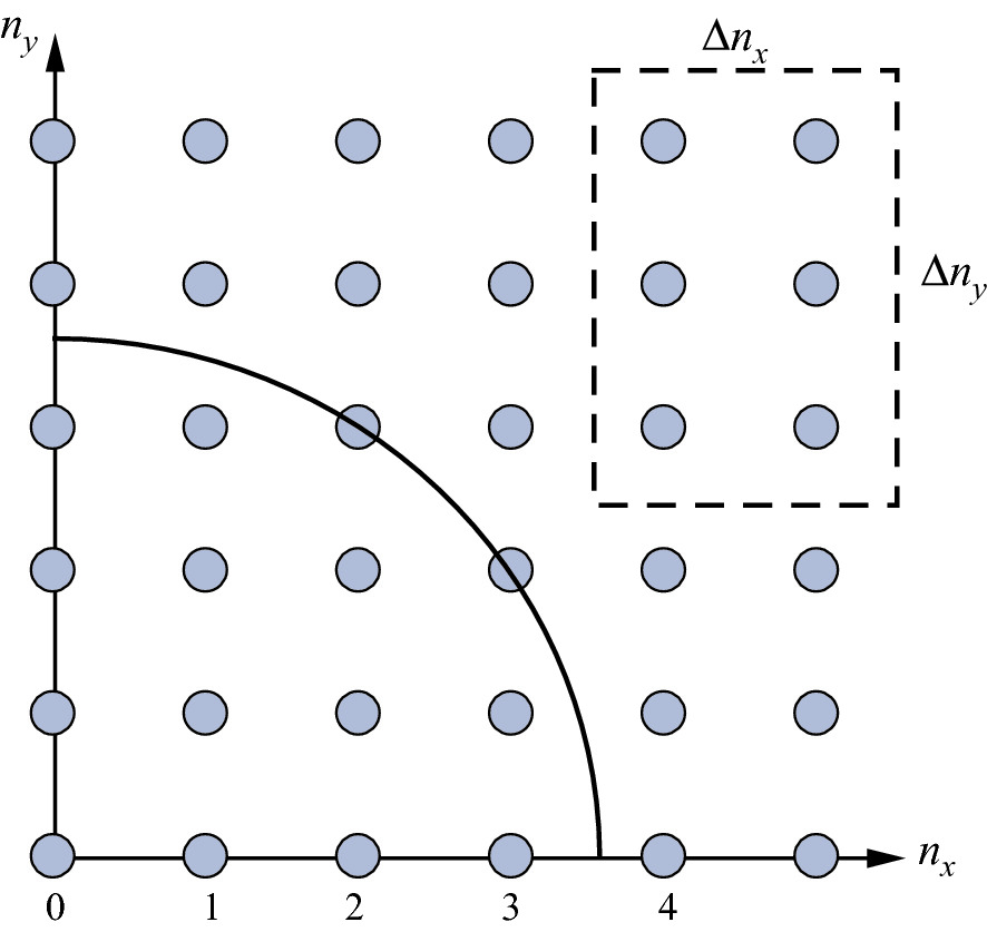
Consider a 2D crystal lattice in n-space where nz = 0, as shown in Fig. 3.5. Each lattice point is defined by a pair of (nx, ny). Since ki = niπ/L = 2π/λi, each point corresponds to a specific mode of wave oscillation. The number of normal modes of oscillation inside a finite area defined by a rectangular box is simply the number of lattice points within ΔnxΔny. In the 3D case, the number of normal modes of oscillation is ΔN′ ≡ ΔnxΔnyΔnz, which forms an orthorombic volume. In a crystal the spacing between these points is extremly close. For example, the wavelength of, say, a 3 eV electron is h/(2 mE)1/2 ≅ 7 Å and k = 2π/λ ≅ 9×107 cm−1. For a 1 cm3 cube, the number of oscillation modes in one coordinate direction is kL/π ~ 3 × 107! Therefore, we shall replace Δni by dn and ΔN′ ≈ dN′ = dnxdnydnz. Due to the large number of modes, they form a continuous band instead of discrete states.
../images/325043_1_En_3_Chapter/325043_1_En_3_Fig5_HTML.png
Fig. 3.5

Schematic of the states of an electron in a 2D infinte well. The circle corresponds to a constant energy

Since ni are all positive integers, as shown in Fig. 3.6, one need only count the ni in the first octant of the constant energy sphere. The number of normal modes in the first octant is
$$ N^{\prime} = \frac{1}{8}\left( {\frac{{4\pi n^{3} }}{3}} \right) $$
(3.26a)
where
$$ n = \frac{kL}{\pi } = \frac{L}{\pi }\sqrt {\frac{2mE}{{\hbar^{2} }}} $$
(3.26b)
../images/325043_1_En_3_Chapter/325043_1_En_3_Fig6_HTML.png
Fig. 3.6

Spherical surface corresponding to constant energies E and E + dE plotted in the momentum (n) space of a particle

Then, including the two possible spins into the total number, we have
$$ N = 2N^{\prime} = \frac{2}{8}\left( {\frac{4\pi }{3}} \right)\left( {\frac{2mE}{{\hbar^{2} }}} \right)^{3/2} \left( {\frac{L}{\pi }} \right)^{3} = \left( {\frac{1}{{3\pi^{2} }}} \right)L^{3} \left( {\frac{2mE}{{\hbar^{2} }}} \right)^{3/2} $$
(3.27)
The number of electron states within an energy interval dE, between E and E + dE, is
$$ {\text{d}}N = \left( {\frac{{{\text{d}}N}}{{{\text{d}}E}}} \right){\text{d}}E = \left( {\frac{{L^{3} }}{{2\pi^{2} }}} \right)\left( {\frac{2m}{{\hbar^{2} }}} \right)^{3/2} \sqrt E {\text{d}}E $$
(3.28)
The density of states (DOS) is defined as the number of states per unit energy interval near E per unit volume. It is expressed as
$$ D_{{3{\text{D}}}} \left( E \right) = \left( {\frac{{{\text{d}}N}}{{{\text{d}}E}}} \right)\frac{1}{{L^{3} }} = \frac{1}{{2\pi^{2} }}\left( {\frac{2m}{{\hbar^{2} }}} \right)^{3/2} \sqrt E\,      \left( {{\text{cm}}^{ - 3} {\text{eV}}^{ - 1} } \right) $$
(3.29)
In the 2D case, such as in a quantum well,
$$ N^{\prime} = \frac{{\pi n^{2} }}{4} = \frac{\pi }{4} \cdot \frac{{L^{2} }}{{\pi^{2} }} \cdot \frac{2mE}{{\hbar^{2} }} = \frac{N}{2} $$
(3.30)
Thus,
$$ \frac{{{\text{d}}N}}{{{\text{d}}E}} = \frac{{mL^{2} }}{{\pi \hbar^{2} }} $$
(3.31)
and
$$ D_{{2{\text{D}}}} \left( E \right) = \left( {\frac{{{\text{d}}N}}{{{\text{d}}E}}} \right)\frac{1}{{L^{2} }} = \frac{m}{{\pi \hbar^{2} }} = {\text{constant}}  \,\left( {{\text{cm}}^{ - 2} {\text{eV}}^{ - 1} } \right) $$
(3.32)
In the 1D case, such as in a quantum wire, N′ = n = kL/π.
$$ N = 2N^{\prime} = \frac{2L}{\pi }\sqrt {\frac{2mE}{{\hbar^{2} }}} $$
(3.33)
Then
$$ \frac{{{\text{d}}N}}{{{\text{d}}E}} = \frac{L}{\pi }\sqrt {\frac{2m}{{\hbar^{2} E}}} $$
(3.34)
and
$$ D_{{ 1 {\text{D}}}} \left( E \right) = \left( {\frac{{{\text{d}}N}}{{{\text{d}}E}}} \right)\frac{1}{L} = \frac{1}{\pi \hbar }\sqrt {\frac{2m}{E}} \propto \frac{1}{\sqrt E }\,\left( {{\text{cm}}^{ - 1} {\text{eV}}^{ - 1} } \right) $$
(3.35)
Finally, when the volume of the 3D confinement of a potential well reduces to contain only one energy state, the structure becomes a quantum dot. Since there are two electrons allowed per state E0, one spin-up and one spin-down, the DOS of zero-dimension (0D) is given as
$$ D_{{0{\text{D}}}} \left( E \right) = 2\delta \left( {E - E_{0} } \right) $$
(3.36)
The delta function indicates that only when E = E0 is there a state. The DOS as a function of energy for 3D, 2D, 1D, and 0D distributions is plotted in Fig. 3.7.
../images/325043_1_En_3_Chapter/325043_1_En_3_Fig7_HTML.png
Fig. 3.7

Density of states distributions in bulk (3D), quantum well (2D), quantum wire (1D), and quantum dot (0D) structures

3.2 Periodic Crystal Structure and Bloch’s Theorem

The simple model of the free electron theory using one-electron approximation of a square potential well has been successful in accounting for some physical properties of solids, in particular those of metals. However, in crystals, the ‘free’ electron situation is not very accurate. Therefore, this overly simplified model needs refinements in order to improve its ability to explain the properties of semiconductors. One obvious addition to the model is to add the spatial dependence of the potential experienced by a valence electron in a crystal. The effect of the added potential associated with the ion cores is particularly pronounced in periodic ion-core potentials. However, this also imposes a concomitant constraint on the wave functions that describing the motion of an electron in the periodic potential. Fortunately, this added constraint can be treated easily using the theory that Felix Bloch proposed in 1928.

3.2.1 Bloch’s Theorem

The free electron theory developed so far has used the square well approximation that leads to the sinusoidal wave function solutions of (3.15a). In our present assumption, to simplify the discussions, all deviations from a perfect periodicity will be neglected. This means that even the surface effects are removed by assuming an infinitely extended potential. For an infinite 1D system with a uniform potential energy of V (=constant), the wave function is now represented by a traveling plane wave of the form
$$ \psi_{k} \left( z \right) = A\exp \left( {ikz} \right) $$
(3.37)

This leads to a uniform distribution function of $$ \psi_{k}^{*} \psi_{k} = \psi_{k}^{2} = A^{2} $$ = constant. Therefore, the system is translationally invariant.

Now a periodic potential energy is introduced to the system. This potential is the sum of the electrostatic potential due to ion cores of lattice atoms and the potential due to all other outer electrons. The charge density from outer electrons would have the same average value in every unit cell of the crystal and would also be periodic. Thus the total potential has the periodicity of the lattice. Based on this reasoning, Bloch argued that the total potential energy V(z) with a periodicity of the lattice could be substituted into the 1D Schrödinger equation.
$$ - \frac{{\hbar^{2} }}{2m}\frac{{{\text{d}}^{2} \psi }}{{{\text{d}}z^{2} }} + V\left( z \right)\psi = E\psi $$
(3.38)
He concluded that the wave functions, which satisfy (3.38), subject to such a periodic potential, must be of the form
$$ \psi_{k} \left( z \right) = u_{k} \left( z \right)\exp \left( {ikz} \right) $$
(3.39)
where uk(z) are functions with the same periodicity of the lattice. The theory leading to (3.39) is known as Bloch’s theorem, and functions uk(z) are called Bloch functions.
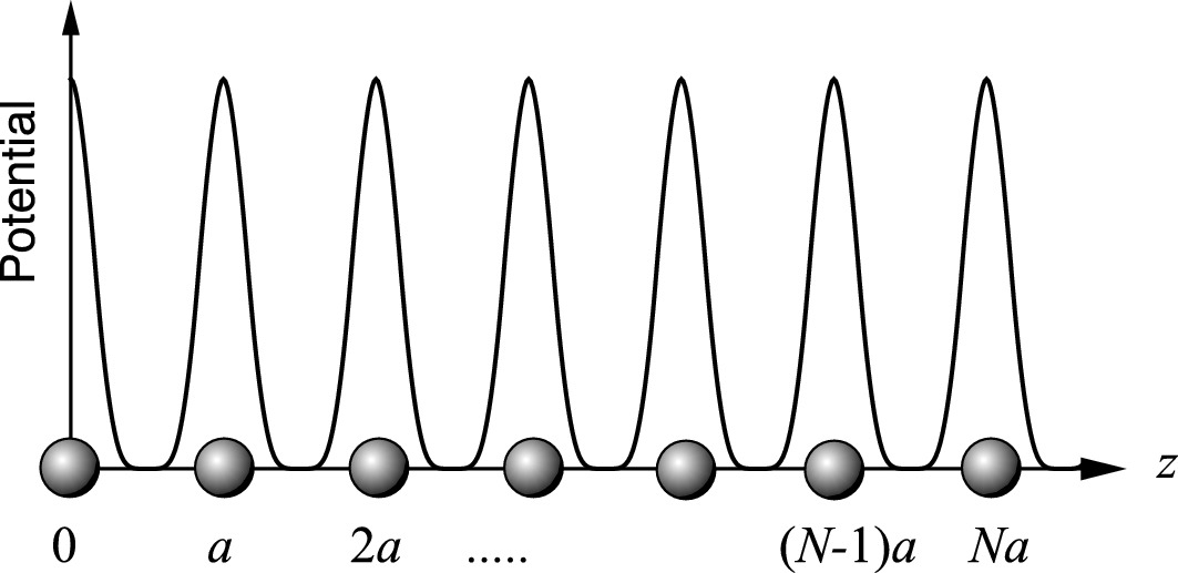
To discuss Bloch’s theorem, let us first examine a 1D crystal, shown in Fig. 3.8, which has a linear array of atoms with interatomic (lattice) spacing a. Since the potential has the periodicity of the lattice, then
$$ V\left( z \right) = V\left( {z + a} \right) $$
(3.40)
for any value of z. For such a periodic potential system, the wave function solutions shall repeat after N unit cell length, where N is an arbitrary number. Then
$$ \psi \left( z \right) = \psi \left( {z + Na} \right) $$
(3.41)
for any value of z. In view of the translational symmetry of the system, the wave functions of the neighboring unit cells can be related by an expression of the form
$$ \psi \left( {z + a} \right) = \lambda \psi \left( z \right) $$
(3.42)
where λ is a function to be determined. This means that for the location separated by N unit cells,
$$ \psi \left( {z + Na} \right) = \lambda^{N} \psi \left( z \right) = \psi \left( z \right) $$
(3.43)
Comparing (3.41) and (3.43) shows that λN = 1 and λ must be one of the N roots of unity:
$$ \lambda = \exp \left( {i2\pi P/N} \right) $$
(3.44)
where P is an integer representing the number of complete cycles in the distance Na. Therefore, we can relate the wave vector k to P by k = 2πP/Na. Then, for ψ(z + a),
$$ \lambda = \exp \left( {ika} \right) $$
(3.45)
../images/325043_1_En_3_Chapter/325043_1_En_3_Fig8_HTML.png
Fig. 3.8

Periodic potential for a linear atomic lattice. We may assume that the wave functions of all eigenstates must repeat after some arbitrary number N of unit cells

Thus, one form of the wave function is
$$ \psi \left( {z + a} \right) = \exp \left( {ika} \right)\psi \left( z \right) $$
(3.46)
An equivalent and general form of the above equation is that the wave function is the modulated plane wave
$$ \psi \left( z \right) = \exp \left( {ikz} \right)u_{k} \left( z \right) $$
(3.47)
where uk(z) is a periodic function which also has the translational periodicity of the lattice. This is the one-dimensional Bloch function.
It is clear from (3.42), (3.45), and (3.47) that
$$ \begin{aligned} u_{k} \left( {z + a} \right) &amp; = \exp \left[ { - ik\left( {z + a} \right)} \right]\psi \left( {z + a} \right) \\ &amp; = \exp \left[ { - ik\left( {z + a} \right)} \right]\lambda \psi \left( z \right) \\ &amp; = \exp \left[ { - ik\left( {z + a} \right)} \right]\exp \left( {ika} \right)\psi \left( z \right) \\ &amp; = \exp \left( { - ikz} \right)\psi \left( z \right) = u_{k} \left( z \right) \\ \end{aligned} $$
(3.48)

The function uk(z) is thus periodic with a period a.

We can expand this 1D result to 3D crystal systems with a periodic potential function proportional to the periodicity of the lattice, shown as
$$ V\left( \varvec{r} \right) = V\left( {\varvec{r} + \varvec{T}} \right)\;{\text{and}}\;\varvec{T} = n_{1} \varvec{a} + n_{2} \varvec{b} + n_{3} \varvec{c} $$
(3.49)
The wave functions which satisfy the corresponding Schrödinger wave equation have the form of a plane wave with a propagation constant k modulated by a function uk(r) whose periodicity is that of the crystal lattice.
$$ \left\{ {\begin{array}{*{20}l} {\psi_{k} \left( \varvec{r} \right) = u_{k} \left( \varvec{r} \right)\exp \left( {i\varvec{k} \cdot \varvec{r}} \right)} \hfill \\ {u_{k} \left( \varvec{r} \right) = u_{k} \left( {\varvec{r} + \varvec{T}} \right)} \hfill \\ \end{array} } \right. $$
(3.50)

3.2.2 Reduced Zone Representation

The 1D Bloch function of (3.39) can be written as
$$ \psi \left( z \right) = u_{k} \left( z \right)\exp \left( {i2\pi Pz/Na} \right) $$
(3.51)

In this equation, as will become clear next, it is not necessary to use the value for P which is larger than ±(N/2), corresponding with k = ±(π/a). Any excess periodicity can be transferred into the uk(z) factor of the Bloch function. We notice that the range of wave vector from k = –(π/a) to k = +(π/a) corresponds to the first Brillouin zone in reciprocal lattice of the 1D lattice with a lattice spacing of a. Thus it is useful to examine the Bloch wave function near the origin of the k-space.

For the 3D case, the Bloch wave function whose wave vectors differ from ψk(r) by a reciprocal lattice vector G according to
$$ \varvec{k} + \varvec{G} = {\varvec{k}^{\prime}} $$
(3.52)
is also equivalent in terms of the electron energy. It shows
$$ \begin{aligned} \psi_{{k + {\text{G}}}} \left( \varvec{r} \right) &amp; = u_{{k + {\text{G}}}} \left( \varvec{r} \right)\exp \left[ {i\left( {\varvec{k} + \varvec{G}} \right) \cdot \varvec{r}} \right] \\ &amp; = \left[ {u_{{k + {\text{G}}}} \left( \varvec{r} \right)\exp \left( {i\varvec{G} \cdot \varvec{r}} \right)} \right]\exp \left( {i\varvec{k} \cdot \varvec{r}} \right) \\ &amp; = u_{k} \left( \varvec{r} \right)\exp \left( {i\varvec{k} \cdot \varvec{r}} \right) \\ \end{aligned} $$
Thus,
$$ \psi_{{k + {\text{G}}}} \left( \varvec{r} \right) = \psi_{k} \left( \varvec{r} \right) $$
(3.53)

Here, we used $$ u_{{k + {\text{G}}}} \left( \varvec{r} \right) = u_{k} \left( \varvec{r} \right) $$ and $$ \exp \left( {i\varvec{G} \cdot \varvec{r}} \right) = \exp \left( {i2m\pi } \right) = 1 $$.

The Schrödinger wave equations for ψk and ψk+G can be expressed, respectively, as
$$ H\psi_{k} = E_{k} \psi_{k} $$
(3.54)
and
$$ H\psi_{{k + {\text{G}}}} = E_{{k + {\text{G}}}} \psi_{{k + {\text{G}}}} $$
(3.55)
Using (3.53), we can combine these wave equations into
$$ E_{k} \psi_{k} = E_{{k + {\text{G}}}} \psi_{{k + {\text{G}}}} $$
(3.56)
or
$$ E_{k} = E_{{k + {\text{G}}}} $$
(3.57)
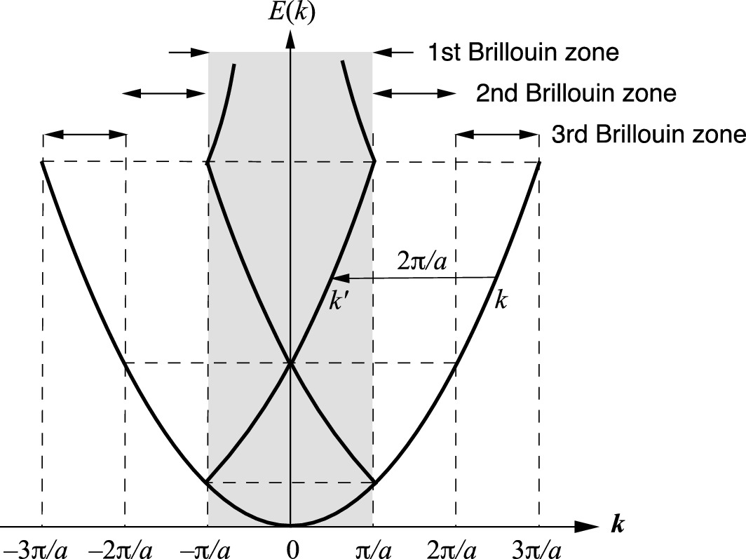
Thus, the translational real-space periodicity of the lattice potential imposes periodicity on the energy eigenvalues and wave functions in reciprocal k-space. To examine the energy–momentum relationships of the electron, one needs only know these functions for k- values in the first Brillouin zone, k′. For example, as shown in Fig. 3.9, assume π/ak ≤ 3π/a in a 1D system with a lattice constant a, or
../images/325043_1_En_3_Chapter/325043_1_En_3_Fig9_HTML.png
Fig. 3.9

Energy as a function of wave vector for electrons in a one-dimensional crystal of lattice constant a, where the amplitude of the periodic potential is set to zero. The continuous energy function is shown as a multiple-valued function of k in the shaded first Brillouin zone using the reduced zone representation

$$ k = \frac{2\pi }{a} + k^{\prime}\;{\text{and}}\; - \frac{\pi }{a} &lt; k^{\prime} &lt; \frac{\pi }{a} $$
(3.58)
Then,
$$ \begin{aligned} \psi_{k} \left( z \right) &amp; = u_{k} \left( z \right)\exp \left( {ikz} \right) \\ &amp; = \left\{ {u_{k} \left( z \right)\exp \left[ {i\left( {2\pi /a} \right)z} \right]} \right\}\exp \left( {ik^\prime z} \right) \\ \end{aligned} $$
(3.59)
where exp[i(2π/a)z] is a periodic function with the same periodicity as uk(z). We can rewrite the term inside the curly bracket as a new periodic function $$ u_{{k^{\prime}}} \left( z \right) $$ with the same periodicity. Thus,
$$ \psi_{k} \left( z \right) = u_{k^\prime} \left( z \right)\exp \left( {ik^\prime z} \right) . $$
(3.60)

This reduces the Bloch wave number to the range –π/ak ≤ π/a, which is the first Brillouin zone. Other higher-order wave vectors can also be reduced to the first Brillouin zone using the reduced zone representation.

3.2.3 Empty Lattice Model—Energy Band Calculation for an FCC Crystal

In the free electron model, it is simple to discuss electron energy and wave vector without regard for the crystallography of the solid. As soon as we take the periodic potential into consideration, the Brillouin zone boundaries (surfaces) in k-space become particularly important. Therefore, the following discussion of the relationship between energy and momentum for electrons in crystals will be in k-space.

For the free electron model, the allowed energy values are distributed continuously in a parabolic form of
$$ E = \frac{{\hbar^{2} k^{2} }}{2m} $$
(3.19)
When a finite periodic potential distribution is added, the periodic lattice information needs to be incorporated. Since we consider one electron in the crystal lattice only, without including electron–electron wave interactions, this approach is also called the empty lattice model. The 3D parabolic E-k relationship is modified with the incorporation of the reciprocal lattice vector G as
$$ E = \frac{{\hbar^{2} }}{2m}\left| {\varvec{k} + \varvec{G}} \right|^{2} $$
(3.61)
where k = kxa + kyb + kzc and G = ha* + kb* + lc*. As we have discussed in Sect. 2.​5, G contains the lattice information for a specific crystal structure. For FCC crystals, using the translation vectors of the G-vector from (2.​65) leads to
$$ \begin{aligned} E_{\text{FCC}} &amp; = \frac{{\hbar^{2} }}{2m}\left\{ {\left[ {k_{x} + \frac{2\pi }{a}\left( { - h + k + l} \right)} \right]^{2} } \right. + \left[ {k_{y} + \frac{2\pi }{a}\left( {h - k + l} \right)} \right]^{2} \\ &amp; \quad \quad \quad \quad \left. { + \left[ {k_{z} + \frac{2\pi }{a}\left( {h + k - l} \right)} \right]^{2} } \right\} \\ \end{aligned} $$
(3.62)
By properly adjusting the system of units used, the expression can be reduced to
$$ E = \left( {k_{x} + G_{x} } \right)^{2} + \left( {k_{y} + G_{y} } \right)^{2} + \left( {k_{z} + G_{z} } \right)^{2} $$
(3.63)
where Gx, Gy, and Gz are integers to be selected for different energy states. Based on this equation, we can calculate the E-k curves, or the electronic band structure, along the $$ \left\langle {100} \right\rangle $$ and $$ \left\langle {111} \right\rangle $$ axes in the reduced zone representation.
  1. (a)

    $$ \left\langle {100} \right\rangle $$

     
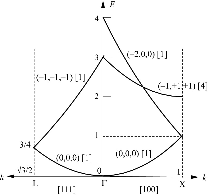
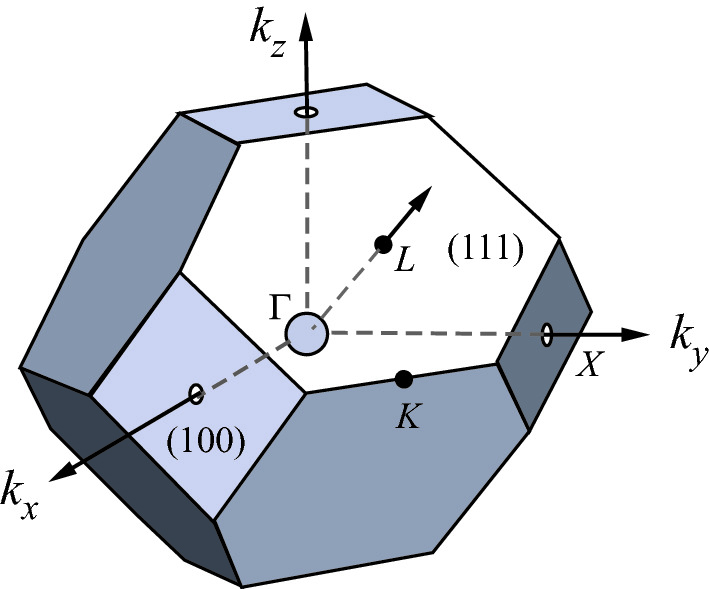
As shown in Fig. 3.10, along [100], ky = kz = 0, and $$ E = \left( {k_{x} + G_{x} } \right)^{2} + G_{y}^{2} + G_{z}^{2} $$. The lowest energy state is located at Gx = Gy = Gz = 0 and $$ E = k_{x}^{2} $$. The E-k curve follows a parabola and E = 1 at kx = 1. Figure 3.11 shows the lowest three E-k curves along [100].
../images/325043_1_En_3_Chapter/325043_1_En_3_Fig10_HTML.png
Fig. 3.10

Brillouin zone of the face-centered cubic lattice. The high symmetry points Γ, L, X, and K correspond to the zone center, $$ \left\langle {111} \right\rangle $$, $$ \left\langle {100} \right\rangle $$, and $$ \left\langle {110} \right\rangle $$ directions, respectively

../images/325043_1_En_3_Chapter/325043_1_En_3_Fig11_HTML.png
Fig. 3.11

Band structure for a free electron in an FCC lattice along [100] and [111] in the first Brillouin zone. For each curve, the selected G’s and degeneracy (in brackets) are indicated

To continue, using the reduced zone scheme, the next E needs to start at E = 1 (kx = 1) and increase as kx approaches zero. By trial and error, there are two possible G’s that match this condition. However, G(−1, −1, 0) is not selected due to the lack of continuation in the third Brillouin zone and other diffraction directions. The appropriate G’s are (Gx, Gy, Gz) = (–2, 0, 0), and E = (kx – 2)2. Started from kx = 1, E = 1, the E-k curve increases toward kx = 0, E = 4.

The next higher energy level is E = 3 at kx = 0. This energy level matches the second lowest energy state along [111] shown next. This can be calculated by setting (Gx, Gy, Gz) = (–1, ±1, ±1), which has a four-fold degeneracy. The E-k dispersion relationship is E = (kx – 1)2 + 2. At kx = 1, E = 2, and at kx = 0, E = 3.

  1. (b)

    $$ \left\langle {111} \right\rangle $$

     
In the reciprocal lattice of FCC structures, assuming the first Brillouin zone boundary along 〈100〉, measured from the zone center Γ, has a length of kmax = 1. From the geometry of the Wigner–Seitz cell shown in Fig. 3.10, the Brillouin zone boundary along 〈111〉 has a length of ($$ \sqrt 3 /2 $$) kmax and kx = ky = kz. The lowest energy is at (Gx, Gy, Gz) = (0,0,0). $$ E = k_{x}^{2} + k_{y}^{2} + k_{z}^{2} = k^{2} $$. At k = 0, E = 0, and at $$ k = \left( {\sqrt 3 /2} \right)k_{ \hbox{max} } $$, E = 3/4.
The next energy level should have an energy of 3/4 at $$ \left( {\sqrt 3 /2} \right)k_{ {max} } $$. This corresponds to a set of (Gx, Gy, Gz) = (–1, –1, –1). Then
$$ \begin{aligned} E &amp; = \left( {k_{x} - 1} \right)^{2} + \left( {k_{y} - 1} \right)^{2} + \left( {k_{z} - 1} \right)^{2} \\ &amp; = \left( {k_{x}^{2} + k_{y}^{2} + k_{z}^{2} } \right) - 2\left( {k_{x} + k_{y} + k_{z} } \right) + 3 \\ &amp; = k^{2} - 2\sqrt 3 k + 3 \\ \end{aligned} $$
(3.64)
where we recognized that
$$ \begin{aligned} \left( {k_{x} + k_{y} + k_{z} } \right)^{2} &amp; = \left( {k_{x}^{2} + k_{y}^{2} + k_{z}^{2} } \right) \\ &amp; \quad + 2\left( {k_{x} k_{y} + k_{y} k_{z} + k_{z} k_{x} } \right) = 3k^{2} \\ \end{aligned} $$
and
$$ k_{x} + k_{y} + k_{z} = \sqrt 3 k $$
(3.65)
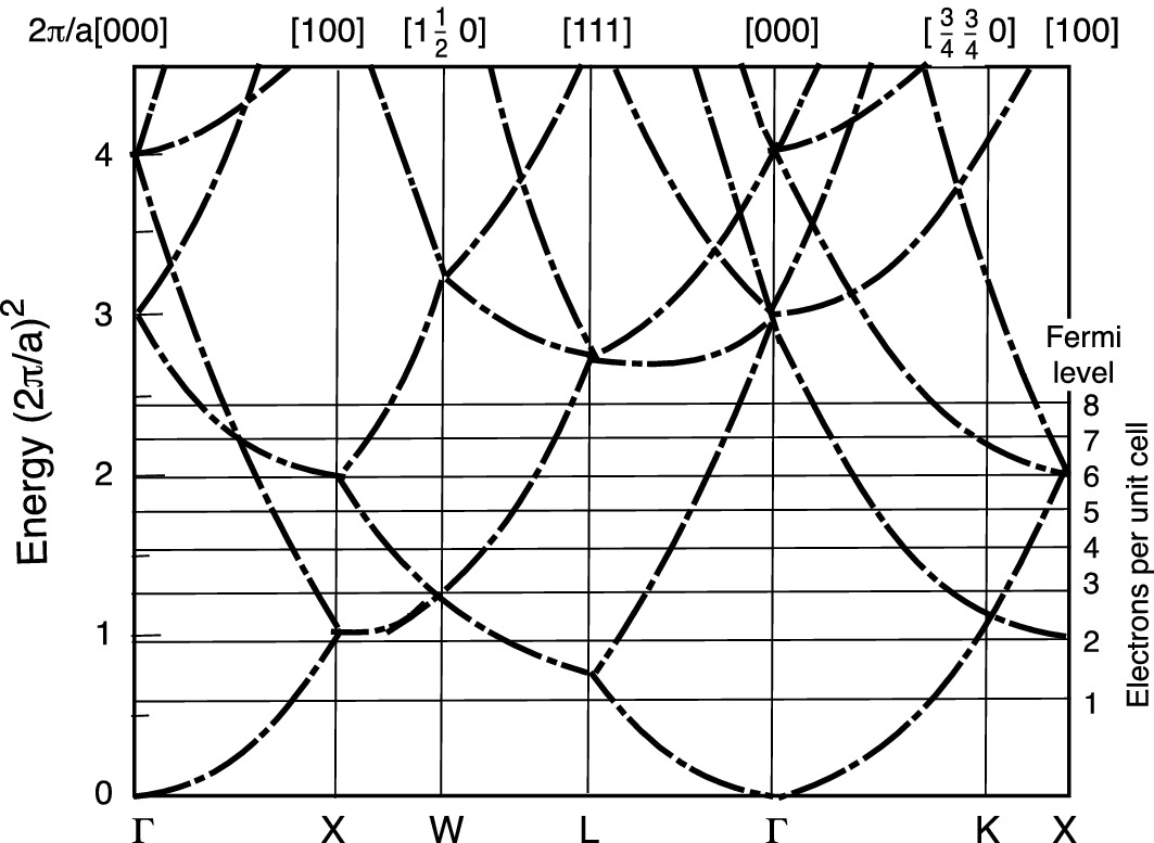
According to (3.64), at k = 0, E = 3, and at k = 0.868 kmax, E = 3/4. This E-k curve is also shown in Fig. 3.11. One can continue the process along [110] and other major directions of the FCC crystal to complete the E-k diagram shown in Fig. 3.12.
../images/325043_1_En_3_Chapter/325043_1_En_3_Fig12_HTML.png
Fig. 3.12

Band structure for a free electron in an FCC lattice in the first Brillouin zone.

Reprinted with permission from [1], copyright Wiley

In the free electron theory, where the potential induced by the core ions is neglected, the energy band is a continuous parabola. However, the above results indicate that the motion of electrons is not free, but is constrained by the spatial arrangement of the periodic potential associated with the lattices. Nevertheless, in this simple ‘one’ electron model, it allows the Bloch function wave of all energies to extend without attenuation through a crystal.

3.3 Nearly Free Electron Approximation and the Energy Gap

3.3.1 Origin of Bandgaps
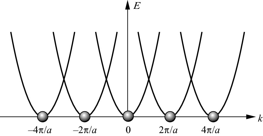
The E-k dispersion curve of ‘one’ free electron in a 1D system with a small periodic potential function, equivalent to the lattice constant of semiconductors, can be represented by a parabolic curve centered on a reciprocal lattice point. The possible electron states are not restricted to that single parabola in k-space, but are equally as likely to be found on a parabola shifted by any G-vector as shown in Fig. 3.13. This is due to the periodic property of E, i.e.,
../images/325043_1_En_3_Chapter/325043_1_En_3_Fig13_HTML.png
Fig. 3.13

Energy bands for an electron in a 1D periodic array of potential with a periodicity of a plotted in the repeated-zone scheme

$$ E\left( \varvec{k} \right) = E\left( {\varvec{k} + \varvec{G}} \right) = \left( {\hbar^{2} /2m} \right)\left| {\varvec{k} + \varvec{G}} \right|^{2} $$
(3.66)

However, when there is only one electron in the system, the electron–electron wave interactions are missing, and the resulting energy band structure shows only the crystal structural property, e.g., as illustrated in Fig. 3.12 for FCC lattices. Of course, in reality, there are extremely large quantities of electrons available in semiconductors. To improve the model, we shall allow more electrons in the crystal lattice such that the electron–electron wave interactions could be included.

When an electron wave propagates through the crystal lattice, it gets scattered in all directions from the lattice atoms. Because of the periodic nature of the lattice, in certain directions, waves scattered by many lattice points interfere constructively and a strong scattered beam results. For example, the Bragg condition for an incident wave normal to the crystal plane with a lattice periodicity of a is = 2a or k = /a. The wave vector that fulfills the Bragg condition simply equals one half of the reciprocal lattice vector G, i.e., k = ± G/2. In general, since the scattering from the lattice involves all wave numbers, a plane wave of wave number k and energy E(k) will mix with other electron waves with wave number k + Gn for all n’s. The mixing becomes strong only when the electron waves propagating through the crystal lattice are of equal energy where E(k) = E(k ± G) or |k| = |k ± G| or k = ± Gn/2. Again, the Bragg condition for strong reflection occurs at k = ± Gn/2. Therefore, the backscattering becomes very strong, and the electron is unable to propagate through. The forward and back reflected waves establish a standing wave in the crystal. Assuming the contributions from the nearest neighboring waves dominate the resulting waves, the contribution from other reciprocal lattice vectors can be neglected.

The wave functions at the edge of the first Brillouin zone at ± G/2 = ±π/a are
$$ \psi \left( { + \pi /a} \right) = A\exp \left( {ik \cdot r} \right) = A\exp \left( {iGz/2} \right) $$
(3.67a)
and
$$ \psi \left( { - \pi /a} \right) = A\exp \left[ {i\left( {G/2 - G} \right)z} \right] = A\exp \left( { - iGz/2} \right) $$
(3.67b)
The resultant forward (ψ+) and reflected (ψ) plane waves are
$$ \left\{ {\begin{array}{*{20}c} {\psi_{ + } \sim \exp \left( {iGz/2} \right) + \exp \left( { - iGz/2} \right)\sim \cos \left( {\pi z/a} \right)} \\ {\psi_{ - } \sim \exp \left( {iGz/2} \right) - \exp \left( { - iGz/2} \right)\sim \sin \left( {\pi z/a} \right)} \\ \end{array} } \right. $$
(3.68)
The corresponding electron probability densities are
$$ \left\{ {\begin{array}{*{20}c} {\rho_{ + } = \psi_{ + }^{*} \psi_{ + } \sim \cos^{2} \left( {\pi z/a} \right)} \\ {\rho_{ - } = \psi_{ - }^{*} \psi_{ - } \sim \sin^{2} \left( {\pi z/a} \right)} \\ \end{array} } \right. $$
(3.69)
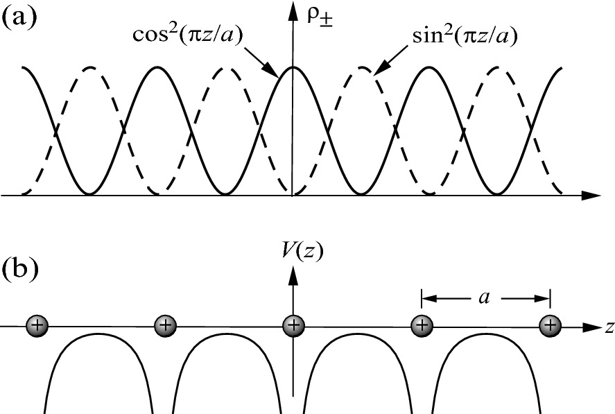
As illustrated in Fig. 3.14, the probability density of ψ+ (solid curve) peaks at the valleys of the potential energy function, and the associated electrons spend more time at the lower potential region. Thus, electrons associated with ψ+ have a lower total energy. The peaks of the probability density of ψ (dashed curve) correspond to the peaks of the potential energy function and have a higher total energy. The degeneracy of the two states, ψ+ and ψ, with different energies at certain wave numbers, breaks the continuity of the parabolic E-k dispersion curve and forms the energy gap (Fig. 3.15). At k = ± nπ/a, the wave functions of the upper and lower boundaries of the energy gap are ψ and ψ+, respectively. There is no allowed energy value in between ψ+ and ψ at the zone boundary, and an energy bandgap exists in this forbidden region.
../images/325043_1_En_3_Chapter/325043_1_En_3_Fig14_HTML.png
Fig. 3.14

Schematic illustration of the relationship between a electron charge density distribution and b the ion core positions in a 1D lattice

../images/325043_1_En_3_Chapter/325043_1_En_3_Fig15_HTML.png
Fig. 3.15

Electronic band structure for a 1D crystal with periodicity a in the nearly free electron approximation. Many electrons are presented. The dashed curve shows the continuous E-k curve of the free electron model

3.3.2 Energy Gap—A Quantitative Approach

The behavior of the energy bands in the vicinity of the bandgaps can be analyzed by considering the Schrödinger equation for a translational periodic potential energy expressed in terms of Fourier expansion. In a 1D lattice similar to that shown in Fig. 3.14b, the periodic potential with a periodicity a is expressed as V(z) = V(z + a). The Fourier transformation of the symmetric periodic function is
$$ V\left( z \right) = \mathop \sum \limits_{n} V_{n} \exp \left( {i2n\pi z/a} \right) $$
(3.70)
Since V(z) is an even function, by neglecting the sine term, V(z) becomes
$$ \begin{aligned} V\left( z \right) &amp; \cong V_{0} + \mathop \sum \limits_{n} \left[ {2V_{n} \left( z \right)\cos \left( {2n\pi z/a} \right)} \right] \\ &amp; = V_{0} + V_{1}^{'} \left( z \right) + V_{2}^{'} \left( z \right) + \cdots \\ \end{aligned} $$
(3.71)
Further neglecting higher-order terms, the lattice potential function can be represented as
$$ V\left( z \right) \approx V_{0} + V_{1}^{\prime } \left( z \right) $$
(3.72)
and
$$ \begin{aligned} V_{1}^{'} \left( z \right) &amp; = 2V_{1} \cos \left( {2\pi z/a} \right) \\ &amp; = V_{1} \left[ {\exp \left( {i2\pi z/a} \right) + \exp \left( { - i2\pi z/a} \right)} \right] \\ \end{aligned} $$
(3.73)
where V1 is a constant.
The wave functions of this lattice structure can be expressed as ψ(z) = u(z)exp(ikz). Due to Bragg diffraction at zone boundaries, the incident and reflected waves form constructive interference. At the first Brillouin zone boundary, k = ± π/a, the wave functions are
$$ \begin{aligned} \psi \left( z \right) &amp; = A_{1} \exp \left( {ikz} \right) + A_{2} \exp \left( { - ikz} \right) \\ &amp; = A_{1} \exp \left( {i\pi z/a} \right) + A_{2} \exp \left( { - i\pi z/a} \right) \\ \end{aligned} $$
(3.74)
where A1 and A2 are constants, and
$$ \frac{{\partial^{2} \psi \left( z \right)}}{{\partial z^{2} }} = - k^{2} \psi \left( z \right) $$
(3.75)
Replacing (3.72) and (3.75) in the Schrödinger wave equation
$$ \frac{{\hbar^{2} }}{2m}\frac{{\partial^{2} \psi }}{{\partial z^{2} }} + \left[ {E - V\left( z \right)} \right]\psi = 0 $$
(3.76)
it becomes
$$ - \frac{{\hbar^{2} k^{2} }}{2m}\psi \left( z \right) + \left[ {E - V_{0} - V_{1}^{\prime } \left( z \right)} \right]\psi \left( z \right) = 0 $$
(3.77)
Letting $$ E_{k} \equiv \displaystyle{\frac{{\hbar^{2} k^{2} }}{2m}} $$ and using $$ \psi \left( z \right) = A_{1} \exp \left( {ikz} \right) + A_{2} \exp \left( { - ikz} \right) $$, the wave equation becomes
$$ \begin{aligned} &amp; \left( {E - E_{k} } \right)\left[ {A_{1} \exp \left( {ikz} \right) + A_{2} \exp \left( { - ikz} \right)} \right] \\ &amp; = \left[ {V_{0} + V_{1}^{'} \left( z \right)} \right]\left[ {A_{1} \exp \left( {ikz} \right) + A_{2} \exp \left( { - ikz} \right)} \right] \\ \end{aligned} $$
(3.78)
Regrouping, we have
$$ \begin{aligned} &amp; \left( {E - E_{k} - V_{0} } \right)\left[ {A_{1} \exp \left( {ikz} \right) + A_{2} \exp \left( { - ikz} \right)} \right] \\ &amp; = \left\{ {V_{1} \left[ {\exp \left( {i2kz} \right) + \exp \left( { - i2kz} \right)} \right]} \right\}\left[ {A_{1} \exp \left( {ikz} \right) + A_{2} \exp \left( { - ikz} \right)} \right] \\ &amp; = V_{1} \left\{ {\left[ {A_{1} \exp \left( { - ikz} \right) + A_{2} \exp \left( {ikz} \right)} \right] + \left[ {A_{1} \exp \left( {i3kz} \right) + A_{2} \exp \left( { - i3kz} \right)} \right]} \right\} \\ \end{aligned} $$
(3.79)
By neglecting the higher-order terms and comparing exponential terms on each side, we obtain the following two equations as functions of A1 and A2:
$$ \left( {E - E_{k} - V_{0} } \right)A_{1} - V_{1} A_{2} = 0 $$
(3.80)
$$ - V_{1} A_{1} + \left( {E - E_{k} - V_{0} } \right)A_{2} = 0 $$
(3.81)
The non-trivial solutions of these equations are when the determinant equals zero, yielding
$$ \left( {E - E_{k} - V_{0} } \right)^{2} - \left( { - V_{1} } \right)^{2} = 0 $$
(3.82)
This second order equation has two energy eigenvalues:
$$ E_{ \pm } = E_{k} + V_{0} \pm V_{1}\;    {\text{at}}\;   k = \pm \frac{\pi }{a} $$
(3.83)
The E-k curve at the first Brillouin zone boundary breaks open by a value of 2V1 with equal amounts above and below the value for the free electron model. Recall that Vi is the Fourier coefficient of the small periodic lattice potential. Therefore, as shown in Fig. 3.15, the width of the forbidden energy bands is small compared to that of the allowed bands. Equation (3.83) can be used to calculate the values of A1 and A2. By replacing E± into (3.80), we find
$$ A_{1} = A_{2 } \;{\text{for}}\;E_{ + } \;{\text{and}}\;A_{1} = - A_{2 } \;{\text{for}}\; E_{ - } $$
(3.84)
This leads to the solutions of the wave functions in the first Brillouin zone (3.74) as
$$ \left\{ {\begin{array}{*{20}c} {\psi_{ + } \left( z \right) = A\left[ {\exp \left( {ikz} \right) + \exp \left( { - ikz} \right)} \right] = 2A\cos \left( {\pi z/a} \right)} \\ {\psi_{ - } \left( z \right) = A\left[ {\exp \left( {ikz} \right) - \exp \left( { - ikz} \right)} \right] = 2iA\sin \left( {\pi z/a} \right)} \\ \end{array} } \right. $$
(3.85)

These are the same qualitative results we obtained in (3.68). The ψ+(z) and ψ(z) functions near the zone boundary represent two traveling waves of equal amplitude. The interference of these two waves generates two standing waves which represent two different electron distributions with respect to the lattice potential. The difference in potential energy associated with these two standing waves leads to a splitting of the energy bands at the zone boundary as shown in Fig. 3.15. Thus, in the nearly free electron approximation, by considering many electrons propagating through the periodic crystal lattice, bandgaps are formed in the otherwise continuous parabolic energy band.

3.4 The Kronig–Penney Model

In the free electron approximation discussed above, the periodic potential energy of the electron was assumed to be small compared to its total energy, and the wave functions for electrons on neighboring atoms overlap heavily. This model led to the energy band structure where the width of the forbidden energy bands was found to be small compared to that of allowed bands. The other important approach, the tight-binding approximation, proceeds from the opposite point of view, where the atoms of the crystal are so far apart that the wave functions for electrons associated with neighboring atoms overlap only to a small extent. Thus the wave functions and allowed energy levels of the crystal will be closely related to the wave functions and energy levels of isolated atoms. The resulting allowed energy bands are narrow in comparison with the forbidden bands. Depending on the particular solid to be studied, we will use the free electron approximation, the tight-binding approximation, or a mixture of the two. Of course, there are very many advanced methods for full calculations of semiconductor energy bands, but the topic is too complex for an adequate treatment in this book. Fortunately, we still can learn some interesting properties about the appearance of energy gaps when an ‘adjustable’ periodic potential is added by studying a simple 1D model suggested by R. de L. Kronig and W. G. Penney. In the Kronig–Penney model, the depth, width, and periodicity of the potential wells can be varied to simulate the environment that electrons will experience under the condition of the nearly free electron model, the tight-binding approximation, or a mixture of the two.

3.4.1 Theoretical Model

The Kronig–Penney model uses a simplified rectangular periodic potential energy for a 1D lattice potential as shown in Fig. 3.16. The total interatomic distance is (a + b), of which the potential energy is V0 over the range b. The one-dimensional lattice potential energy function is
../images/325043_1_En_3_Chapter/325043_1_En_3_Fig16_HTML.png
Fig. 3.16

One-dimensional periodic square well potential energy used in Kronig–Penney model

$$ V\left( z \right) = \left\{ {\begin{array}{*{20}l} {0,} \hfill &amp; {{\text{in region}}\; {\text{I}}  \quad\left( {0 &lt; z &lt; a} \right)} \hfill \\ {V_{0} ,} \hfill &amp; {{\text{in region}} \,{\text{II}}\quad \left( { - b &lt; z &lt; 0} \right)} \hfill \\ \end{array} } \right. $$
(3.86)
Using this periodic potential V(z) in the wave equation of the system
$$ \frac{{\hbar^{2} }}{2m}\frac{{\partial^{2} \psi }}{{\partial z^{2} }} + \left[ {E - V\left( z \right)} \right]\psi = 0 $$
(3.87)
the corresponding solutions are
$$ \left\{ {\begin{array}{*{20}c} {\psi_{\rm{I}} \left( z \right) = A\exp \left( {i\alpha^ \prime z} \right) + B\exp \left( { - i\alpha^\prime z} \right)} \\ {\psi_{\rm{II}} \left( z \right) = C\exp \left( {\beta^\prime z} \right) + D\exp \left( { - \beta^\prime z} \right)} \\ \end{array} } \right. $$
(3.88)
and
$$ {\alpha^\prime} = \sqrt {\frac{2mE}{{\hbar^{2} }}} ,{\beta^\prime} = \sqrt {\frac{{2m\left( {V_{0} - E} \right)}}{{\hbar^{2} }}} $$
(3.89)
However, this approach is not suitable for such a potential distribution where the periodic property of the lattice structure is not properly addressed. The Kronig–Penney model incorporates Bloch’s theorem in the wave equation to overcome this problem. Assume the solution of the wave equation has the form of
$$ \psi \left( z \right) = u\left( z \right)\exp \left( {ikz} \right) . $$
(3.90)
where k has a real value. Using this in the Schrödinger wave equation, the general form of the wave equation becomes
$$ \frac{{\text{d}^{2} u}}{{\text{d}z^{2} }} + 2ik\frac{\text{d}u}{\text{d}z} - \left( {k^{2} - \frac{2mE}{{\hbar^{2} }} + \frac{2mV}{{\hbar^{2} }}} \right)u = 0 $$
(3.91)
Equation (3.91) reduces to the following two equations in these two regions:
  1. (1)

    In region I, V = 0:

    $$ \frac{{{\text{d}}^{2} u_{\text{I}} }}{{{\text{d}}z^{2} }} + 2ik\frac{{{\text{d}}u_{\text{I}} }}{{{\text{d}}z}} - \left( {k^{2} - \alpha^{2} } \right)u_{\text{I}} = 0 \;{\text{and}}\;\alpha = \sqrt {\frac{2mE}{{\hbar^{2} }}} $$
    (3.92)
     
  2. (2)

    In region II, V = V0:

    $$ \begin{aligned} \frac{{{\text{d}}^{2} u_{\text{II}} }}{{{\text{d}}z^{2} }} + 2ik\frac{{{\text{d}}u_{\text{II}} }}{{{\text{d}}z}} - \left( {k^{2} - \beta^{2} } \right)u_{\text{II}} &amp; = 0\; {\text{and}} \\ \beta &amp; = \sqrt {\frac{{2m\left( {E - V_{0} } \right)}}{{\hbar^{2} }}} \\ \end{aligned} $$
    (3.93)
     

Note that β becomes an imaginary number for E < V0.

These two equations are a differential equation of the form
$$ \frac{{{\text{d}}^{2} f}}{{{\text{d}}z^{2} }} + a\frac{{{\text{d}}f}}{{{\text{d}}z}} + bf = 0\;{\text{or}}\;m^{2} + am + b = 0 $$
(3.94)
The solutions of this equation are
$$ f = A\exp \left( {m_{1} z} \right) + B\exp \left( {m_{2} z} \right) $$
(3.95)
This leads to the solutions of the wave equations:
$$ \left\{ {\begin{array}{*{20}c} {u_{\text{I}} \left( z \right) = A\exp \left[ {i\left( {\alpha - k} \right)z} \right] + B\exp \left[ { - i\left( {\alpha + k} \right)z} \right],  0 &lt; z &lt; a} \\ {u_{\text{II}} \left( z \right) = C\exp \left[ {i\left( {\beta - k} \right)z} \right] + D\exp \left[ { - i\left( {\beta + k} \right)z} \right], - b &lt; z &lt; 0} \\ \end{array} } \right. $$
(3.96)
The factors A, B, C, and D are derived by using the continuity rules at –b, 0, and a. It leads to the following conditions:
  1. (i)

    At z = 0, $$ u_{\text{I}} = u_{\text{II}} $$,

    $$ A + B = C + D $$
    (3.97)
     
  2. (ii)

    At z = 0, $$ u_{\text{I}}^{\prime } = u_{\text{II}}^{\prime } $$,

    $$ \left( {\alpha - k} \right)A - \left( {\alpha + k} \right)B = \left( {\beta - k} \right)C - \left( {\beta + k} \right)D $$
    (3.98)
     
  3. (iii)

    At x = a and –b, $$ u_{\text{I}} = u_{\text{II}} $$,

    $$ \begin{aligned} &amp; A\exp \left[ {i\left( {\alpha - k} \right)a} \right] + B\exp \left[ { - i\left( {\alpha + k} \right)a} \right] \\ &amp; = C\exp \left[ { - i\left( {\beta - k} \right)b} \right] + D\exp \left[ {i\left( {\beta + k} \right)b} \right] \\ \end{aligned} $$
    (3.99)
     
  4. (iv)

    At x = a and –b, $$ u_{\text{I}}^{\prime } = u_{\text{II}}^{\prime } $$,

    $$ \begin{aligned} &amp; \left( {\alpha - k} \right)A\exp \left[ {i\left( {\alpha - k} \right)a} \right] - \left( {\alpha + k} \right)B\exp \left[ { - i\left( {\alpha + k} \right)a} \right] \\ &amp; = \left( {\beta - k} \right)C\exp \left[ { - i\left( {\beta - k} \right)b} \right] - \left( {\beta + k} \right)D\exp \left[ {i\left( {\beta + k} \right)b} \right] \\ \end{aligned} $$
    (3.100)
     
The coefficients A, B, C, and D can be determined as the solution of a set of four simultaneous linear equations in those quantities. For a non-trivial solution, the determinant of the coefficients must be zero, that is,
$$ \left[ {\begin{array}{*{20}l} 1 &amp; 1 &amp; { - 1} &amp; { - 1} \\ {\alpha - k} &amp; { - \left( {\alpha + k} \right)} &amp; { - \left( {\beta + k} \right)} &amp; {\beta + k} \\ {\exp \left[ {i\left( {\alpha - k} \right)a} \right]} &amp; {\exp \left[ { - i\left( {\alpha + k} \right)a} \right]} &amp; { - \exp \left[ { - i\left( {\beta - k} \right)b} \right]} &amp; { - \exp \left[ {i\left( {\beta + k} \right)b} \right]} \\ {\left( {\alpha - k} \right)e^{{i\left( {\alpha - k} \right)a}} } &amp; { - \left( {\alpha + k} \right)e^{{ - i\left( {\alpha + k} \right)a}} } &amp; { - \left( {\beta + k} \right)e^{{ - i\left( {\beta - k} \right)b}} } &amp; {\left( {\beta + k} \right)e^{{i\left( {\beta + k} \right)b}} } \\ \end{array} } \right] = 0 $$
(3.101)
Thus, for E > V0, after expanding the determinant and rearranging, (3.101) can be expressed as
$$ - \left( {\frac{{\alpha^{2} + \beta^{2} }}{2\alpha \beta }} \right)\sin \left( {\alpha a} \right)\sin \left( {\beta b} \right) + \cos \left( {\alpha a} \right)\cos \left( {\beta b} \right) = \cos \left[ {k\left( {a + b} \right)} \right] $$
(3.102)
However, in the range 0 < E < V0, according to (3.93), β is imaginary. It is common to express (3.102) in a different form. Letting
$$ \beta = i\gamma = i\sqrt {\frac{{2m\left( {V_{0} - E} \right)}}{{\hbar^{2} }}} $$
(3.103)
in this region and noting that cosh(z) = cos(iz) and isinh(z) = sin(iz), (3.102) can be rewritten as
$$ \left( {\frac{{\gamma^{2} - \alpha^{2} }}{2\alpha \gamma }} \right){ \sin }\left( {\alpha a} \right){ \sinh }\left( {\gamma b} \right) + { \cos }\left( {\alpha a} \right){ \cosh }\left( {\gamma b} \right) = { \cos }\left[ {k\left( {a + b} \right)} \right] $$
(3.104)

We may use (3.102) or (3.104) to find the energy eigenvalues for various periodic lattice potential settings. Nevertheless, since cos(z) on the right-hand side has a real value in the range of ± 1, any result of |cosk(a + b)| larger than one is not a solution.

3.4.2 Analysis

Both (3.102) and (3.104) represent a rather involved problem unless we consider some set of simplified conditions. In the following, we shall discuss models with the potential function designed to replicate the nearly free electron approximation or the tight-binding approximation.

  1. (a)

    Nearly free electron model

     
In the limit of the nearly free electron model, the weak periodic potential function is achieved by using the tall but thin barriers in the Kronig–Penney model . We assume that V0 ≈ ∞, b ≈ 0, and V0b remains finite and small. The electron in this model is nearly free except near the extremely thin periodic barriers, which can be easily tunneled through. Under these conditions, for V0 > E, and
$$ \mathop {\lim }\limits_{\begin{subarray}{l}    V_{0}  \to \infty  \\    b \to 0  \end{subarray} } \sinh \left( {\gamma b} \right) \approx \gamma b\;{\text{and}}\;\mathop {\lim }\limits_{\begin{subarray}{l}    V_{0}  \to \infty  \\    b \to 0  \end{subarray} } \cosh \left( {\gamma b} \right) \approx 1 $$
(3.105)
Equation (3.104) is reduced to
$$ \left( {\frac{{mV_{0} b}}{{\hbar^{2} }} \cdot a} \right)\frac{{\sin \left( {\alpha a} \right)}}{\alpha a} + \cos \left( {\alpha a} \right) = \cos \left( {ka} \right) $$
(3.106)
It can also be written as a function of energy,
$$ f\left( E \right) = P\left[ {\frac{{\sin \left( {\alpha a} \right)}}{\alpha a}} \right] + \cos \left( {\alpha a} \right) = \cos \left( {ka} \right) $$
(3.107)
where
$$ P = \frac{{m\left( {V_{0} b} \right)a}}{{\hbar^{2} }} \propto \left( {V_{0} b} \right)a $$
(3.108)
is a measure of the ‘effective area’ of each periodic barrier.
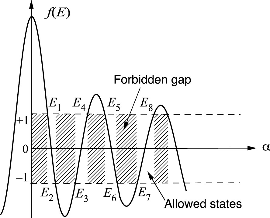
The left-hand side of (3.107) is clearly a function of α which is proportional to $$ \sqrt E $$. Therefore, we can plot f(E) in (3.107) as a function of $$ \sqrt E $$ and impose a limit of –1 ≤ f(E) ≤ 1 to yield the allowed solutions shown in Fig. 3.17. We note that the ordinate is (1 + P) for α = 0, where sin(αa) ≈ αa, and it is ±1 for α equal to any multiple of (π/a), regardless of the value of P. The left side of (3.107) contains a [sin(αa)]/(αa) term, which is a sinc function, with the same periodicity and phase as cos(αa). Since the amplitude of the sinc function decreases quickly with increasing α, its contribution diminishes after a few periods. Therefore, for a small P, the resultant f(E) has a shape similar to cos(αa) beyond several times of (π/a). Note that, consistent with our earlier discussions of the free electron model, the forbidden bands are narrower than the allowed energy bands.
../images/325043_1_En_3_Chapter/325043_1_En_3_Fig17_HTML.png
Fig. 3.17

Plot of the left side of (3.107) for P = 2 as a function of α. The allowed states are located within 1 ≥ f(E) ≥ –1, and the shaded areas are the forbidden regions

In the following, we shall discuss two extreme cases of the nearly free electron model.

  1. (i)

    Case I: P → ∞

     
Since P is a product of (V0b) and a, where (V0b) is finite and small, an infinite P means that the lattice constant (a+b) is near infinity. This is equivalent to the case of discrete atoms. In the range of –1 ≤ f(E) ≤ 1, the only possible solution of (3.107) is when sin(αa) ≈ 0 or αa = ± for n = 1, 2, 3, … We can deduce the allowed energy states as
$$ \alpha = \pm \frac{n\pi }{a} = \sqrt {\frac{2mE}{{\hbar^{2} }}} $$
(3.109)
or
$$ E = \frac{{\hbar^{2} }}{2m}\left( {\frac{n\pi }{a}} \right)^{2} \quad  n = 1, 2, 3, \ldots $$
(3.110)

The allowed E’s are discrete levels as seen in an isolated atom.

  1. (ii)

    Case II: P → 0

     
Since (V0b) is a small and finite, the condition of P approaching zero implies that the lattice constant (a + b) is also near zero. The electron wave functions can easily tunnel through the thin barriers and act like a pool of free electrons. The solution (3.107) reduces to
$$ { \cos }\left( {\alpha a} \right) = { \cos }\left( {ka} \right) $$
(3.111)
or
$$ \alpha = k = \sqrt {\frac{2mE}{{\hbar^{2} }}} $$
(3.112)

Therefore, $$ E = \hbar^{2} k^{2} /2m $$, and the allowed energy states form a continuous band.

  1. (b)

    Tight-binding approximation

     
This approach takes a point of view opposite to that of free electron model. It is based on the assumption that the atoms of the crystal are so far apart that the wave functions for neighboring electrons overlap only to a small extent. If we keep V0 and a fixed and vary d = (a + b), we see that as b becomes large,
$$ \sinh \left( {\gamma b} \right) \approx \cosh \left( {\gamma b} \right) \approx \exp \left( {\gamma b} \right)/2 . $$
(3.113)
Thus the general solution of the Kronig–Penney model becomes
$$ \left[ {\left( {\frac{{\gamma^{2} - \alpha^{2} }}{2\alpha \gamma }} \right)\sin \left( {\alpha a} \right) + \cos \left( {\alpha a} \right)} \right]\frac{{\exp \left( {\gamma b} \right)}}{2} = \cos \left[ {k\left( {a + b} \right)} \right] $$
(3.114)
Since b is a large number and both b and γ are positive, it is clear that |cos[k(a + b)]| ≤1 only if
$$ \left( {\frac{{\gamma^{2} - \alpha^{2} }}{2\alpha \gamma }} \right)\sin \left( {\alpha a} \right) + \cos \left( {\alpha a} \right) = 0 $$
(3.115)
or
$$ { \tan }\left( {\alpha a} \right) \approx \frac{2\alpha \gamma }{{\alpha^{2} - \gamma^{2} }} $$
(3.116)
This equation has an equivalent form of
$$ \left( {\alpha a} \right){ \tan }\left( {\alpha a} \right) \cong \gamma^\prime a $$
(3.117)
for V0 > E, where γ′ is a function of α and γ. This expression is similar to the solution of an isolated finite depth quantum well with a well depth of V0 and a width of 2a. This implies that the allowed energy bands are very narrow in the tight-binding approximation, which leads to a nearly linear relationship between f(E) and E in each allowed narrow energy band. However, as shown in Fig. 3.18, the solution (3.115) still maintains the shape of a sinc function.
../images/325043_1_En_3_Chapter/325043_1_En_3_Fig18_HTML.png
Fig. 3.18

Plot of the left side of (3.115) as a function of α. The allowed states are located within 1 ≥ f(E) ≥ –1, and the shaded areas are the forbidden regions. The allowed energy bands are between E1 and E2, E3 and E4, E5 and E6, etc

We know that in a two-dimensional system, the line equation of a linear function between point 1 at (x1, y1) and point 2 at (x2, y2) can be written as
$$ \frac{{y - y_{1} }}{{x - x_{1} }} = \frac{{y_{2} - y_{1} }}{{x_{2} - x_{1} }} $$
(3.118)
We can apply (3.118) to derive the allowed energy states. In the lowest (first) allowed energy band, between E1 and E2, the line equation can be expressed as
$$ \frac{{f\left( E \right) - f\left( {E_{1} } \right)}}{{E - E_{1} }} = \frac{{f\left( {E_{2} } \right) - f\left( {E_{1} } \right)}}{{E_{2} - E_{1} }} $$
(3.119)

For the allowed energy states, f(E1) = f(E4) = f(E5) = f(E8) = $$ \cdots $$ = +1, f(E2) = f(E3) = f(E6) = f(E7) = $$ \cdots $$ = –1, and f(E) = cos[k(a + b)], which lead to the following results.

In the first allowed energy band, according to (3.119),
$$ \cos \left[ {k\left( {a + b} \right)} \right] - 1 = - 2\left( {\frac{{E - E_{1} }}{{E_{2} - E_{1} }}} \right) $$
(3.120)
If we assume the first allowed energy band width is
$$ \Delta E_{1} = E_{2} - E_{1} $$
(3.121)
then (3.120) can be expressed in terms of ΔE1 as
$$ E = E_{1} + \frac{{\Delta E_{1} }}{2}\left\{ {1 - \cos \left[ {k\left( {a + b} \right)} \right]} \right\} $$
(3.122)
The result of (3.122) is plotted in Fig. 3.19a. Note that, in contrast to the free electron theory, the minimum allowed energy state is a nonzero value.
../images/325043_1_En_3_Chapter/325043_1_En_3_Fig19_HTML.png
Fig. 3.19

Plot of the E-k curve of the a first and b second allowed energy bands using tight-binding approximation

The second allowed energy band is between f(E3) = –1 and f(E4) = +1. The line equation has the form of
$$ \cos \left[ {k\left( {a + b} \right)} \right] + 1 = 2\left( {\frac{{E - E_{3} }}{{E_{4} - E_{3} }}} \right) $$
(3.123)
This is rearranged below to show the allowed energy function.
$$ E = E_{3} + \frac{{\Delta E_{2} }}{2}\left\{ {1 + { \cos }\left[ {k\left( {a + b} \right)} \right]} \right\} $$
(3.124)
where ΔE2 = E4E3. This cosine function (3.124) is plotted in Fig. 3.19b. Using this process for higher energy bands, we can construct the complete energy band diagram. In Fig. 3.20, we note that there are discontinuities at k = ±nπ/a, where energy gaps exist. The minimum allowed energy state is not zero and has a finite value. At higher energies, the allowed states become wider.
../images/325043_1_En_3_Chapter/325043_1_En_3_Fig20_HTML.png
Fig. 3.20

Plot of the E-k curve according to the tight-binding approximation (solid curves) compared with the free electron mode (long-dashed curves). The reduced zone representation is plotted as short-dashed curves

3.5 Effective Mass

Before we move on to examine the realistic energy band structure of common semiconductors, let us now consider the motion of an electron in the crystal under the influence of an applied electric field. First, if the Bloch function uk(z) in (3.39) is set to be a constant, then the wave function has the form of exp(±ikz), corresponding to a perfectly free electron of momentum p = ћk whose energy would be
$$ E = \frac{{\hbar^{2} k^{2} }}{2m} $$
(3.125)
where k is a propagation constant. This relation is shown as the long-dashed curve in Fig. 3.20. Under this condition, pћk is the crystal momentum and has a value close to the real momentum of a moving particle. However, in a real crystal, the nonzero periodic potential function leads to discontinuities in the E-k curve at k = ±/d. The true instantaneous momentum of an electron is no longer a constant of the motion, while the crystal momentum ћk is a perfectly well-defined constant value for a given energy state. Since there exist allowed wave functions with different k’s, we shall use the group velocity to relate the electron ‘wave packet’ following
$$ \upsilon_{g} = \frac{{{\text{d}}\omega }}{{{\text{d}}k}} = \frac{1}{\hbar }\frac{{{\text{d}}E}}{{{\text{d}}k}} $$
(3.126)
where E = ћω. Again, this equation shows that the instantaneous momentum of the traveling electrons at the Brillouin zone boundaries is no longer a constant of the motion.
Suppose an electric field F is applied such that, over a distance dz in a period dt, the group velocity of the electron increases by dυg. The rate of change of electron energy due to the applied field is
$$ {\text{d}}E = - qF{\text{d}}x = - qF\upsilon_{g} {\text{d}}t $$
(3.127)
Then, using (3.126) and (3.127) we see that
$$ {\text{d}}E = \frac{{{\text{d}}E}}{{{\text{d}}k}}{\text{d}}k = - \frac{qF}{\hbar }\frac{{{\text{d}}E}}{{{\text{d}}k}}{\text{d}}t $$
(3.128)
Therefore,
$$ {\text{d}}k = - \frac{qF}{\hbar }{\text{d}}t $$
(3.129)
or
$$ \hbar \frac{{{\text{d}}k}}{{{\text{d}}t}} = \frac{{{\text{d}}p}}{{{\text{d}}t}} = - qF = {\mathcal{F}} $$
(3.130)
where p is the crystal momentum. Equation (3.130) indicates simply that the time rate of change of crystal momentum equals the force, $$ {\mathcal{F}} $$. Thus it is the analogue of Newton’s law, showing that the crystal momentum of the electron in a periodic lattice changes under the influence of an applied electric field in the same way as does the true momentum of a free electron in free space.
Differentiating (3.126) with respect to time, the result is
$$ \frac{{{\text{d}}\upsilon_{g} }}{{{\text{d}}t}} = \frac{1}{\hbar }\frac{\text{d}}{{{\text{d}}t}}\left( {\frac{{{\text{d}}E}}{{{\text{d}}k}}} \right) = \frac{1}{\hbar }\frac{{{\text{d}}^{2} E}}{{{\text{d}}k^{2} }}\left( {\frac{{{\text{d}}k}}{{{\text{d}}t}}} \right) = \frac{1}{{\hbar^{2} }}\frac{{{\text{d}}^{2} E}}{{{\text{d}}k^{2} }}\left( {\hbar \frac{{{\text{d}}k}}{{{\text{d}}t}}} \right) $$
(3.131)
Using (3.130), the magnitude of acceleration a can be written as
$$ a = \frac{{{\text{d}}\upsilon_{g} }}{{{\text{d}}t}} = \frac{1}{{\hbar^{2} }}\frac{{{\text{d}}^{2} E}}{{{\text{d}}k^{2} }}\left( {\hbar \frac{{{\text{d}}k}}{{{\text{d}}t}}} \right) = \frac{{\mathcal{F}}}{{m^{*} }} $$
(3.132)
where the effective mass m* is defined as
$$ m^{*} \equiv \frac{{\hbar^{2} }}{{\left( {{\text{d}}^{2} E/{\text{d}}k^{2} } \right)}} $$
(3.133)
or
$$ m^{*} = \left( {\frac{1}{{\hbar^{2} }}\frac{{\partial^{2} E}}{{\partial k_{i} \partial k_{j} }}} \right)^{ - 1} $$
(3.134)
for the non-spherical constant energy surface case. We can check this concept in a free electron system with mass m0 where
$$ E = \frac{{\hbar^{2} k^{2} }}{{2m_{0} }},\frac{{{\text{d}}E}}{{{\text{d}}k}} = \frac{{\hbar^{2} k}}{{m_{0} }},\;{\text{and}}\;\frac{{{\text{d}}^{2} E}}{{{\text{d}}k^{2} }} = \frac{{\hbar^{2} }}{{m_{0} }} $$
Then the effective mass simply equals the free electron mass as expected, i.e.,
$$ m^{*} = \frac{{\hbar^{2} }}{{\left( {{\text{d}}^{2} E/{\text{d}}k^{2} } \right)}} = m_{0} $$
(3.135)
To further illustrate the relationship between the E-k curve, group velocity, and m*, a tight-binding limit model is used for two specific simple E(k) variations in Fig. 3.21.
../images/325043_1_En_3_Chapter/325043_1_En_3_Fig21_HTML.png
Fig. 3.21

Variation of a, d electron energy, b, e electron velocity, and c, f effective mass with reduced wave vector for states in a band of one-dimensional crystal. The E-k curve is a cosine function for the left panel, and in the form of (1 + coska) for the right panel

Assume, in one case, that
$$ E = \left( {\Delta E/2} \right)\left( {1 - \cos kd} \right) $$
(3.136)
It represents the E-k dispersion curve of the lowest band, where ΔE is the allowed energy bandwidth. Under an applied electric field, the group velocity and effective mass are calculated as
$$ \upsilon_{g} = \frac{1}{\hbar }\left( {\frac{{{\text{d}}E}}{{{\text{d}}k}}} \right) = \frac{{{d}\Delta E}}{2\hbar }\sin kd $$
(3.137)
and
$$ m^{*} = \frac{{\hbar^{2} }}{{\left( {{\text{d}}^{2} E/{\text{d}}k^{2} } \right)}} = \frac{{2\hbar^{2} }}{{{d}^{2} \Delta E}}{ \sec }kd $$
(3.138)
As shown in Fig. 3.21b, the resultant group velocity is not a constant within the first Brillouin zone. Rather, it oscillates from zero to a maximum, then going through a minimum and back up to maximum again. Since the zone boundaries ±π/d are equivalent using the periodicity of k-space, the zero velocity at the zone boundaries corresponds to the standing wave nature of the electron waves due to Bragg reflections. Furthermore,
$$ \begin{aligned} x\left( t \right) = \int \upsilon_{g} \left( t \right){\text{d}}t &amp; = \frac{\Delta E}{2qF}\left[ {1 - \cos \left( {\frac{qFtd}{\hbar }} \right)} \right] \\ &amp; = \frac{\Delta E}{2qF}\left( {1 - \cos kd} \right) \\ \end{aligned} $$
(3.139)
where k = (qFt)/ħ. The results of (3.137) and (3.139) show that electrons oscillate in both k- and real space, rather than accelerating uniformly as they would do the absence of a periodic potential.

This velocity oscillation is equivalent to a mass change at critical points in k-space shown in Fig. 3.21c. The electron mass has a constant positive value near the zone center but becomes negative on the zone boundary. One unusual property of the effective mass is that at wave vectors corresponding to the maximum and minimum velocities, the effective mass goes to infinite. This marks the point where a deceleration must begin to slow down the electron. The other peculiar property is that the effective mass has regions in which it is negative. A negative m* means that the acceleration resulting from the externally applied electric field is in a direction opposite to that of the applied field; this is the effect of electron reflection due to the periodic crystal lattice.

In the second tight-binding limit model, as shown in Fig. 3.21d, the E(k) variation can be represented by
$$ E = \left( {\Delta E^\prime /2} \right)\left( {1 + \cos kd} \right) $$
(3.140)

It resembles the E-k curve of the valence band in a semiconductor with an allowed energy bandwidth of ΔE′. By the same procedures, we can derive the group velocity and effective mass as displayed in Fig. 3.21e, f, respectively.

The E-k dispersion curve shown in Fig. 3.21a is very much like the conduction band edge of a direct bandgap semiconductor such as GaAs. We shall use it to discuss some properties related to semiconductor materials. Since the electron effective mass is a function of k within the first Brillouin zone, what value of k should be used for determining m*? Ideally, in a perfect crystal, under the influence of an applied electric field, the electron takes a periodic motion indefinitely within the first Brillouin zone as described by (3.137) and (3.139). This is known as the Bloch oscillation with a frequency ω = qFd/ħ, and there have been many attempts to observe and utilize it as a possible terahertz (THz) radiation source. However, all attempts to observe Bloch oscillation in conventional bulk solids have failed. For all reasonable applied fields, the Bloch oscillation is destroyed by scattering with impurities, defects, and phonons, before a single oscillation cycle is completed. The existence of such periodic oscillations in THz (1 THz = 1012 Hz) range was finally experimentally observed in 1993 in a semiconductor superlattice structure [2]. The multiple periods of GaAs/AlGaAs thin layers form superlattices that have a lattice periodicity much larger than the lattice constant of GaAs. This large lattice periodicity reduces the width of the Brillouin zone in k-space such that the scattering loss is suppressed. Therefore, in real semiconductors, the electron only travels a short range of the periodic E-k curve due to scattering events. The two dominant scattering processes are phonon scattering due to lattice vibration, and impurity and defect scattering. In high quality semiconductor materials, phonon scattering dominates the carrier relaxation process near room temperature and above. Through these processes, an electron can lose its energy quickly and move to the zone center of the E-k curve where the potential energy is the lowest. Near the zone center, the energy can be approximated by a parabolic function of k or E = A(kk0)2. The effective mass has a constant value of m* = ħ2/2A, and the dynamical behavior of the electron will be the same as that of a free particle with this effective mass. For indirect bandgap semiconductors like Si and Ge, although the minimum conduction band edge is not located at the Γ point, the energy is still a parabolic function of k. The effective mass will also be a constant similar to that of the direct bandgap material.

3.6 Band Structures of Common Semiconductors
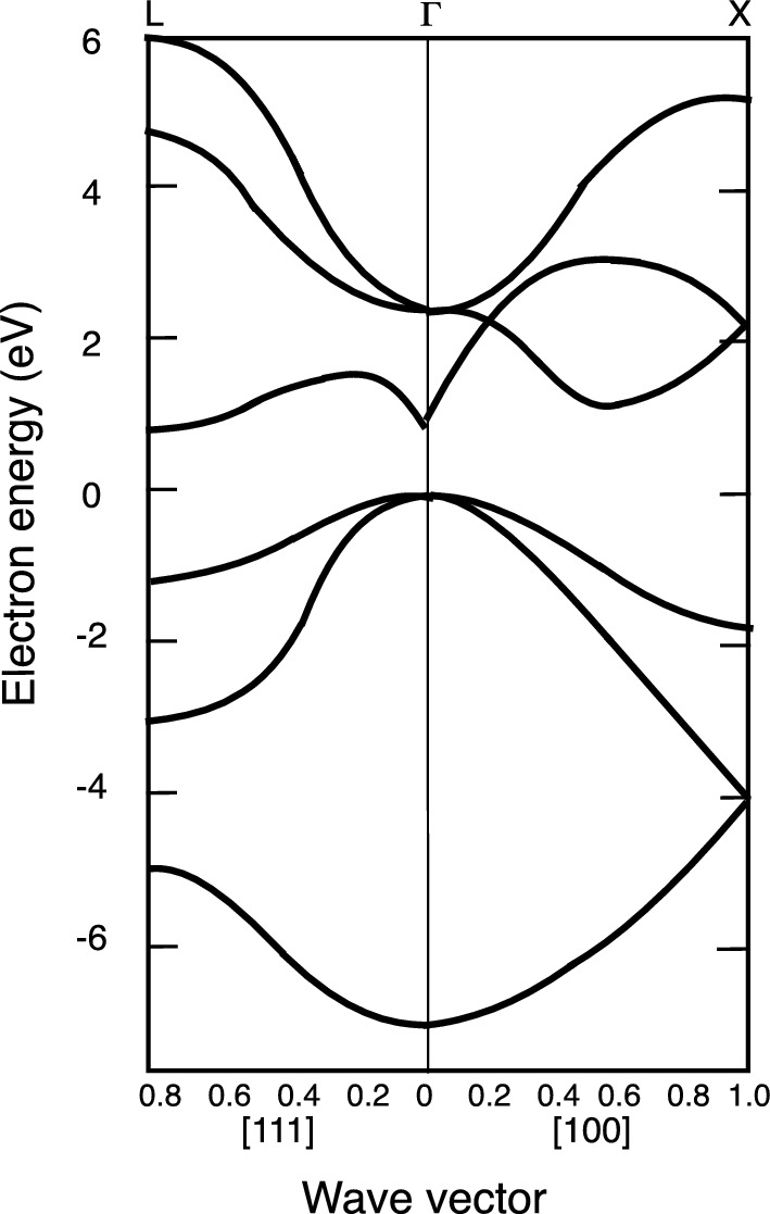
The introduction of the lattice influence in terms of a small periodic potential function in a 1D nearly free electron system leads to the development of the energy bandgap concept. When we move from the 1D to the 3D nearly free electron system incorporating the effect of a small periodic potential, we encounter not only the increased dimension but also new possibilities that arise with the availability of more dimensions. For example, for an electron moving through a 3D crystal, an energy bandgap in one k-direction may be bridged by an allowed band in another k-direction. This possibility of the 3D system gives rise to the existence of overlapping bands, which is not possible in a 1D system. Typical energy bands for a diamond structure crystal are shown in Fig. 3.22. These E-k curves may be compared with the empty lattice model of a FCC crystal given in Fig. 3.12.
../images/325043_1_En_3_Chapter/325043_1_En_3_Fig22_HTML.png
Fig. 3.22

Typical energy bands for a diamond-like crystal structure.

Reprinted with permission from [3], copyright Wiley

3.6.1 General Trend of Energy Band Structure in Semiconductors
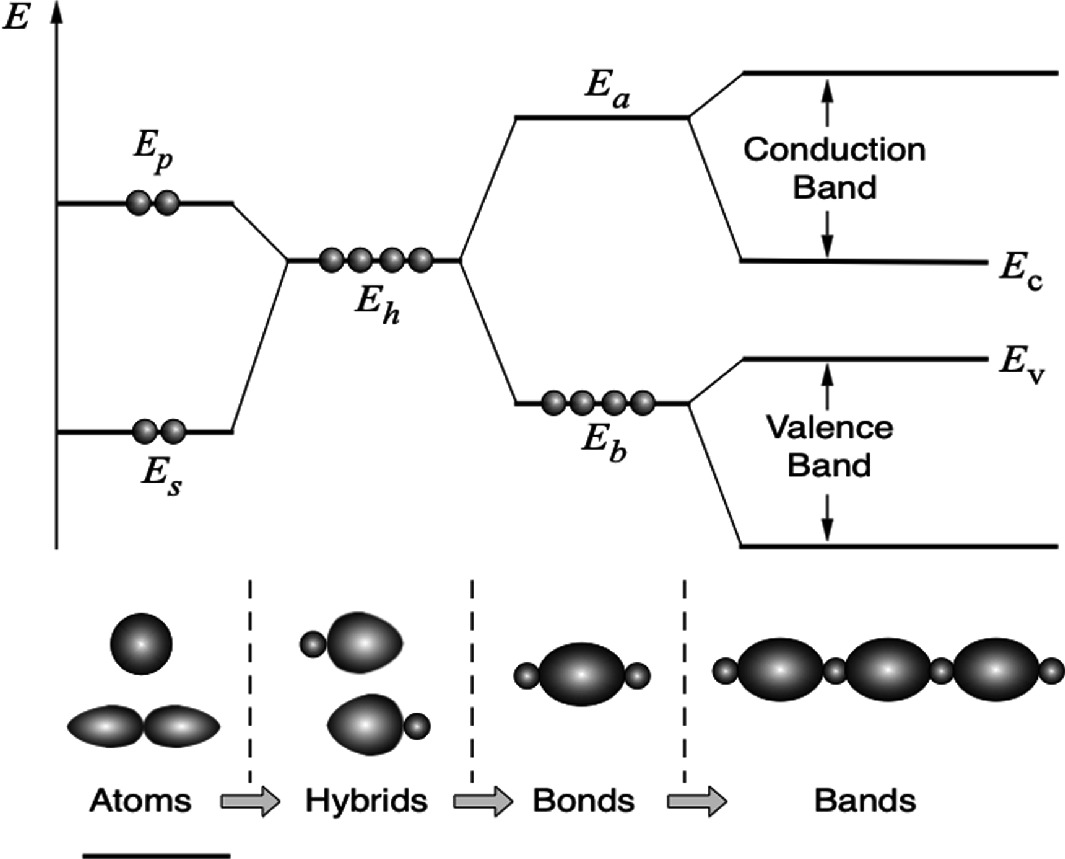
The tetrahedral bonds of diamond and zinc-blende semiconductor structures are derived from the sp3 hybrid orbit. By linear combination of spherically symmetric s-like waves with three directional p-like waves, as expressed in (2.24), four sp3 hybrids are produced. These four sp3 hybrid orbitals form a tetrahedron bond structure, which is the basic arrangement of all semiconductor crystals. Figure 3.23 shows schematically the evolution of the s- and p-like atomic states to the conduction and valence bands in hybridized elemental semiconductor systems. Atomic s- and p-states are hybridized to form sp3 hybrid bonds which then can form bonding and anti-bonding combinations between orbitals on neighboring atoms pointing along the common bond. Finally, these molecular orbitals associated with bonding and anti-bonding levels become broadened into bands by interactions between hybrid orbitals on the same atom, the valence band being formed from bonding orbitals and the conduction band from anti-bonding orbitals. Therefore, the states are purely s-like or p-like. At the zone center (Γ-point), the bottom of the valence band is therefore s-like, and the top is p-like and triply degenerated when spin-orbit coupling is neglected. Similarly, at Γ-point, the bottom of the conduction band is purely s-like. The development of the energy band structure for a polar (compound) semiconductor proceeds in the same way. Hybrids are formed on both atom types and then form bonding and anti-bonding states with the other hybrid in the bond. Finally, the valence and conduction bands are formed from the broadened bonding and anti-bonding levels.
../images/325043_1_En_3_Chapter/325043_1_En_3_Fig23_HTML.png
Fig. 3.23

Development of energy band structure of silicon. The single s-states (Es) and p-states (Ep) on each atom are transformed to four hybrid states (Eh), which are combined with neighboring hybrids to form bonds. The bonding (Eb) and anti-bonding (Ea) levels finally broaden into energy bands in the crystal

Using Ge as an example, the true energy bands and the nearly free electron bands are compared in Fig. 3.24. The true bands are obtained by combining pseudopotential calculations with experimental optical measurement data. The nearly free electron-like bands in Fig. 3.24b are remarkably similar to those at the bottom of the valence band and the upper part of the conduction band of the ‘true’ band structure (Fig. 3.24a), except that bandgaps at certain critical points in the Brillouin zone do not occur in the nearly free electron band structure. The other feature displayed in Fig. 3.24 is that Ge is an indirect bandgap semiconductor. Its maximum of the valence band is located at Γ, and the minima in the conduction band are located in the $$ \left\langle {111} \right\rangle $$ directions at the L-point. On the other hand, GaAs is a direct bandgap semiconductor with both the maximum of the valence band and the minimum of the conduction band located at the Γ-point. Therefore, it is instructive to examine the trends in the band structures of tetrahedrally bonded semiconductors, specifically the III–V compounds exhibiting mixed ionic-covalent bonding.
../images/325043_1_En_3_Chapter/325043_1_En_3_Fig24_HTML.png
Fig. 3.24

Energy bands of germanium. a Energy band obtained by pseudopotential calculations. Reprinted with permission from [4], copyright American Physical Society, b energy band calculated using the nearly free electron model
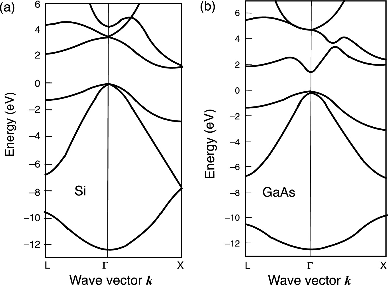
For group IV elements, there is an increase in metallic tendency (metallicity) on going from C to Sn when increasing the atomic number. With increasing metallicity, as expected, the conduction band minimum at the Γ-point drops faster than at X or L. At some point, the semiconductor turns into direct bandgap material. Indeed the indirect bandgaps of diamond, silicon and germanium turn into direct in α-Sn. This trend is also true for III–V compounds. The lowest conduction band drops more quickly at the Γ-point than at X or L with increasing metallicity, so the III–V compounds become direct bandgap semiconductors. The Al-compounds and GaP are the exceptions with indirect bandgaps. The energy band structures of Si and GaAs are shown in Fig. 3.25. On the other hand, for III–V compounds, there is an increase in ionicity which has a tendency to increase the bandgap energy. For example, the III–V nitride compounds with wurtzite crystal structure have bandgap energies much larger than 2 eV.
../images/325043_1_En_3_Chapter/325043_1_En_3_Fig25_HTML.png
Fig. 3.25

Detailed energy band structures of a Si and b GaAs.

Reprinted with permission from [4], copyright American Physical Society

3.6.2 Valence Band

Consider the pz-orbit in a cubic crystal. As shown in Fig. 3.26a, the wave functions are polarized along the z-direction. Electrons move easily along the z-direction. This corresponds to a light effective mass shown as the E-k curve with a small radius of curvature (Fig. 3.26b). On the other hand, electrons moving in x- and y-directions are very restricted and have a heavy effective mass, shown as the slow varying E-k curve. The same property can be said about px- and py-like orbits. The combined 3D E-k diagram of the valence band turns out to be a complex composition. As shown in Fig. 3.27, there are heavy-hole, light-hole, and split-off bands. The maximum of the heavy- and light-hole bands degenerate at k = 0. Away from the Γ-point, the heavy- and light-hole bands with different radii of curvature in the E-k curve result. Near the zone center, they can be described as
$$ E\left( k \right) = E_{v} - \frac{{\hbar^{2} k^{2} }}{{2m_{0} m_{\text{h}} }} $$
(3.141)
where mh equals mhh or mlh for heavy holes or light holes, respectively. Although widely used for its simplicity and convenience, it must be stressed that this approximation is valid only near the vicinity of the zone center. In realistic situations, the bands are both non-parabolic and anisotropic, depending on the direction of k as well as its location from the zone center. The simple spherical surfaces predicted by (3.141) are modified into complex warped spheres. The non-spherical hole dispersion relation near the zone center can be described by Luttinger parameters. The situation becomes even worse if the cubic symmetry is broken by introducing strain in the material.
../images/325043_1_En_3_Chapter/325043_1_En_3_Fig26_HTML.png
Fig. 3.26

Valence band constructed from pz orbitals. a Regular arrangement of pz orbitals. b E-k curves of pz orbitals only; the band is ‘light’ along kz and ‘heavy’ along kx or ky

../images/325043_1_En_3_Chapter/325043_1_En_3_Fig27_HTML.png
Fig. 3.27

Total band structure at the top of the valence band for tetrahedral semiconductors

The decoupling of the spin-orbit split-off band from the top of the valence band is caused by the interaction of the electron spins (s = ±1/2) of the valence electrons with the magnetic moment (l = 1 for p-state) arising from their orbital motion, which yield a total angular momentum j = l + s = 3/2 and 1/2. The separation between the top of the heavy-/light-hole bands and the spin-orbit split-off band, Δso, increases with atomic number, essentially because the greater the nuclear charge, the greater the internal magnetic field experienced by the orbiting electron. Thus, Δso is very small for Si (0.04 eV), fairly large for GaAs (0.34 eV), and quite large for InSb (0.81 eV).

3.6.3 Conduction Band

  1. (a)

    Direct bandgap materials

     
The conduction band originates from s-like orbitals which have a spherical symmetry. For III–V compounds such as GaAs , the conduction band minimum is located at the zone center (Γ-point), and these are called direct bandgap semiconductors . Near the conduction band minimum , the band can be described by
$$ E\left( k \right) = E_{\text{c}} + \frac{{\hbar^{2} k^{2} }}{{2m_{0} m_{\text{e}} }} $$
(3.142)

Thus the constant energy surface of the conduction band has a spherical shape. For direct bandgap semiconductors, the radius of the E-k curve of the lowest conduction band is relatively small, leading to a light electron effective mass. In GaAs, $$ m_{\text{e}}^{*} $$ ≅ 0.063m0 is the electron effective mass.

  1. (b)

    Indirect bandgap materials

     
For indirect bandgap semiconductors , the shape of the lowest conduction band minimum is more complex. In Si (and diamond), the minima are located along $$ \left\langle {100} \right\rangle $$ about 85% of the way to the X-zone boundary. As illustrated in Fig. 3.28, there are six Δ-directions and, therefore, six equivalent minima in a cubic crystal. Due to their off-center location, these minima (valleys) have anisotropic E-k relationships along kx, ky, and kz.
$$ E\left( k \right) = E_{\text{c}} + \frac{{\hbar^{2} }}{{2m_{0} }}\left[ {\frac{{\left( {k_{x} - k_{0} } \right)^{2} }}{{m_{\text{L}} }} + \frac{{k_{y}^{2} }}{{m_{\text{T}} }} + \frac{{k_{z}^{2} }}{{m_{\text{T}} }}} \right] $$
(3.143)
where the subscripts L and T indicate longitudinal and transverse components, respectively. In Si , mL = 0.92 and mT = 0.19. As mentioned earlier, Ge also has indirect bandgap with the conduction band minima along $$ \left\langle {111} \right\rangle $$ in the L-point. In Ge , as shown in Fig. 3.29, there are eight ellipsoidal equivalent valleys located at the zone boundaries where mL = 1.59 and mT = 0.082. Since only half of the constant energy surface is located inside the first Brillouin zone, the degenerate factor g is 4, not 8.
../images/325043_1_En_3_Chapter/325043_1_En_3_Fig28_HTML.png
Fig. 3.28

a The Brillouin zone of Si with six equivalent constant energy surfaces along Δ-direction. b Enlarged view of one of the constant energy volumes, showing longitudinal and doubly degenerated transverse masses mL and mT, respectively
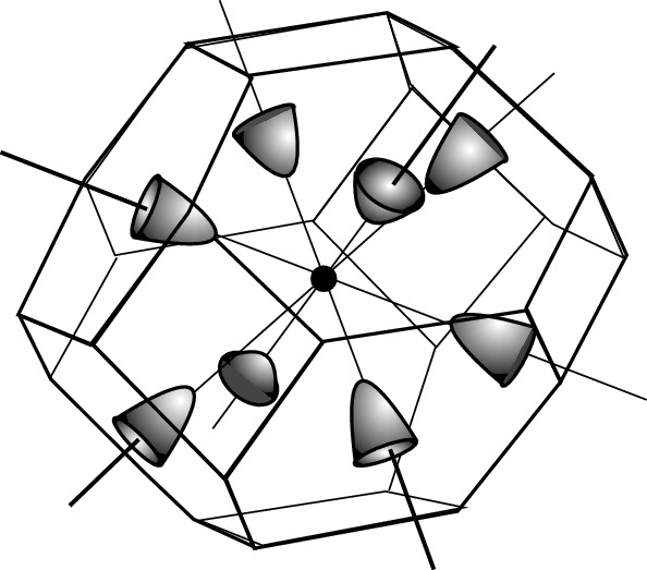
../images/325043_1_En_3_Chapter/325043_1_En_3_Fig29_HTML.png
Fig. 3.29

Brillouin zone of Ge with constant energy surfaces for the eight equivalent L-valleys

3.6.4 Band Structures of Wurtzite Crystals

Although the crystal structure of most III–V compounds is zinc-blende, the III-nitride alloys prefer the formation of wurtzite crystal structure. Since both structures are characterized by the tetrahedral lattice arrangement, as discussed in Sect. 2.​4, the nearest-neighbor environments are identical with only slight differences in the next nearest-neighbor arrangements. It is necessary to go beyond next nearest neighbors before both positional and directional differences occur. One can regard the wurtzite structure along the c-axis as a cubic zinc-blende lattice slightly deformed along the body diagonal of [111]. Figure 3.30 compares the Brillouin zone of zinc-blende and wurtzite crystal structures. A correspondence is obtained between the [111] direction ΓL in zinc-blende structure and the [0001] direction ΓΓ′ in wurtzite. Therefore, a strong similarity between the band structure of zinc-blende and wurtzite crystals can be expected. However, in contrast to the more symmetric cubic zinc-blende crystal, the in-plane (basal plane) behavior of the energy bands is different from the behavior along the [0001] axis (the c-axis) in wurtzite crystal. The anisotropic hexagonal structure, when including spin-orbit interaction, leads to energy splitting in the valence band edges. The valence band structure for GaN is shown in Fig. 3.31. The heavy-hole (HH) and light-hole (LH) bands no longer degenerate at k = 0 and separated by the spin-orbit interaction (Δso). The crystal-hole (CH) valence band results from the crystal-field splitting energycr). The topmost three valence band energy levels at k = 0 (E1, E2, and E3, in decreasing order) are
$$ E_{1} = \Delta_{1} + \Delta_{2} $$
(3.144a)
$$ E_{2} = \frac{{\Delta_{1} - \Delta_{2} + \sqrt {\left( {\Delta_{1} - \Delta_{2} } \right)^{2} + 8\Delta_{3}^{2} } }}{2} $$
(3.144b)
$$ E_{3} = \frac{{\Delta_{1} - \Delta_{2} - \sqrt {\left( {\Delta_{1} - \Delta_{2} } \right)^{2} + 8\Delta_{3}^{2} } }}{2} $$
(3.144c)
where E1 is labeled as HH band, E2 is labeled as LH band, and E3 is labeled as CH band. We also assumed
$$ \Delta_{1} = \Delta_{\text{cr}},\;\Delta_{2} = \Delta_{3} = \Delta_{\text{so}} $$
(3.145)
../images/325043_1_En_3_Chapter/325043_1_En_3_Fig30_HTML.png
Fig. 3.30

Brillouin zone of zinc-blende and wurtzite-type materials.

Reprinted with permission from [5], copyright American Physical Society

../images/325043_1_En_3_Chapter/325043_1_En_3_Fig31_HTML.png
Fig. 3.31

Valence band structure of wurtzite GaN.

Reprinted with permission from [6], copyright AIP Publishing

In general, Δcr and Δso have positive values for III-nitrides except that AlN has a negative Δcr. Thus, the top valence band of AlN is E2 instead, and the valence bands from top to bottom are CH, HH, and LH, respectively. Note that the valence band energy splitting E1E2 and E1E3 are measurable quantities through inter-band optical transition measurements whereas Δcr and Δso are parameters of theory, obtainable indirectly by fitting experimental energy splitting.

All III-nitride semiconductor alloys have direct bandgaps. The bottom of the conduction band in GaN and InN is well approximated by a parabolic dispersion relationship, while a greater anisotropy in AlN than GaN is predicted due to the reduced lattice symmetry. The conduction band-edge energy is deduced by adding the bandgap energy to E1.
$$ E_{\text{c}} = E_{\text{g}} + \Delta_{1} + \Delta_{2} $$
(3.146)
Problems
  1. 1.

    Calculate the first two E-k curves along the [110] axis for a BCC crystal using the 3D free electron model.

     
  2. 2.
    For an artificial two-dimensional square lattice structure shown below, calculate the first two energy bands for free electrons along the Γ-X, X-K, and Γ-K directions.
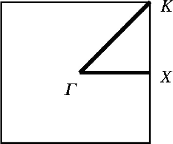
    ../images/325043_1_En_3_Chapter/325043_1_En_3_Figa_HTML.png
     
  3. 3.

    Calculate and plot the density of states as a function of energy in the conduction band of a GaAs/AlGaAs quantum well for the first three bound states located at 25, 100, and 225 meV above the conduction band edge. The electron effective mass of GaAs in the conduction band is m* = 0.067m0.

     
  4. 4.

    Derive the density of states for a quantum dot system. In a quantum dot system, the quantum confinement is three-dimensional.

     
  5. 5.

    Suppose the E-k relation is given by $$ E = E_{0} + \left( {\Delta E/2} \right)\left( {1 - \cos ka} \right) $$. For very small k. prove that the parabolic approximation holds and determines the effective mass.

     
  6. 6.
    For the delta function periodic potential (V0 ~ ∞, b ~ 0 and V0b is small but finite or P ≪ 1), use the Kronig–Penney model to calculate
    1. (a)

      The energy of the lowest energy band at k = 0.

       
    2. (b)

      The bandgap at k = π/a.


  7. 7.

    Derive the following solution of the Kronig–Penney model for a crystal:

    $$ - \left( {\frac{{\alpha^{2} + \beta^{2} }}{2\alpha \beta }} \right)\sin \left( {\alpha a} \right)\sin \left( {\beta b} \right) + \cos \left( {\alpha a} \right)\cos \left( {\beta b} \right) = \cos \left[ {k\left( {a + b} \right)} \right] $$
    by setting the determinant of wave functions (3.101) to zero.
     
  8. 8.

    Consider a simple cosine approximation to the shape of an energy band as

    $$ E\left( k \right) = \frac{\Delta E}{2}\left( {1 - \cos ka} \right). $$
    1. (a)

      For small k, prove that the parabolic approximation holds and $$ \upsilon \left( k \right) \cong \hbar k/m^{*} $$.

       
    2. (b)

      Many semiconductors have a saturation velocity for electrons of around 107 cm/s. How much of the first Brillouin zone do electrons need to explore to reach this velocity? Assume the initial position of electrons is at the zone center. For calculations, use the velocity equation of part (a) and the following material parameters of GaAs: m* = 0.067m0 and lattice constant a0 = 5.653 Å.


  9. 9.
    Consider a single electron in a perfect crystal. Starting from k = 0 in an empty band, the electron is accelerated by a constant electric field –F toward +k. Assume $$ E = \left( {\Delta E/2} \right)\left( {1 - \cos ka} \right) $$ and $$ \hbar k = \left( {qF} \right)t = {\mathcal{F}}t $$.
    1. (a)

      Find the velocity of the electron.

       
    2. (b)

      Prove that the position of the electron in real space as a function of time is

      $$ x\left( t \right) = \frac{\Delta E}{2qF}\left[ {1 - \cos \left( {\frac{qFa}{\hbar }} \right)t} \right] $$

      The electron oscillates in real space, rather than accelerating uniformly as in the free electron model. This periodic motion of an electron in a periodic crystal structure is called the Bloch oscillation.

       
    3. (c)

      The Bloch oscillation frequency is $$ \omega = qFa/\hbar $$. For F = 108 V/m, calculate the Bloch oscillation frequency in GaAs.

       
    4. (d)

      In semiconductors, due to scattering with defects, the Bloch oscillation of electrons in the Brillouin zone cannot be observed. Assuming the average electron can only travel one tenth of the first Brillouin zone, design a GaAs/AlAs superlattice structure such that the Bloch oscillation can be measured. The lattice constants of GaAs and AlAs are 5.653 Å and 5.660 Å, respectively.