© Springer Nature Switzerland AG 2020
K. Y. ChengIII–V Compound Semiconductors and DevicesGraduate Texts in Physicshttps://doi.org/10.1007/978-3-030-51903-2_9

9. Heterostructure Electronic Devices

Keh Yung Cheng1, 2  
(1)
Department of Electrical and Computer Engineering, University of Illinois at Urbana-Champaign, Urbana, Illinois, USA
(2)
Department of Electrical Engineering, National Tsing Hua University, Hsinchu, Taiwan
 
 
Keh Yung Cheng

Abstract

Compound semiconductors are excellent candidates for high-speed device applications due to their high electron mobility, the ability to form heterostructures, and the availability of semi-insulating substrates. However, the multicomponent nature and the lack of robust native oxides make the fabrication of compound semiconductor-based metal-oxide-semiconductor field-effect transistors (MOSFETs) an extremely difficult task. Instead, GaAs-based metal–semiconductor field-effect transistors (MESFET) were developed initially. A MESFET utilizes a metal–semiconductor Schottky barrier to replace the MOS gate structure. The charge carriers in the active region (channel) are separated spatially from the control (gate) electrode by a depletion layer formed on the semiconductor surface. Nevertheless, due to the nature of the Schottky barrier and high electron mobility, only n-channel MESFETs were studied and the devices are leaky at high positive biases. With the advancements of epitaxial growth technology and new device concepts, efficient advanced devices were developed. Among many three-terminal device structures, the modulation-doped field-effect transistor (MODFET), or high-electron-mobility transistor (HEMT), and the heterojunction bipolar transistor (HBT) are the most widely used high-speed devices. In this chapter, after a brief review of the MESFET, the development and working principles of HEMTs and HBTs are discussed in great detail. Then the key concepts of achieving an oxide-semiconductor interface with low interface state density necessary for the fabrication of high performance III–V MOSFETs are discussed.

The HEMT is a voltage-controlled majority carrier device. It shares the same device geometry as the MESFET except for the details of the active region. The control electrode (gate) is coupled to the active region of the device through a capacitor. The conduction carriers, in the form of the two-dimensional electron gas (2DEG), in the active region are generated by modulation doping at the heterostructure interface.

The structure of the HBT is similar to that of the homostructure bipolar junction transistor (BJT), with the emitter–base junction replaced by a heterojunction. With properly designed heterojunctions, the device parameters such as doping level and layer thickness can be individually optimized for high-speed and high-gain operations. The HBT is a current-controlled minority carrier device with the charged carriers being separated energetically by the energy barriers. The control electrode (base) is resistively coupled to the active device region. The major device attributes of FETs and BJTs are compared in Table 9.1.
Table 9.1

Comparison of BJT and FET


Carriers

Transport

Output control

Input impedance

BJT

Minority

Diffusion

Base current

Low

FET

Majority

Drift

Gate voltage

High

In late 1990, the inversion-mode GaAs MOSFET with a low interface trap density was finally achieved using in situ electron beam evaporated Ga2O3(Gd2O3) dielectric film on MBE GaAs. Next, using ex situ atomic layer deposited high-κ Al2O3 and HfO2 films as the gate dielectric, similar devices were demonstrated on GaAs and other III–V materials. Further refinement of oxide deposition methods and development of additional high-κ gate dielectrics were exploited in the following two decades. At the moment, III–V MOSFET manufacturing technologies are still under development.

9.1 Metal–Semiconductor Field-Effect Transistors (MESFETs)

9.1.1 Basic Operation Principles
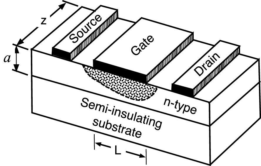
As a prelude to the HEMT, the device characteristics of the MESFET are discussed first. The operating principle of the MESFET is identical to that of a junction FET, and its structure is also similar except that the pn junction is replaced by the Schottky barrier. Most MESFETs use n-type III–V compound semiconductors for the conduction channel because of their high electron mobility and large Schottky barrier height. To minimize the parasitic capacitance, semi-insulating substrates are usually used. A schematic diagram of the MESFET is shown in Fig. 9.1. The active region of the device has a conduction channel thickness a, a gate length L, and a gate width Z. The depletion region has a non-uniform thickness of W(x) along the channel under a large drain bias voltage.
../images/325043_1_En_9_Chapter/325043_1_En_9_Fig1_HTML.png
Fig. 9.1

Schematic structure and dimension of a metal–semiconductor FET. The shaded region is the depletion region under the gate electrode
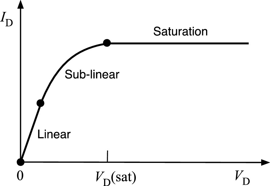
Under normal operation, the source is grounded, the gate is reverse-biased to modulate the conduction channel, and the drain contact is biased at a proper voltage to collect majority carriers. The effect of the applied drain voltage, VD, with the gate open, on the current–voltage relationship is investigated first. When a small positive VD is applied with VGS = 0, the channel of the MESFET is essentially a uniform resistor with a cross-sectional area determined by the width of the device (Z) and the non-depleted channel thickness (aW). The channel current ID is a linear function of the drain voltage as shown in Fig. 9.2. The depletion width along the conduction channel has a constant value of
../images/325043_1_En_9_Chapter/325043_1_En_9_Fig2_HTML.png
Fig. 9.2

General form of the current–voltage characteristics of a MESFET. The pinch-off point defines the saturation drain voltage, VD(sat)

$$ W = \sqrt {\frac{2\epsilon }{{qN_{d} }}V_{0} } $$
(9.1)
where V0 is the contact potential of the Schottky barrier gate, Nd is the carrier concentration of the channel, and $$ \epsilon $$ is the permittivity of the semiconductor.
When a moderate VD of a few tenths of a volt is applied with VGS = 0, the VD simultaneously reverse biases the gate–drain metal–semiconductor junction and widens the depletion region near the drain contact. The depletion region width increases along the conduction channel from source to drain. The depletion width closest to the drain contact becomes
$$ W = \sqrt {\frac{2\epsilon }{{qN_{d} }}\left( {V_{0} + V_{\text{D}} } \right)} $$
(9.2)
The narrowing of the conduction channel leads to an increased channel resistance. The increasing of channel current ID deviates from the linear relationship with increasing VD. Continuing to increase VD causes an ever-increasing depletion of the channel. Eventually, the conduction channel vanishes near the drain contact, where the depletion width approaches the channel width for VGS = 0.
$$ W = \sqrt {\frac{2\epsilon }{{qN_{d} }}\left[ {V_{0} + V_{D} \left( {\text{sat}} \right)} \right]} = a $$
(9.3)
The drain voltage VD becomes the saturation drain voltage VD(sat) and can be represented as
$$ V_{\text{D}} \left( {\text{sat}} \right) = \frac{{qa^{2} N_{d} }}{2\epsilon } - V_{0} $$
(9.4)

At the saturation voltage and beyond, the drain current becomes saturated, ID(sat) and does not increase with VD.

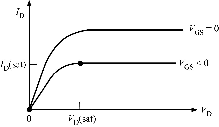
Next, we will investigate the gate bias effect. When the gate-to-channel junction of a MESFET is reverse-biased, the depletion width gets wider, and VD(sat) will decrease.
$$ V_{\text{D}} \left( {\text{sat}} \right) = \frac{{qa^{2} N_{d} }}{2\epsilon } - V_{0} + V_{\text{GS}} $$
(9.5)
Since VGS is negative for reverse bias of the gate–channel junction, VD(sat) is decreased as shown in Fig. 9.3.
../images/325043_1_En_9_Chapter/325043_1_En_9_Fig3_HTML.png
Fig. 9.3

Modification of current–voltage characteristics for VG < 0

The depletion width W eventually will reach across the channel thickness a when the gate reverse bias is further increased. The gate voltage at which the conduction channel is pinched off when VD = 0 is called the threshold voltage VT. For a gate bias of VGS and VD = 0, the depletion width is expressed as
$$ W = \sqrt {\frac{2\epsilon }{{qN_{d} }}\left( {V_{0} - V_{\text{GS}} } \right)} $$
(9.6)
At the threshold voltage VGS = VT, W = a. This leads to
$$ a^{2} = \frac{2\epsilon }{{qN_{d} }}\left( {V_{0} - V_{T} } \right) $$
(9.7)
$$ V_{T} = V_{0} - \frac{{qa^{2} N_{d} }}{2\epsilon } = V_{0} - V_{P} $$
(9.8)
We define VP as the pinch-off voltage, which is the potential across the depletion region at the threshold condition (W = a).
$$ V_{P} = \frac{{qa^{2} N_{d} }}{2\epsilon } $$
(9.9)

The depletion width in a MESFET with VGS = 0 can be either greater than or less than the channel thickness because of the contact potential. If W < a, a channel exists with zero gate bias. The device is operated in the depletion mode. On the other hand, if W > a, the depletion region extends across the channel in equilibrium, and no significant channel current can flow. A positive gate voltage must be applied to reduce the depletion width to a value smaller than the channel thickness a. The device is operated in the enhancement mode.
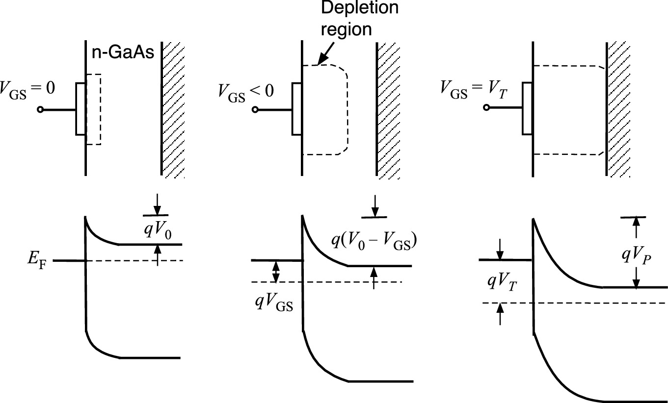
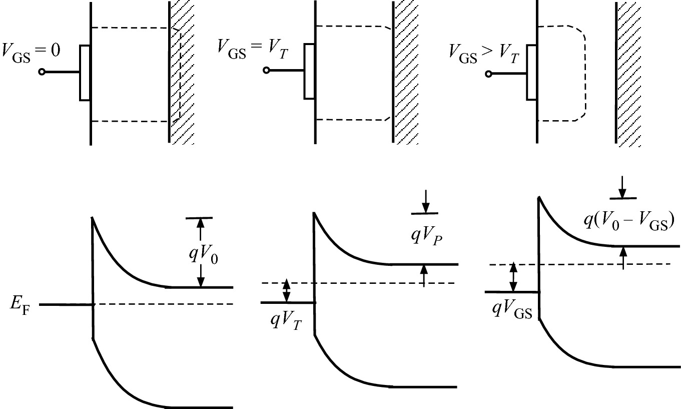
Figure 9.4 shows the energy band diagrams of a depletion-mode MESFET under VD = 0 and various VGS. A reverse bias on the gate (VGS < 0) is required to modulate the channel width. The threshold voltage VT can also be termed the ‘turn-off’ voltage of the device. For enhancement-mode MESFETs, a positive gate bias is required to open the channel. The energy band diagrams for various bias conditions (VD = 0) are shown in Fig. 9.5.
../images/325043_1_En_9_Chapter/325043_1_En_9_Fig4_HTML.png
Fig. 9.4

Depletion region profile under the gate and energy band diagrams of depletion-mode MESFET under VD = 0 and various VGS (negative)
../images/325043_1_En_9_Chapter/325043_1_En_9_Fig5_HTML.png
Fig. 9.5

Depletion region profile under the gate and energy band diagrams of enhancement-mode MESFET under VD = 0 and various VGS (positive)

9.1.2 Current–Voltage Characteristics
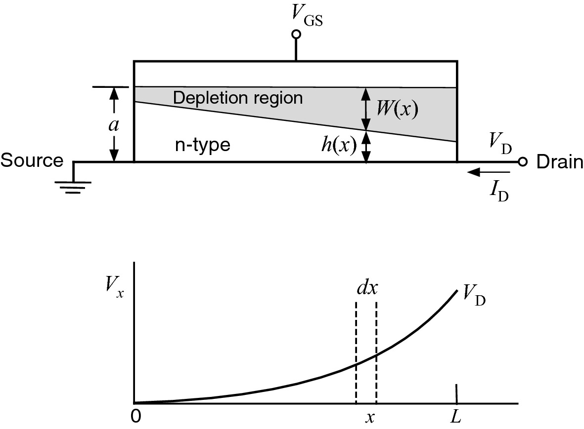
A one-dimensional model is used to develop the DC current–voltage (IV) characteristics of a MESFET. It is assumed that no breakdown will be induced before the channel is pinched off and the device has a doping density of Nd in the channel. Furthermore, the active region of the MESFET has a channel length L, junction width Z, channel depth a, depletion width W(x), and conducting channel width h(x). The origin of the x-axis is located at the edge of the gate adjacent to the source. A schematic of the MESFET structure and the corresponding voltage drop due to the drain bias is shown in Fig. 9.6.
../images/325043_1_En_9_Chapter/325043_1_En_9_Fig6_HTML.png
Fig. 9.6

Schematic diagram of the conducting channel, dimensions, and potential drop along the channel

The current at position x in the channel is described as
$$ I_{\text{D}} \left( x \right) = A\left( x \right)\sigma F\left( x \right) = \frac{Zh\left( x \right)}{\rho }\frac{{{\text{d}}V_{x} }}{{{\text{d}}x}} $$
(9.10)
where σ is the channel conductivity, ρ is the resistivity of the channel material, $$ h(x) = a - W(x) $$, $$ W = \sqrt {\left( {2\epsilon /qN_{d} } \right)\left( {V_{0} - V_{\text{GS}} + V_{x} } \right)} $$ and $$ V_{P} = qa^{2} N_{d} /2\epsilon $$. Since the drain current is a constant and independent of x, we can solve ID by integration.
$$  \begin{aligned}   I_{{\text{D}}} \mathop \int \limits_{0}^{L} {\text{d}}x &amp;  = I_{{\text{D}}} L = \frac{{Za}}{\rho }\mathop \int \limits_{0}^{{V_{0} }} \left[ {1 - \sqrt {\frac{{V_{0}  + V_{x}  - V_{{{\text{GS}}}} }}{{V_{P} }}} } \right]{\text{d}}V_{x}  \\     &amp; \quad  = \frac{{Za}}{\rho }\left[ {V_{x}  - \frac{2}{3}\frac{{\left( {V_{0}  + V_{x}  - V_{{{\text{GS}}}} } \right)^{{3/2}} }}{{\sqrt {V_{P} } }}} \right]_{0}^{{V_{{\text{D}}} }}  \\  \end{aligned}   $$
$$ \therefore \quad I_{\text{D}} = G_{0} V_{P} \left[ {\frac{{V_{\text{D}} }}{{V_{P} }} - \frac{2}{3}\left( {\frac{{V_{0} + V_{\text{D}} - V_{\text{GS}} }}{{V_{P} }}} \right)^{3/2} + \frac{2}{3}\left( {\frac{{V_{0} - V_{\text{GS}} }}{{V_{P} }}} \right)^{3/2} } \right] $$
(9.11)
where G0 is the channel conductance at W(x) = 0 and G0 ≡ Za/ρL. This is the complete IV characteristic equation for all bias conditions.
In the low bias region, where VD ≪ V0VGS, the IV characteristics have a linear relationship. We can first rewrite ID in the following form:
$$ I_{\text{D}} = G_{0} \left\{ {V_{\text{D}} - \frac{2}{{3\sqrt {V_{P} } }}\left( {V_{0} - V_{\text{GS}} } \right)^{3/2} \left[ {\left( {1 + \frac{{V_{\text{D}} }}{{V_{0} - V_{\text{GS}} }}} \right)^{3/2} - 1} \right]} \right\} $$
(9.12)
Then, using Taylor series expansion of $$ \left( {1 + x} \right)^{n} \cong \left( {1 + nx} \right) $$ for x ≪1, we have
$$  \begin{aligned}   I_{{\text{D}}}  &amp;  \approx G_{0} \left\{ {V_{{\text{D}}}  - \frac{2}{{3\sqrt {V_{P} } }}\left( {V_{0}  - V_{{{\text{GS}}}} } \right)^{{3/2}} \left[ {\left( {1 + \frac{{3V_{{\text{D}}} /2}}{{V_{0}  - V_{{{\text{GS}}}} }}} \right) - 1} \right]} \right\} \\     &amp; \quad  = G_{0} V_{{\text{D}}} \left[ {1 - \frac{{\sqrt {V_{0}  - V_{{{\text{GS}}}} } }}{\sqrt{{V_{P}} }}} \right] \propto V_{{\text{D}}}  \\  \end{aligned}   $$
(9.13)

The drain current simply increases linearly with drain bias voltage.

At the other end of the spectrum, the conduction current saturates at high drain bias when the channel is pinched off. The IV relationship described above is only valid up to pinch-off, where $$ V_{P} = V_{\text{D}} \left( {\text{sat}} \right) + V_{0} - V_{\text{GS}} $$. Using this pinch-off voltage relation in (9.11), the saturation current is obtained as
$$ I_{\text{D}} \left( {\text{sat}} \right) = G_{0} V_{P} \left[ {\frac{{V_{\text{D}} \left( {\text{sat}} \right)}}{{V_{P} }} - \frac{2}{3} + \frac{2}{3}\left( {\frac{{V_{0} - V_{\text{GS}} }}{{V_{P} }}} \right)^{3/2} } \right] $$
(9.14)
This equation can be further reduced by replacing $$ V_{\text{D}} ({\text{sat}}) /V_{P} $$ with $$ 1 - \left( {V_{0} - V_{\text{GS}} } \right)/V_{P} $$.
$$ I_{\text{D}} \left( {\text{sat}} \right) = G_{0} V_{P} \left[ {\frac{1}{3} - \left( {\frac{{V_{0} - V_{\text{GS}} }}{{V_{P} }}} \right) + \frac{2}{3}\left( {\frac{{V_{0} - V_{\text{GS}} }}{{V_{P} }}} \right)^{3/2} } \right] $$
(9.15)
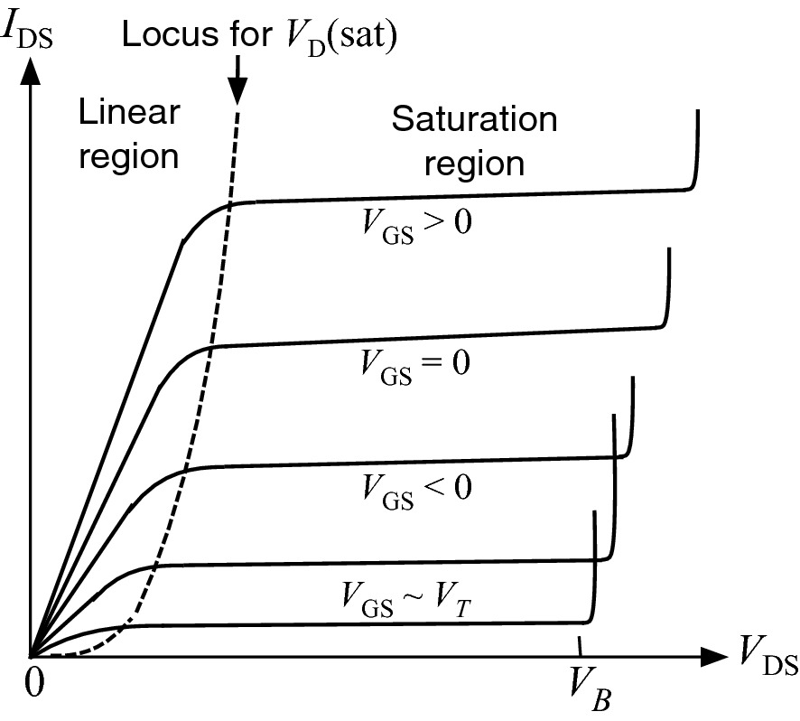
The typical IV characteristics of an n-channel depletion-mode MESFET are shown in Fig. 9.7. The drain current flows for VGS are less negative than the threshold voltage VT. At sufficiently high drain bias, VB, avalanche breakdown occurs between the gate and drain and the drain current increases abruptly.
../images/325043_1_En_9_Chapter/325043_1_En_9_Fig7_HTML.png
Fig. 9.7

Typical current–voltage characteristics of a depletion-mode MESFET. Breakdowns occur at the breakdown voltages VB

9.1.3 Transconductance and Equivalent Circuit of MESFET

One of the figures of merit of the MESFET is the transconductance, gm, which describes the effect of the input voltage change on the output current. In the equivalent circuit model, the intrinsic transconductance gmi times the input voltage represents a current source. Under a fixed drain bias, the change in gate voltage leads to a depletion layer width change. Because the space charge in the depletion region changes by ΔQG in a time interval of τ, a drain current change is induced.
$$ \Delta I_{\text{DS}} = \frac{{\Delta Q_{\text{G}} }}{\tau }\quad {\text{or }}\quad     \left. {\frac{{\partial I_{\text{DS}} }}{{\partial Q_{\text{G}} }}} \right|_{{V_{\text{DS}} }} = \frac{1}{\tau } $$
(9.16)
The rate of conduction current change with respect to the charge change in the depletion region defines a carrier transient time (τ) crossing the conduction channel. The intrinsic transconductance, gmi, is then defined as
$$ {\text{g}}_{mi} \equiv \left. {\frac{{\partial I_{\text{DS}} }}{{\partial V_{\text{GS}} }}} \right|_{{V_{\text{DS}} }} = \left. {\frac{{\partial I_{\text{DS}} }}{{\partial Q_{\text{G}} }}} \right|_{{V_{\text{DS}} }} \cdot \left. {\frac{{\partial Q_{\text{G}} }}{{\partial V_{\text{GS}} }}} \right|_{{V_{\text{DS}} }} = \frac{{C_{\text{G}} }}{\tau } $$
(9.17)

CG is the total gate capacitance and CG = CGS + CDG, where CGS and CDG are the gate-to-source capacitance and drain-to-gate capacitance, respectively. To increase gmi, we have to reduce τ. The minimization of τ can be achieved either by using materials with high drift velocity or by minimizing the channel length through the reduction of gate length. The approach of increasing the total gate capacitance to achieve high gmi is not practical, since it will limit the frequency response of the device.

Next, we examine the property of the drain terminal. For a fixed gate bias, a change in VDS will also change the space charge in the depletion region, ΔQG, which defines a current change, ΔIDS, and leads to a drain-to-gate capacitance CDG.
$$ C_{\text{DG}} \equiv \left. {\frac{{\partial Q_{\text{G}} }}{{\partial V_{\text{DS}} }}} \right|_{{V_{\text{GS}} }} $$
(9.18)
The current–voltage change further defines a drain-to-source output conductance (Go):
$$ G_{\text{o}} \equiv \left. {\frac{{\partial I_{\text{DS}} }}{{\partial V_{\text{DS}} }}} \right|_{{V_{\text{GS}} }} = \left. {\frac{{\partial I_{\text{DS}} }}{\partial Q}} \right|_{{V_{\text{GS}} }} \cdot \left. {\frac{\partial Q}{{\partial V_{\text{DS}} }}} \right|_{{V_{\text{GS}} }} $$
(9.19)
where Q is the total charge in conduction channel.
Assuming the carrier velocity υ is constant in the conduction channel of an effective length Leff, ΔIDS ~ ΔQt, and Δt ~ Leff/υ, the right-hand side of the output conductance (9.19) can be expressed as
$$ \left. {\frac{{\partial I_{\text{DS}} }}{\partial Q}} \right|_{{V_{\text{GS}} }} \cong \frac{\upsilon }{{L_{\text{eff}} }}\quad {\text{and}}\quad \left. {\frac{\partial Q}{{\partial V_{\text{DS}} }}} \right|_{{V_{\text{GS}} }} \equiv C_{\text{o}} $$
(9.20)
Co defines an output capacitance.
$$ \therefore \;G_{\text{o}} = \frac{{C_{\text{o}} \upsilon }}{{L_{\text{eff}} }} $$
(9.21)

To achieve large Go, high carrier mobility and small gate length are necessary.
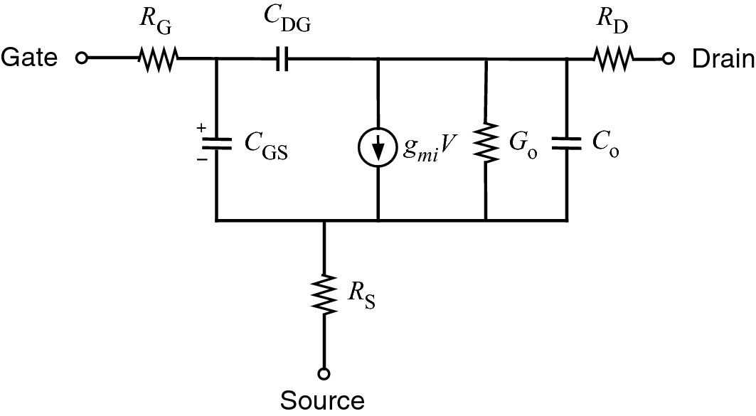
Figure 9.8 shows a simple intrinsic equivalent circuit model of the MESFET that ignores all parasitic elements except the terminal series resistances RG, RS, and RD.
../images/325043_1_En_9_Chapter/325043_1_En_9_Fig8_HTML.png
Fig. 9.8

Intrinsic equivalent circuit model of the MESFET including terminal series resistances

9.1.4 High-Speed Figure of Merit
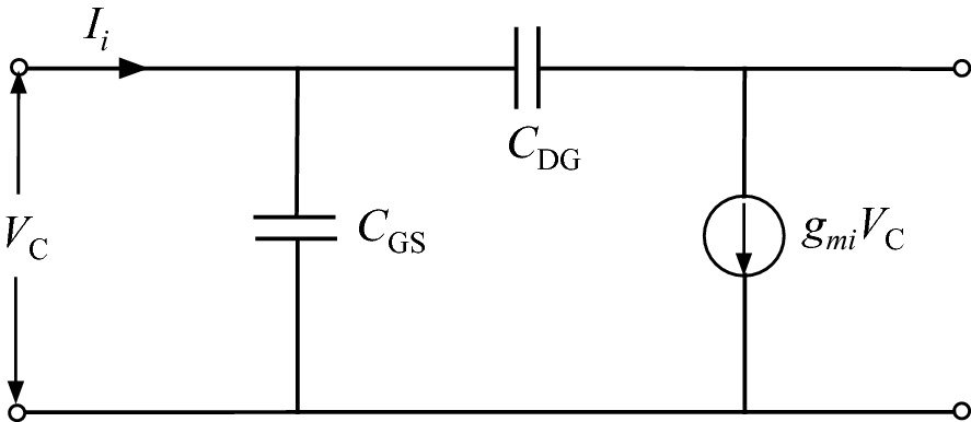
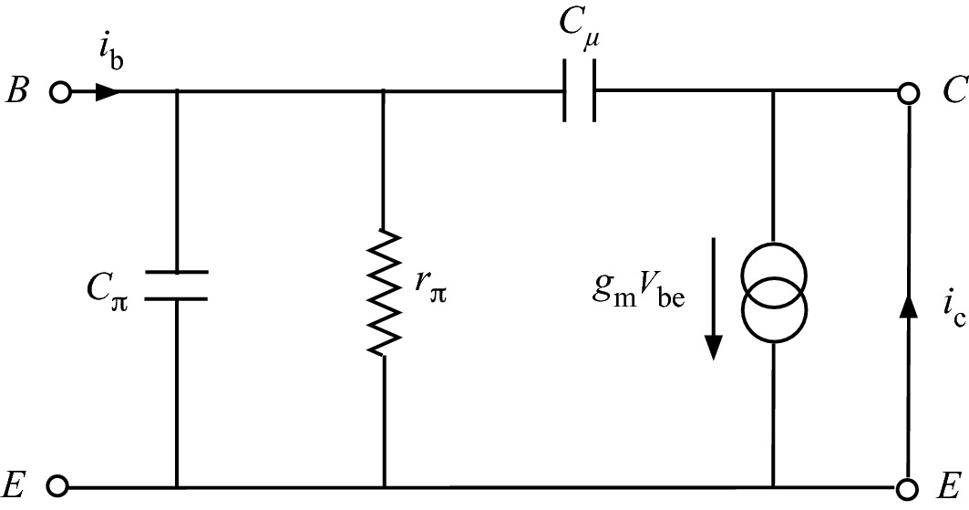
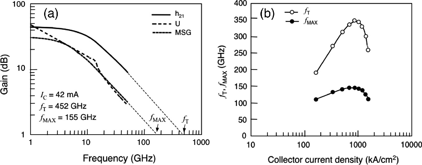
The high-frequency performance of a MESFET is usually characterized by parameters related to its ultimate operation frequency. However, these parameters are difficult to measure due to the fact that the performance of the device under testing can depend as much on the measurement circuit as on the device itself. As a result, high-frequency transistors are commonly characterized by frequency-dependent gains, deduced from network-analyzer measurements. The high-frequency performance of the device measured in this way is reasonably independent of the circuit in which it is placed. There are two gains commonly used to deduce the small signal, linear-operation figure of merit of the device. One of these gains is h21, which is the forward current gain with the output short-circuited. The frequency at which this gain extrapolates to one is the unity short-circuit current gain frequency fT. Consider the simple intrinsic equivalent circuit of Fig. 9.9. This frequency can be derived as the frequency at which the magnitude of the input current Ii equals the magnitude of the ideal output current gmiVC of the transistor. When the output is short-circuited,
../images/325043_1_En_9_Chapter/325043_1_En_9_Fig9_HTML.png
Fig. 9.9

Intrinsic equivalent circuit of a MESFET for frequency response analysis

$$ \left| {I_{i} } \right| = \left| {i\omega \left( {C_{\text{GS}} + C_{\text{DG}} } \right)V_{\text{C}} } \right| = 2\pi f_{\text{T}} \left( {C_{\text{GS}} + C_{\text{DG}} } \right)V_{\text{C}} = {\text{g}}_{mi} V_{\text{C}} $$
(9.22)
$$ f_{\text{T}} = \frac{1}{2\pi }\left( {\frac{{{\text{g}}_{mi} }}{{C_{\text{GS}} + C_{\text{DG}} }}} \right) = \frac{{{\text{g}}_{mi} }}{{2\pi C_{\text{G}} }} = \frac{1}{2\pi \tau } $$
(9.23)

This equation shows that fT is a measure of a quantity that is fundamental to the device—the delay time of the current through the conduction channel.

The other important figure of merit of the transistor is the maximum frequency of oscillation, fmax. At this frequency, the unilateral power gain (U) of the device becomes unity. It is the highest frequency at which the transistor can amplify the power of a signal and can be expressed as
$$ f_{{\max} } \approx \frac{{f_{\text{T}} }}{{2\sqrt {G_{\text{o}} \left( {R_{\text{G}} + R_{\text{S}} } \right) + 2\pi f_{\text{T}} C_{\text{DG}} R_{\text{G}} } }} $$
(9.24)

The fmax of a MESFET may be either above or below its fT, depending on the specific circuit values in the above equation.

9.1.5 MESFET Fabrication and Performance
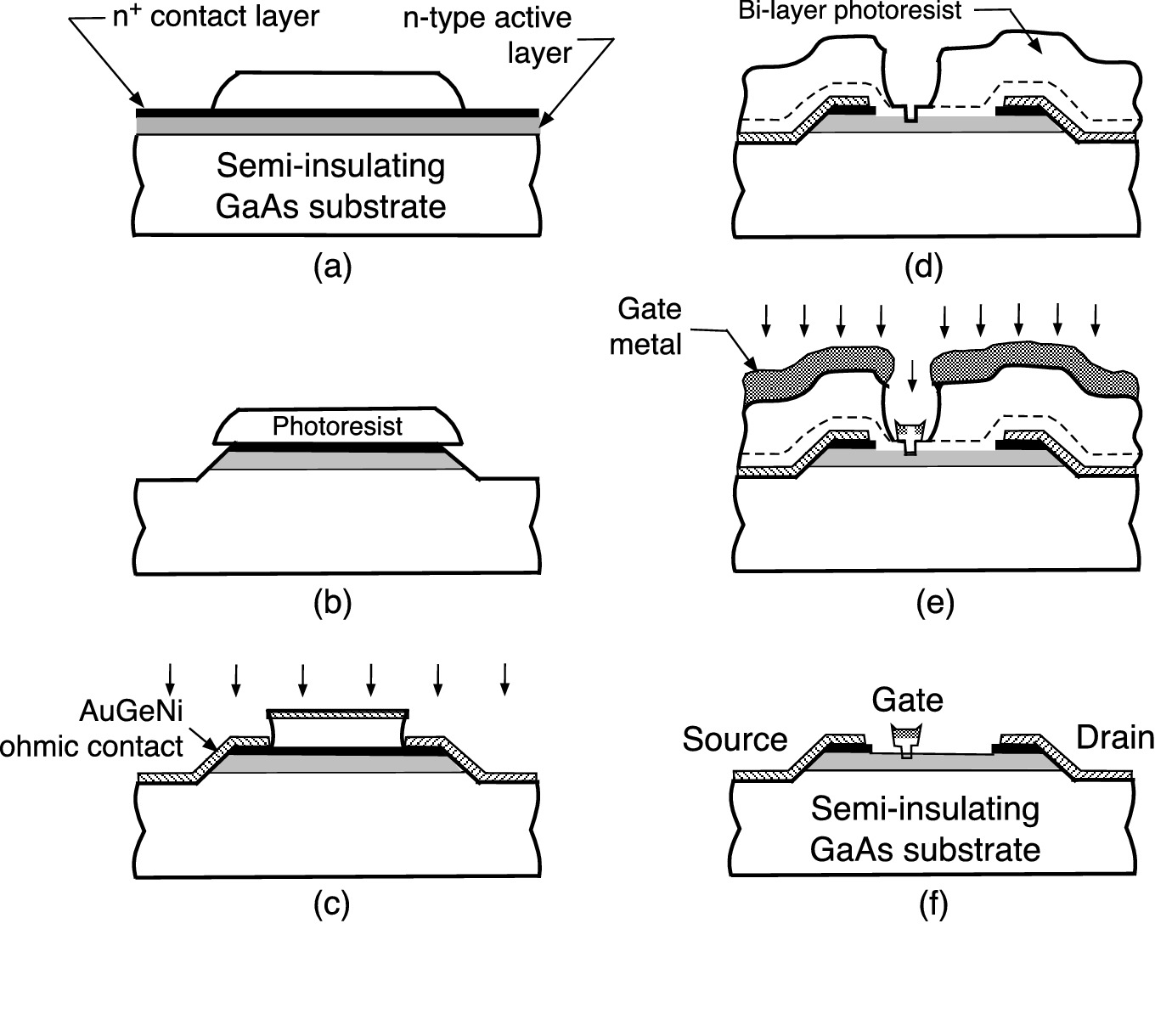
A typical fabrication sequence for a high-speed MESFET is shown in Fig. 9.10. The process was designed to maximize the cutoff frequency of the transistor by minimizing the contact resistances, reducing the parasitic in the active conduction channel, and shortening the gate length. An n+ contact layer is added on top of the conduction channel layer outside the gate region to reduce the source and drain contact resistances RS and RD. In addition, a thick channel layer outside the gate area is used to minimize the surface depletion-induced additional resistance. To maintain a short gate length while minimizing the gate contact resistance RG, the usual practice is to use a ‘T’ gate design where a thick top metal contact with a narrow base is adopted. The gate is situated in a recess of the channel layer in order to control the threshold voltage, VT. The gate recess is usually off-centered and located near the source contact to minimize RS. The gate–drain separation, LGD, is designed to be greater than the depletion width at the breakdown voltage.
../images/325043_1_En_9_Chapter/325043_1_En_9_Fig10_HTML.png
Fig. 9.10

Typical fabrication sequence of submicron GaAs MESFET using the double-recess process. a Epitaxy and using photoresist (PR) to define device active area, b mesa etch for isolation, c source and drain ohmic contacts deposition, d channel recess etch and gate recess etch using bilayer PR process, e T-gate metal deposition, and f PR liftoff to complete MESFET process
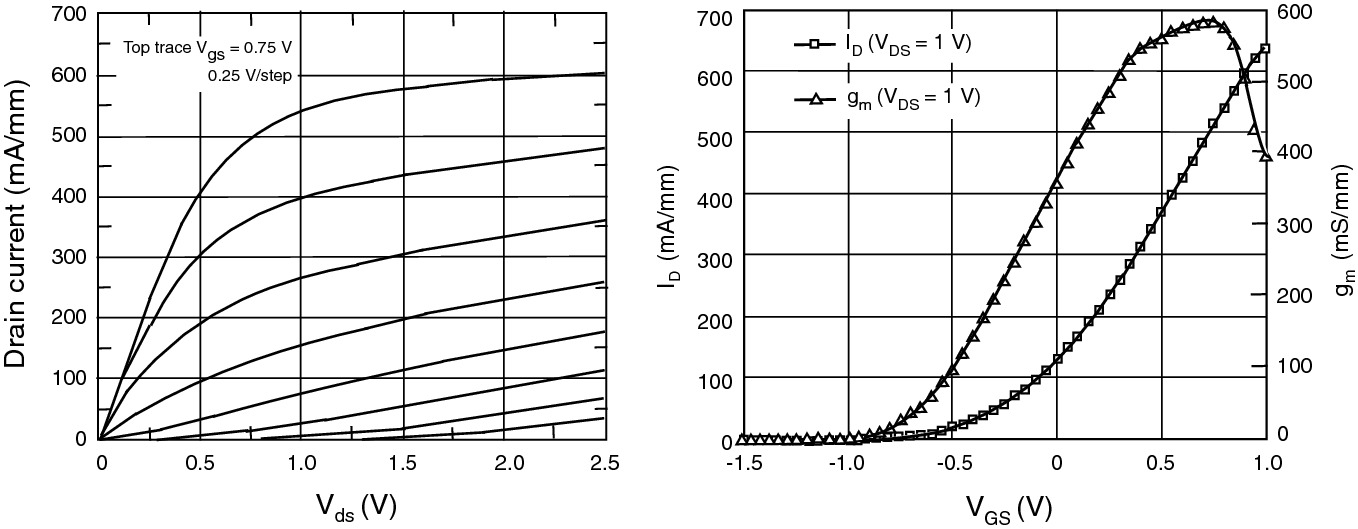
The fabricated MESFETs are characterized by measuring their I–V characteristics, gm, fT, and fmax. Figure 9.11 shows the IV characteristics of a 0.12 × 50 µm2 dual-gate GaAs depletion-mode MESFET. The drain currents show weak saturation for the negative gate bias voltages. This is a common behavior called short-channel effect in MESFETs with gate length less than 0.25 µm.
../images/325043_1_En_9_Chapter/325043_1_En_9_Fig11_HTML.png
Fig. 9.11

Measured ID-VDS characteristics and channel current and transconductance versus gate bias of a dual-gate (0.12 µm × 50 µm) GaAs MESFET.

Courtesy M. Feng, University of Illinois at Urbana-Champaign

The short-channel effect is due to the less efficient inter-valley transfer of electrons from the Γ-valley to the L-valley at high fields in short-channel devices. Thus, most electrons stay in the Γ-valley when reaching the drain and show as a weaker velocity saturation. The parasitic leakage through the semi-insulating substrate also contributes to the lack of current saturation for the more negative gate-voltage region. The transconductance gm is deduced from the drain current variation under various gate bias voltages. Note that the measured gm is the extrinsic transconductance including the effect of RS and expressed as
$$ {\text{g}}_{m} = \frac{{{\text{g}}_{mi} }}{{1 + {\text{g}}_{mi} R_{\text{S}} }} $$
(9.25)
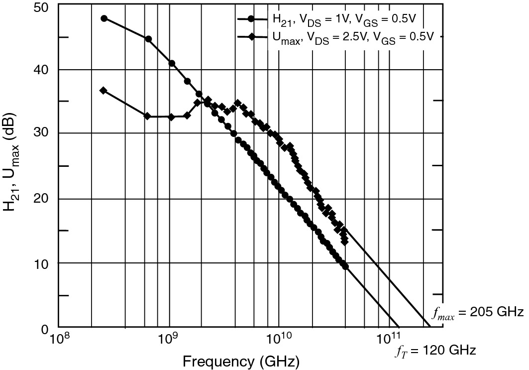
The maxima fT and fmax of the MESFET are estimated to be 110 and 235 GHz, respectively, and shown in Fig. 9.12. These values are deduced from the measured low-frequency values of h21 and Umax up to 40 GHz using a roll-off of −6 dB/octave.
../images/325043_1_En_9_Chapter/325043_1_En_9_Fig12_HTML.png
Fig. 9.12

Measured unity current gain frequency fT (H21) and maximum cutoff frequency fmax of the same dual-gate (0.12 µm × 50 µm) GaAs MESFET characterized in Fig. 9.11.

Courtesy M. Feng, University of Illinois at Urbana-Champaign
9.2 Modulation Doping and Two-Dimensional Electron Gas (2DEG)

As shown in Fig. 4.​7, the carrier mobility of a semiconductor is determined by the sum of inverse mobility components (µi) due to different scattering mechanisms, i.e., µ−1 = Σ(µi)−1. At a fixed temperature, the lowest mobility component dominates the total carrier mobility. In binary compound semiconductor alloys, the major scattering processes are the optical phonon (polar) scattering at high temperature, the ionized impurity scattering at low temperature, the acoustic phonon scattering due to piezoelectric field, and the acoustic phonon scattering due to deformation potential. With the exception of the impurity scattering, the effect of all scattering mechanisms on electron mobility can be reduced at low temperatures. The total temperature-dependent electron mobility increases with decreasing temperature and reaches a maximum value before decreasing with further reducing temperature. One way to reduce the ionized impurity scattering at low temperature is to use high-purity materials, as evidenced in Fig. 4.​7, where there are fewer ionized impurities. However, for most high-speed device applications, certain doping concentrations have to be maintained. Therefore, this option is not practical. In 1978, R. Dingle and colleagues at Bell Laboratories invented a modulation-doping technique to eliminate the influence of ionized impurity scattering in heterojunction superlattices [1]. By separating the physical location of ionized dopants from generated electrons across the heterojunction, with ionized impurities on the large bandgap semiconductor side and generated conduction electrons on the undoped small bandgap semiconductor side, electron mobility much higher than the equivalent bulk material was achieved at low temperature without sacrificing the carrier concentration. Since these conduction electrons occupy a thin layer (≤100 Å) in the triangular quantum well formed at the heterojunction interface, they can only move easily close to and parallel to the heterojunction interface. These electrons form an electron cloud, or a pseudo-two-dimensional electron gas (2DEG), in the modulation-doped heterostructure. Based on this concept, a new type of FET, the high-electron-mobility transistor (HEMT), was derived.

9.2.1 Modulation-Doped (MD) Heterostructures
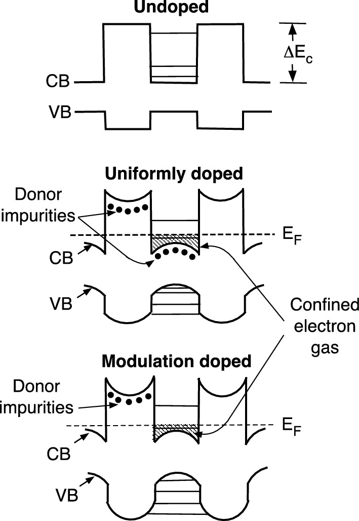
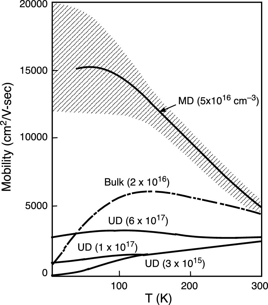
The modulation-doping concept was first developed utilizing heterojunction superlattices as shown in Fig. 9.13. In a superlattice structure with type-I band alignment, quantum wells are formed in both conduction and valence bands. Under equilibrium conditions, a continuous Fermi level throughout the superlattice causes appreciable band bending, leading to the formation of pseudotriangular quantum wells at heterojunctions. When the superlattice is either uniformly doped (UD) or modulation-doped (MD) with donor impurities, due to the high potential energy associated with the barrier layer relative to the quantum well, electrons associated with donor impurities in barriers will move into quantum wells. In both UD and MD superlattice structures, the carriers confined to the pseudotriangular quantum well form a 2DEG. The ionized impurity scattering in the conduction channel is removed in MD structures, where 2DEG conduction electrons and their parent donor impurities are spatially separated from each other in an irreversible manner. The electron mobility of the 2DEG suffers no ionized impurity scattering, leading to a much higher mobility, especially at low temperatures. Figure 9.14 shows the temperature-dependent electron mobility of bulk, UD and MD GaAs structures. The UD and MD structures used the AlGaAs/GaAs material system. The electron mobility enhancement at low temperatures clearly demonstrates the reduction (or even a lack) of impurity scattering as expected. Since the doped barrier layers are totally depleted in MD superlattice structures, the electron density in the quantum well may greatly exceed the unintentionally doped impurity density. Thus, the concentration of 2DEG is independent of the doping level in the conduction channel. By the same token, an enhanced hole mobility of the two-dimensional hole gas (2DHG) is achievable in p-type MD heterostructures.
../images/325043_1_En_9_Chapter/325043_1_En_9_Fig13_HTML.png
Fig. 9.13

Energy band diagrams for n-doped and undoped GaAs-AlxGa1−xAs superlattices.

Reprinted with permission from [1], copyright AIP Publishing
../images/325043_1_En_9_Chapter/325043_1_En_9_Fig14_HTML.png
Fig. 9.14

Temperature-dependent electron mobility for bulk GaAs and several undoped UD and MD superlattices. The cross-hatched region includes most of the MD data.

Reprinted with permission from [1], copyright AIP Publishing
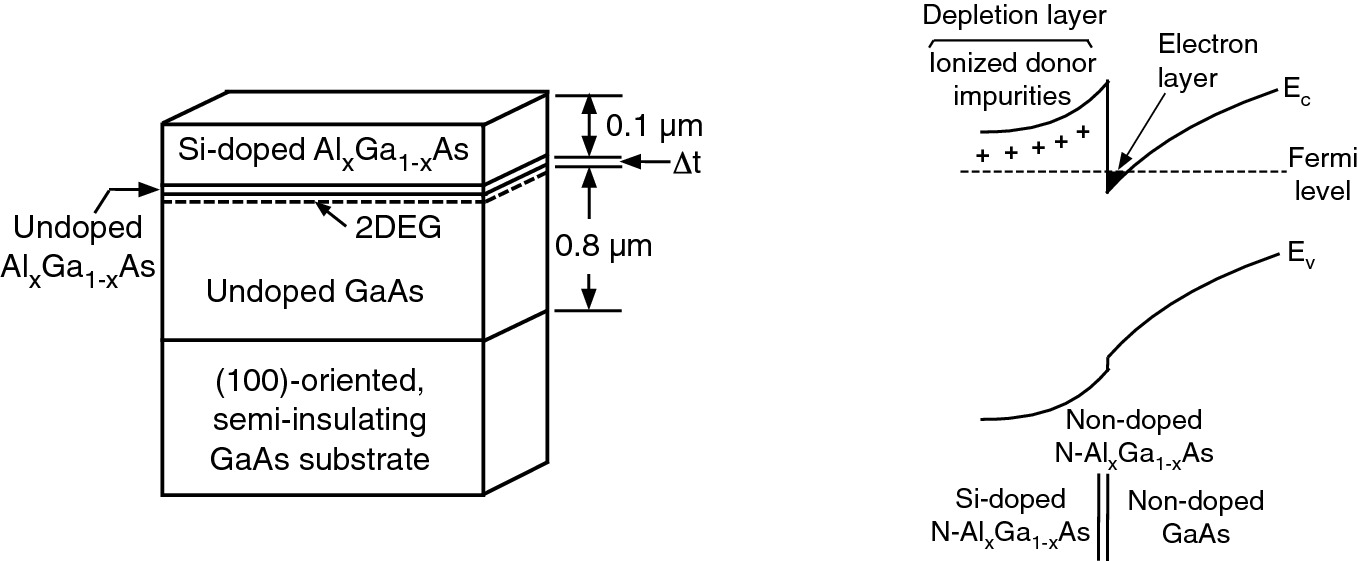
Of course, a superlattice heterostructure with multiple MD heterojunctions is not necessary for device implementation. With a proper energy band discontinuity, a single MD heterojunction is sufficient to form a 2DEG at the heterostructure interface and to achieve the electron mobility enhancement. In fact, for FET applications, the single MD heterojunction design makes it easy to control the channel charge carriers. The first FET utilizing the high-electron-mobility feature of the MD heterostructure has just one hetero-interface as shown in Fig. 9.15. This design first demonstrated by engineers at Fujitsu Laboratories in Japan—a high-electron-mobility transistor (HEMT) design, as it was called—became the standard structure of future FETs utilizing 2DEG in the conduction channel [2].
../images/325043_1_En_9_Chapter/325043_1_En_9_Fig15_HTML.png
Fig. 9.15

Layer structure and energy band diagram of an MD GaAs-AlxGa1−xAs heterostructure grown by MBE with a spacer layer inserted between the barrier layer and the 2DEG channel.

Reprinted with permission from [2, 3], copyright Japanese Society of Physics

9.2.2 Scattering Mechanisms in MD Heterostructures

It is important to analyze various scattering mechanisms limiting the mobility in the 2DEG in order to be able to provide interface design rules for yielding high-performance devices. In addition to the bulk scattering mechanisms, some additional scattering mechanisms unique to heterojunctions are introduced here. A GaAs/AlGaAs MD heterostructure similar to the HEMT structure shown in Fig. 9.15 is used to illustrate the properties of added scattering mechanisms. On the semi-insulating GaAs substrate, an undoped GaAs channel layer was first grown, followed by a silicon-doped n-type AlGaAs barrier layer to complete the MD heterostructure. The 2DEG channel will be formed at the GaAs/AlGaAs interface just inside the undoped GaAs layer.

  1. (a)

    Coulomb interaction from ionized impurities located in the barrier


Since the 2DEG is located right next to the hetero-interface, the physical quality of the interface as well as any force exerted that diverts the transport direction toward the interface will affect the nature of carrier scattering. The attraction force due to Coulomb interaction between 2DEG in the conduction channel and its ionized parent donor impurities in the barrier layer will cause electrons to scatter with the hetero-interface. The electron mobility is reduced due to this added scattering mechanism. The carrier mobility is thus a function of the 2DEG sheet charge density. At a low barrier doping density (small 2DEG sheet charge density), the Coulomb interaction is weak and the electron mobility is limited by the background scattering in the undoped GaAs channel. For a heavily doped barrier layer structure, the Coulomb interaction dominates the carrier scattering process.

The Coulomb scattering problem cannot be totally eliminated but can be reduced by setting back the doping region of the barrier layer away from the hetero-interface. This undoped barrier layer inserted between the 2DEG and doped barrier layer is called a spacer layer [4]. Remember, the Coulomb attraction force is inversely proportional to the square of the charge separation distance. For a fixed doping density in the barrier, the Coulomb interaction between the 2DEG and ionized donors weakens with increasing spacer layer thickness, thus increasing electron mobility. However, due to the decreased electron transfer rate from the thicker barrier layer to the conduction channel, for a fixed barrier doping density, the sheet density of the 2DEG will decrease with increasing spacer layer thickness. In practical devices, a compromised spacer layer thickness of 25–30 Å is used to optimize the electron mobility while maintaining a high 2DEG sheet charge density.

  1. (b)

    Interface-roughness-induced scattering
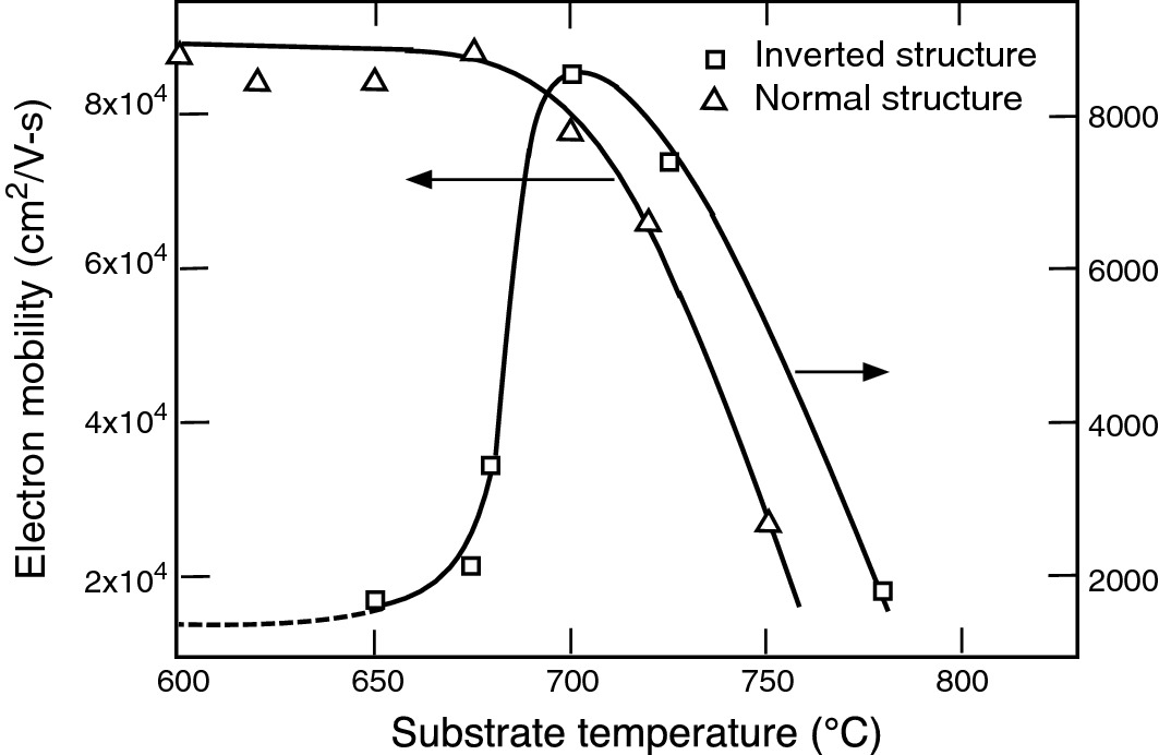
     
Since the 2DEG in the conduction channel of an MD heterostructure is located very close to the hetero-interface, any minute interface roughness could induce additional scattering and decrease the carrier mobility. Normally, in MD heterostructures, the AlGaAs barrier layer is grown on top of the GaAs 2DEG channel layer using MBE. The surface morphology of the GaAs channel layer at the hetero-interface is critically important. An extremely flat and smooth GaAs/AlGaAs interface is usually achieved under proper growth conditions including a wide range of V/III flux ratio, substrate temperature, and growth rate. This layer structure is convenient for FET-like device fabrication, including HEMT, and is called the normal MD heterostructure. If the layer sequence is reversed such that the GaAs 2DEG channel layer is placed on top of the AlGaAs barrier layer, the structure is called an inverted MD heterostructure. To achieve high electron mobility in such structures, an extremely smooth AlGaAs surface morphology is required. However, only under a very narrow MBE growth window does the AlGaAs show a less rough surface. Figure 9.16 shows the difference in the 77 K electron mobility for normal and inverted MD heterostructures grown at various substrate temperatures with a 75 Å spacer layer. The 2DEG mobilities for normal and inverted MD structures are shown at different scales in the figure. Note that, even using the optimal AlGaAs growth temperature, the electron mobility of the inverted structure is still an order of magnitude smaller than that of the normal structure.
../images/325043_1_En_9_Chapter/325043_1_En_9_Fig16_HTML.png
Fig. 9.16

Measured 2DEG mobility of normal and inverted MD GaAs/AlGaAs heterostructures grown at different temperatures.

Reprinted with permission from [4], copyright AIP Publishing

  1. (c)

    Inter-subband scattering at high carrier density


Since the 2DEG is confined in the quasi-triangular QW at the hetero-interface, electrons are occupying the quantized states of the QW. The ground state gets populated first with electrons transferred from the barrier layer. When the ground state is fully populated, any further increase of the transferred electron density will have to occupy the higher energy states. The scattering probability is increased for the multiple-state system, and it reduces the total electron mobility.
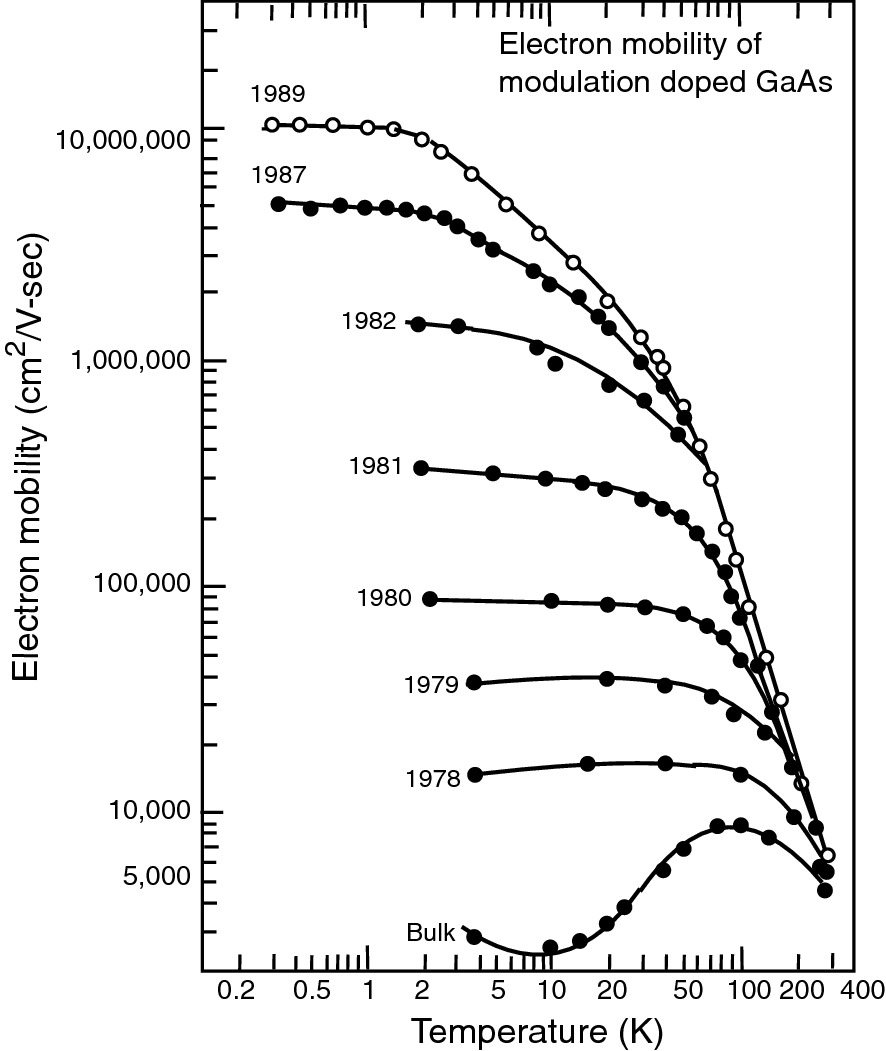
The electron mobility values of the modulation-doped heterostructures have progressed steadily since 1978 (Fig. 9.17). In just three years, low-temperature electron mobility of over one million (cm2/V s) was achieved in many laboratories. Further improvements of MD heterostructure designs and growth techniques pushed the electron mobility of the 2DEG over the 10 million (cm2/V s) mark in 1989 at Bell Laboratories. A very thick spacer layer (70 Å) and planar (delta) doping scheme were used to minimize the Coulomb-interaction-induced interface scattering. The superlattice buffer layer beneath the GaAs channel was extensively used to guarantee minimized interface roughness scattering. Furthermore, to minimize the background doping concentration in the GaAs channel layer, the MBE system was thoroughly baked at high temperature (>200 °C) to get rid of volatile impurities inside and kept under liquid nitrogen cooling all the time. These grown samples provided a wonderful playground for some solid-state physicists, but have no immediate device application due to the low 2DEG sheet charge density achieved.
../images/325043_1_En_9_Chapter/325043_1_En_9_Fig17_HTML.png
Fig. 9.17

Progress of peak mobility achieved in 2DEG as a function of temperature over a span of 12 years

Reprinted with permission from [5], copyright AIP Publishing

9.3 High-Electron-Mobility Transistor Basics—A Triangular Quantum Well Approach

The FET structure based on a 2DEG in the conduction channel was first demonstrated in 1980 by Fujitsu Laboratory of Japan, less than two years after the inception of the MD concept at Bell Laboratories. Therefore, there were different names used for this newly developed FET. The Fujitsu group called it the HEMT (high-electron-mobility transistor), Bell Laboratories named it SDHT (selectively-doped hetero-field-effect transistor), and the group at Thomson CSF in France called it TEGFET (two-dimensional electron gas field-effect transistor). The name MODFET (modulation-doped field-effect transistor) has also been used. Today, HEMT is the most commonly used name for this kind of FET.

The basic device structure of the HEMT is very similar to a MESFET, as shown in Fig. 9.18. Similar to a MESFET, the conduction current flows between the source and drain, and the amount of current flow is controlled by the gate bias. However, a HEMT does not use the gate bias to adjust the width of the conduction channel. Rather, the gate bias modulates the Fermi level position and, thus, controls the 2DEG sheet carrier density in the conduction channel. In this section, we will use a simple pseudotriangular QW approach to examine the equilibrium 2DEG sheet carrier density of a heterostructure.
../images/325043_1_En_9_Chapter/325043_1_En_9_Fig18_HTML.png
Fig. 9.18

Schematic structure of a GaAs/AlGaAs high-electron-mobility transistor

An ideal triangular QW structure has an infinitely high vertical barrier on one side and a constant slope on the other side. The eigenenergy solutions of the ideal triangular QW are in the form of the Airy functions. If an ideal triangular QW was assumed for the HEMT structure, electrons transferred from the barrier layer fill the first allowed state (E0) in the QW up to the Fermi level (EF). Under ideal conditions, carriers of the 2DEG are solely transferred from the doped barrier layer with a doping concentration Nd and a depletion layer thickness Wd. Thus, the sheet carrier concentration of the 2DEG, NS, simply equals to NdWd (cm−2). However, one should notice that the conduction band structure of the HEMT is far from ideal—the pseudotriangular QW has a finite band discontinuity, ΔEc, on one side and a sublinear energy barrier on the channel side as shown in Fig. 9.19 for an AlGaAs/GaAs HEMT.
../images/325043_1_En_9_Chapter/325043_1_En_9_Fig19_HTML.png
Fig. 9.19

Heterojunction energy band diagram of the HEMT structure shown in Fig. 9.18. The spacer layer in AlGaAs is removed from the heterojunction interface

Using an ideal triangular QW model, the possible sheet charge density (NS) is estimated first. From Gauss’ law for an ideal triangular QW, the displacement flux density (D) relates the sheet charge density and the electric field intensity (F) by
$$ D = \epsilon F = \rho_{S} = qN_{S} \quad {\text{or}}\quad F = qN_{S} /\epsilon $$
(9.26)
Therefore, the ground state inside the QW, E0, can be expressed in terms of NS by
$$ E_{0} = \left( {\frac{{\hbar^{2} }}{{2m^{*} }}} \right)^{1/3} \left( {\frac{{9\pi q^{2} N_{S} }}{8\epsilon }} \right)^{2/3} \approx \gamma N_{S}^{2/3} $$
(9.27)
At T = 0 K, where f(E) = 1, the equilibrium sheet carrier density is given by
$$ N_{S} \approx \mathop \int \limits_{{E_{0} }}^{{E_{\text{F}} }} D_{{ 2 {\text{D}}}} \left( E \right)f\left( E \right){\text{d}}E = \frac{{m^{*} }}{{\pi \hbar^{2} }}\left( {E_{\text{F}} - E_{0} } \right) $$
(9.28)
At a finite temperature,
$$  \begin{aligned}   N_{S}  &amp;  \approx \mathop \int \limits_{{E_{0} }}^{{E_{F} }} D_{{2D}} \left( E \right)\frac{1}{{1 + \exp \left[ {\left( {E_{0}  - E_{F} } \right){\it{/kT}}} \right]}}{\text{d}}E \\     &amp; \quad  = \frac{{m^{*} }}{{\pi \hbar ^{2} }}{kT}\ln \left\{ {1 + \exp \left[ {\left( {E_{F}  - E_{0} } \right){/kT}} \right]} \right\} \\  \end{aligned}  $$
(9.29)
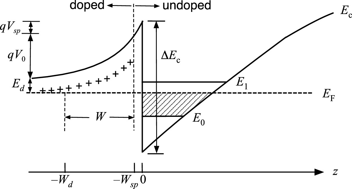
If we include a thin undoped spacer layer with a thickness of Wsp at the interface, a voltage drop Vsp will appear across this layer. According to the energy band diagram shown in Fig. 9.20, the conduction band discontinuity ΔEc at 0 K can be expressed as the following:
../images/325043_1_En_9_Chapter/325043_1_En_9_Fig20_HTML.png
Fig. 9.20

Heterojunction energy band diagram of the HEMT structure shown in Fig. 9.18. The spacer layer in AlGaAs at the heterojunction interface is included

$$ \Delta E_{\text{c}} = qV_{0} + qV_{sp} + E_{d} + E_{0} + \delta E $$
(9.30)
where
$$ \left\{ {\begin{array}{*{20}l} {\delta E = E_{\text{F}} - E_{0} = \displaystyle{\frac{{\pi \hbar^{2} }}{{m^{*}} }}N_{S} } \hfill \\ {V_{0} = \displaystyle{\frac{{qN_{d} W_{d}^{2} }}{2\epsilon }} = \frac{{qN_{S} W_{d} }}{2\epsilon }} \hfill \\ {V_{sp} = \displaystyle{\frac{{qN_{S} W_{sp} }}{\epsilon }}} \hfill \\ \end{array} } \right. $$
(9.31)
Here the bottom tip of the triangular QW is set as E = 0. We notice that each term, except Ed, in this equation is a function of NS and has a unique solution for each EF. By moving the Ed term to the left of the equation, the right-hand side of the equation can be expressed in terms of NS.
$$ \Delta E_{c} - E_{d} = qV_{0} + qV_{sp} + E_{0} + \frac{{\pi \hbar^{2} }}{{m^{*} }}N_{S} $$
(9.32)
$$ \begin{aligned}\Delta E_{c} - E_{d} &amp; = \frac{{q^{2} N_{S} W_{d} }}{2\epsilon } + \frac{{q^{2} N_{S} W_{sp} }}{\epsilon } + E_{0} + \frac{{\pi \hbar^{2} }}{{m^{*} }}N_{S} = \frac{{q^{2} }}{{2\epsilon N_{d} }}N_{S}^{2} \\ &amp; \quad + \left( {\frac{{q^{2} W_{sp} }}{\epsilon } + \frac{{\pi \hbar^{2} }}{{m^{*} }}} \right)N_{S} + E_{0} \\ \end{aligned} $$
(9.33)

Assuming an Airy function for the ideal triangular QW and using the appropriate material parameters, one can solve NS self-consistently.

However, the difficulty in solving NS from the above equation lies in the determination of the eigenenergy E0, since E0 depends on the shape of the potential well. In a realistic quasi-triangular QW, E0 cannot be determined exactly. Therefore, instead of solving NS rigorously, one can qualitatively understand the factors that control NS using the following extreme conditions. Assuming the density of states of the ground state subband is so large that the Fermi level is close to the bottom of the well, EF ≈ 0. For a very small spacer layer, Wsp ≈ 0, the charges in the AlGaAs barrier are totally depleted by the conduction band discontinuity and transferred to the QW, forming a 2DEG.
$$ \Delta E_{\text{c}} - E_{d} \cong \frac{{q^{2} }}{{2\epsilon N_{d} }}N_{S}^{2} \quad {\text{and}}\quad N_{S} \cong \sqrt {\frac{{2\epsilon N_{d} }}{{q^{2} }}\left( {\Delta E_{\text{c}} - E_{d} } \right)} $$
(9.34)
For a thick spacer layer, $$ W_{sp} \gg W_{d} $$, the transferred NS is small and we can neglect the term contains $$ N_{S}^{2} $$.
$$ N_{S} = \frac{\epsilon }{{q^{2} W_{sp} }}\left( {\Delta E_{c} - E_{d} } \right) $$
(9.35)
For a GaAs/AlGaAs HEMT with Nd = 1018 cm−3, ΔEc = 0.2 eV, and $$ \epsilon = 12.85\epsilon_{0} $$, the sheet electron concentrations under these two extreme conditions are calculated as
$$ N_{S} = \left\{ {\begin{array}{*{20}l} {1.6 \times 10^{12} \;{\text{cm}}^{ - 2} \quad {\text{for}}\quad  W_{sp} = 0} \hfill \\ {7.2 \times 10^{11} \;{\text{cm}}^{ - 2} \quad {\text{for}}\quad W_{sp} = 200\;{\text{\AA}}} \hfill \\ \end{array} } \right. $$
(9.36)

These numbers are ~30% overestimated: In the first case, for Wsp = 0, EF ≠ 0 and requires a lot more electrons to fill the subband. In the second case, due to the large extent of the spacer layer, only a portion of the doped barrier is depleted. Even at these overestimated values, they are still much smaller than that of a comparable GaAs MESFET with a 0.2 µm conduction channel doped to 1017 cm−3 (2–3×1012 cm−2). Since a large NS can reduce the channel resistance and increase current drive capability of the FET, a large NS is desirable for device applications. Therefore, it is critical to maximize the carrier density of the HEMT. Empirically, NS is proportional to NdΔEc/Wsp in a HEMT. Based on this relation, we should select material systems with a large ΔEc, a small Wsp, and a maximum Nd.

9.4 Operation Properties of the HEMT
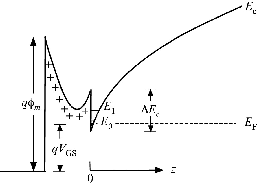
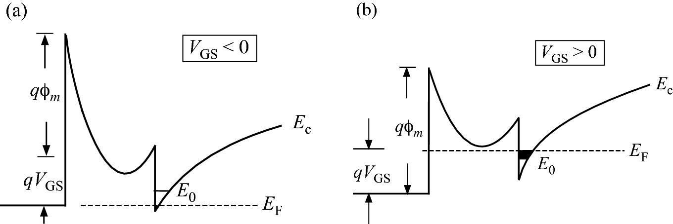
The operation of the HEMT can be best understood through the analysis of its energy band diagram. Unlike MESFETs, the sheet charge density in a HEMT is controlled by the Fermi level position relative to the QW subbands shown in Fig. 9.21. The Fermi level position in the quasi-triangular QW is determined by the work function of the gate metal, barrier layer thickness, doping concentration, conduction band discontinuity, and gate bias. In a properly designed HEMT, through the modulation of the Fermi level, the gate bias voltage VGS directly controls the sheet charge density similar to that of MESFETs. Depending on the device parameters, depletion-mode and enhancement-mode operations of HEMTs are also expected.
../images/325043_1_En_9_Chapter/325043_1_En_9_Fig21_HTML.png
Fig. 9.21

Conduction band diagram of a depletion-mode HEMT under a gate bias of VGS < 0. The work function of the metal contact, m, is also shown

9.4.1 Isolated Heterojunction Under Equilibrium
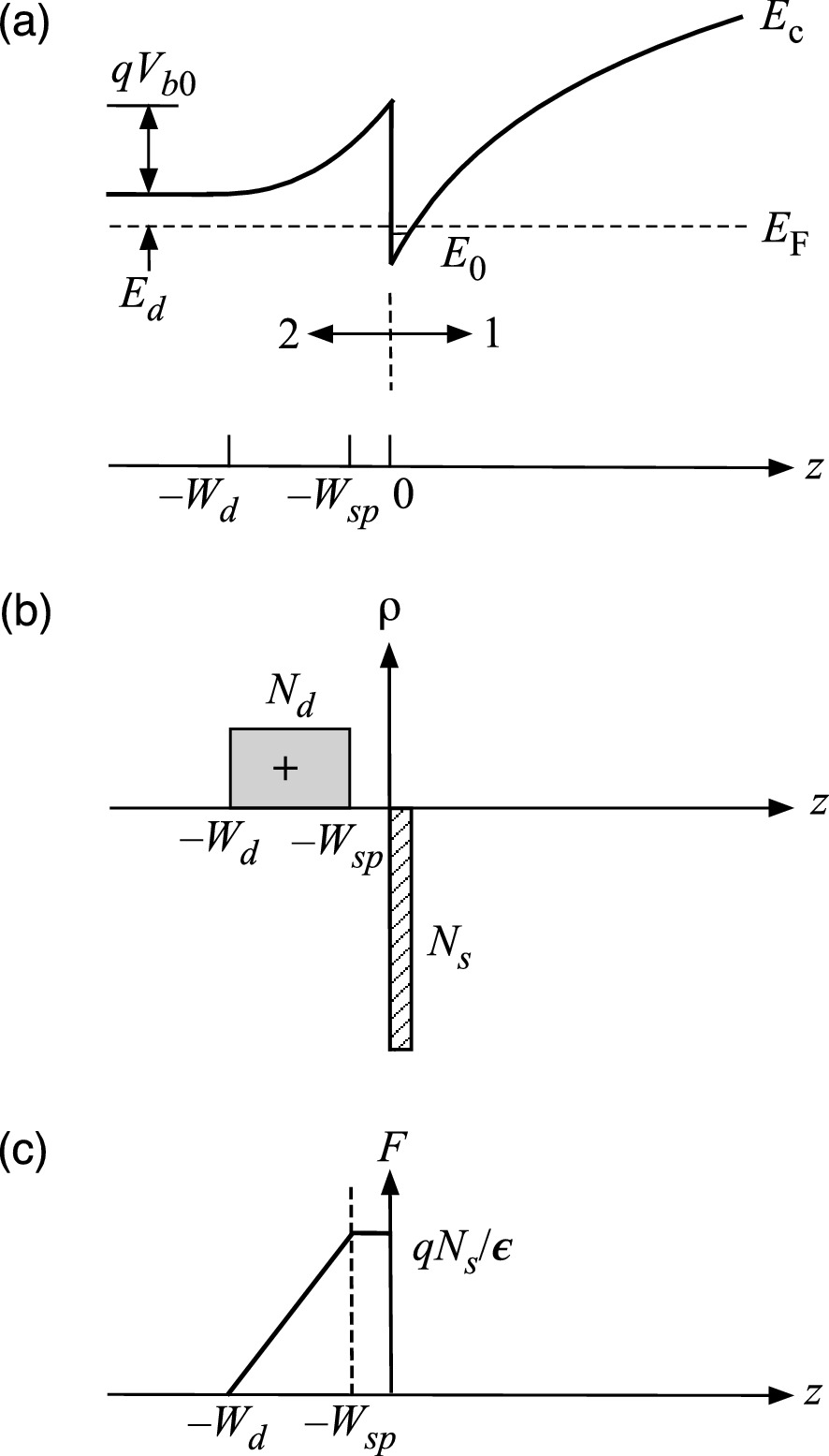
To understand the relationship between the applied gate bias and the Fermi level position or sheet charge density, we first examine the 2DEG heterojunction under equilibrium conditions. In the band diagram shown in Fig. 9.22a, the undoped conduction channel layer and the n-type-doped barrier layer are assigned as regions 1 and 2, respectively. The origin of this 1D diagram is set at the hetero-interface with a depletion width of Wd into the infinite long barrier layer. We also assumed an undoped spacer layer of Wsp on the barrier layer side of the heterojunction, a dopant ionization energy of Ed and a potential barrier height of qVb0 formed by the depletion layer at the hetero-interface.
../images/325043_1_En_9_Chapter/325043_1_En_9_Fig22_HTML.png
Fig. 9.22

a Energy band diagram in conduction band, b charge distribution, and c electric field distribution at the heterojunction of a HEMT

Under equilibrium, according to Gauss’ law, at the hetero-interface, it follows that
$$ D_{1} = D_{2} $$
(9.37)
$$ \epsilon_{1} F_{1} = \epsilon_{2} F_{2} = qN_{S} $$
(9.38)
$$ N_{S} = \epsilon_{2} F_{2} /q $$
(9.39)
where D, F, and $$ \epsilon $$ are the displacement flux density, electric field intensity, and permittivity, respectively. In this section, all discussions concern material 2 only; we will use $$ \epsilon $$ instead of $$ \epsilon_{2} $$ for simplicity.
Assuming donors in the barrier layer are fully ionized between −Wd ≤ z ≤ –Wsp and remain neutral beyond −Wd, Poisson’s equation can be written as
$$ \frac{{{\text{d}}^{2} V}}{{{\text{d}}z^{2} }} = - \frac{{{\text{d}}F}}{{{\text{d}}z}} = - \frac{qN\left( z \right)}{\epsilon } $$
(9.40)
And, as shown in Fig. 9.22b, the charge distribution is
$$ N\left( z \right) = \left\{ {\begin{array}{*{20}l} {0, \quad - W_{sp} &lt; z &lt; 0} \hfill \\ {N_{d} ,  \quad - W_{d} &lt; z &lt; - W_{sp} } \hfill \\ \end{array} } \right. $$
(9.41)
Thus, in the depletion region of the doped barrier
$$ F = \frac{q}{\epsilon }\int N\left( z \right){\text{d}}z = \frac{{qN_{d} }}{\epsilon }z + C $$
(9.42)
Using the boundary condition of F = 0 at z = –Wd, we found (Fig. 9.22c)
$$ F = \frac{{qN_{d} }}{\epsilon }\left( {z + W_{d} } \right)\quad {\text{for}}\quad - W_{d} &lt; z &lt; - W_{{{\text{s}}p}} $$
(9.43)
In the spacer layer, F is a constant of
$$ F = \frac{{qN_{S} }}{\epsilon }\;\quad   {\text{for}}   - W_{sp} &lt; z &lt; 0 $$
(9.44)

The electric field intensity distribution across the depletion region of the heterojunction is shown in Fig. 9.22c.

The electric field intensity in the barrier has a slope of $$ qN_{d} /\epsilon $$. The potential drop across the doped barrier layer (layer thickness ≫ Wd) can then be calculated as
$$ \begin{aligned}   V_{{b{\text{0}}}}  &amp;  =  - \int {F{\text{d}}z}  =  - \frac{{qN_{{\text{d}}} }}{\epsilon }\mathop \int \limits_{{ - W_{{sp}} }}^{{ - W_{d} }} \left( {z + W_{d} } \right){\text{d}}z =  \\     &amp; \quad  - \frac{{qN_{d} }}{\epsilon }\left( {\frac{{z^{2} }}{2} + W_{{\text{d}}} z} \right)_{{ - W_{{sp}} }}^{{ - W_{d} }}  = \frac{{qN_{d} }}{{2\epsilon }}\left( {W_{d}  - W_{{sp}} } \right)^{2}  \\  \end{aligned}   $$
(9.45)
By the same token, the potential drop across the spacer layer becomes
$$ V_{sp} = - \mathop \int \limits_{0}^{{ - W_{sp} }} \left( {\frac{{qN_{S} }}{\epsilon }} \right){\text{d}}z = \frac{{qN_{S} }}{\epsilon }W_{sp} $$
(9.46)
The total potential drop across the barrier is the sum of Vb0 and Vsp.
$$ V = V_{b0} + V_{sp} = \frac{{qN_{d} }}{2\epsilon }\left( {W_{d}^{2} + W_{sp}^{2} } \right) $$
(9.47)

9.4.2 Charge Control by Gate Bias in HEMT
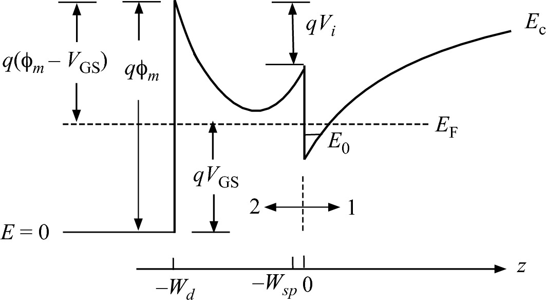
In HEMT structures, the doped barrier layer has a finite thickness and a metal Schottky gate is applied on the surface. The Schottky barrier also creates a surface depletion layer. It substantially alters the conduction band shape of the barrier layer and plays an important role in determining the Fermi level position. To simplify the discussion, assume the doped barrier layer is completely depleted. Relative to the surface, as shown in Fig. 9.23, the potential drop across the barrier is defined as Vi.
../images/325043_1_En_9_Chapter/325043_1_En_9_Fig23_HTML.png
Fig. 9.23

Energy band model of a HEMT under a gate bias VGS < 0. In this model, it is assumed that, under all bias conditions, the barrier layer beneath the gate is completely depleted

$$ V_{i} = \phi_{m} - V_{\text{GS}} - \frac{1}{q}\left( {\Delta E_{\text{c}} - E_{\text{F}} } \right) $$
(9.48)
This potential difference Vi can also be derived from Poisson’s equation.
$$ \frac{{{\text{d}}^{2} V}}{{{\text{d}}z^{2} }} = - \frac{{{\text{d}}F}}{{{\text{d}}z}} = - \frac{qN\left( z \right)}{\epsilon } $$
(9.49)
and
$$ N\left( z \right) = \left\{ {\begin{array}{*{20}c} {N_{d} , \quad - W_{d} \le z \le - W_{sp} } \\ {0, \quad - W_{sp} \le z \le 0} \\ \end{array} } \right. $$
(9.50)
Thus, the electric field intensities in the depleted doped barrier and spacer layers are
$$ F = \frac{q}{\epsilon }\int {N(z)} {\text{d}}z = \left\{ {\begin{array}{*{20}l} \displaystyle{{\frac{{qN_{d} }}{\epsilon} }z + C_{1} ,\quad - W_{d} \le z \le - W_{sp} } \hfill \\ \displaystyle{\frac{{qN_{S} }}{\epsilon }, \quad \quad \quad \quad - W_{sp} \le z \le 0} \hfill \\ \end{array} } \right. $$
(9.51)

Assuming $$ F^{\prime} = qN_{S} /\epsilon = F {\text{at }}z = - W_{sp} ,\;{\text{then}}\;C_{1} = F^{\prime} + qN_{d} W_{sp} /\epsilon $$.

The potential drop across the depleted barrier layer can then be calculated as
$$ \begin{aligned} V &amp; = - \int {F{\text{d}}z} = - \frac{{qN_{d} }}{\epsilon }\mathop \int \limits_{{ - W_{sp} }}^{{ - W_{d} }} zdz - \frac{{qN_{d} W_{sp} }}{\epsilon }\mathop \int \limits_{{ - W_{sp} }}^{{ - W_{d} }} {\text{d}}z - F^{{\prime }} \mathop \int \limits_{{ - W_{sp} }}^{{ - W_{d} }} {\text{d}}z \\ &amp; \quad = - \frac{{qN_{d} }}{\epsilon }\left( {\frac{{z^{2} }}{2}} \right)_{{ - W_{sp} }}^{{ - W_{d} }} - \frac{{qN_{d} W_{sp} }}{\epsilon }\left. z \right|_{{ - W_{sp} }}^{{ - W_{d} }} - F^{{\prime }} \left. z \right|_{{ - W_{sp} }}^{{ - W_{d} }} \\ &amp; \quad = - \frac{{qN_{d} }}{2\epsilon }\left( {W_{d}^{2} - W_{sp}^{2} - 2W_{d} W_{sp} + 2W_{sp}^{2} } \right) + F^{{\prime }} \left( {W_{d} - W_{sp} } \right) \\ \end{aligned} $$
(9.52)
$$ V = - \frac{{qN_{d} }}{2\epsilon }\left( {W_{d} - W_{sp} } \right)^{2} + F^{{\prime }} \left( {W_{d} - W_{sp} } \right) $$
(9.53)
The potential drop across the spacer layer is simply F′Wsp. Letting V(0) = 0, the potential drop Vi can be expressed as
$$  \begin{aligned}   V_{i}  &amp;  =  - V - F^{{\prime }} W_{{sp}}  = \frac{{qN_{d} }}{{2\epsilon }}\left( {W_{d}  - W_{{sp}} } \right)^{2}  - F^{{\prime }} \left( {W_{d}  - W_{{sp}} } \right) \\     &amp; \quad  - F^{{\prime }} W_{{sp}}  = V_{P}  - \frac{{qN_{S} }}{\epsilon }W_{d}  \\  \end{aligned}   $$
(9.54)
Here we defined a pinch-off voltage of $$ V_{P} = \left( {qN_{d} /2\epsilon } \right)\left( {W_{d} - W_{sp} } \right)^{2} $$ just like a MESFET. Since $$ V_{i} = \phi_{m} - V_{\text{GS}} - \left( {\Delta E_{c} - E_{F} } \right) /q $$, we can write the sheet charge density in (9.54) as a function of voltage across the heterostructure.
$$ N_{S} = \frac{\epsilon }{{qW_{d} }}\left[ {V_{\text{GS}} - \left( {\phi_{m} - V_{P} - \frac{{\Delta E_{\text{c}} - E_{\text{F}} }}{q}} \right)} \right] $$
(9.55)
The terms in the parenthesis are all fixed for a particular device structure and are defined as a threshold voltage or off-voltage VT. At an applied gate bias VGS equal to VT, where EF ≤ E0, the 2DEG vanishes.
$$ V_{T} \equiv \phi_{m} - V_{P} - \frac{1}{q}\left( {\Delta E_{\text{c}} - E_{\text{F}} } \right) $$
(9.56)
The Fermi level energy EF is usually small compared with other terms and can be neglected. Finally, the distribution of the 2DEG in the triangular QW has a peak at a distance of ΔW from the heterojunction interface. The effective depletion layer thickness should be corrected as (WdW). For the values of NS between 5×1011 cm−2 and 1.5×1012 cm−2 in AlGaAs/GaAs HEMTs, ΔW is about 80 Å. The final expression of the sheet carrier density becomes
$$ N_{S} \cong \frac{\epsilon }{{q\left( {W_{d} +\Delta W} \right)}}\left( {V_{\text{GS}} - V_{T} } \right) $$
(9.57)
This equation indicates that the 2DEG density is linearly proportional to the gate bias, VGS. This linear relationship is limited by two extremes, NS = 0 and $$ N_{S} = N_{d} \left( {W_{d} - W_{sp} } \right) $$, as illustrated in Fig. 9.24.
../images/325043_1_En_9_Chapter/325043_1_En_9_Fig24_HTML.png
Fig. 9.24

Energy band diagram of a depletion-mode HEMT under different gate biases. a VGS < VT such that the channel is turned off. b Under a high forward gate bias, the 2DEG is saturated

In a HEMT structure with a 2DEG created at zero gate bias, the Fermi level is positioned above the ground state, E0. By applying a reverse gate bias, as shown in Fig. 9.24a, the rise of the total Schottky barrier potential energy at the surface leads to a lowering of EF, which reduces the sheet charge density. When the gate bias is equivalent to the threshold voltage, VT, the conduction channel is turned off. On the other hand, as shown in Fig. 9.24b, under forward gate bias condition, the rising Fermi level allows more electrons to be transferred into the triangular QW, contributing to the current conduction. This process will continue until all donors in the barrier are ionized. The 2DEG sheet carrier density becomes saturated with further increasing of VGS.
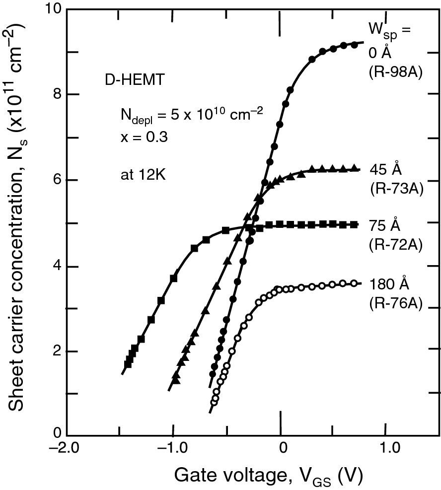
Figure 9.25 shows the experimental results of NS as a function of gate bias in several Al0.3Ga0.7As/GaAs HEMT samples with different spacer layer thicknesses. All samples have a doping concentration of Nd = 4.6×1017 cm−3 in the barrier layer, except sample No. 76 (Nd = 9×1017 cm−3). It is clear, in all samples, that NS increases linearly with increasing VGS and saturates at a higher gate bias voltage. The flat saturated region indicates the maximum achievable sheet carrier density in that sample. By extrapolating the linear part of the VGSNS curve to zero sheet concentration, the threshold voltage is determined. Obviously, the threshold voltage is dependent on the spacer layer thickness due to the VP term involved, which depends on the spacer layer thickness. As expected, for the same device structure, the thinner the spacer layer, the higher the saturated 2DEG density.
../images/325043_1_En_9_Chapter/325043_1_En_9_Fig25_HTML.png
Fig. 9.25

Measured gate-voltage dependence of the sheet carrier density of 2DEG in the GaAs/AlGaAs system. Wsp represents the spacer layer thickness in each sample. All samples have Nd = 4.6 × 1017 cm−3 except sample No. 76, which has Nd = 9.2 × 1017 cm−3.

Reprinted with permission from [6], copyright AIP Publishing

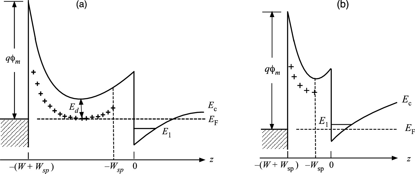
The channel conduction current density of a HEMT is primarily determined by the sheet charge density, which is controlled by the difference between gate bias voltage and threshold voltage. A closer examination of the threshold voltage reveals that it depends on the layer thickness. For a HEMT structure, ϕm and ΔEc are fixed and EF is relatively small. The major term controlling VT is $$ V_{P} = \left( {qN_{d} /2\epsilon } \right)\left( {W_{d} - W_{sp} } \right)^{2} $$, which mainly depends on Wd. Therefore, one can design the operation mode of the device by selecting the proper barrier thickness as shown in Fig. 9.26. For example, a thick barrier (large Wd) leads to a larger VP and a more negative VT. A conduction channel is formed in such a HEMT structure even at zero gate bias (Fig. 9.26a). One has to apply a gate bias equal to VT to completely deplete the 2DEG, thus forming a depletion-mode (normally-on) HEMT. When the barrier layer is reduced to a point such that the Fermi level is well below the ground state (E0) of the triangular QW at zero bias, VT becomes positive. A positive gate bias is required to induce the 2DEG for current conduction, and the HEMT is an enhancement-mode (normally-off) FET (Fig. 9.26b).
../images/325043_1_En_9_Chapter/325043_1_En_9_Fig26_HTML.png
Fig. 9.26

Schematic band diagram at VGS = 0 for a normally-on and b normally-off HEMTs

9.4.3 Current and Voltage Characteristics of HEMT

The drain–source conduction current can be expressed similarly as in a MESFET.
$$ I_{\text{DS}} = qZN_{S} \upsilon_{d} \left( F \right) $$
(9.58)
where Z is the gate width, NS is the 2DEG density, and υd(F) is the electron drift velocity. Since there is a voltage drop, Vx, between source and drain, it should be included in the NS expression of (9.57) as
$$ N_{S} = \frac{\epsilon }{{q\left( {W_{d} +\Delta W} \right)}}\left( {V_{\text{GS}} - V_{T} - V_{x} } \right) $$
(9.59)
Depending on the field strength, the drift velocity along the conduction channel can be modeled with a linear region and a saturation region with the critical field intensity, FC, as the deflection point in the υd versus F plot.
$$ \upsilon_{d} \left( F \right) = \left\{ {\begin{array}{*{20}c} {\mu F\quad {\text{for }}\quad F &lt; F_{C} } \\ {\upsilon_{\text{sat}} \quad {\text{for}}\quad F &gt; F_{C} } \\ \end{array} } \right. $$
(9.60)
In the linear region (F < FC), let $$ F = \displaystyle{\frac{{{\text{d}}V_{x} }}{{{\text{d}}x}}} $$:
$$ I_{\text{DS}} = qZN_{S} \mu F = \frac{\mu \epsilon Z}{{\left( {W_{d} +\Delta W} \right)}}\left( {V_{\text{GS}} - V_{T} - V_{x} } \right)\frac{{{\text{d}}V_{x} }}{{{\text{d}}x}} $$
(9.61)
Since the conduction current in the channel remains constant under a fixed drain bias, the total current can be calculated through integration along the channel length, L.
$$ I_{\text{DS}} \mathop \int \limits_{0}^{L} {\text{d}}x = \mathop \int \limits_{0}^{V_{\text{DS}}} \frac{\mu \epsilon Z}{{\left( {W_{\text{d}} +\Delta W} \right)}}\left( {V_{\text{GS}} - V_{T} - V_{x} } \right){\text{d}}V_{x} $$
(9.62)
Thus, the drain current as a function of drain voltage under fixed VGS is expressed as
$$ I_{\text{DS}} = \frac{\mu \epsilon Z}{{L\left( {W_{d} +\Delta W} \right)}}\left[ {\left( {V_{\text{GS}} - V_{T} } \right)V_{\text{DS}} - \frac{{V_{\text{DS}}^{2} }}{2}} \right] $$
(9.63)

At very low drain bias, the $$ V_{\text{DS}}^{2} $$/2 term is very small and can be neglected. The drain current is linearly proportional to the drain bias. At a sufficiently high drain bias, the $$ V_{\text{DS}}^{2} $$/2 term becomes significant and leads to a sublinear IDS-VGS characteristic. Further increasing the drain bias, the drain current becomes saturated.

The effectiveness of current control by the gate bias voltage is determined by the transconductance, gm. At a fixed VDS, gm is calculated as the variation of drain current per gate bias change.
$$ {\text{g}}_{m} = \left. {\frac{{{\text{d}}I_{\text{DS}} }}{{{\text{d}}V_{\text{GS}} }}} \right|_{{V_{\text{DS}} }} = \frac{{\epsilon ZV_{\text{DS}} }}{{\left( {W_{d} +\Delta W} \right)}}\frac{\mu }{L} \propto \frac{\mu }{L} $$
(9.64)

It is clear that large low-field electron mobility and a short channel length are required for a HEMT to achieve a high gm at a fixed VDS. Within the linear region, gm increases with increasing VDS.

In the saturation region (F ≥ FC), the drift velocity does not increase with the electric field but has a constant value called the saturation velocity, υsat. Therefore, the current becomes a constant, IDS(sat) = qZNsυsat and
$$ \frac{{{\text{d}}I_{\text{DS}} ({\text{sat}})}}{{{\text{d}}V_{\text{DS}} }} = \frac{\mu \epsilon Z}{{L\left( {W_{d} + W} \right)}}\left[ {\left( {V_{\text{GS}} - V_{T} } \right) - V_{\text{DS}} } \right] = 0 $$
(9.65)
From this equation, the threshold saturation voltage is calculated as VDS(sat) = VGSVT. Using this relation in IDS, the IV characteristic in the saturation region is expressed as
$$ I_{\text{DS}} ({\text{sat}}) = \frac{\mu \epsilon Z}{{L\left( {W_{d} +\Delta W} \right)}}\frac{{\left( {V_{\text{GS}} - V_{T} } \right)^{2} }}{2} = \frac{{\mu C_{b} Z}}{L}\frac{{\left( {V_{\text{GS}} - V_{T} } \right)^{2} }}{2} $$
(9.66)
where $$ C_{b} = \epsilon /\left( {W_{d} +\Delta W} \right) $$ is the capacitance per unit area in the barrier. The transconductance in the saturation region can also be derived as
$$ {\text{g}}_{m} = \left. {\frac{{{\text{d}}I_{\text{DS}} \left( {\text{sat}} \right)}}{{{\text{d}}V_{\text{GS}} }}} \right|_{{V_{\text{DS}} }} = \frac{{\mu C_{b} Z}}{L}\left( {V_{\text{GS}} - V_{T} } \right) \propto \frac{\mu }{L} $$
(9.67)

Again, large low-field electron mobility and a short channel length are required to achieve a high gm in the saturation region.

9.4.4 Microwave Noise Performance

The essential elements of the high-speed performance of HEMTs are very similar to those of conventional MESFETs. Therefore, a common microwave equivalent circuit model can be used for both devices. Consider the case where the FET is operating at a frequency below its cutoff frequency, fT, at room temperature. The microwave noise performance of the HEMT can be derived from the equivalent circuit by the same classical noise model of the MESFET. The minimum noise figure Fmin for the HEMT is described as
$$ F_{{\min} } = 1 + K_{f} \left( {f /f_{\text{T}} } \right)\sqrt {{\text{g}}_{m} \left( {R_{\text{G}} + R_{\text{S}} } \right)} $$
(9.68)
where gm, RG, and RS are the transconductance, gate resistance, and source resistance, respectively. Kf is a fitting factor and represents the quality of the channel material. Since all external device parameters for both HEMT and MESFET can be made roughly equal, the noise performance difference between the two devices originates in the Kf difference. It was suggested that the size of Kf is related to excess noise in the drain current, which originates as diffusion noise in the channel. For GaAs MESFETs, Kf ≈ 2. In HEMTs, the electrons are narrowly confined to a quantized state along the interface rather than in a 3D configuration. Monte Carlo simulations indicated much lower diffusion coefficients as a function of electric field than those of MESFETs. Experimental Kf for HEMTs have values between 1 and 2. Therefore, HEMTs have a better microwave noise performance than MESFETs. In addition, since fT can be much higher for HEMTs, we also expect a lower noise figure in HEMTs.

9.5 Optimal Design of the HEMT

Based on discussions above, to achieve high performance, the optimized HEMT structure should incorporate a large ΔEc (≥0.5 eV) for high sheet carrier density NS and high current carrying capability; furthermore, materials with high electron mobility should be selected for efficient high-speed operation, and small gate length (Lg < 0.1 µm) should be used to increase the cutoff frequency. In addition, to enhance electron transfer from the barrier into the triangular QW, a small spacer layer thickness (Wsp ~ 25 Å) is preferred. However, in practice, it was not straightforward to realize all these requirements in the early development of HEMTs. Specifically, the DX center problem severely limited the use of AlxGa1−xAs with high aluminum content (x ≤ 25%) in the HEMT design. In addition, when increasing the barrier doping level to achieve higher 2DEG density, parallel conduction from free electrons trapped in the barrier and 2DEG could form. To overcome these problems, a pseudomorphic layer and delta-doping designs are incorporated to increase ΔEc and 2DEG density.

9.5.1 DX Center in Si-Doped AlGaAs/GaAs HEMT and Delta Doping
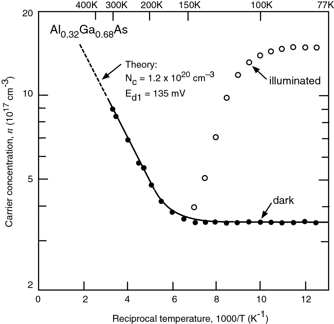
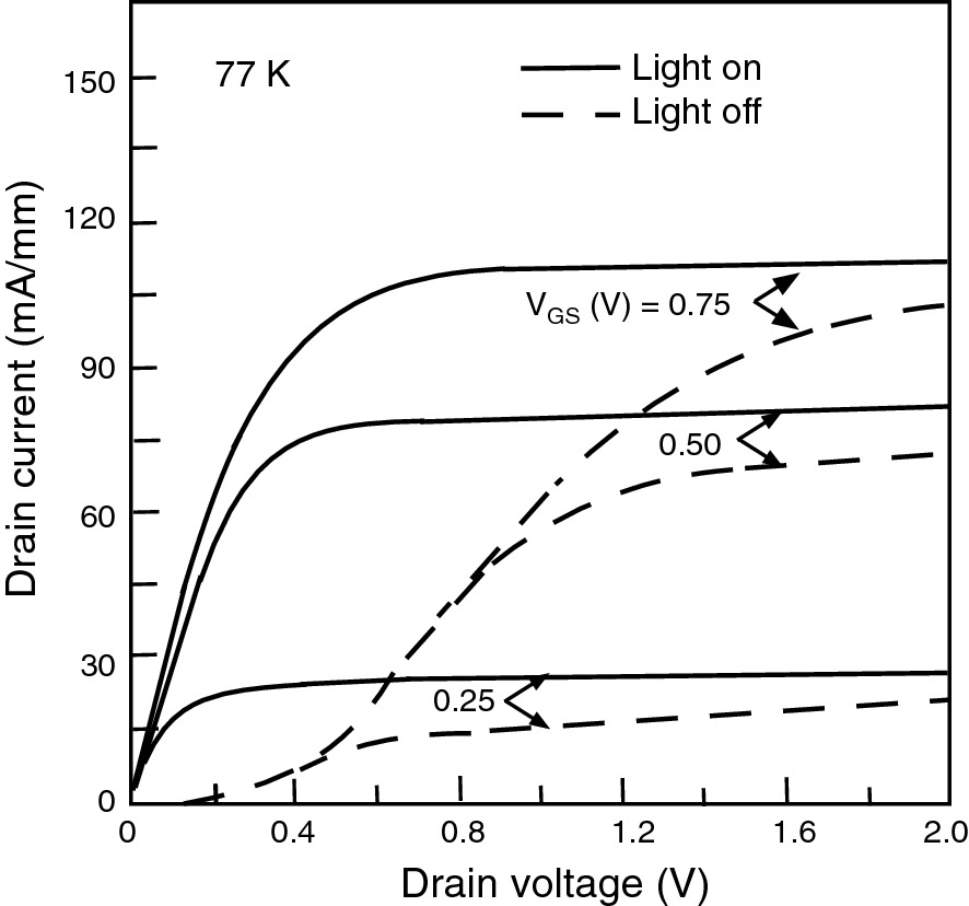
As discussed in Chap. 4, Si-dopants in AlGaAs can take different crystal configurations: interstitial (relaxed state, DX center) or substitutional (excited state). The DX center is a deep trap that requires different energies for capture and emission of electrons. Further, the finite capture barrier makes it difficult to achieve equilibrium at low temperature (<150 K). Depending on the external excitation, the free electron concentration can have different values. For example, in an Al0.32Ga0.68As/GaAs MD structure, the carrier concentration determined by Hall measurement under dark as a function of temperature is shown as solid circles in Fig. 9.27. Upon illumination with a light of energy below the fundamental bandgap of Al0.32Ga0.68As at low temperature, the carrier concentration increases to a high value shown as the open circles. The increase in carrier concentration persists and does not return to its dark value even after the illumination has been turned off. This phenomenon is known as the persistent photoconductivity (PPC) effect. The carrier concentration remains high even hours or days after termination of the photo-excitation. The high PPC carrier concentration can be quenched by heating the sample to a temperature higher than 150 K. In Si-doped AlGaAs/GaAs HEMT structures, DX centers can cause anomalous device behaviors including threshold voltage shifts and ‘collapse’ of IV characteristics (Fig. 9.28). These properties degrade the HEMT performance severely and make the device unreliable.
../images/325043_1_En_9_Chapter/325043_1_En_9_Fig27_HTML.png
Fig. 9.27

Dependence of the Hall electron concentration in n-type Al0.32Ga0.68As:Si on reciprocal temperature. Solid and open circles indicate experimental data measured in the dark and after illumination at low temperatures, respectively.

Reprinted with permission from [7], copyright AIP Publishing
../images/325043_1_En_9_Chapter/325043_1_En_9_Fig28_HTML.png
Fig. 9.28

IV characteristics of a HEMT at 77 K under illumination and in darkness. The degradation of the characteristics upon the elimination of light occurred gradually over a period of 20–30 s.

Reprinted with permission from [8], copyright IEEE
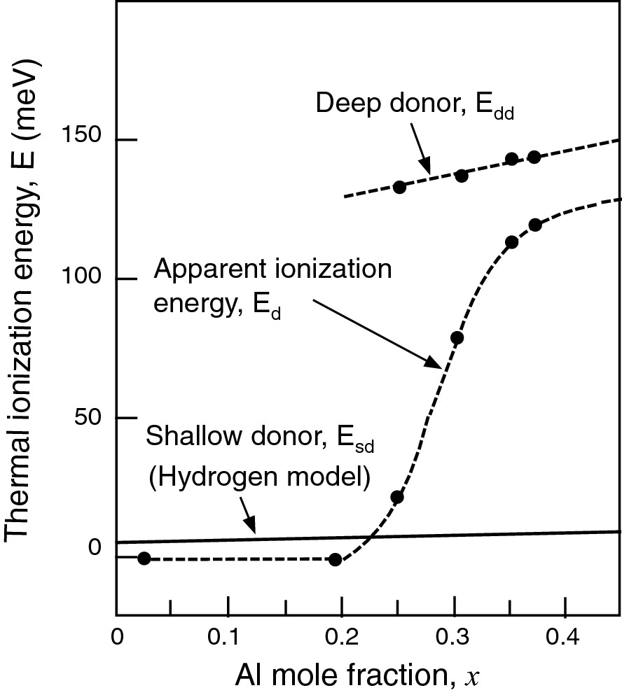
The origin of the DX center problem is closely related to the ionization energy of Si donors in AlxGa1−xAs, which is shown in Fig. 9.29. For Al-composition of x ≤ 20%, the Si donor behaves like a shallow donor (Ed ≤ 5 meV) and no DX center related problem is observed. For x ≥ 30%, the ionization energy of the Si donor rises rapidly to ≥120 meV such that it acts like a deep donor and causes DX center problems.
../images/325043_1_En_9_Chapter/325043_1_En_9_Fig29_HTML.png
Fig. 9.29

Thermal ionization energy of the Si donor as a function of the Al mole fraction in AlxGa1−xAs.

Reprinted with permission from [7], copyright AIP Publishing

For example, in an AlxGa1−xAs/GaAs HEMT with a composition of x = 30%, the donor level, Ed, is 0.12 eV below the conduction band. Since Ed is very deep, under dark, a portion of the donor level inside the barrier is below the Fermi level and stays neutral (unionized). Only a thin-doped barrier layer adjacent to the spacer layer is contributing electrons to the 2DEG channel and the sheet charge density is very low. The neutral layer in the barrier also decouples the 2DEG and the surface. Therefore, NS in 2DEG is independent of bias! When illuminated with a light source having energy less than the bandgap, electrons are excited out of DX centers. All the donors are ionized and the 2DEG has risen. Due to the finite electron trapping barrier height, there are free electrons remaining in the barrier at low temperatures and these form ‘parallel conduction’ channel in addition to the 2DEG conduction.
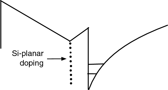
Since the ionization energy of Si dopants increases rapidly with increasing Al-composition in AlGaAs-based HEMT structures, ΔEc cannot be increased much beyond 20%. To achieve a high sheet charge density, increasing the doping level of the AlGaAs barrier layer is the other alternative. But a large and excessive Nd can lead to gate leakage and parallel conduction, which degrade the device performance. One simple solution to this problem is to use a planar (pulse or delta) doping scheme. The doping impurities are all deposited on the same growth plane such that the impurity distribution is confined in a sheet layer. Since the barrier is undoped except for the doping sheet, the band profile shows a straight line-like variation (Fig. 9.30). The planar-doped sheet locates at the minimum of the conduction band profile in the barrier. Since the AlGaAs barrier layer is undoped, it not only solves the gate leakage and parallel conduction problems but also minimizes the DX center-induced complications of the HEMT structure.
../images/325043_1_En_9_Chapter/325043_1_En_9_Fig30_HTML.png
Fig. 9.30

Schematic energy band diagram of Si-planar doping in a MD structure

9.5.2 Pseudomorphic High-Electron-Mobility Transistors (pHEMT)
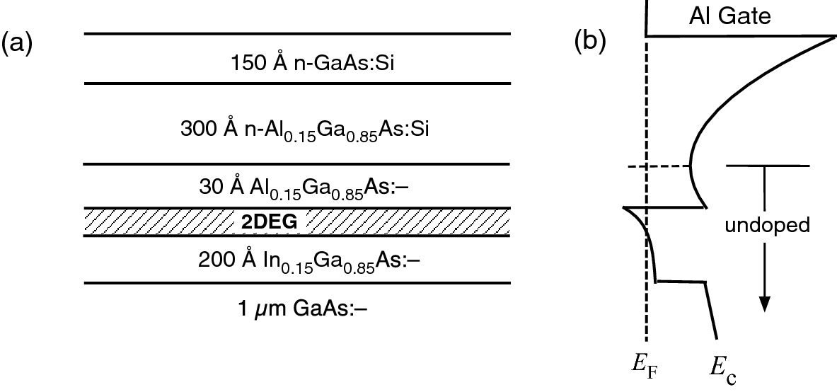
Since NS in 2DEG is in proportion with the conduction band discontinuity (ΔEc) at the heterojunction, a large ΔEc is essential for a high sheet electron density. In AlGaAs/GaAs HEMTs, we cannot increase ΔEc by increasing the Al-composition much beyond 20% due to the DX center problem. This limitation can be relaxed by using a thin layer of strained InGaAs to replace GaAs at the heterojunction as the 2DEG conduction channel layer (Fig. 9.31). The ΔEc increases almost linearly with increasing In composition. The amount of indium composition in the InGaAs layer grown on GaAs is limited only by the critical layer thickness such that no dislocations are generated in the channel layer. This type of strained layer HEMT structure is called the pseudomorphic HEMT or pHEMT. The other advantage of using InGaAs as the conduction channel is the associated electron mobility which is higher than that of GaAs. These advantages make AlGaAs/InGaAs pHEMT the most commonly used device in high-speed applications. To further enhance the high-speed operation properties beyond AlGaAs/InGaAs pHEMT, the AlInAs/InGaAs/InP material system is preferred due to the high electron mobility of the In-rich InGaAs channel material.
../images/325043_1_En_9_Chapter/325043_1_En_9_Fig31_HTML.png
Fig. 9.31

a Schematic of InGaAs/AlGaAs pseudomorphic HEMT. b Conduction band diagram of the pHEMT

9.6 GaN-Based HEMT Structures

The rapid expansion of wireless communications worldwide has increased the demand for high-power electronic devices in both terrestrial base stations and satellite communication systems. Current GaAs-based FETs have been dominating the market for many years, but the increase in demand calls for devices with higher power operation capacity at microwave frequencies. Among all semiconductors, the GaN-based material system has shown great potential in high-power and high-frequency device applications. Some of the key device properties of GaN- and GaAs-based HEMTs are compared in Table 9.2. Because of their high breakdown voltages, GaN-based HEMTs are ideal for high voltage operation, reducing the need for voltage conversion. This makes device integration much simpler. Another attractive fact is that GaN has a high saturation electron velocity suitable for high-frequency operation. Its great thermal conduction properties and large maximum 2DEG density (≥1013/cm2) translate into much higher power densities, making it ideal for high-power operation. In addition, GaN devices can also operate at higher temperatures than their GaAs counterparts because of the higher energy bandgap (~3.4 eV). All these properties make the GaN-based HEMT an ideal candidate for high-power operation at microwave frequencies. However, there are major differences between GaN-HEMT device structures and those of other III–V HEMTs. First, no doping in the AlGaN barrier layer is needed to generate the 2DEG in the GaN channel layer and, second, the generation of the 2DEG is heterostructure dependent.
Table 9.2

Material parameters of GaN and GaAs

Material parameters

GaN

GaAs

Bandgap energy (eV)

3.438

1.424

Maximum sheet electron density (cm−2)

1–5 × 10¹³

2–3 × 10¹²

Breakdown field strength (105 V/cm)

50

4

2DEG mobility (cm2/V s)

2000

8500

Saturation electron velocity (107 cm/s)

2.5

1.0

Thermal conductivity (W/cm K)

≥2.1

0.44

9.6.1 Polarization-Induced Sheet Charges at Heterojunctions

GaN-based HEMT layer structures are currently grown using either MBE or MOCVD. MBE layers are usually grown directly on (0001) sapphire or c-Al2O3 under Ga-rich surface conditions to achieve a high layer quality. This particular MBE growth condition yields N-terminated B-face or N-face layers, i.e., the GaN growth direction is along [000$$ \bar{1} $$] capped with a top nitrogen plane (Fig. 9.32). In the MOCVD approach, a low-temperature-grown AlGaN nucleation layer on (0001) sapphire is needed before the growth of GaN. The nitrogen-rich growth condition for the nucleation layer yields a Ga-terminated A-face or Ga-face layer and a growth direction along [0001] capped with a top gallium plane. This growth direction is opposite to the MBE-grown nitrides and causes a sign change in spontaneous polarization.
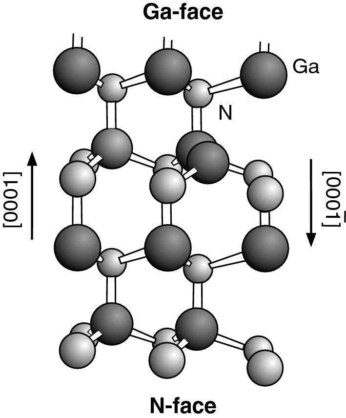
../images/325043_1_En_9_Chapter/325043_1_En_9_Fig32_HTML.png
Fig. 9.32

Schematic diagram of the crystal structure of wurtzite Ga-face GaN.

Reprinted with permission from [9], copyright AIP Publishing

Using an III–N heterostructure grown by MOCVD as an example, we can examine contributions of spontaneous polarization and piezoelectric polarization in the structure to the generation of 2DEG at hetero-interfaces. An AlGaN/GaN heterostructure is grown on c-Al2O3 with a thin AlGaN nucleation layer deposited first. The GaN channel layer is grown next and finished by depositing a thin AlxGa1−xN barrier layer. The whole heterostructure is intentionally undoped. Since MOCVD-grown AlGaN has a Ga-face surface, PSP is pointing in the [000$$ \bar{1} $$] direction toward the substrate and has a negative value for all compositions. Here we assumed the polarization along the c-axis or [0001] toward surface is positive. The AlGaN/GaN heterostructures grown by MOCVD and MBE and their polarization components are shown in Fig. 9.33. The magnitude and sign of PPE depend on the strain condition. The thick GaN channel layer is relaxed and has a zero piezoelectric polarization component. Since AlGaN has a smaller lattice constant than GaN, the thin AlGaN barrier layer is under tensile strain and PPE has a negative value. Therefore, the net polarization P is negative at the AlGaN/GaN interface. If the polarity flips over from Ga-face to N-face in structures grown by MBE, both PSP and PPE change their signs.
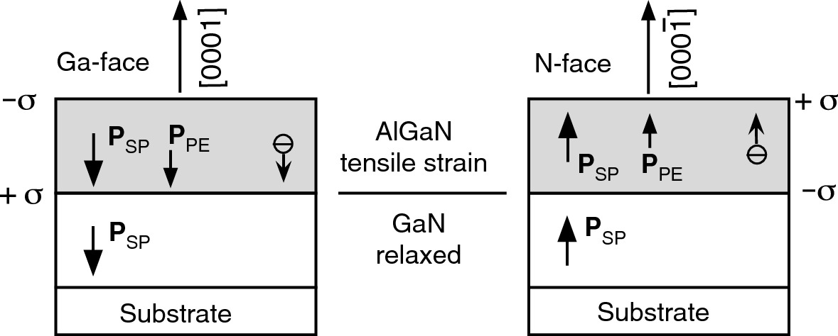
../images/325043_1_En_9_Chapter/325043_1_En_9_Fig33_HTML.png
Fig. 9.33

Polarization-induced sheet charge density (σ) and directions of the spontaneous (PSP) and piezoelectric (PPE) polarization in Ga- and N-face tensile strained AlGaN/GaN heterostructures grown by MOCVD (left) and MBE (right).

Reprinted with permission from [9], copyright AIP Publishing

Associated with a nonzero polarization P= P$$ \hat{z} $$ in a dielectric slab is an induced internal electric field F, which is produced by the fictitious surface charge density  $$\sigma = \hat{\varvec{n}} \cdot  \varvec{P} $$, where $$ \hat{\varvec{n}}   $$ is the surface unit vector. By Gauss’ law, the electric field between the plates produced by these charges is $$ \varvec{F} = - \varvec{P} /\epsilon $$. In analog, the net polarization change within the AlGaN/GaN bilayer heterostructure under discussion induces sheet charge densities at the hetero-interface and on the surface of AlGaN defined as
$$ \sigma = P\left( {\text{bottom}} \right) - P\left( {\text{top}} \right) $$
$$ = \left[ {P_{\text{SP}} \left( {\text{bottom}} \right) + P_{\text{PE}} \left( {\text{bottom}} \right)} \right] - \left[ {P_{\text{SP}} \left( {\text{top}} \right) + P_{\text{PE}} \left( {\text{top}} \right)} \right] $$
(9.69)

In this heterostructure, the top surface of AlGaN and the underneath AlGaN/GaN hetero-interface carry −σ and +σ, respectively. During the cooling process, after the epitaxial growth, the polarization-induced positive sheet charge, +σ, will attract free electrons to compensate it and form a 2DEG at the hetero-interface. If the heterostructure is grown by MBE, resulting in an N-face material, the piezoelectric polarization, along with the spontaneous polarization, changes its sign. A negative sheet charge, −σ, will form at the AlGaN/GaN hetero-interface and attract holes. To utilize the fictitious positive sheet charge to induce 2DEG on the AlGaN surface, a GaN layer is needed on top of the AlGaN/GaN heterostructure.

9.6.2 Sheet Carrier Concentration of 2DEG
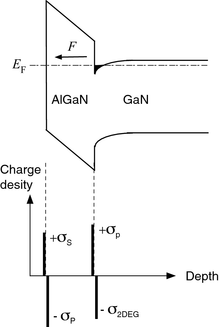
When Schottky gate contact is made to the surface of the AlGaN barrier layer, the heterostructure with a Ga-face surface forms a HEMT structure. The equilibrium energy band diagram and sheet charge density (σi) of the HEMT structure are shown in Fig. 9.34. At equilibrium, due to the band bending across the barrier layer, the Schottky barrier induces an electric field in AlGaN and a net charge density is required to terminate the electric field. The size of the electric field is fixed by the potential drop in the AlGaN determined by the Fermi level position at the surface and at the hetero-interface. Thus, the 2DEG density at the hetero-interface departs somewhat from the polarization-induced electron density. The modified 2DEG carrier density is expressed as
../images/325043_1_En_9_Chapter/325043_1_En_9_Fig34_HTML.png
Fig. 9.34

Band diagram of an AlGaN/GaN HEMT structure grown on Ga-face GaN. The sheet charge density distributions in the structure are also shown. σp, σ2DEG, and σs are induced piezoelectrical, 2DEG, and surface charge densities, respectively

$$ n_{S} \left( x \right) = \frac{{\sigma_{{ 2 {\text{DEG}}}} }}{q} = \frac{{\sigma_{p} \left( x \right)}}{q} - \frac{\epsilon \left( x \right)}{{q^{2} d}}\left[ {q\phi_{m} \left( x \right) -\Delta E_{\text{c}} \left( x \right) + E_{\text{F}} \left( x \right)} \right] $$
(9.70)
where σp is a piezoelectrically induced charge density at the AlGaN/GaN interface, $$ \epsilon $$ is the dielectric constant of AlGaN barrier, d is the barrier thickness, m is the Schottky barrier height of a gate contact, ΔEc is the conduction band offset at the AlGaN/GaN interface, and EF is the Fermi level with respect to the GaN conduction band-edge energy. To determine the net sheet charge density from the polarization-induced 2DEG, we use the following approximations.
For AlxGa1−xN, ΔEc(x) ≈ 2.12x and Eg(x) = xEg(AlN) + (1–x)Eg(GaN) − 0.7x(1–x). The dielectric constant is expressed as $$ \epsilon $$(x) = 9.5 − x, and m(x) = 1.3x + 0.84 (eV). The Fermi energy has the form of
$$ E_{\text{F}} \left( x \right) = E_{0} \left( x \right) + \frac{{\pi \hbar^{2} }}{{m^{*} \left( x \right)}}n_{S} \left( x \right) $$
(9.71)
where E0(x) is determined from the Airy function and m*(x) = 0.22me. Using the piezoelectric-induced sheet charge density expression of
$$ \sigma_{p} \left( x \right) = \left[ {P_{\text{SP}} \left( {\text{GaN}} \right)} \right] - \left[ {P_{\text{SP}} \left( {\text{AlGaN}} \right) + P_{\text{PE}} \left( {\text{AlGaN}} \right)} \right], $$
and polarizations from (7.​128) to (7.​131)
$$ P_{\text{SP}} \left( {{\text{Al}}_{x} {\text{Ga}}_{1 - x} {\text{N}}/{\text{GaN}}} \right) = - 0.090x - 0.034\left( {1 - x} \right) + 0.021x\left( {1 - x} \right)\;{\text{c/m}}^{2} $$
$$ P_{\text{PE}} \left( {{\text{Al}}_{x} {\text{Ga}}_{1 - x} {\text{N}}/{\text{GaN}}} \right) = - 0.0525x + 0.0282x\left( {1 - x} \right)\;{\text{c/m}}^{2} $$
the 2DEG density can be obtained.
Figure 9.35 displays the calculated 2DEG sheet charge density as a function of Al-composition x for 10, 20, and 30 nm AlGaN barriers using parameters available at the time of report [9]. Nevertheless, the results give a meaningful insight into and design guidelines for the AlGaN/GaN HEMT. They show that the piezoelectric effect leads to the formation of a high-density 2DEG (~1013 cm−2) in AlGaN HEMT structures without intentional doping. In fact, the sheet charge densities in nominally undoped nitride HEMTs can be comparable to those achievable in doped-channel FET structures, but without the degradation in mobility resulting from the presence of ionized impurities in the channel. The 2DEG sheet charge density can go even higher by increasing the Al-composition x in the barrier layer. However, for high crystal quality, the large lattice-mismatch between AlN and GaN prevents it from using x ≥ 40% in the AlxGa1−xN barrier. On the other hand, for x < 15%, the conduction band offset becomes too low to confine the 2DEG. Therefore, an optimal composition of AlxGa1−xN barrier for maximum 2DEG sheet charge density is limited to 0.15 < x < 0.4. The inset compares the maximum sheet charge density of a pseudomorphic grown Ga-face AlGaN/GaN and an N-face GaN/AlGaN heterostructure. The figures show similar trends in the useful composition range.
../images/325043_1_En_9_Chapter/325043_1_En_9_Fig35_HTML.png
Fig. 9.35

Sheet carrier concentration of the 2DEG confined at a Ga-face GaN/AlGaN/GaN or N-face GaN/AlGaN/GaN interface for different thicknesses of the AlxGa1−xN barrier. The inset shows the maximum sheet carrier concentration of a pseudomorphically grown Ga-face AlGaN/GaN and an N-face GaN/AlGaN heterostructure.

Reprinted with permission from [9], copyright AIP Publishing
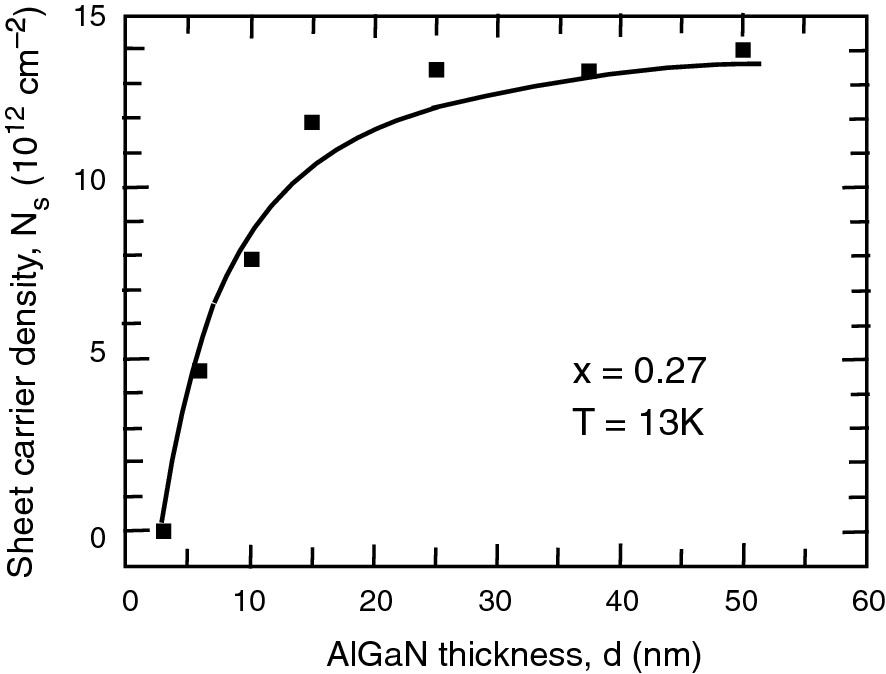
Since the 2DEG in AlGaN HEMT structure is generated by polarization, it requires a minimum strain in the AlGaN barrier, which can be controlled by adjusting the composition and/or the layer thickness. The higher Al composition x in AlGaN causes a larger strain leading to a greater polarization as well as a greater conduction band-edge discontinuity. Therefore, the resultant 2DEG density increases with increasing x for a fixed barrier thickness. On the other hand, for a fixed x, the lattice-mismatch-induced strain increases with the barrier layer thickness, which, in turn, increases the polarization. As shown in Fig. 9.36, for x = 0.27, the induced 2DEG sheet charge density becomes significant only after the barrier thickness is larger than ~5 nm and increases rapidly thereafter. However, the 2DEG density also depends on the efficiency of carrier transfer across the undoped AlGaN barrier, and it prefers a thin AlGaN for easy transfer of sheet charges. Thus, the barrier layer thickness increases beyond ~15 nm, the 2DEG sheet charge density does not increase appreciably and saturates gradually.
../images/325043_1_En_9_Chapter/325043_1_En_9_Fig36_HTML.png
Fig. 9.36

2DEG sheet carrier density in the Al0.27Ga0.73N/GaN structures as a function of AlGaN barrier width.

Reprinted with permission from [10], copyright AIP Publishing
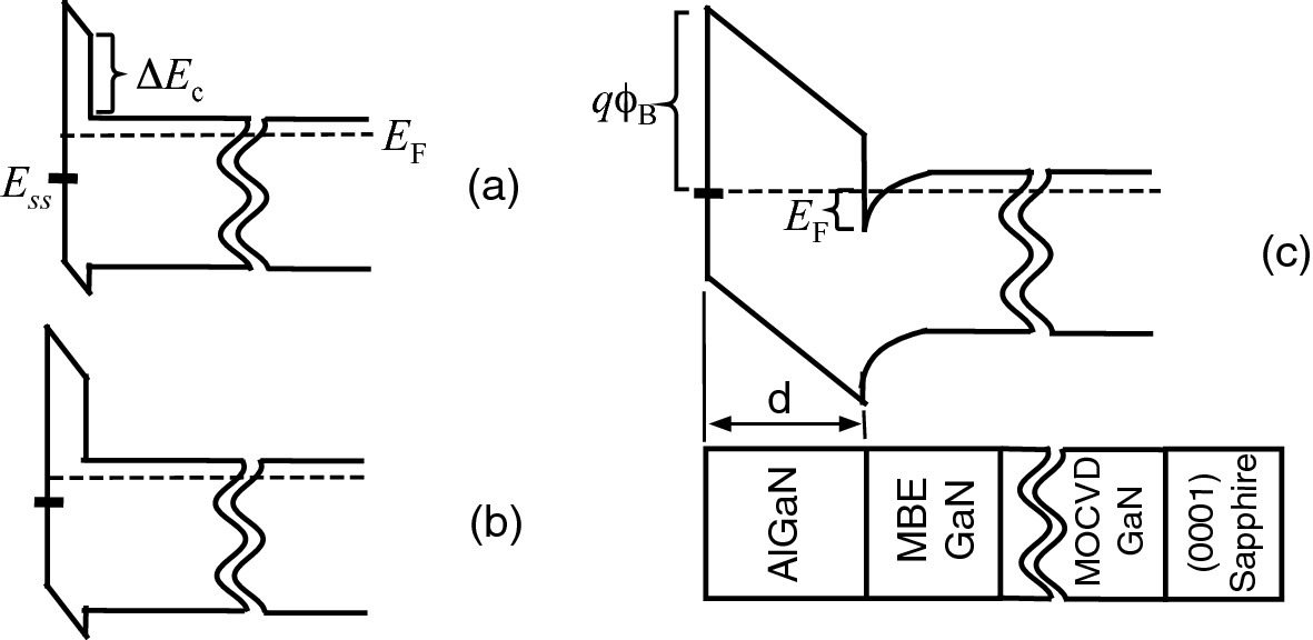
Now, we have to answer the question: Where do those high-density 2DEG carriers come from in such an undoped structure? Experiments have been carried out to rule out the possibility of the residual impurities in the undoped heterostructure as the source. It turns out that the donor-like surface states Ess located ~1.5 eV below the conduction band edge of the AlGaN are the source of the 2DEG, as seen from the band diagrams shown in Fig. 9.37. In an AlGaN HEMT structure with a very thin barrier, the energy band edge maintains a near flat band configuration and EF ≫ Ess. No 2DEG is formed. When increasing the AlGaN barrier thickness, a greater potential drop is developed and the surface Ess increases accordingly. For thin AlGaN barriers, Ess is still below EF and no 2DEG forms (Fig. 9.37b). Only after the AlGaN barrier thickness reaches a threshold such that Ess ≥ EF and electrons associated with the donor-like surface states are ready to transfer to the hetero-interface does the 2DEG form (Fig. 9.37c).
../images/325043_1_En_9_Chapter/325043_1_En_9_Fig37_HTML.png
Fig. 9.37

Schematic diagram showing the development of the band structure in AlGaN/GaN samples with increasing AlGaN barrier width.

Reprinted with permission from [10], copyright AIP Publishing

9.7 Heterojunction Bipolar Transistors (HBTs)

9.7.1 Introduction

The idea of using heterostructure at the emitter–base junction in a bipolar junction transistor (BJT) is not new. It was pointed out and patented by William Shockley at the time of the invention of the bipolar transistor at Bell Labs that a large bandgap emitter can be used to increase the efficiency of the device. US Patent 2,569,347 issued to W. Shockley (filed on June 26, 1948; expired on Sept. 24, 1968) claimed.

Claim 2

A device as set forth in claim 1 in which one of the separated zones is of a semiconductor material having a wider energy gap than that of the material in the other zones

Herb Kroemer proposed the first heterojunction bipolar transistor (HBT) structure in 1957 [11]. Like other heterostructure devices, the HBT technology has been progressing rapidly only after the material growth technologies were matured. Currently, the highest operation frequency of fT > 800 GHz has been demonstrated in InP/InGaAs HBTs [12]. New functions, such as high-speed spontaneous and stimulated light emission, have also been demonstrated in HBTs (light-emitting transistors and transistor lasers) [13].

The HBT inherits all the advantages of the BJT including high cutoff frequency due to the short transient time across the thin base region, uniform turn-on voltage which is determined by the built-in potential of the junction, high power capability resulting from the entire emitter area conducting current, and high transconductance which enables low-power applications. By adding a heterojunction to the BJT, additional advantages emerge. The energy band discontinuity at the emitter–base (EB) heterojunction of a HBT suppresses the diffusion of majority carriers from the base into emitter for higher gain. The EB heterojunction also allows the use of a highly doped base region for low base sheet resistance without lowering gain. This means a very thin base layer can be used for a shorter transient time to achieve a higher cutoff frequency. It is expected that HBTs have higher current gain and cutoff frequency than BJT.

At the onset of HBT development, only one heterojunction was used at the EB junction of a single heterojunction bipolar transistor (SHBT). The emitter region of the GaAs-based SHBT is replaced by a larger bandgap AlGaAs, and the base–collector (BC) junction remains a GaAs homojunction. To enhance the breakdown voltage performance of a HBT, a larger bandgap material, such as AlGaAs, is used in the collector region. In this case, both EB and BC junctions are replaced by AlGaAs/GaAs heterojunctions to form a double-heterojunction bipolar transistor (DHBT). Currently, HBTs using different material systems have been developed including InxGa1−xP/GaAs, InP/InxGa1−xAs, Si/SixGe1−x, and InP/GaAs xSb1−x for various applications. Obviously, heterojunctions with either type-I or type-II energy band discontinuity can be used in HBT designs.

9.7.2 Basic Theory of Heterojunction Bipolar Transistors
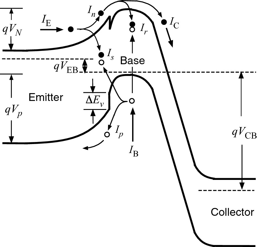
The energy band diagram of a type I N-p+-n SHBT under normal operation is shown in Fig. 9.38. To generalize the discussion, the hetero-interface of the HBT is graded such that the effect of the EB junction energy spike in the conduction band is neglected. The energy bandgap of the emitter and base are EgN and Egp, respectively. A forward bias voltage of VEB and a reverse bias voltage of VCB are applied to EB and BC junctions, respectively. The terminal currents of the SHBT are the emitter current IE, base current IB, and collector current IC. These currents are related to internal current components of the injected electron current into base (In), the injected hole current into emitter (Ip), the saturation current at the EB junction (Is), and the recombination current in the base region (Ir) through the following equations:
../images/325043_1_En_9_Chapter/325043_1_En_9_Fig38_HTML.png
Fig. 9.38

Energy band diagram of an N-p-n HBT, under normal mode operation, showing the various current components and the hole-blocking effect of the valence band discontinuity ΔEv at the EB junction

$$ \left\{ {\begin{array}{*{20}c} {I_{\text{E}} = I_{n} + I_{s} + I_{p} } \\ {I_{\text{B}} = I_{p} + I_{r} + I_{s} } \\ {I_{\text{C}} = I_{n} - I_{r}         } \\ \end{array} } \right. $$
(9.72)
The above discussions can also apply to BJTs by simply setting EgN = Egp. The ratio of the collector current and base current defines the current gain of the junction transistor.
$$ \beta = \frac{{I_{\text{C}} }}{{I_{\text{B}} }} = \frac{{I_{n} - I_{r} }}{{I_{p} + I_{r} + I_{s} }} $$
(9.73)
To maximize β, the components in the numerator and denominator need to be maximized and minimized, respectively. The maximum current gain (βmax) is simply the ratio In/Ip in the limit of negligible recombination losses. Assuming a non-degenerate case, the approximate injection electron and hole current densities at the EB junction are
$$ J_{n} = qn_{\text{B}} \upsilon_{{n{\text{B}}}} = qN_{\text{E}} \upsilon_{{n{\text{B}}}} \text{exp}\left( { - qV_{N} / {kT}} \right) $$
(9.74a)
$$ J_{p} = qp_{\text{E}} \upsilon_{{p{\text{E}}}} = qp_{\text{B}} \upsilon_{{p{\text{E}}}} \exp \left( { - qV_{p} / {kT}} \right) $$
(9.74b)
where NE and pB are the doping level in the emitter and base, respectively; υnB is the electron mean velocity in the base near the EB junction; υpE is the hole mean velocity in the emitter near the EB junction; and qVN and qVp are the potential barrier height for electrons and holes, respectively. At the heterojunction, q(VpVN) = EgNEgp = ΔEg, we obtain the maximum current gain (βmax)
$$ \beta_{{\max} } = \frac{{I_{n} }}{{I_{p} }} = \frac{{N_{\text{E}} }}{{p_{\text{B}} }}\frac{{\upsilon_{{n{\text{B}}}} }}{{\upsilon_{pE} }}\exp \left( {\Delta E_{\text{g}} / {kT}} \right) $$
(9.75)
The mean velocity ratio of (υNB/υpE) is the least subject to manipulation. To achieve large βmax (>100), it is necessary that either NE ≫pB or ΔEg > kT. Energy gap differences that are several kT are readily available. Due to the exponential nature of the (ΔEg/kT) term, it dominates βmax even if NE < pB. Therefore, using heterojunction structures with large ΔEg, very high maximum current gain can be achieved regardless of the emitter-to-base doping ratio. It simply means that the hole injection current Ip is sufficiently suppressed by a large ΔEv and becomes a negligible part of the base current compared to the two recombination currents: IB ≈ Is + Ir. If we approximate IE by In, we obtain
$$ \beta \cong \frac{{I_{n} }}{{I_{r} + I_{s} }} $$
(9.76)
In a HBT with a highly doped base, the recombination current Ir is the dominant current component since the saturation current Is ≪ In for a high-quality interface. At the same time, the very high doping density translates into a rather short minority carrier lifetime in the base region. Therefore, the bulk recombination current Ir, rather than the interface recombination current Is, will dominate the base current. Thus, IB ≈ Ir and equals the total minority carriers (Qn) stored in the base divided by the minority carrier lifetime (τn):
$$ I_{r} \approx \frac{{Q_{n} }}{{\tau_{n} }} = \frac{{qAn_{\text{B}} W_{\text{B}} }}{{2\tau_{n} }} = \left( {\frac{{qAW_{\text{B}} }}{{2\tau_{n} }}} \right)N_{\text{E}} \exp \left( { - qV_{N} / {kT}} \right) $$
(9.77)
where A is the cross-sectional area of the EB junction and WB is the base width of the device. The current gain of a HBT structure with a large ΔEg and high quality interfaces becomes
$$ \beta \equiv \frac{{I_{n} }}{{I_{r} }} = \frac{{N_{\text{E}} \upsilon_{{n{\text{B}}}} \exp \left( { - qV_{N} / {kT}} \right)}}{{\left( {W_{\text{B}} /2\tau_{n} } \right)N_{E} \exp \left( { - qV_{N} / {kT}} \right)}} = \frac{{2\tau_{n} \upsilon_{{n{\text{B}}}} }}{{W_{\text{B}} }} $$
(9.78)

The effect of the base doping on the minority carrier lifetime and the base width in turn directly affects the current gain. Even if for heavy base doping levels the lifetimes may be short, high β’s should be achievable in HBTs with sufficiently thin base region. Furthermore, in a thin base HBT, the electron velocity is likely to approach its saturation velocity of ~107 cm/s, enhancing the current gain. As a result, no serious concerns arise from reduced minority carrier lifetime in HBTs with heavily doped thin (≤ 100 nm) base region.

Now we can examine the current gain property of a BJT. In homojunction bipolar junction transistors, ΔEg = 0. The only way to achieve high current gain is to make NE ≫pB. Since the base doping level is kept low, it requires a thick base layer to minimize the base sheet resistance. A thick base layer will eventually limit the cutoff frequency of the BJT. On the other hand, the doping level in the emitter cannot exceed certain limits. A heavily doped emitter will cause other problems. When the emitter degenerates, the Fermi level can move into the conduction band and cause bandgap shrinkage. This is equivalent to a reduction of conduction band discontinuity at the EB junction or ΔEg < 0. A lowering of βmax is expected. Therefore, the HBT takes advantage of the exponential dependency of ΔEg to achieve high gain with high base doping concentration. Furthermore, the doping profile of the BJT is graded due to diffusion and/or ion implantation processes used in device fabrication. For HBTs, a much sharper doping profile is achieved by controlling doping properties during epitaxy. The abrupt and heavily doped base region is desirable for achieving high current gain and high cutoff frequency in a HBT. Thus, it is critical to use a suitable p-type dopant that possesses a high doping efficiency and a low diffusivity. For GaAs-based HBTs, carbon has proved to be an ideal p-type dopant among other common candidates such as Zn and Be. It can be easily doped to over 1020 cm−3 in many III–V compound semiconductors with negligible out-diffusion. However, carbon atoms are hard to generate from a solid source, such as graphite, due to their extremely low vapor pressure. Currently, the heavily p-type carbon doping is conveniently achieved using gaseous carbon sources such as CCl4 (in MOCVD) and CBr4 (in MBE).
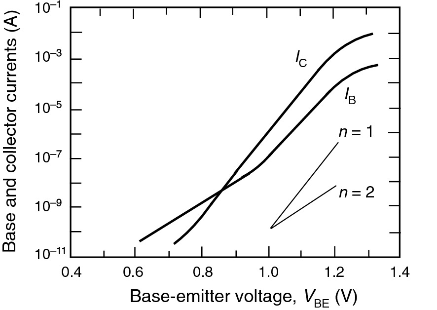
The current gain of a BJT and HBT is commonly measured using the Gummel plot scheme [14]. A Gummel plot shows the base and collector currents as functions of VBE when VCB = 0. The ratio of the measured IC/IB at various VBE gives the current gain. For the ideal case, both IB and IC are dominated by diffusion current component and proportional to exp(qVBE/kT). We expect a constant gain independent of bias. In real devices, defects and other recombination centers at the EB hetero-interface and in the bulk of the base lead to a non-ideal base current with an exp(qVBE/mkT) dependence. The parameter m is referred to as the ideality factor and has a value between 1 (dominated by diffusion current) and 2 (dominated by generation-and-recombination current Is). Therefore, the EB junction property can be determined by the ideality factor (m) of IB. For example, Fig. 9.39 shows the Gummel plot of an InGaP/GaAs DHBT with an emitter size of 60 × 60 µm2. At low current, m = 1.84 (~2), IB is mostly due to the generation-recombination current in the depletion region of the EB junction and Is is larger than Ir. At mid-to-high current, m = 1.15 (~1), showing that the bulk recombination current (Ir) in the base region becomes dominant due to its high doping level. The base current eventually departs from m ~ 1 due to the large voltage drops across the parasitic base and emitter resistances, causing the available junction voltage to decrease. For the collector current, it increases with VBE with an ideality factor of m = 1.07, a value which is close to unity.
../images/325043_1_En_9_Chapter/325043_1_En_9_Fig39_HTML.png
Fig. 9.39

Gummel plot for InGaP/GaAs HBT. The emitter size of the HBT is 60 × 60 µm2.

Reprinted with permission from [15], copyright IEEE

9.7.3 Band Discontinuity of Heterostructures
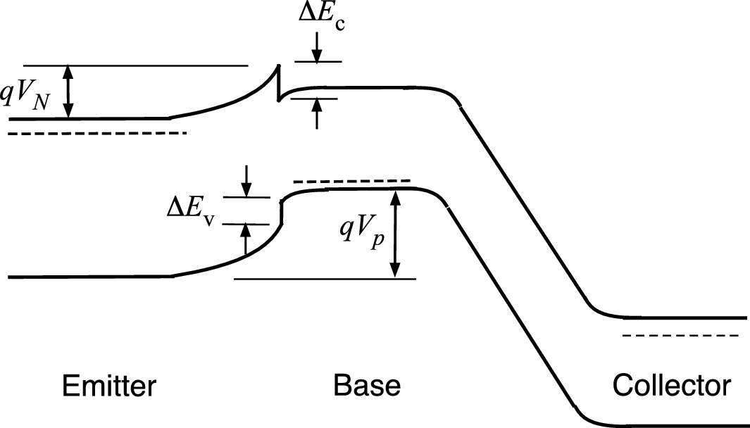
In a type-I heterostructure, a ‘spike-and-notch’ energy band diagram generally appears at the abrupt heterojunction due to the conduction band discontinuity ΔEc as shown in Fig. 9.40 for a SHBT. This energy spike can be removed by using a graded composition in the large bandgap emitter near the hetero-interface as used for discussions in the previous section. The existence of the energy spike at the EB junction of an abrupt HBT can modify the current conduction across the heterojunction. Using the simple thermionic emission model, the magnitude of forward current depends on the amount of electrons having enough energy to surmount the potential barrier. In an abrupt HBT, the potential barrier for electrons is simply VN. However, in a graded HBT, the effective potential barrier becomes (VN − ΔEc/q) since the energy spike, ΔEc, has been eliminated by the graded composition design. Therefore, under the same bias condition, the collector current of the abrupt HBT, In(abrupt), is reduced from the graded HBT, In(graded), by a factor of
../images/325043_1_En_9_Chapter/325043_1_En_9_Fig40_HTML.png
Fig. 9.40

Energy band diagram for HBT with abrupt emitter–base junction

$$ \frac{{I_{n} \left( {\text{abrupt}} \right)}}{{I_{n} \left( {\text{graded}} \right)}} = \frac{{\exp \left( { - qV_{N} / {kT}} \right)}}{{\exp \left[ { - \left( {qV_{N} -\Delta E_{\text{c}} } \right) / {kT}} \right]}} = \exp \left( { -\Delta E_{\text{c}} /{kT}} \right) $$
(9.79)
Since the current gain is proportional to exp(ΔEg/kT) in the graded junction case, the current gain of abrupt HBTs is modified by reducing ΔEc from ΔEg in the injection current relation (9.75). Thus
$$ \beta_{{\max} } = \frac{{N_{\text{E}} \upsilon_{{n{\text{B}}}} }}{{p_{\text{B}} \upsilon_{{p{\text{E}}}} }}\exp \left( {\frac{{\Delta E_{\text{g}} -\Delta E_{\text{c}} }}{kT}} \right) = \frac{{N_{\text{E}} \upsilon_{{n{\text{B}}}} }}{{p_{\text{B}} \upsilon_{\text{pE}} }}\exp \left( {\frac{{\Delta E_{\text{v}} }}{kT}} \right) $$
(9.80)

It is clear that a large ΔEv is preferred in abrupt N-p+-n HBT structures for a high current gain.

The existence of the energy spike in the conduction band at the EB heterojunction has other effects on device performance. A beneficial effect is that electrons injected from emitter into the base have to overcome the EB junction barrier with higher potential energy and become hot electrons with high saturation velocity. The improved travel speed across the base region leads to a reduced base transient time for high frequency operation. A detrimental effect is that the energy spike can block current flow at bias voltages VCE < ΔEc/q = Voff, which is the offset voltage. Also, the triangular QW formed on the base side of the EB junction can trap electrons that lead to an enhanced recombination at the junction. Therefore, the current gain will be reduced due to an increasing Ir.
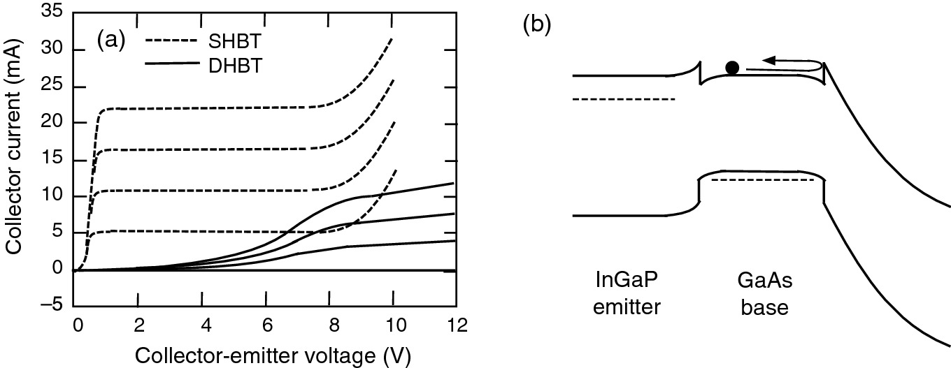
Next, we turn our attention to the BC junction. In a SHBT, the same semiconductor is used for both base and collector and the BC junction is a homojunction. Therefore, the same arguments about the BC junction of a BJT can be applied to a SHBT. In DHBTs, the BC homojunction is replaced with a heterojunction. The use of a wide bandgap collector material can improve the power handling capability by the enhanced breakdown voltage. Again, due to the existence of a finite ΔEc, an energy spike forms at the BC junction as shown in Fig. 9.41. This energy barrier (ΔEc) impedes free collection of electrons by the reverse-biased BC junction. It will suppress the collector current until a large VCE is reached to allow collection of electrons by the collector. Thus, it will increase the minority carrier resident time in the base region, which reduces the bandwidth of the device. Therefore, a graded collector junction in the form of composition grading or chirped superlattice structure is usually used to eliminate this problem. For a lattice-mismatched material system such as InGaAs/InP, this will complicate the growth procedures and may cause interface problems leading to a lower current gain.
../images/325043_1_En_9_Chapter/325043_1_En_9_Fig41_HTML.png
Fig. 9.41

a Comparison of the IV characteristics of InGaP/GaAs SHBT and DHBT. The base current was stepped from 0 to 400 µm in 100 µA steps. Reprinted with permission from [16], copyright AIP Publishing. b Current blocking at the base–collector junction of an InGaP/GaAs DHBT
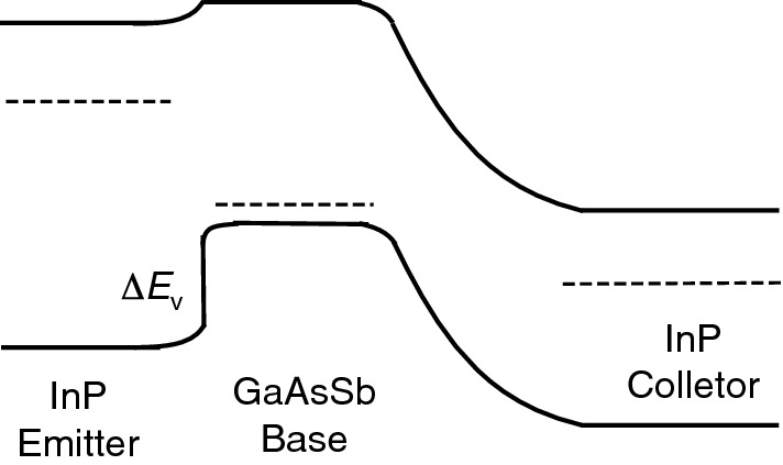
The collector current blocking mentioned above can be totally avoided by using a type-II DHBT design. This design simplifies the growth of the BC junction without using composition grading. In particular, for the InP/GaAs0.5Sb0.5/InP DHBT design shown in Fig. 9.42, it provides a nearly zero conduction band offsetEc = −0.06 eV, Ec(InP) < Ec(GaAsSb)) for a negligible turn-on voltage and no current blocking effect at the BC junction. The large ΔEv of ~0.62 eV and the use of InP collector material provide a large current gain and large breakdown voltage, respectively.
../images/325043_1_En_9_Chapter/325043_1_En_9_Fig42_HTML.png
Fig. 9.42

Energy band diagram of an InP/GaAsSb type-II double-heterojunction bipolar transistor

9.7.4 High-Frequency Operation of HBT

The high-frequency performance of HBTs is fundamentally determined by the stored minority carrier charge in the transistor that has to be removed from (added to) the transistor before it can turn off (on). Hence, the maximum frequency at which the transistor is capable of operating depends on the junction capacitance charging time and charge carrier transit time. In forward active operation, the forward transit time τF or the emitter-to-collector transit time τEC represents a fundamental limit for the switching speed and maximum frequency of operation of a HBT. The parameter most commonly used to define this maximum frequency of operation is the cutoff frequency fT. This is the frequency at which the common emitter, small-signal current gain drops to unity under conditions of a short-circuit load.

In practice, parasitic capacitance and resistance of the HBT will slow down the switching of digital circuits and limit the frequency of operation of analog circuits. To include the effect due to parasitic resistances and junction capacitances, the maximum oscillation frequency fmax is a good predictor of transistor performance.

  1. (a)

    Emitter-to-collector transit time

     
The emitter-to-collector transit time models the excess charge stored in the HBT under normal operation of a common-emitter configuration. This is an extremely important device parameter, since it sets a fundamental physical limit to the switching speed and maximum oscillation frequency of operation of a HBT. The emitter-to-collector transit time τEC can be written as the sum of the individual delay times as well as charging times of junction capacitances in the various regions of the HBT.
$$ \tau_{\text{EC}} = \tau_{\text{E}} + \tau_{\text{B}} + \tau_{\text{C}} + \tau_{\text{BC}} $$
(9.81)
where τE, τB, τC, and τBC are the emitter delay time, base transit time, collector transit time, and base–collector space-charge layer delay time, respectively. The emitter delay τE associates the emitter junction charging time involving the emitter–base junction capacitance CE and the dynamic emitter resistance kT/qIC.
$$ \tau_{\text{E}} = \frac{kT}{{qI_{\text{C}} }}C_{\text{E}} $$
(9.82)
The base delay τB represents the transport of electrons through the base layer via drift, diffusion, or ballistic transport. In the limit of diffusion current only,
$$ \tau_{\text{B}} \equiv \frac{{Q_{\text{B}} }}{{I_{\text{C}} }} $$
(9.83)
with
$$ \left\{ {\begin{array}{*{20}c} {Q_{\text{B}} = \displaystyle{\frac{{qAW_{\text{B}} n_{\text{B0}} }}{2}}\exp\left( {\frac{{qV_{\text{BE}} }}{{\it{kT}}}} \right) } \\ {I_{\text{C}} = qAD_{{n{\text{B}}}} \displaystyle{\frac{dn}{dx}} = qAD_{{n{\text{B}}}} \frac{{n_{\text{B0}} }}{{W_{\text{B}} }}\exp\left( {\frac{{qV_{\text{BE}} }}{{\it{kT}}}} \right)} \\ \end{array} } \right. $$
Thus,
$$ \tau_{\text{B}} = \frac{{W_{\text{B}}^{2} }}{{2D_{{n{\text{B}}}} }} $$
(9.84)
WB is the base width, DnB is the electron diffusion constant, and nB0 is the equilibrium electron concentration. This result of τB is valid for HBTs with a uniform base. If the base is non-uniformly doped or has a composition gradient, then the variation in doping and/or bandgap energy gives rise to a built-in electric field across the neutral base region. This built-in field would aid electron transport across the base and hence reduce the base transient time. This situation can be taken into account by modifying the equation as
$$ \tau_{\text{B}} = \frac{{W_{\text{B}}^{2} }}{{\gamma D_{{n{\text{B}}}} }} $$
(9.85)
where γ is a constant that has a value of 2 ≤ γ ≤ 4.
The collector transit time τC corresponds to the transport time through the collector layer, is classically found to be proportional to the collector thickness WC, and is expressed as
$$ \tau_{\text{C}} = \frac{{W_{\text{C}} }}{{2\upsilon_{\text{sat}} }} $$
(9.86)
where υsat is the electron saturation velocity in the collector, typically measured as 3–4 × 107 cm/s.
The last term τBC represents the charging time delay associated with the parasitic BC junction capacitance CBC. For an incremental input voltage change dVBE, the BC junction voltage change is
$$ {\text{d}}V_{\text{BC}} = {\text{d}}I_{\text{C}} \left( {R_{\text{C}} + R_{\text{E}} + {kT/}qI_{\text{C}} } \right) $$
(9.87)
where RC and RE are the parasitic collector and emitter resistances, respectively. Therefore,
$$ \tau_{\text{BC}} = \left( {R_{\text{C}} + R_{\text{E}} + {kT/}qI_{\text{C}} } \right)C_{\text{BC}} $$
(9.88)
The total delay associated with a HBT is directly related to the cutoff frequency and can be described as
$$ f_{\text{T}} = \frac{1}{{2\pi \tau_{\text{EC}} }} = \left\{ {2\pi \left[ {\tau_{\text{B}} + \tau_{\text{C}} + \left( {R_{\text{E}} + R_{\text{C}} } \right)C_{\text{BC}} + \frac{kT}{{qI_{\text{C}} }}\left( {C_{\text{E}} + C_{\text{BC}} } \right)} \right]} \right\}^{ - 1} $$
(9.89)
Since fT is defined for small-signal conditions, a small-signal circuit model, such as the hybrid-π model, as shown in Fig. 9.43, can be used to derive an expression for fT. To a first order, the series resistances of three terminals and recombination in the depletion region were neglected. Under the conditions of a short-circuit load, the small-signal collector and base currents can be written as
../images/325043_1_En_9_Chapter/325043_1_En_9_Fig43_HTML.png
Fig. 9.43

Small-signal hybrid-π circuit model of HBT

$$ i_{\text{c}} = {\text{g}}_{m} v_{\text{be}} - i\omega C_{\mu } v_{\text{be}} $$
(9.90)
$$ i_{\text{b}} = {\text{g}}_{\pi } v_{\text{be}} + i\omega \left( {C_{\mu } + C_{\pi } } \right)v_{\text{be}} $$
(9.91)
where gπ = 1/rπ (rπ is the equivalent input resistance), ω = 2πf, gm is the transconductance, Cπ is the BE junction diffusion capacitance, and Cµ is the BC junction diffusion capacitance.
The common-emitter current gain can be written as
$$ \beta = \frac{{i_{\text{c}} }}{{i_{\text{b}} }} = \frac{{{\text{g}}_{m} - i\omega C_{\mu } }}{{{\text{g}}_{\pi } + i\omega \left( {C_{\mu } + C_{\pi } } \right)}} \cong \frac{{{\text{g}}_{m} }}{{{\text{g}}_{\pi } + i\omega \left( {C_{\mu } + C_{\pi } } \right)}} $$
(9.92)
If we define β0 = gmrπ, the equation can be simplified as
$$ \beta = \frac{{\beta_{0} }}{{1 + i\omega r_{\pi } \left( {C_{\mu } + C_{\pi } } \right)}} $$
(9.93)
At low frequencies, the current gain maintains a constant value of β = β0. As the frequency increases, the second term in the denominator of the equation becomes large with respect to unity, and β can be approximated by
$$ \left| \beta \right| = \frac{{\beta_{0} }}{{2\pi fr_{\pi } \left( {C_{\mu } + C_{\pi } } \right)}} $$
(9.94)
At high frequencies, β begins to roll off with a limiting roll-off rate of −20 dB/decade (∝1/f). The frequency-dependent gain values are determined from S-parameters measured with microwave network analyzers. The gain values (in dB) as functions of frequency are usually plotted in a semi-log fashion under constant VCE = VBE and IC as shown in Fig. 9.44a. For very high-speed devices, the gain at frequencies exceeding the limit of instrument capacity was obtained by extrapolating −20 dB/decade lines from a best-fit average of the measured current gain.
../images/325043_1_En_9_Chapter/325043_1_En_9_Fig44_HTML.png
Fig. 9.44

a RF response and performance figure extrapolations for 0.25 × 16 µm2 InP/InGaAs SHBT. Reprinted with permission from [17], copyright IEEE. b fT and fmax as a function of collector current density of a 0.35 × 8 µm2 type-II InP/GaAsSb DHBT. Reprinted with permission from [18], copyright American Vacuum Society

Since τEC is a function of the collector current, the cutoff frequency is also a function of the collector current as illustrated in Fig. 9.44b. At low collector currents, the depletion capacitance term (τBC) in (9.89) dominates and hence fT increases with IC. At medium currents, the transit time terms become larger than the depletion capacitance term, and fT ceases to rise with collector current. At high collector currents, the cutoff frequency decreases markedly due to high current effects, especially the Kirk effect which will be described later.

The other important high-frequency parameter for a HBT is the maximum oscillation frequency fmax, where the unilateral power gain (U) drops to unity. The unilateral or Mason gain is the maximum gain obtained by conjugate matching of inputs and outputs of the device, together with the use of a lossless feedback network to tune out any internal device feedback. The derived expression of the maximum oscillation frequency is
$$ f_{ {\max} } = \sqrt {\frac{{f_{T} }}{{8\pi C_{BC} R_{B} }}} $$
(9.95)
which shows that the fmax is determined not only by the fT but also by BC junction capacitance CBC and the base resistance RB. It is clear that a high p-type doping concentration in the base region leads to a low base sheet resistance and an improved fT, both of which enhance the fmax. On the other hand, the increase in fT due to reduced τBC by higher collector doping could increase CBC and may cause a decrease in fmax, depending on the relative importance of τBC in fT. Therefore, for high-frequency circuit applications, a careful optimization of these two parasitics is required.
  1. (b)

    Kirk effect

     
The reduction of fT at high collector current mentioned in the last section is due to a base widening or Kirk effect. Consider Poisson’s equation in the depletion region of the BC junction:
$$ \frac{{{\text{d}}F}}{{{\text{d}}x}} = \frac{\rho }{\epsilon } = \frac{q}{\epsilon }\left( {p - n + N_{d} } \right) $$
(9.96)
where p and n are mobile charges and Nd is the fixed (ionized) charges. In the reverse-biased collector of N-p-n HBT structures, $$ p \approx 0 $$ and electrons injected from the emitter are transported across the BC junction by drift under high field situations. The electron concentration relates the drift current density Jn by n = Jn/sat, where υsat is the electron saturation velocity. Thus,
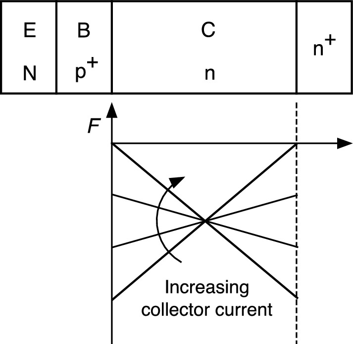
$$ \frac{{{\text{d}}F}}{{{\text{d}}x}} = \frac{1}{\epsilon }\left( {qN_{d} - \frac{{J_{n} }}{{\upsilon_{\text{sat}} }}} \right) $$
(9.97)
This equation indicates that the slope of the electric field intensity depends on the difference of qNd and Jn/υsat. Under low current density, the contribution from the mobile electrons can be neglected and dF/dx is unchanged (Fig. 9.45). At sufficiently large collector current density, the BC depletion region can extend all the way to the n/n+ subcollector boundary. For a fixed VCB, the depleted collector region where the electric field F exists is fixed and dF/dx still maintains a positive slope. With further increasing the collector current density (JC), the mobile charge in the depletion region becomes significant and cannot be neglected. This leads to a decreasing F with increasing JC or a decreasing dF/dx slope. At certain JC, F = 0 and the depleted collector layer turns into a neutral layer. Holes can be injected freely from the base into the adjacent neutral collector region. With the injected holes, the conductivity type of the collector adjacent to base changes from n to p. Thus, the effective base thickness is increased at high collector current density, which degrades the cutoff frequency of the HBT as shown in Fig. 9.44b.
../images/325043_1_En_9_Chapter/325043_1_En_9_Fig45_HTML.png
Fig. 9.45

Electric field intensity distribution in the fully depleted collector region under large collector current density. With further increase of collector current density, the slope of the electric field intensity curve changes from positive to negative as indicated by the arrow

  1. (c)

    Device scaling and surface passivation
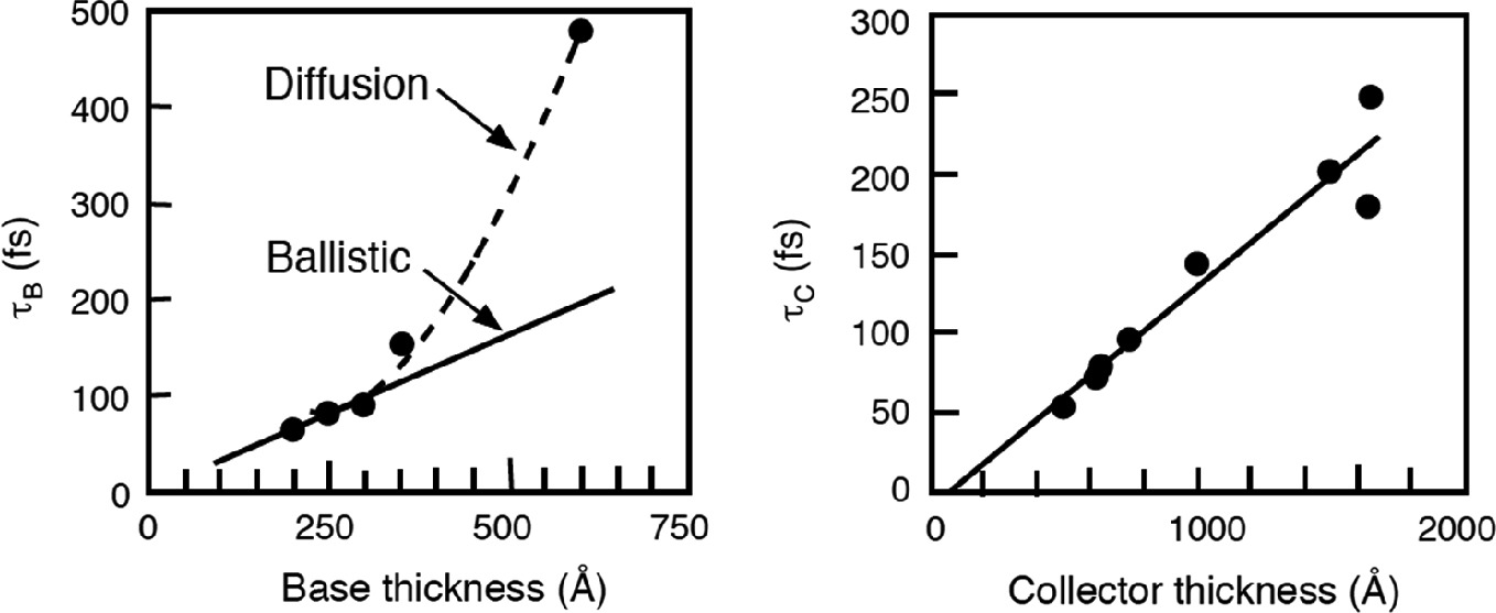
     
Earlier studies of HBTs have shown that a significant component (>75%) of the total device delay was associated with the intrinsic forward delay of the device, primarily the base and collector transit times. Therefore, an effective method to increase the cutoff frequency fT of the HBT is through vertical scaling of the base and collector epitaxial layers. Vertical scaling strictly involves the design of layer thicknesses, doping levels, and bandgap engineering to reduce device transit time, thereby increasing device bandwidth. Figure 9.46 shows the experimental relationship between vertical scaling and base/collector transit times. The base transit time is clearly illustrated by two slopes. For thicker bases, the classic diffusion transport dominates and is proportional to (WB)2. As the base thickness is scaled below the mean free path for electrons (~30 nm), the ballistic transport dominates with a linear dependence on WB. However, as the base and collector layers are thinned, parasitic resistances and capacitances also increase—specifically the base resistance, RB, and the base/collector capacitance, CBC. The increase of these parasitic components acts to severely degrade the maximum oscillation frequency fmax of the device.
../images/325043_1_En_9_Chapter/325043_1_En_9_Fig46_HTML.png
Fig. 9.46

Experimental results on the relationship between vertical scaling of InGaAs/InP SHBT and base/collector transit times
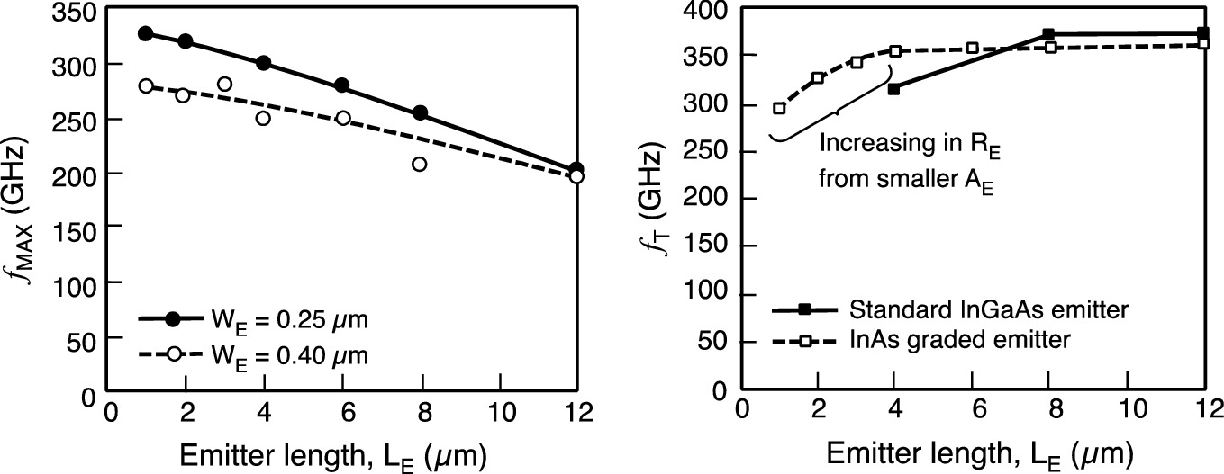
For effective reduction of transit times in HBTs without incurring significant increases in charging delays, vertical and lateral scaling must be simultaneously employed in order for submicron devices to achieve high performance. Lateral scaling refers to device topology design and processing techniques used to reduce parasitic capacitances and resistances to further enhance device speed. Lateral scaling also has the benefit of providing lower power operation and more efficient heat removal; reducing the emitter length lowers the thermal resistance of the HBT, allowing for higher current densities and lower junction temperatures. Figure 9.47 shows the peak fmax and fT values versus emitter dimensions of InP/InGaAs SHBTs. For the 0.25 µm emitter width (WE), a 76% improvement in fmax is observed from reducing emitter lengths (LE) from 12 µm to 1 µm; shrinking the emitter width from 0.4 µm to 0.25 µm results in an l8% fmax increase.
../images/325043_1_En_9_Chapter/325043_1_En_9_Fig47_HTML.png
Fig. 9.47

Experimental results on the relationship between emitter lateral scaling of InGaAs/InP SHBT and cutoff frequency

Beyond a certain point, however, scaling has detrimental effects on device performance due to physical limitations imposed by shrinking device dimensions. The significant drop in fT observed in Fig. 9.47 for emitter lengths 8 µm and smaller on a standard InGaAs emitter cap is attributed to an increase in emitter resistance due to smaller contact areas. Ideally, scaling theory predicts that fT should remain constant regardless of emitter length. However, the finite cap doping causes large increases in contact resistance for these emitter areas. The emitter cap cannot be doped higher due to solid solubility limits, but emitter contact resistance can be reduced through emitter cap engineering by using a narrow-bandgap cap material such as InAs. InAs provides a better contact material because of the smaller bandgap, higher doping capability, and higher thermal conductivity when compared to a standard InGaAs cap. The utilization of an InAs emitter cap is shown to reduce the emitter contact resistance by a factor of 2 in submicron HBT devices. The contact resistance reduction enhances the scalability of the emitter by allowing the emitter length to scale to dimensions smaller than 4 µm before the fT degradation occurs. Overall, lateral scaling is often dependent on process maturity, relying on advanced fabrication techniques to counteract the effects of vertical scaling on fmax. Therefore, for HBT development using a new material system, the best indication of the system’s potential is determined by the fT of the transistor. It is assumed that as the process matures, the power gain of the device will be increased through technological advances.
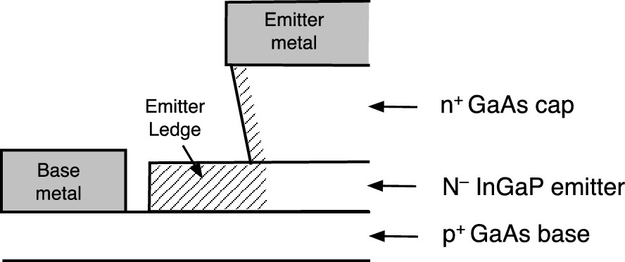
In general, the HBT has a vertical geometry with an intrinsic device size defined by the emitter contact area. The base contact is designed to surround the intrinsic base region underneath the emitter. Unavoidably, there is an exposed extrinsic base region between the base contact and the intrinsic base area. Consequently, in HBTs made of materials with a high surface recombination velocity (SRV), such as GaAs (SRV > 106 cm/s), some minority carriers injected from the emitter recombine with the base majority carriers on the exposed surfaces resulting in the extrinsic base surface recombination current. This base current component is proportional to the magnitude of the emitter periphery rather than the emitter area. As the size of the emitter is reduced, the emitter perimeter-to-area ratio increases and surface recombination current becomes a major part of the overall base current. The current gain of such a scaled down GaAs–base HBT is substantially reduced from that of a large device whose perimeter-to-area ratio is small. The surface recombination current problem can be reduced by passivating the exposed extrinsic base region that is not directly under the emitter with an emitter ledge as shown in Fig. 9.48. A thin ledge of emitter material left surrounding the emitter mesa can dramatically reduce surface recombination current and improve device scaling. The exposed ledge layer outside the emitter mesa is totally depleted, and no carriers are available for recombination at the surface. Therefore, the base current is not affected and current gain is preserved. On the other hand, the free InxGa1−xAs surface shows more ideal surface characteristics with a small SRV of 103 cm/s for an In composition x ~ 0.5. Therefore, for HBT materials with low SRV such as in InP/InGaAs HBTs, the surface recombination current is not significant even in small devices and the surface passivation is not required.
../images/325043_1_En_9_Chapter/325043_1_En_9_Fig48_HTML.png
Fig. 9.48

Cross-sectional drawing of a HBT with emitter ledge passivation. The emitter ledge (hatched area) is totally depleted such that the base current underneath is not affected

9.7.5 Basics of HBT Processing
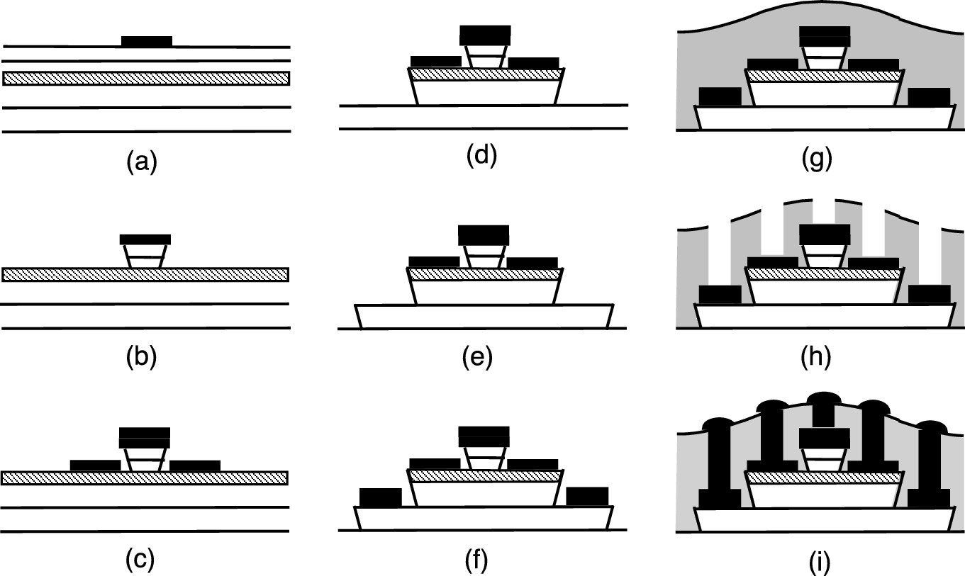
The design of HBTs is intimately interwoven with the technologies used for their fabrication. Therefore, any study of the HBT would be incomplete without understanding the fabrication technology. A typical HBT process developed at the University of Illinois at Urbana-Champaign (UIUC) is discussed below for either InGaP/GaAs or InP/InGaAs high-frequency HBTs. Other research groups may have developed their own HBT process steps, but the principal ideas discussed below remain the same. The standard InGaP/GaAs HBT structure is a single heterojunction device grown on a semi-insulating GaAs substrate that employs a carbon-doped GaAs base, a lattice-matched InGaP emitter, and a thin InGaAs emitter contact layer. Figure 9.49 shows a series of device profiles detailing the high-speed HBT process sequence. Initially, in Fig. 9.49a, non-alloyed metal contacts are deposited on the InGaAs emitter contacting layer. The cap and emitter material are then selectively chemically etched using the emitter metal as a mask, and this etch is followed by a selective InGaP emitter etch. This etching sequence provides an approximately 0.2 µm undercut beneath the emitter metal, which is necessary for the deposition of self-aligned, non-alloy base contact (Fig. 9.49c). After the base metallization, the base and collector are chemically etched, leaving the subcollector exposed (Fig. 9.49d). Before the collector metallization, an etch of approximately 1000 Å into the substrate is performed to electrically isolate the HBT (Fig. 9.49e). Next, the collector contacts are deposited on the collector mesa and overlap the edge of the isolation mesa (Fig. 9.49f). By allowing this overlap, the active collector contact area near the edges of the mesa is maximized and the collector contact resistance is reduced. The HBT device structure has now been defined. Figure 9.50a shows the scanning electron microscope (SEM) top-view micrograph of a fully fabricated single-finger GaAsSb/InP DHBT with an emitter size of 0.25 × 5 µm2.
../images/325043_1_En_9_Chapter/325043_1_En_9_Fig49_HTML.png
Fig. 9.49

Cross-sectional diagrams of UIUC HBT process: a post-emitter contact liftoff, b post-base etch, c post-base contact liftoff, d post-collector etch, e post-isolation etch, f post-collector contact liftoff, g post-polyimide/SiNx passivation, h post-SiNx via etch, and i post-overlay metal liftoff
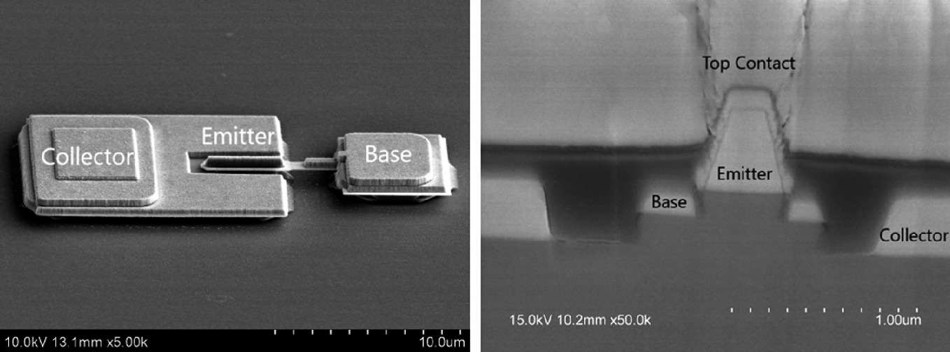
../images/325043_1_En_9_Chapter/325043_1_En_9_Fig50_HTML.png
Fig. 9.50

Left: Top view SEM micrograph of a fully fabricated GaAsSb/InP DHBT before planarization with an emitter size of 0.25 × 5 µm2. Right: Cross-sectional SEM micrograph of a completed GaAsSb/InP DHBT with an emitter size of 0.35 × 5 µm2.

Courtesy M. Feng, University of Illinois at Urbana-Champaign

At this point, the HBT has a non-planar topology. In order to make the HBT structure more planar to facilitate both via etching and the formation of planar probe pads for high-frequency testing, a planarization process (Fig. 9.49g) is required. The spin-on polyimide followed by a deposited Si3N4 layer completes the planarization process. Contact vias are defined using standard photolithography process (Fig. 9.49h). After the vias have been etched, a 1 µm layer of overlay metallization is deposited to form the probe pads and interconnect metallization. In the last step, an airbridge process is utilized to produce a second level of plated interconnect metallization allowing emitter fingers to connect to common-emitter probe pads. The cross-sectional SEM micrograph of a GaAsSb/InP DHBT with an emitter size of 0.35 × 5 µm2 is shown in Fig. 9.50b.

9.8 III–V Metal-Oxide-Semiconductor Field-Effect Transistors

Silicon metal-oxide-semiconductor field-effect transistor (MOSFET)-based integrated circuit (IC) technology is the dominant semiconductor technology used by all electronics industries with a 2018 worldwide sales of over $470 billion. Miniaturization of the feature size of ICs to increase the density of components has been the foundation of the over 50-year-long steady advance of silicon technology. Following Moore’s law, the exponential increase of transistor count per unit area as a function of time has been faithfully delivered by the industry since 1970. The minimum transistor gate length also decreases with time exponentially by incorporating strained SiGe channel material, high-κ gate dielectrics, and non-planar multigate structures (see Fig. 1.​4). Although 5-nm-node CMOS circuits are on the horizon, further reduction of the feature size to below 2 nm will push the device structure into the quantum regime. At that moment, the silicon technology will reach the point at which significant materials and device innovations will be required to further technology developments. One possible solution for the future is the hybrid material system in which silicon, germanium, and III–V compound semiconductors are integrated together on silicon wafers. For example, taking advantage of the very high electron mobility in GaInAs and high hole mobility in germanium, advanced CMOS circuits consisting of n-GaInAs channel and p-Ge channel MOSFETs might be fabricated together on the silicon wafer.

Because of their high bulk electron mobility, III–V MOSFETs have long been pursued in hopes of achieving performance superior to that of their Si counterpart. However, due to the high surface state density, the realization of unpinned surface Fermi level in III–V compound semiconductors had been elusive until two decades ago. In searching for a low defect density, thermodynamically stable gate dielectric, native oxide and deposited oxide using a variety of deposition techniques have been investigated. Unlike the SiO2/Si system, the native surface species in III–V materials are complicated. For example, the stable oxides of GaAs consist of As2O3, As2O5, Ga2O3, Ga2O, and GaAsO4 with different thermodynamic properties. Among all native oxides in this system, the As-oxides are the least stable while Ga2O3 is the most stable oxide. When the low-temperature-grown oxides are annealed at higher temperature, the composition of the oxide layer changes significantly. As temperature increases, the less stable As-oxides either evaporate away or are converted to the most stable oxide in the system (Ga2O3) along with elemental arsenic located at the interface. The pinning of the Fermi level at the GaAs-oxide interface has been unambiguously correlated with significant amounts of As2O3, As2O5, and elemental As present in native oxides. In order to fabricate functional III–V MOSFETs, it is necessary to completely remove the surface native oxide first before a stable and robust dielectric can be deposited. Thus, the successful development of III–V MOSFET technology relies strongly on the surface passivation and interface control technology.

9.8.1 III–V Alloy Surfaces and Semiconductor-Oxide-Metal Interfaces

The semiconductor surface state model was first proposed by John Bardeen in 1947 to explain the Fermi level pinning phenomenon at the metal–semiconductor (M–S) interface. It is assumed that the distribution of surface states becomes charge-neutral if the states are filled to a particular energy level, ϕ0 (above EV = 0), inside the forbidden gap. In the strong pinning limit, the metal Fermi level is pinned by the interface states at ϕ0. The pinning energy level ϕ0 is then the charge neutrality level of the interface states. Since then, two principal models, the intrinsic model of metal-induced gap states (MIGS) and the extrinsic model of defect states, have been developed. In the intrinsic case, a semiconductor in contact with a metal contains intrinsic states inside its band gap which are the evanescent tails of the metal wave function decaying into the semiconductor. These states are the dangling-bond states of the broken surface bonds of the semiconductor and called MIGS. On the other hand, in the extrinsic case, the interface states are introduced near the surface by processing-induced bond disorder (e.g., disorder caused by metal deposition, etching, or chemisorption of oxygen). In general, both types of interface states, MIGS and defects, could cause pinning. However, there is no universally accepted model for the M-S interface. Nevertheless, these studies of M-S contact have enriched our understanding of the chemistry and physics of III–V surfaces, such that III–V-oxide interface models can be developed.
  1. (a)

    Empirical CNL model of M-S interfaces


In semiconductors, the dangling-bond energy is typically located inside the band gap and the interface trap density (Dit) increases exponentially in the energy ranges close to the band edges. The Dit distribution forms a U-shaped continuum of donor- and acceptor-type states with its minimum, or the pinning energy, located at the charge neutrality level (CNL). The CNL energy level represents a weighted average value over the density of states. CNL is pushed away by the large DOS of the conduction and valence bands from the intrinsic energy level Ei, as shown in Fig. 4.​21. Therefore, the semiconductor surface pinning energy CNL is located inside the forbidden gap for most semiconductors. If the Fermi level EF is above CNL, the states are of acceptor type and negatively charged if the states are occupied. If the Fermi level EF is below CNL, the states are of donor type and positively charged if the states are occupied.
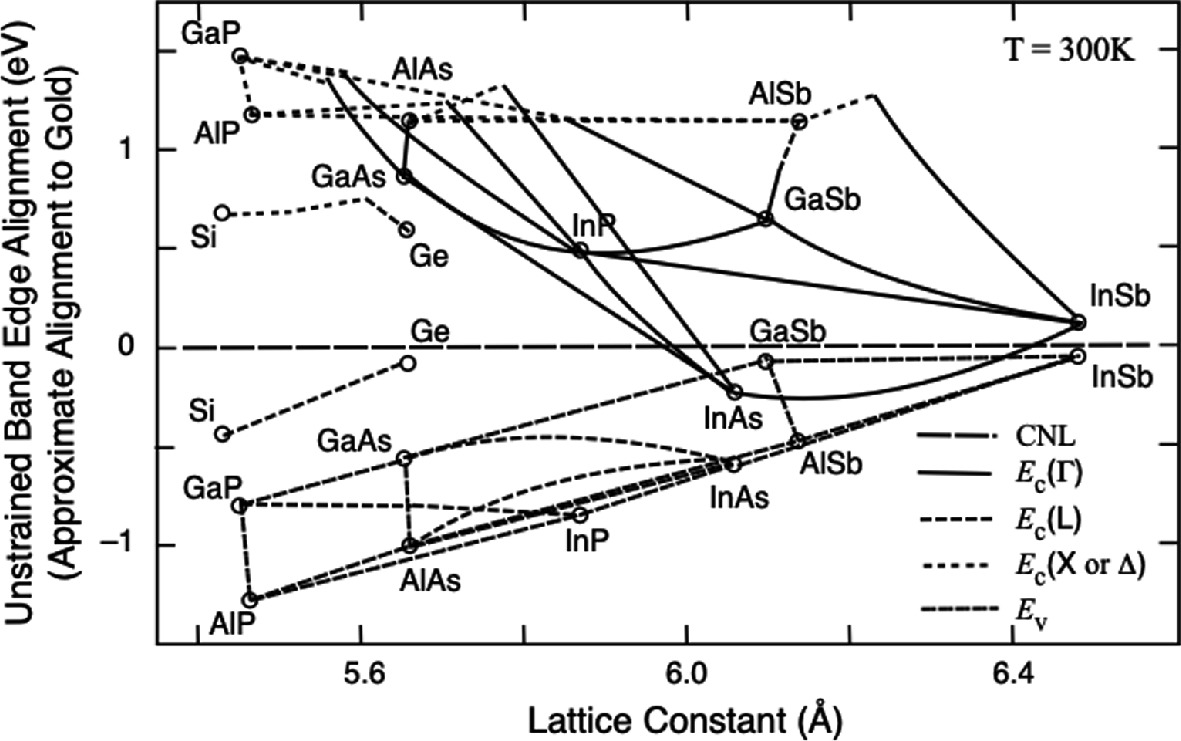
The CNL energies can be calculated from their pseudopotential band structures. The CNL values (above Ev = 0) of III–V binaries are determined by averaging values derived from various theoretical models as shown in Table 4.​5. The experimental CNL values of the semiconductors can be extracted from Schottky barrier heights. In general, the calculated CNL is in close agreement with Schottky barrier heights (ϕbv) on p-type III–V binary compounds. Thus, one can determine the surface pinning energy of III–V binary and ternary compound semiconductors empirically based on the valence band alignment method developed by S. Tiwari and D. J. Frank (Sect. 6.​1). Figure 9.51 shows the complete room-temperature conduction band-edge and valence band-edge energies as a function of the lattice constant for unstrained III–V compound semiconductors. This is the same figure that Tiwari and Frank derived (Fig. 6.​5) for band discontinuity determination except the zero point of the energy is now representing the charge neutrality level (CNL) or trap neutral level (ϕ0) for each lattice constant group. In the case of Si, the state-of-the-art SiO2/Si interface has very low interface trap density of 109–1010/cm2−eV. Although the energy separation between CNL is ~0.6 eV and ~0.5 eV from the conduction band minimum (CBM) and valence band maximum (VBM), respectively, the Fermi level is unpinned. Thus, high-performance n-MOSFETs and p-MOSFETs are routinely fabricated. In the case of GaAs, CNL is far away from CBM (~0.8 eV) and VBM (~0.6 eV) so that both GaAs n-MOSFET and p-MOSFET are difficult to realize when significant interface traps presented. It is interesting to note that CNL is inside the conduction band of InAs. This indicates that InAs-based n-MOSFETs are easy to realize. For example, T. Brody and H. Kunig, in 1966, demonstrated both enhancement- and depletion-mode MOSFETs using evaporated SiO2 on InAs film prepared by co-evaporation method. One interesting ternary system is InGaAs where the CBM of In-rich InGaAs intersects CNL at xInAs ~ 0.75. Thus, In-rich InGaAs n-MOSFET is relatively easy to achieve.
../images/325043_1_En_9_Chapter/325043_1_En_9_Fig51_HTML.png
Fig. 9.51

Energy alignment of CNL with the band edges of elemental and III–V semiconductors at MOS interfaces plotted as a function of the lattice constant of semiconductors. For III–V compounds, the circles indicate the band edges of binaries and the lines show the band edges of ternaries
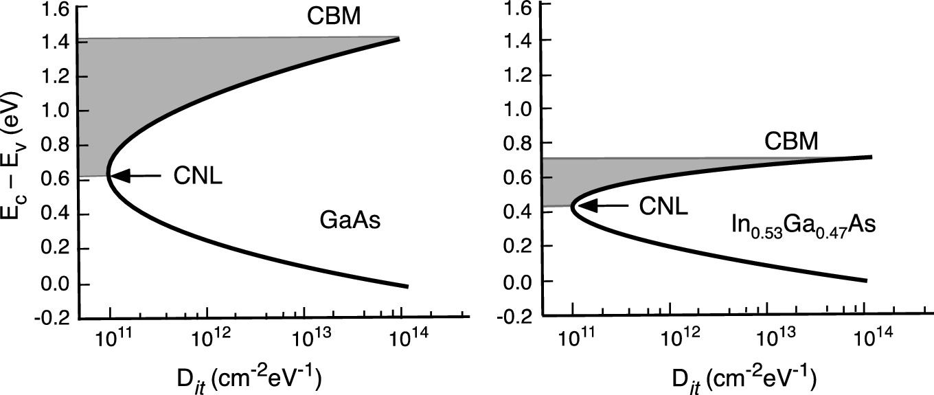
For device applications, the next important issue after unpinning the Fermi level is achieving strong electron inversion in III–V MOSFETs. This can be explained using the distribution of the density of the surface states Dit as a function of the energy as shown in Fig. 9.52. It is assumed that the Dit distribution from VBM to CBM (with energy ECBM) is nearly parabolic in a logarithmic scale due to the significant interface traps at III–V interfaces. The minimum value of Dit depends on the surface processing techniques. For simplicity, the Dit value at CBM is fixed at 1014 cm2−eV for all III–V compounds and has a minimum value located at CNL (with energy ECNL). Assuming the strong electron inversion occurs when the Fermi level reaches CBM, the number of interface-trapped negative charges Qit can be calculated by integrating Dit from ECNL to ECBM. It is obvious that the dominant factor is the energy difference between ECNL and ECBM. The built-in negative charges Qit to prevent a strong inversion charge to participate in transport are larger for the material with a deep CNL below CBM. For example, in GaAs, with the CNL located ~0.8 eV below CBM, it builds up ~10−6 C/cm2 negative charges to prevent a strong inversion charge to participate in transport. In contrast, the CNL and CBM potential difference for In0.53Ga0.47As lattice-matched with InP is only 0.27 eV. The built-up negative charge is only ~3.4 × 10−7 C/cm2, a factor of three smaller than that in GaAs. Therefore, it is much easier to realize an inversion-mode In0.53Ga0.47As/InP MOSFET than a GaAs MOSFET.
../images/325043_1_En_9_Chapter/325043_1_En_9_Fig52_HTML.png
Fig. 9.52

Schematic for the parabolic Dit distribution within energy band of GaAs and In0.53Ga0.47As. The CNL is aligned 0.8 eV and 0.27 eV below CBM for GaAs and In0.53Ga0.47As, respectively. The shaded area shows the built-up negative charges in interface traps after Fermi level moves from CNL to CBM.

Reprinted with permission from [19], copyright AIP Publishing

  1. (b)

    High-κ dielectrics and oxide-semiconductor (O-S) interfaces

     
Scaling of the silicon complementary metal-oxide-semiconductor (CMOS) FET technology is at the center of Moore’s law. The exponential increase of transistor count per unit area as a function of time has been faithfully delivered by the industry since 1970. The minimum transistor gate length also decreases with time exponentially. However, when the feature size is reduced to below 65 nm, the SiO2 gate dielectric layer becomes so thin (<2 nm) that the gate leakage current due to direct tunneling of electrons through SiO2 becomes very high. The excessively large leakage current leads to an unacceptably high circuit power dissipation level. The FET is a capacitance-coupled device, where the source–drain current of the device depends on the gate capacitance,
$$ C = \epsilon_{0} \kappa A /t $$
(9.98)
where $$ \epsilon_{0} $$ is the permittivity of free space, κ is the relative permittivity (dielectric constant), A is the area, and t is the thickness of the dielectric SiO2. Since the tunneling current decreases exponentially with increasing the dielectric thickness, a new dielectric with a larger dielectric constant than that of SiO2 (κ = 3.9) has to be introduced while maintaining the same capacitance. These non-native new gate oxides are called high-κ dielectrics. In selecting suitable high-κ dielectrics for microelectronics applications, there are several important requirements about their physical properties. First, the κ value must be high enough that it will be used for a reasonable number of years of scaling. A value of κ ≥ 20 is preferred. Second, the oxide must have large bandgap energy and act as an insulator, by having oxide-Si band offsets over 1 eV to minimize leakage current. Third, the oxide must be thermodynamically as well as kinetically stable such that it is compatible with extreme processing conditions. Above all, the selected oxide must form a good electrical interface with the semiconductor, which is dependent on the deposition method. The oxides that satisfy most of these criteria are Al2O3, HfO2, ZrO2, Y2O3, La2O3, and various lanthanides (e.g., Gd2O3).
For III–V MOSFETs, due to the lack of high-quality native oxides, high-κ dielectrics used in current Si technology are implemented as gate oxides. In order to use these dielectrics as the gate oxide of III–V MOSFETs, the conduction band (CB) offset, ΔEC, between the dielectric and III–V alloy must be over 1 eV to achieve a low leakage current. The CB offset at the M-S interface has previously been determined by the MIGS method using CNL as a reference energy level. The MIGS model is extended to determine band offsets between oxides and semiconductors. The CB offset is given by
$$ \Delta E_{\text{c}} = \left( {\chi_{\text{o}} -\Phi _{{{\text{CNL}},{\text{o}}}} } \right) - \left( {\chi_{\text{s}} -\Phi _{{{\text{CNL}},{\text{s}}}} } \right) + S\left( {\Phi _{{{\text{CNL}},{\text{o}}}} -\Phi _{{{\text{CNL}},{\text{s}}}} } \right) $$
(9.99)
Here ΦCNL is the charge neutrality level measured from the vacuum level, χ is the electron affinity (EA), and the subscripts o and s represent the oxide and semiconductor, respectively. S is a dimensionless pinning parameter where S = 1 describes the Schottky limit of no pinning and S = 0 describes the Bardeen limit of strong pinning. Empirically, S depends only on the optical dielectric constant of the oxide, $$ \epsilon_{\infty } $$, and follows the trend
$$ S = \frac{1}{{1 + 0.1\left( {\epsilon_{\infty } - 1} \right)^{2} }} $$
(9.100)
The CNL energies for high-κ oxides have been derived from the bands calculated by either the tight-binding or pseudopotential method. The calculated CNL energies (above the valence band edge) and measured bandgap energies, electron affinity, and optical dielectric constants of these high-κ oxides are listed in Table 9.3. The calculated band offsets of various high-κ oxides on III–V semiconductors are listed in Table 9.4. Most of these high-κ oxides deposited on III–V semiconductors have a large enough (>1 eV) conduction band offset for MOSFET applications.
Table 9.3

Experimental bandgap energy (Eg), dielectric constant (κ), electron affinity (EA), and optical dielectric constants ($$ \epsilon_{\infty } $$) of various high-κ oxides along with the calculated charge neutrality level energy above the valence band edge (ECNL) [2022]


Eg (eV)

κ

ECNL (eV)

EA (eV)

$$ \epsilon_{\infty } $$

a-Al2O3

6.3

7.5 [21]

3.2

3

3.2

HfO2

6

25

3.7

2.2

4

ZrO2

5.8

25

3.6

2.4

4.8

Y2O3

5.7

15

2.4

1.84

4.4

La2O3

6.0

30

2.4

1.9

4

Gd2O3

6

10 [22]

2.4

2.5

3.8

Table 9.4

Calculated conduction band offsetsEc, in eV) of various high-κ oxides on III–V semiconductors [20]


Al2O3

HfO2

ZrO2

Y2O3

La2O3

Gd2O3

GaP

0.67

0.77

0.73

1.65

1.65

1.2

InP

1.7

1.72

1.64

2.6

2.6

2.1

AlAs

0.97

1.05

1.0

1.9

1.9

1.5

GaAs

1.46

1.52

1.42

2.4

2.4

1.9

InAs

2.38

2.54

2.44

3.4

3.4

2.9

GaSb

1.50

1.58

1.53

2.46

2.46

2.0

InSb

2.08

2.18

2.14

3.06

3.06

2.62

GaN

0.86

1.15

1.08

2.02

2.02

1.57

9.8.2 Atomic Layer Deposition (ALD)

Atomic layer deposition (ALD) is a vapor-phase film growth method used to deposit ultra-thin, uniform, conformal, and pinhole-free films onto a substrate. It was invented in the 1970s for the production of large-area flat-panel displays. Strong interest in ALD by the semiconductor industry began in the mid-1990s stemming from the need for non-native oxides for continuous scaling of Si MOSFET devices. In 2007, Intel successfully integrated an ALD Hf-based high-κ dielectric process into its 45-nm-node mass production technology. In the meantime, efforts to find non-native oxides on GaAs with low interfacial states density have found a solution in UHV deposition of amorphous Ga2O3(Gd2O3) and single-crystal Gd2O3 on GaAs surface. After this breakthrough in material science, both depletion-mode and enhancement-mode GaAs MOSFETs were demonstrated using Ga2O3(Gd2O3) as a gate dielectric along with an ion implantation process. The investigation of ALD high-κ Al2O3 and HfO2 on GaAs and other III–V materials for the fabrication of III–V-based MOSFETs started in 2001 at Bell Labs. Soon after in 2003, GaAs MOSFETs with ALD Al2O3 gate dielectric were successfully demonstrated. Since then, the research of ALD high-κ dielectrics on III–V substrates has been extended to other material systems including InxGa1−xAs, InP, InSb, GaSb, and GaN.
  1. (a)

    Principles of ALD

     
An ideal ALD process consists of exposing the substrate surface alternatively to different precursors in a cyclic manner. It differs from CVD technique by keeping the precursors strictly separated from each other in the gas phase. As shown in Fig. 9.53, the process of one ALD growth cycle involves exposure of the substrate surface to alternating precursors A and B introduced sequentially without overlapping. In each alternate precursor pulse, the precursor molecules fully react with the surface in a self-limiting fashion that leaves no more than one monolayer (ML) at the surface. This ensures that the chemisorption reaction stops once all of the reactive sites on the substrate have been occupied. This automatic control of the amount of material deposited is a key feature of ALD. After terminating the pulse of precursor A, an inert gas (typically N2 or Ar) purge follows to remove the excess of unreacted precursor and gaseous by-products. The second precursor B is then introduced following an inert gas purge to complete one reaction cycle. It should be noticed that only in an ideal case is a monolayer of desired material formed per each reaction cycle. In practice, the material thickness is determined by the nature of the precursor-surface interaction and only a fraction of a monolayer is formed. The ALD cycle can be performed multiple times to increase the film thickness.
../images/325043_1_En_9_Chapter/325043_1_En_9_Fig53_HTML.png
Fig. 9.53

Schematic representation of an ALD growth cycle leading to the formation of a binary dielectric film using self-limiting surface chemistry. a Precursor A is pulsed and reacts with surface, b excess precursor and reaction by-products are purged with inert carrier gas, c precursor B is pulsed and reacts with surface, and d excess precursor and reaction by-products are purged with inert carrier gas. Above procedures are repeated until the desired material thickness is achieved

Typically, the process of ALD is performed at relatively low temperatures (<350 °C). The temperature range, where thin film growth proceeds by the irreversible and saturating surface control in an ALD mode, is referred to as the ‘ALD-window. Within this ALD-window, the deposition rate per cycle is a constant independent of the growth temperature. The process outside the ALD-window, however, generally results in non-ALD-type deposition due to precursor condensation or insufficient reactivity at low temperatures, and precursor thermal decomposition or rapid precursor desorption at high temperatures. Thus, it is necessary to carry out each deposition process within the designated ALD-window.

The main advantages of ALD are derived from the self-limiting and sequential deposition process. First, ALD offers an accurate and simple thickness control by utilizing saturating, irreversible reactions where the film thickness can be tailored by the number of growth cycles. Secondly, ALD provides excellent conformality over large and/or complex-shaped substrates of high aspect ratio and three-dimensionally structured materials. This is made possible by self-limiting, irreversible reactions that provide the same amount of material adsorbed on different parts of substrates. Furthermore, due to the self-limiting reaction nature of ALD, there is no need to control the reactant flux homogeneity and the deposition temperature dependence is weak. A wide range of materials can be deposited using ALD, including oxides, metals, and semiconductors, and there is a wide range of properties that these films can exhibit, depending on the application. However, due to its sequential monolayer deposition nature, ALD suffers from slow deposition rates.
  1. (b)

    ALD of high-κ dielectrics on III–V surfaces


Since 2007, the Si semiconductor industry has adopted ALD to integrate non-native oxides, e.g., HfO2-based high-κ dielectric, into its IC mass production lines to advance the technology node beyond 45 nm. Next, at the 22 nm node, a three-dimensional fin field-effect transistor (FinFET) structure is developed. In a FinFET, the fin-shaped gate with a high aspect ratio protruding above the bulk surface needs to be covered with a gate oxide of high compositional and thickness uniformity. This is a task tailored for the conformal ALD process. To further improve the device performance with higher speed and reduced power, it is necessary to look toward alternative semiconductors with higher carrier mobility, such as III–V semiconductors.

For non-native oxide deposited on III–V substrate surface using ALD process, the achieved interface state density is primarily decided by the precursor characteristics and surface preparation of the substrate surface. There are some general requirements for a suitable ALD precursor which include: (a) sufficient volatility but no self-decomposition at the deposition temperature (b) adsorption to the surface sites without etching the substrate, and (c) sufficient reactivity toward the second precursor. The metal precursors used in ALD on III–V surfaces can be divided into two groups, inorganic and organometallic. Halides are the most common inorganic precursors used for both CVD and ALD processes. Chlorides, a kind of halides, are reactive, stable at a broad temperature range, and available for many metals including AlCl3 and HfCl4. However, the deposited film may suffer from high residual chlorine and hydrogen content. On the other hand, alkyls, such as trimethyl aluminum (TMA), are ideal metalorganic precursors containing a direct metal carbon bond. They are highly volatile and very reactive with water through hydrolysis. Other metal precursors including the chelation of C (β-diketronates), O (cyclopendienyls), and N (amidinates) with alkyls to a metal have also been used. The variety in non-metal reactants is rather less than in metal reactants. Water, due to its high stability and reactivity in a broad temperature range, is the most commonly used oxygen source providing a hydroxyl-terminated surface in metal oxide ALD. Ozone is often used for deposition of oxides from metal precursors having bulky ligands that are not reactive with water. However, due to its strong oxidation power, there are potential concerns regarding undesirable surface oxide formation on the substrate by prolonged ozone exposures.

The other important factor that influences the quality of non-native oxide/III–V interfaces is the pre-cleaning or surface passivation of the substrate before ALD. Unlike the SiO2/Si material system, the III–V substrates lack a high-quality, natural insulator. Instead, a number of different native surface species including Ga–O bonds, In-O bonds, As–O bonds, and other III–V–O bonds are readily formed on III–V surfaces when exposed to ambient environment. To achieve a low interface state density on III–V surfaces, these oxides must be removed as much as possible before depositing high-κ dielectrics. Currently, a number of ex situ surface treatments of III–V (100) surfaces have been developed. The use of wet chemical treatment by soaking samples in NH4OH (29%) solution has been found to be effective in removing higher-oxidation states of As and Ga oxides. To prevent re-oxidation of the III–V surface after the etch, the sample can be further protected by monolayers of sulfur using a (NH4)2S treatment before loading into the ALD system. The sulfur is then blown off from the III–V surface during the temperature ramp-up in the ALD system. The key to cleaning up As-oxide and providing high-quality III–V/high-κ interfaces is the self-cleaning effect of the ALD process as described in the following section. However, the removal of Ga oxides by the ALD process is incomplete. Further detailed studies examining Al2O3 and HfO2 deposition on GaAs by ALD indicated that the efficiency of surface oxides removal is affected by the ALD precursors used. An ~1 nm interfacial layer containing significant Ga2O content was observed at the Al2O3/III–V interface deposited using TMA/water precursors, while a thicker interfacial layer (~2.5 nm) was observed from the HfO2 deposition using HfCl4/water precursors. The enhanced reactivity of Al(CH3)3 compared to HfCl4 is responsible for this difference.

Currently, Al2O3, HfO2, and their alloys constitute the major ALD dielectrics studied on III–V substrates. Other metal oxides including Gd2O3, La2O3, and Y2O3 have also been studied. The best achieved interface state densities (Dit) are between 1011 and low-1012/cm2eV, which are orders of magnitude higher than that of (Gd2O3)Ga2O3/GaAs deposited by in situ UHV MBE deposition (~5 × 10¹⁰/cm2eV) and far worse than the ideal SiO2/Si system (~109–1010/cm2eV). However, these interface state density values have already been improved significantly to allow the demonstration of inversion-mode MOSFETs on different III–V substrates. To further improve the technology, additional ALD metal oxides need to be developed for gate dielectrics of III–V substrates. Surface passivation methods before ALD require further refinement to achieve the right surface conditions including the formation of particular species of interfacial oxides. Furthermore, to make high-κ dielectric/III–V a manufacturable III–V CMOS technology, it is also necessary to avoid surface and interfacial defect formation in every step of device fabrication.

9.8.3 Oxides Deposition on III–V Substrates

  1. (a)

    Substrate surface preparation


In the process of fabricating III–V-based MOSFETs, the preparation of a suitable surface condition of the semiconductor substrate for oxide deposition is the most critical step. In the ideal case, the surface of III–V semiconductors is a perfect, flat, and homogeneous surface. In reality, the atomic bonds in the terminated plane are sheared off to become unsatisfied dangling bonds. These dangling bonds are fairly susceptible to chemical reactions with atmospheric gases leading to the formation of moderately thick native oxides and carbonaceous adsorbents. These native surface species including, e.g., Ga–O bonds, As–O bonds, elemental As, and As and Ga anti-sites on GaAs, are the culprits of the Fermi level pinning. Thus, it is very important to remove these native oxides and carbonaceous adsorbents on air-exposed III–V substrates such that further surface treatment or ‘passivation’ of the surface can be carried out before the deposition of high-κ dielectrics.

On the other hand, under the UHV conditions, in a clean surface without atmospheric gas contamination, those unpaired electrons of dangling bonds tend to form covalent bonds between adjacent atoms in a process termed ‘dimerization.’ These surface dimmers have a tendency to form highly ordered rows in order to minimize the free energy of the surface. Using reflection high-energy electron diffraction (RHEED) technique, the observed reconstructed surface structures of GaAs vary from Ga-rich (4 × 2) reconstruction through As-rich (2 × 4) reconstruction depending on the substrate temperature and the As-to-Ga beam flux ratio. The As-rich (2 × 4) surface is terminated with As dimers aligned along the [$$ \bar{1} $$10] direction, while the Ga-rich (4 × 2) surface has Ga dimers aligned along the [$$ \bar{1}\bar{1}0 $$] direction. Due to the high diffusivity of surface Ga atoms, prolonged exposure of the GaAs surface under high temperature and low As flux promotes the island formation leading to uneven morphology on Ga-rich GaAs surface. In contrast, the As-rich (2 × 4) surface, obtained under medium (~550 to 600 °C) temperature and As-beam flux conditions, provides a smooth surface. Since the FETs are surface devices, for in situ deposition of oxides under UHV conditions, the As-rich (2 × 4) surface is the one most relevant for MOSFET applications.
  1. (b)

    Surface passivation and oxide deposition


Over the past five decades, persistent efforts have been carried out in searching for surface treatment methods to passivate III–V surfaces such that MOSFETs can be demonstrated. However, the conventional practice of thermal, anodic, and plasma oxidation methods failed to achieve this goal. Using an in situ deposition approach, the first successful passivation of GaAs surface was demonstrated in 1995 by Minghwei Hong et al. at Bell Labs [23]. In this method, electron-beam evaporated Ga2O3(Gd2O3) [GGO] dielectric film was deposited on an MBE-grown wafer in a UHV connected multiple chamber system. During the experiment, the freshly grown GaAs with an As-stabilized (2 × 4) surface was transferred under UHV condition from the III–V MBE chamber to another chamber for oxide deposition. Prior to deposition, the GaAs surface stoichiometry and atomic order were preserved, as monitored using RHEED, with extremely low oxygen exposure. Then the GGO film was deposited on the clean, atomically ordered (100) GaAs surface at substrate temperatures below 600 °C to avoid chemical reactions with GaAs substrates. The oxide molecules were supplied by electron-beam evaporation of a single-crystal Gd3Ga5O12 source. MOS structures on GaAs with a low Dit on the order of mid 1010 cm−2 eV−1 were demonstrated for the first time. However, low Dit values were not obtained in other oxide/GaAs systems using Al2O3, SiO2, and MgO prepared by a similar approach. Furthermore, pure Ga2O3 films cannot passivate GaAs surfaces effectively and show very high leakage current with poorly defined breakdown characteristics.

Further studies indicated that the unpinning of the GaAs Fermi level using electron-beam evaporated GGO dielectric film results from the Gd2O3 epilayer restoring the surface As and Ga atoms to near-bulk charge. An understanding of the bonding between Gd2O3 and GaAs is important for the development of new dielectrics used in III–V-based MOSFETs. Based on the consideration of Gibbs free energies of formation of all possible pairs in Ga, As, Gd, and O, the growth initiates from bonding a layer of oxygen atoms to Ga (Ga2O3: −998 kJ/mole) by taking up the As site (GaAs: −70 kJ/mole) in GaAs structure. Then the oxygen atoms would proceed to bind to Gd atoms of the next row due to the very large Gibbs energy for Gd2O3 formation (−1739 kJ/mole). Thus, the initial growth of GGO on GaAs contains only Gd2O3, despite the fact that incoming fluxes consist of various other species including Ga2O3. In addition, this Gd2O3 film is grown in a single-crystal form on GaAs. The Gd2O3 film has a cubic structure isomorphic to Mn2O3 and is (110)-oriented in single domain on the (100) GaAs surface. Once a Gd2O3/GaAs interface is formed, however, the competition for oxygen is significantly reduced and inclusion of Ga2O3 becomes possible, resulting in an oxide mixture of Gd2O3 and Ga2O3. Thus, the high interface quality GGO/GaAs heterostructure consists of a transition from a single-crystal GaAs substrate, to an epitaxial coherent Gd2O3 oxide layer of two to three monolayers in thickness, and then to the amorphous mixed oxides. This result matches well with the model of high-quality SiO2/Si interface, where the crystalline-Si to amorphous-SiO2 transformation takes place via an ordered crystalline oxide layer ~5 Å thick. The in situ UHV deposition of Gd2O3 approach can be extended to other rare earth oxides due to their chemical similarity. For example, using Y2O3 as the high-κ dielectric, low trap densities of (3 − 5) × 1011 eV−1cm−2 have been achieved at the Y2O3/GaAs (001) interface. Similar to Gd2O3, the Y2O3 film is also grown in a single-crystal form on GaAs with Y2O3 (110) planes parallel to GaAs (001) planes.

In contrast to the in situ deposition approach, MOSFETs were also successfully demonstrated in 2003 using ex situ ALD high-κ Al2O3 films as the gate dielectrics on GaAs and other III–V materials. Metalorganic trimethyl aluminum and water were used as the metal precursor and oxygen source for the ALD process, respectively. Since the ALD process was conducted on the GaAs surface exposed to the ambient air after epitaxial growth, a thin native oxide layer consisting of Ga and As oxides as well as spurious organic contamination is formed on the GaAs surface. To achieve a low interface state density on III–V surfaces, these oxides must be removed as much as possible before depositing high-κ dielectrics. Currently, a number of ex situ surface treatments of III–V (100) surfaces using a combination of wet chemical etch in NH4OH (29%) solution and (NH4)2S treatment before loading into the ALD system have been developed as outlined in the previous section. The self-cleaning effect of the ALD process further cleans up the As-oxide and provides high-quality III–V/high-κ interfaces. For selected ALD precursors, the detailed process parameters are mainly decided by the precursor characteristics such as decomposition behavior, sticking coefficient, vapor pressure, etc. So far, a number of suitable metal precursors have been reported for ALD deposition of high-κ dielectrics on various III–V surfaces with Al2O3, HfO2, and their alloys constitute the most studied systems.
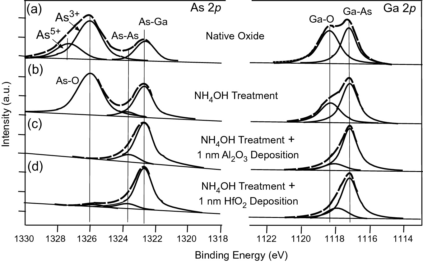
To understand interface passivation on III–V surfaces by ALD requires the knowledge of the surface oxides likely to be present on the surface in the course of device fabrication. In situ film deposition and analysis of the chemical state of the oxide interface can give a clear picture of the detailed reactions. An example of interface reactions of Al2O3 and HfO2 ALD processes on the NH4OH-treated GaAs surface using in situ X-ray photoelectron spectroscopy (XPS) is shown in Fig. 9.54. The air-exposed starting material is covered with native Ga and As oxides and excess As. The As 2p spectra show two As oxidation states, As3+ and As5+, corresponding to As2O3 and As2O5, respectively. The Ga–O signal of the Ga 2p spectra has multiple oxidation states including Ga3+ and Ga5+ as well as other oxide species. It is noted that the weaker bonded, higher-oxidation As states, e.g., As2O5 or As5+ states, are removed completely by wet NH4OH-treatment, leaving behind As3+ oxidation As states, reduced GaOx species as well as As–As bonding. The reduction of the As3+ oxidation state occurs during the TMA precursor pulse, whereby the Al3+ in the TMA precursor more efficiently replaces the As in the As3+ oxidation state, resulting in AlOx formation and presumably volatile As(CH3)3 reaction products. However, the reaction with As3+ oxidation state is less efficient for Hf originating from the tetrakis (ethylmethylamino) hafnium (TEMA-Hf) precursor. It is also noted that As–As bonding and GaOx oxidation states persist throughout the growth process in both Al2O3 and HfO2 ALD samples. These detectable residual surface oxides at the interface result in a considerable interface state density Dit ≥ 2 × 1012 cm−2 eV−1. In contrast, the interface state density achieved for in situ deposited GGO grown by MBE on GaAs is as low as Dit ~ 5 × 1010 cm−2 eV−1.
../images/325043_1_En_9_Chapter/325043_1_En_9_Fig54_HTML.png
Fig. 9.54

As 2p and Ga 2p X-ray photoelectron spectroscopy (XPS) spectra of a native oxides on GaAs, and interface reactions after b NH4OH-treatment of GaAs, c additional Al2O3 ALD process, and d additional HfO2 ALD process. A substantial reduction of the As- and Ga-oxides is noted. Reprinted with permission from [24], copyright AIP Publishing

As shown in Fig. 9.54, the presence of surface defects such as As-As dimers and AsOx persists in ex situ ALD fabricated high-κ dielectric/III–V semiconductor structures, and has been speculated to be the cause for the high Dit’s, or Dit peaks in the mid-bandgap of III–V materials. These defects mainly originate from the native oxide layer formed during the exposure of semiconductors to the ambient environment in ALD. To improve the high-κ dielectric/III–V semiconductor interface quality, one approach is to combine ALD with in situ UHV deposition, or in situ ALD process, such that the surface exposure to ambient is completely avoided during ALD processes. Direct comparisons between in situ and ex situ deposited ALD-Al2O3 on In0.53Ga0.47As have revealed that the in situ method shows no detectable AsOx component at the dielectric–semiconductor interface, whereas some AsOx residue is detected using the ex situ approach. A reduction of Dit by more than half is observed for the in situ method. Furthermore, as detailed in the following section, the fabricated inversion-channel In0.53Ga0.47As MOSFETs show much improved device performances for the in situ method than the ex situ method. The intrinsic drain current (Id), transconductance (gm), and effective mobilityeff) are all improved by more than threefold over that of the ex situ method. In0.53Ga0.47As MOSFETs with similar performances have also been achieved using in situ ALD HfO2 and UHV-Y2O3 as gate dielectrics. Similar improvements of Dit using in situ ALD of Al2O3, HfO2, and Y2O3 on GaAs have also been demonstrated. A low interface trap density Dit of ~2 × 1011 cm−2 eV−1 has been achieved in in situ ALD Y2O3 and HfO2 on n-GaAs(001) and p-GaAs(001), respectively. The low interface trap density is key to the high performances of III–V-based MOSFETs.

9.8.4 High-κ Dielectric/III–V MOSFET Development
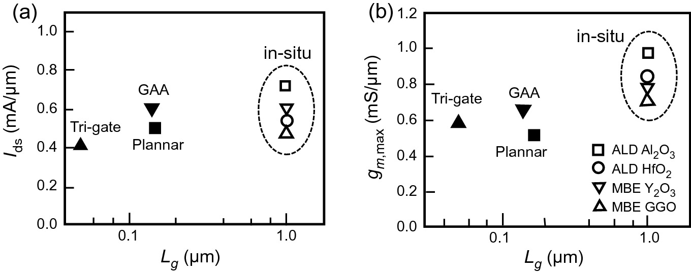
Using in situ deposition, and in situ and ex situ ALD approaches, various high-κ/III–V inversion-mode MOSFETs using GaAs, InGaAs, and GaN as channel materials have been demonstrated. Among them, the In0.53Ga0.47As MOSFET is the most extensive studied due to its high electron mobility, high saturation velocity, and smaller charge neutrality level below the conduction band minimum of the channel material. Figure 9.55 benchmarks performances of state-of-the-art In0.53Ga0.47As enhancement-mode planar and non-planar MOSFETs incorporated with various high-κ dielectrics. The non-planar structures include tri-gate, multigate, and gate-all-around (GAA) devices. The UHV deposited GGO and Y2O3, in situ ALD HfO2 and Al2O3, and ex situ ALD Al2O3 are used as the gate dielectrics. The drain currents for all devices are compared at the same bias conditions of VDS = 1 V and VGSVT = 1 V. The general trend is that the 1-µm gate length MOSFETs using in situ high-κ dielectrics show better IDS and maximum gm compared to smaller gate length devices with ex situ high-κ dielectrics, even though the bias conditions are not favorable for 1-µm gate length MOSFETs. The 1-µm gate length In0.53Ga0.47As MOSFETs with in situ ALD-Al2O3 dielectrics show superb IDS of 0.72 mA/µm, which compares favorably with other planar and non-planar InGaAs MOSFETs with ex situ ALD-Al2O3 dielectrics and significantly smaller gate lengths. The in situ ALD-Al2O3 MOSFETs also have the best maximum gm of 0.98 mS/µm at VDS = 2 V. Other MOSFETs with UHV deposited GGO and Y2O3, and in situ ALD HfO2 high-κ dielectrics, also show excellent IDS and maximum gm. The low interface trap density associated with in situ high-κ dielectrics is key to the high performances of these devices.
../images/325043_1_En_9_Chapter/325043_1_En_9_Fig55_HTML.png
Fig. 9.55

Benchmark of a drain current at VDS = VGS − VT = 1 V and b peak transconductance of in situ high-κ dielectrics/In0.53Ga0.47As MOSFETs and other enhancement-mode planar and non-planar devices using ex situ (solid symbols) high-κ dielectrics.

Reprinted with permission from [25], copyright AIP Publishing

During the past two decades, tremendous progress has been made in realizing both enhancement-mode and depletion-mode high-κ dielectrics/III–V MOSFETs. However, there exist several difficult challenges to overcome before III–V materials become appropriate for future high-speed, low-power logic applications. First, for III–V MOSFETs to be competitive against scaled Si MOSFETs, their physical gate length needs to be scaled to 30 nm and below with acceptable ION/IOFF ratio (>104) at VCC = 0.5 V. Recent demonstration of high-performance devices described above has already laid a solid foundation in achieving this goal. Second, for CMOS logic applications, there is a need for p-channel MOSFETs with very high hole mobility. Although III–V materials show 10–20 times better electron mobility compared to Si, their hole mobility is comparable to that of Si. To improve the hole mobility in III–V materials, one approach is to use compressively strained III–V channels in MOSFETs. Alternatively, other novel materials exhibiting high hole mobility, e.g., strained Ge quantum wells, can be used as the p-channel materials. Finally, to take advantage of the advanced development of Si IC technologies and the high-speed, low-power capabilities of III–V devices, it is desirable to monolithically integrate III–V devices selectively onto the Si platform. To achieve this goal, one has to solve two significant challenges, namely the lattice-mismatch and thermal mismatch between Si and III–V’s.

Problems
  1. 1.

    Refer to the experimental results of an Al0.3Ga0.7As/GaAs HEMT reported in [6].

    1. (a)

      Estimate the threshold voltage VT for three samples (R-96A, R-73A, and R-72A).

       
    2. (b)

      The 2DEG in the triangular quantum well has a sine-wave-like distribution perpendicular to the conduction channel. What is the average concentration peak of the 2DEG located ΔW away from the heterojunction interface? The results can be calculated using the equation

      $$ N_{S} = \frac{{\epsilon_{2} }}{{q\left( {W_{d} +\Delta W} \right)}}\left( {V_{\text{GS}} - V_{T} - V_{x} } \right) $$

      Assume VDS = 0 and comment on your results in terms of whether they are realistic.

       
    3. (c)

      Estimate ΔW again using Howard–Fang approximation for the triangular QW at the interface. Also discuss your results.


  1. 2.

    In an Al0.2Ga0.8As/Ga0.85In0.15As pseudomorphic high-electron-mobility transistor (pHEMT), the Al0.2Ga0.8As barrier is uniformly doped at a level of 2 × 1018 cm−3. At the Al0.2Ga0.8As/Ga0.85In0.15As interface, there is an undoped spacer layer on the Al0.2Ga0.8As side.

    1. (a)

      Calculate the sheet carrier concentration in the triangular Ga0.85In0.15As quantum well for different spacer layer thickness (Wsp) of 25 Å and 100 Å. Assume the donor level in Al0.2Ga0.8As is sufficiently deep (Ed = 50 meV) so that the Fermi level is pinned there. The dielectric constant of Ga0.85In0.15As is 13.41ε0.

       
    2. (b)

      Plot the equilibrium energy band diagram of the whole pHEMT structure, including metal contact, for the Wsp = 25 Å case using SimWindows. Assume the total Al0.2Ga0.8As barrier has a thickness of 150 Å and the undoped Ga0.85In0.15As 2DEG channel is 100 Å thick. The whole structure is grown on top of an undoped GaAs substrate. The metal-Al0.2Ga0.8As work function m equals ~0.9 eV.

       
    3. (c)

      Repeat part (a) for a modulation-doped Al0.3Ga0.7As/GaAs heterostructure with a 25 Å spacer layer and ΔEc = 0.2 eV. This HEMT structure has the same doping level in the Al0.3Ga0.7As barrier. The dielectric constant of GaAs is 12.85$$ \epsilon_{0} $$.

       
    4. (d)

      Now the 2DEG channel material of the pHEMT is replaced with a GaAs0.8Sb0.2 layer, but keep all other materials unchanged. For Wsp = 25 Å, calculate the sheet carrier concentration in the triangular GaAsSb QW. Will this material system outperform the Al0.2Ga0.8As/Ga0.85In0.15As pHEMT structure? Why?


The relevant material parameters are listed below:

For Ga0.85In0.15As: $$ m_{e}^{*} /m_{0} $$ = 0.025(1 − x) + 0.71x − 0.0163x(1 − x)

For GaAs0.8Sb0.2: $$ m_{e}^{*} /m_{0} $$ = 0.00634 − 0.0483x − 0.0252x2.
  1. 3.

    The 2DEG with a sheet carrier density of 1013 cm−2 is obtained at the interface of an AlxGa1−xN/GaN HEMT structure grown by MOCVD. The AlxGa1−xN barrier is undoped and has a thickness of 30 nm. Using parameters provided in the reference article [9], verify that the Al-composition (x) of the AlxGa1−xN barrier is about 0.2 as shown in Fig. 11 of the referenced article.

     
  2. 4.

    Repeat Problem 3 with up-to-date material parameters of AlxGa1−xN shown below:


ΔEc(x) ≈ 2.12x,

Eg(x) = xEg(AlN) + (1–x)Eg(GaN) − 0.7x(1–x).

Dielectric constant $$ \epsilon $$(x) = 9.5 − x,

m*(x) = 0.22me,

m(x) = 1.3x + 0.84 (eV).

$$ P_{\text{SP}} \left( {{\text{Al}}_{x} {\text{Ga}}_{1 - x} {\text{N}}/{\text{GaN}}} \right) = - 0.090x - 0.034\left( {1 - x} \right) + 0.021x\left( {1 - x} \right)\;{\text{c/m}}^{2} $$
$$ P_{\text{PE}} \left( {{\text{Al}}_{x} {\text{Ga}}_{1 - x} {\text{N}}/{\text{GaN}}} \right) = - 0.0525x + 0.0282x\left( {1 - x} \right)\;{\text{c/m}}^{2} \; \qquad \qquad \qquad  $$
Assuming the Al-composition of the AlxGa1−xN barrier in the AlxGa1−xN/GaN HEMT is x = 0.2, calculate the 2DEG sheet carrier density at the AlxGa1−-xN/GaN interface.
  1. 5.
    The active region of a p-channel pseudomorphic high-hole-mobility transistor (pHHMT) has a compressively strained InSb channel material and an Al0.35In0.65Sb barrier. For a 5 nm InSb QW sandwiched between Al0.35In0.65Sb barrier, the type-I band discontinuities, ΔEc and ΔEv, are determined as 0.342 and 0.254 eV, respectively. Assume the 200 Å thick Al0.35In0.65Sb barrier consists of a uniformly Be-doped layer of p = 1018 cm−3 and an undoped spacer layer, Wsp = 70 Å.
    1. (a)

      Calculate the sheet carrier concentration in the triangular InSb quantum well. Assume the acceptor level in Al0.35In0.65Sb is sufficiently deep (Ea = 40 meV) so that the Fermi level is pinned there.

       
    2. (b)

      Plot the equilibrium energy band diagram of the whole pHHMT structure, including metal contact, using SimWindows. The plot should extend into the AlInSb buffer layer for 200 Å. Assume the metal-Al0.35In0.65Sb work function m equals ~0.16 eV.


  2. 6.

    In pursuing high-speed HBTs, InP-based material systems are the most promising. One of the systems being actively studied is based on using GaSb0.5As0.5 lattice-matched to InP as the base material.

    1. (a)

      Find the band discontinuity values between lattice-matched GaSb0.5As0.5 and InP. Is this a type-I or type-II heterojunction?

       
    2. (b)

      In Ga0.47In0.53As/InP N-p-N DHBTs, the valence band discontinuity between InP emitter and Ga0.47In0.53As base is 0.36 eV. The ΔEc in this type-I heterojunction is 0.252 eV. By replacing the Ga0.47In0.53As with lattice-matched GaSb0.5As0.5, the maximum current gain can be improved. Calculate the maximum current gain improvement.

       
    3. (c)

      Compare the properties of GaSb0.5As0.5/InP and Ga0.47In0.53As/InP HBTs.


  3. 7.

    GaxIn1−xP is a useful material for visible light-emitting and HBT applications.

    1. (a)

      Calculate the composition x and band gap energy of GaxIn1−xP lattice-matched to GaAs.

       
    2. (b)

      Using model-solid theory, calculate the band discontinuities between lattice-matched GaxIn1−xP and GaAs.

       
    3. (c)

      In Al0.3Ga0.7As/GaAs HBTs, the valence band discontinuity between Al0.3Ga0.7As emitter and GaAs base is 0.132 eV. By replacing the Al0.3Ga0.7As with lattice-matched GaxIn1−xP the maximum current gain can be improved. Calculate the magnitude of current gain improvement.

       
    4. (d)

      Does GaxIn1−xP offer any advantages over Al0.3Ga0.7As as the barrier layer in an GaxIn1−xP/GaAs high-electron mobility transistor? Why? Note, the conduction band discontinuity in the Al0.3Ga0.7As/GaAs system is 0.263 eV.


  4. 8.

    Mini project: During the last 60 years, the density and feature size of Si ICs have followed Moore’s law faithfully through device scaling. However, the current Si technology will hit a feature size limit in the near future. New channel materials for increased electron and hole mobility, well above those achievable in strained Si, are needed. As gate dielectric scaling becomes increasingly difficult, carrier transport enhancement will become essential for current enhancement in the advanced FETs of future CMOS generations. One of the major problems encountered in developing FETs based on materials other than Si is the large disparity between electron and hole mobility. In order to design complementary FETs (i.e., one n-channel and one p-channel, and not limited to MOSFET), a material system with high hole mobility is required.


In this problem, the goal is to design a p-channel quantum well FET (QWFET) similar to the high-hole-mobility QWFET reported by Intel in 2008. (M. Radosavljevic et al., 2008 IEEE IEDM Tech. Dig., https://​doi.​org/​10.​1109/​iedm.​2008.​4796798)

Your work should meet the following requirements:
  • Select a material system among all available III–V materials for high hole mobility. Explain why you select it. However, you cannot copy the structure reported by Intel. Recall that in Chap. 6, we learned that under compressive strain, the heavy-hole band is lifted above the light-hole band in the growth direction (perpendicular to surface). But in the direction parallel to the surface (perpendicular to the growth direction), the effective mass becomes lighter. (See S. L. Chuang, Phys. Rev., B43, 9649, 1991.)

  • The selected material system should be able to form QWFET structures with high crystal quality. Of course, high-quality heterostructures prepared on metamorphic substrate structures are allowed. (That means you can use materials with any lattice constant as the substrate).

  • Design the layer structure of a QWFET based on the material system selected. We restrict the selection of FET structure to QWFETs (including pseudomorphic structures). Provide detailed material and device parameters such as ΔEv, NS and layer structures along with full energy band diagram. For heterostructures, the energy band discontinuities should be calculated. The portion of gate contact should also be included.

  • To simplify the calculation, set the spacer layer thickness as Wsp = 25 Å and the acceptor level in the barrier layer as Ea = 40 meV. The Schottky barrier height of the barrier layer can be determined following the method reported by Tiwari and Frank (Appl. Phys. Lett., 60, 630, 1992).

  • Your final device layer structure should be a depletion mode FET at zero gate bias.