Chapter 4. Chips, Ahoy!
Before I get into the fascinating topic of integrated circuit chips (often referred to as ICs or simply chips), I have to make a confession. Some of the things I asked you to do in previous experiments could have been done a bit more simply, if we had used chips.
Does this mean you have been wasting your time? Absolutely not! I firmly believe that by building circuits with individual components such as transistors and diodes, you acquire the best possible understanding of the principles of electronics. Still, you are going to find that chips containing dozens, hundreds, or thousands of transistor junctions will enable some shortcuts.
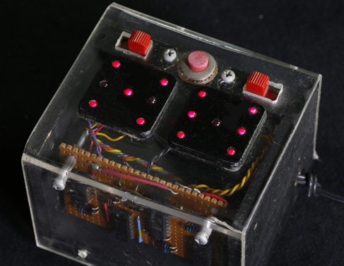
You may also find chips curiously addictive to play with—although you may not become quite as excited as the character in Figure 4-1.
The tools, equipment, components, and supplies described below will be useful in Experiments 16 through 24, in addition to items that have been recommended previously.

Figure 4-1. My role model.
Necessary Items for Chapter Four
The only new tool that you might consider using in conjunction with chips is a logic probe. This tells you whether a single pin on a chip has a high or low voltage, which can be helpful in figuring out what your circuit is doing. The probe has a memory function so that it will light its LED, and keep it lit, in response to a pulse that may have been too quick for the eye to see.
Some of my readers disagree with me, but I regard the logic probe as optional, not essential. Search online and buy the cheapest one you can find. I don’t have any specific brand recommendations.
Components
As before, if you want kits containing components, see “Kits”. If you prefer to buy your own components from online sources, see “Components”. For supplies, see “Supplies”.
Fundamentals: Choosing Chips
Figure 4-2 shows two integrated circuit chips. The one at the top is of the old-school, through-hole design, with pins spaced at 1/10” so that they will fit through the holes in your breadboard or perforated board. These are the chips I will be using exclusively, because they’re easy to handle. The smaller chip is a surface-mount design, which I will not be using, because they don’t fit breadboards or perforated boards and are difficult to handle.
Many through-hole and surface-mount chips are functionally identical. The only difference is the size (although some surface-mount versions use a lower voltage).
The body of a chip is usually made of plastic or resin and is often referred to as the package. The traditional chip is usually sold in a dual-inline package, meaning that it has two (i.e., dual) rows of pins. The acronym for this package is DIP or (when it is made of plastic) PDIP.
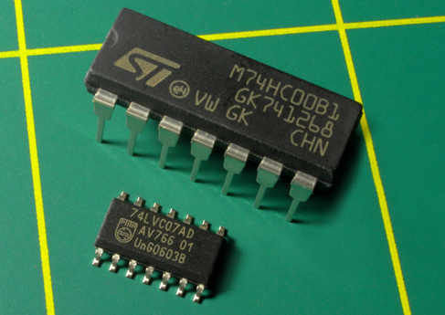
Figure 4-2. A through-hole chip (top) and surface-mount chip (bottom).
Surface-mount packages often are identified with acronyms beginning with letter S, as in SOIC, meaning small-outline integrated circuit. Numerous surface-mount variants exist, with different pin spacing and other specifications. They are all outside the scope of this book, and if you buy your own components, you should be careful not to select them by mistake.
Inside the package, the circuit is etched on a tiny wafer of silicon, which is where the term “chip” comes from, although the whole component is now usually referred to as a chip, and I will follow that convention here. Tiny wires inside the package link the circuit with the rows of pins that protrude on either side.
The PDIP chip in Figure 4-2 has seven pins in each row, making a total of 14. Other chips may have 4, 6, 8, 16, or more pins.
Just about every chip has a part number printed on it. Notice in the photograph that even though the chips look quite different from each other, they both have “74” in their part numbers. This is because both of them are members of the family of logic chips that were assigned part numbers from 7400 and upward when they were introduced several decades ago. This is often referred to as the 74xx family, and I’ll be using these chips a lot.
Take a look at Figure 4-3. The initial letters identify the manufacturer, which you can ignore, as it really makes no difference for our purposes. (If you are wondering why “SN” identifies Texas Instruments, it’s because the company used to call their chips “semiconductor networks” in the early days.)
Skip the letters until you get to the “74.” After that, you find two more letters, which are important. The 7400 family has evolved through many generations, and the letter(s) inserted after the “74” tell you which generation you’re dealing with. Generations have included: 74L, 74LS, 74C, 74HC, and 74AHC. There are many more.

Figure 4-3. How to decode the part number of a chip in the 74xx family.
Generally speaking, later generations tend to be faster or more versatile than earlier generations. In this book, I am using the HC generation of the 7400 family exclusively, because almost all 7400 chips are available in it, the cost is moderate, and the chips don’t use a lot of power. For our purposes, the extra speed offered by later generations is not relevant—although you can certainly use the HCT generation if you prefer.
Following the letters identifying the generation, you’ll find a sequence of two, three, four, or (sometimes) five digits. These identify the specific function of the chip. Following the digits is another letter, or two letters, or more. For our purposes, those terminating letters are not important.
Looking back at Figure 4-2, the DIP chip part number, M74HC00B1, tells you that it is a chip made by STMicroelectronics, in the 74xx family, HC generation, with its function identified by numerals 00.
The purpose of this long explanation is to enable you to interpret catalog listings if you go chip shopping. You can search for “74HC00” and the search engines at online vendors are usually smart enough to show you appropriate chips from multiple manufacturers, even though there are letters preceding and following the term that you’re searched for.
Just be sure that they will fit your breadboard. Limit your search results to DIP, PDIP, or through-hole packages. If the part number begins with SS, SO, or TSS, it’s absolutely definitely surface-mount, and you don’t want it. For a lot more information on searching and shopping, see “Searching and Shopping Online”.
All the chips needed for the experiments in this chapter of the book are listed in Figure 6-7. You will need a few other types of components, which I will list here.
Optional: IC Sockets
If you plan to immortalize any of your circuits in solder, I suggest you avoid soldering chips directly, because if you make a wiring error or damage the chip, you have to desolder multiple pins in order to remove it. This is very difficult. To avoid the problem, buy some DIP sockets, solder the sockets onto the board, and then plug the chips into the sockets. You can use the cheapest sockets you can find (you don’t need gold-plated contacts for our purposes). You will need 8-pin, 14-pin, and 16-pin sockets. Quantity of each: 5 minimum. Two sockets are shown in Figure 4-4.
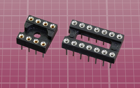
Figure 4-4. To avoid the risk of damaging a chip by soldering it directly, it can be mounted in an IC socket after the socket has been soldered into a circuit board.
Essential: Subminiature Slide Switch
A slide switch has a tiny lever that you slide to and fro with the tip of your finger, making and breaking an electrical contact inside the switch, as shown in Figure 4-5. It has three pins spaced 0.1” apart (2.54mm in metric). If you buy your own components, see “Other Components” and go down to the subhead “Components for Chapter Four” for more information about switches.
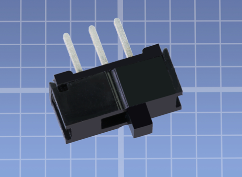
Figure 4-5. The subminiature slide switch recommended for projects in this book.
Caution: Switching Overload
A very small slide switch is not designed to switch significant currents or voltages. It is designed for low-powered circuits. A limit may be as low as 100mA at 12VDC. This is sufficient for our purposes. Check the manufacturer’s datasheet if you want a slide switch to do more than this.
Essential: Low-Current LEDs
HC series logic chips are not designed to deliver current much beyond 5mA. You can take as much as 20mA from them to drive an LED, but this will pull down the output voltage, making it unsuitable as an input to other logic chips. I am suggesting low-current LEDs for all your experiments with logic chips.
Remember that low-current LEDs require higher-value series resistors, because they don’t tolerate as much current as generic LEDs. I will mention this wherever it is important.
Essential: Numeric Displays
One of the chip projects will display its output using seven-segment numeric displays—the simple kind of digits that you still find on digital clocks and microwave ovens. See Figure 4-6. For purchasing information, see “Other Components” and go down to the subhead “Components for Chapter Four.”
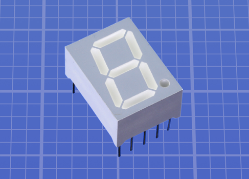
Figure 4-6. Seven-segment displays are the cheapest way to show a numeric output and can be driven directly by some CMOS chips.
Essential: Voltage Regulator
Because many logic chips require precisely 5 volts DC, you need a voltage regulator to guarantee this. The LM7805 does the job. The chip number will be preceded or followed with an abbreviation identifying the manufacturer and package style, as in the LM7805CT from Fairchild. Any manufacturer will do, but the regulator should look like the one in Figure 4-7. (This is known as the TO220 package style.) You need them in any logic circuit, so five would be a good number to have available.
Optional Extras
To complete the alarm system in Experiment 18, you will require magnetic sensors that you can apply to doors or windows, such as the Directed model 8601, available from dozens of sources online.
If you expect to move a project from a breadboard to a permanent enclosure, the tactile switches that you have been using will be insufficiently sturdy or accessible. For Experiment 18, you will need a full-size DPDT pushbutton switch, ON-(ON) type, with solder terminals. If you search eBay for “DPDT pushbutton” there will be no shortage of options.
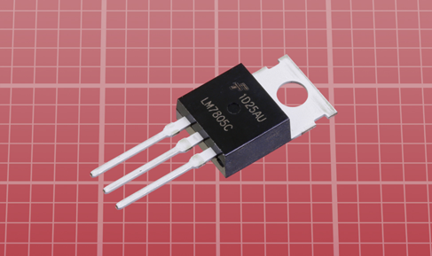
Figure 4-7. Many integrated circuit chips require a controlled power supply of 5 volts, which can be delivered by this regulator from a supply of 7.5 to 12 volts.
Background: How Chips Came to Be
The concept of integrating solid-state components into one little package originated with British radar scientist Geoffrey W. A. Dummer, who talked about it for years before he attempted, unsuccessfully, to build one in 1956. The first true integrated circuit wasn’t fabricated until 1958 by Jack Kilby, working at Texas Instruments. Kilby’s version used germanium, as this element was already in use as a semiconductor. (You’ll encounter a germanium diode when I deal with crystal radios in Experiment 31.) But Robert Noyce, pictured in Figure 4-8, had a better idea.

Figure 4-8. Robert Noyce, who patented the integrated circuit chip and cofounded Intel.
Born in 1927 in Iowa, Noyce moved to California in the 1950s, where he found a job working for William Shockley. This was shortly after Shockley had set up a business based around the transistor, which he had coinvented at Bell Labs.
Noyce was one of eight employees who became frustrated with Shockley’s management and left to establish Fairchild Semiconductor. While he was the general manager of Fairchild, Noyce invented a silicon-based integrated circuit that avoided the manufacturing problems associated with germanium. He is generally credited as the man who made integrated circuits possible.
Early applications were for military use, as Minuteman missiles required small, light components in their guidance systems. These applications consumed almost all chips produced from 1960 through 1963, during which time the unit price fell from around $1,000 to $25 each, in 1963 dollars.
In the late 1960s, MSI (medium-scale integration) chips emerged, each containing hundreds of transistors. LSI (large-scale integration) enabled tens of thousands of transistors on one chip by the mid-1970s, and today’s computer chips can contain several billion transistors.
Robert Noyce eventually cofounded Intel with Gordon Moore, but died unexpectedly of a heart attack in 1990. You can learn more about the fascinating early history of chip design and fabrication at the Silicon Valley Historical Association.
Experiment 16: Emitting a Pulse
I’m going to begin our experiments with chips by introducting you to the most successful one ever made: the 555 timer. You can find numerous guides to it online, so why do I need to discuss it here? I have three reasons for doing so:
It’s unavoidable. You simply have to know about this chip. Some sources estimate that more than 1 billion are still being manufactured annually. It will be used in one way or another in most of the remaining circuits in this book.
It’s useful. The 555 is probably the most versatile chip that exists, with endless applications. Its relatively powerful output (rated at up to 200mA) is extremely useful, and the chip itself is hard to damage.
It’s misunderstood. After reading literally dozens of guides, beginning with an early Signetics datasheet and making my way through various hobby texts, I concluded that the inner workings of the chip are seldom explained on an introductory level. I want to give you a graphic understanding of what’s happening inside it, because if you don’t have this, you won’t be in a good position to use the chip creatively.
What You Will Need
-
Breadboard, hookup wire, wire cutters, wire strippers, multimeter
-
9VDC power supply (battery or AC adapter)
-
Resistors: 470 ohms (1), 10K (3)
-
Capacitors: 0.01µF (1), 15µF (1)
-
Trimmer potentiometers: 20K or 25K (1), 500K (1)
-
555 timer chip (1)
-
Tactile switches (2)
-
Generic LED (1)
Know Your Chips
The pins of a 555 timer are numbered counterclockwise (seen from above), as shown in Figure 4-9. The package has a notch, or a dimple, or both, at the end which is considered the top. The pin spacing is 1/10”.
All other through-hole chips have the same specification, although they may have more pins. Usually (not always) the horizontal spacing between the two rows of pins is 3/10”, which means that the chip neatly straddles the channel down the middle of a breadboard, and the conductors inside the breadboard allow you to have access to each pin of the chip. Yes, that’s why the breadboard is designed that way.
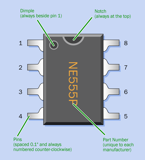
Figure 4-9. The package design of an eight-pin chip. While virtually all chips have a semicircular notch at the top, some do not have a dimple beside pin 1.
Monostable Test
The pins on a 555 timer also have names, as shown in Figure 4-10. A diagram like this tells you the pinouts of the chip. I’ll be explaining the function of each pin—but as usual, I prefer you to make a preliminary investigation of your own.
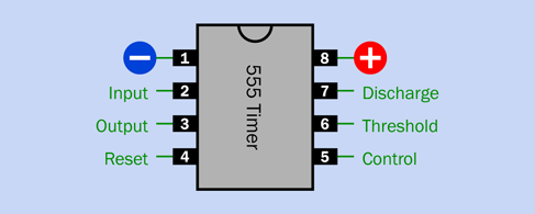
Figure 4-10. The pinouts of the 555 timer chip.
The schematic of a test circuit for the timer is shown in Figure 4-11.

Figure 4-11. A circuit to assist in your investigation of the 555 timer chip.
You can set up this circuit on a breadboard as shown in Figure 4-12. Note that near the bottom-left corner there is a short red jumper connecting the top section of the positive bus to the section immediately below it. The jumper is there in case your breadboard is the type that has a break in its bus.
The component values are shown in Figure 4-13. To assist you in visualizing the connections, an x-ray version is shown in Figure 4-14.
Apply some power, and nothing happens. The timer is waiting for you to trigger it. Set it up by turning the 500K trimmer to the middle of its range.
Now rotate the 20K trimmer all the way counterclockwise, and press button A. If still nothing happens, rotate the 20K trimmer all the way clockwise, and try again. One of these settings or the other should create a pulse from the LED, depending on which way around you plugged in your trimmer. If you don’t get anything, there is an error in your circuit.
Check the schematic, and you see that pin 2 of the timer—the trigger pin—is hardwired through a 10K resistor to the positive side of the power supply. But a purple wire also connects with the trigger pin, and runs down, through a tactile switch, to the trimmer. If the trimmer is rotated so that the wiper connects directly to the negative ground side of the power supply, this will allow the tactile switch to overwhelm the 10K resistor and apply low voltage to pin 2. This triggers the timer.
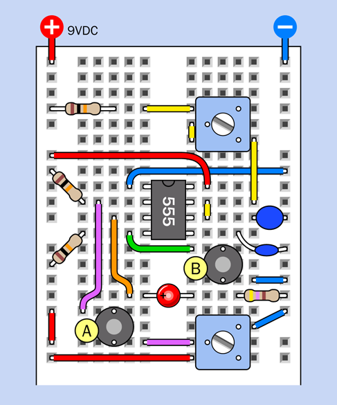
Figure 4-12. Breadboarded version of the timer test circuit.
If the 20K trimmer is turned all the way in the opposite direction, button A will apply positive voltage directly to pin 2, and because pin 2 already has positive voltage through the 10K resistor, an additional positive voltage through button A makes no difference.
-
Positive voltage on the trigger pin is ignored by the chip.
-
A drop in voltage on the trigger pin will trigger the chip.
But, how positive is positive, and how much of a drop will be low enough to act as a trigger? Let’s find out.
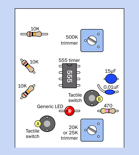
Figure 4-13. Component values for the timer test circuit.
Get out your meter, set it to measure DC volts, and measure the voltage between pin 2 and negative ground while you adjust the 20K trimmer to various settings and press button A. I’m betting that when you press the button to apply a voltage below 3 volts to pin 2, the timer will flash the LED. Above 3 volts, I doubt that anything will happen.
-
The timer is triggered by a voltage on its trigger pin that is one-third of the supply voltage (or less).
-
The LED will continue to glow after you release the button.
-
You can press the button for any length of time that is less than the timer’s cycle time, and the LED always emits the same length of pulse.
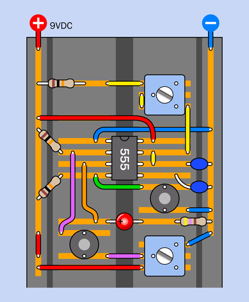
Figure 4-14. Connections inside the breadboard wired for the timer test.
Figure 4-15 shows how the timer is behaving, in graphical format. The 555 converts the imperfect world around it into a precise and dependable output. It doesn’t switch on and off absolutely instantly, but is fast enough to appear instant.
Now try triggering the timer while you turn the 500K trimmer to different positions. You will find that this adjusts the length of the pulse.
-
The resistance between pin 7 and the positive side of the power supply determines how long the pulse from the timer will last (in conjunction with the capacitor on pin 6).
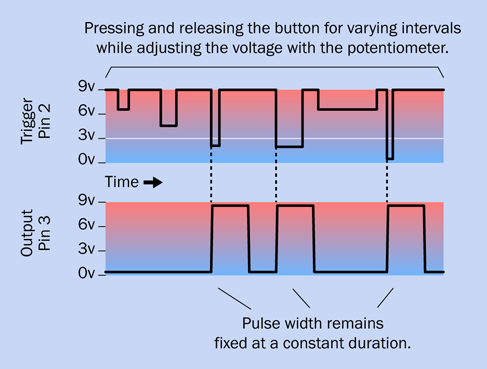
Figure 4-15. How a 555 timer responds to different durations and voltages on its trigger pin.
Here’s another thing to try. Set the 500K trimmer to give a long pulse. Press button A, and then quickly press button B, which will stop the pulse before it completes. Hold down button B while you try to trigger the timer again with button A, and nothing happens.
-
Pin 4 is the reset pin. When you ground it, you force the timer to interrupt whatever it is doing, and it is immobilized until you release pin 4 from its connection with negative ground.
Lastly, let go of button B, hold down button A, and continue to hold it down. This prolongs the pulse from the timer, until you let go of button A.
Regarding the 10K resistors attached to pins 2 and 4—these are known as pullup resistors, because they hold the pins at a positive level. A more direct connection to negative ground will overwhelm the pullup resistor.
The concept of a pullup resistor is important when you are dealing with chips, because you must never allow an input pin to remain unconnected. An unconnected pin is said to be floating, and can cause trouble, as it may pick up stray electromagnetic fields, and we won’t know what voltage is on it from one moment to the next.
Is there such a thing as a pulldown resistor? Absolutely. But the 555 timer needs pullup resistors, because pin 2 or pin 4 is kept in a normal state by positive voltage, and is activated by a low voltage.
-
The 555 timer is triggered or reset by negative voltages on pins 2 and 4 respectively.
Timing the Pulse
If you study the schematic in Figure 4-11, you can see that positive current reaches pin 7 (the discharge pin) by passing through a 10K resistor and a 500K trimmer. (The 10K resistor is there because pin 7 should not be connected directly to the positive side of the power supply.)
You can also see that after passing through the 500K trimmer, the current can reach a 15µF capacitor. Hmmmm, a resistor followed by a capacitor—does this look like an RC network? Is the timer using the combination of the resistance and the 15µF capacitor to determine the length of the output pulse?
Yes, that’s exactly what is going on. Inside the timer chip, some clever electronics are sensing the voltage on the 15µF capacitor, and the timer uses this to terminate its output pulse.
You can measure this yourself. Set the 500K trimmer to create a long pulse, and use your meter to measure the voltage on the left side of the 15µF capacitor. You should see it climbing up—until it reaches about 6 volts. The timer uses this as a signal to stop its output pulse, and the voltage quickly goes down again, because the timer is grounding it internally. This is why pin 7 is known as the discharge pin: the timer discharges the capacitor through it.
-
When the voltage on the timing capacitor reaches two-thirds of the supply voltage, the timer ends its output pulse.
But why are the discharge pin and the threshold pin tied together? You’ll learn about that in the next experiment, when the timer is rewired to deliver a series of pulses, instead of just one. At that time, the timer will be running in astable mode. Currently, you are using it in monostable mode.
-
In monostable mode, the timer delivers only one pulse in response to a triggering event.
-
In astable mode, the timer delivers a continuing series of pulses.
Finally, you may be wondering about the purpose of the 0.01µF capacitor attached to pin 5. This pin is the “control” pin, which means that if you apply a voltage to it, you can control the sensitivity of the timer. Because we are not using this function yet, it’s good practice to put a capacitor on pin 5 to protect it from voltage fluctuations and prevent it from interfering with normal functioning.
Caution: Beware of Pin-Shuffling!
In all of the schematics in this book, chips are shown exactly as you would see them on a breadboard, with the pins in numerical sequence.
Other schematics that you may find, on websites or in books, do things differently. For convenience in drawing circuits, people often resequence the pin numbers. Also, there is no attempt to replicate a breadboard layout with a positive bus and a negative bus at each side. To give you an example, in Figure 4-16 the circuit is identical to that in Figure 4-11, but the pins have been shuffled to simplify connections and minimize wiring crossovers.
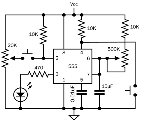
Figure 4-16. This circuit is identical in function to the test circuit shown previously, but pins on the chip have been resequenced to simplify the schematic.
Pin shuffling can create a circuit that is easier to understand in some ways (especially if positive power is at the top and ground at the bottom), but you have to convert the layout, often using pen and paper, before you can build it on a breadboard.
Fundamentals: Timer Duration
When you made your own RC network in Experiment 9, some annoying calculations were necessary to figure out how long a capacitor would take to reach any particular voltage. Using a 555 timer, everything is much easier. You just look up the duration of its output pulse in a table such as the one in Figure 4-17. The resistance between pin 7 and the positive side of the power supply is shown along the top of the table, the value of the timing capacitor is shown down the left side, and the numbers in the table tell you the approximate pulse duration in seconds.
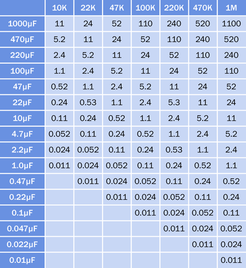
Figure 4-17. Pulse duration, in seconds, of a 555 timer running in monostable mode, for values of the timing resistor and timing capacitor. Times are rounded to two digits.
-
Resistor values below 1K should not be used.
-
Resistor values below 10K are undesirable, as they increase power consumption.
-
Capacitor values above 100µF may produce inaccurate results because leakage in the capacitor becomes comparable with its charging rate.
What if you want a time longer than 1,100 seconds or shorter then 0.01 seconds? Or what if you want a pulse duration that falls somewhere between the values in the table?
You can use this simple formula, where T is the pulse time in seconds, R is the resistance in kilohms, and C is the capacitance is microfarads.
T = R × C × 0.0011
Bear in mind that the result may not be exact, because resistor and capacitor values can be inaccurate, and because of other factors such as ambient temperature.
Theory: Inside the 555 in Monostable Mode
The plastic body of the 555 timer contains a wafer of silicon on which are etched dozens of transistor junctions in a pattern that is too complex to be explained here. However, I can summarize their function by dividing them into groups, as shown in Figure 4-18.
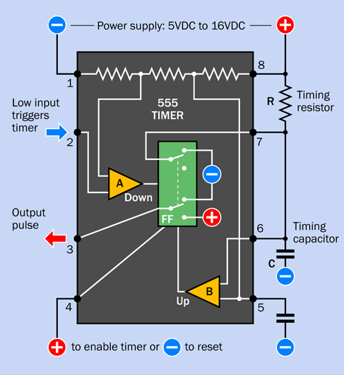
Figure 4-18. Simplified representation of internal functions of a 555 timer, wired in monostable mode.
The negative and positive symbols inside the chip are power sources that actually come from pins 1 and 8, respectively. I omitted the internal connections to those pins for the sake of clarity.
The two yellow triangles are comparators. Each comparator compares two inputs (at the base of the triangle) and delivers an output (from the apex of the triangle) depending on whether the inputs are similar or different. FF is a flip-flop, a logic component that can rest in one state or the other. I have depicted it as a double-throw switch, although in reality it is solid-state.
Initially when you power up the chip, the flip-flop is in its “up” position, which delivers low voltage through the output, pin 3. If the flip-flop receives a signal from comparator A, it flips to its “down” state, and flops there. When it receives a signal from comparator B, it flips back to its “up” state, and flops there. The “Up” and “Down” labels on the comparators will remind you how each one changes the switch when it is activated. Some people feel that the term “flip-flop” is derived from it having two states named “flip” and “flop.” But I prefer to think of it flipping and flopping.
Notice the external wire that connects pin 7 with capacitor C. As long as the flip-flop is “up,” it sinks the positive voltage coming through resistor R to pin 7, and prevents the capacitor from charging positively.
If the voltage on pin 2 drops to 1/3 of the supply, comparator A notices this, and flips the flip-flop to its “down” position. This sends a positive pulse from pin 3, the output pin, and also disconnects the negative power from pin 7. Now the capacitor can start charging through the resistor. While this is happening, the positive output from the timer continues.
As the voltage increases on the capacitor, comparator B monitors it through pin 6. When the capacitor accumulates 2/3 of the supply voltage, comparator B sends a pulse to the flip-flop, flipping it back into its original “up” state. This discharges the capacitor through pin 7. Also, the flip-flop ends the positive output through pin 3 and replaces it with a negative voltage. This way, the 555 returns to its original state.
I’ll sum up this sequence of events:
-
Initially, the flip-flop grounds the capacitor and grounds the output (pin 3).
-
A drop in voltage on pin 2 to 1/3 of the supply voltage or less makes the output (pin 3) positive and allows capacitor C to start charging through resistor R.
-
When the capacitor reaches 2/3 of the supply voltage, the chip discharges the capacitor, and the output at pin 3 goes low again.
Fundamentals: Pulse Suppression
When power is first applied to a timer that is configured in monostable mode, the timer tends to emit one pulse spontaneously before going dormant and waiting to be triggered again. This can be annoying in many circuits.
One way to prevent it is by putting a 1µF capacitor between the Reset pin and negative ground. The capacitor sinks current from the Reset pin when the power is first turned on, and holds the pin low for a fraction of a second—just long enough to stop the timer from emitting its waking-up pulse. After the capacitor is charged, it doesn’t do anything more, and a 10K resistor holds the reset pin positive, so it won’t interfere with the running of the timer.
I’ll be using the pulse-suppression concept in subsequent experiments.
Fundamentals: Why the 555 Is Useful
In its monostable mode, the 555 will emit a single pulse of fixed (but programmable) length. Can you imagine some applications? Think in terms of the pulse from the 555 controlling some other component. A motion sensor on an outdoor light, perhaps. When an infrared detector “sees” something moving, the light comes on, but only for a specific period—which can be controlled by a 555.
Another application could be a toaster. When someone lowers a slice of bread, a switch will close, triggering the toasting cycle. To change the length of the cycle, you could use a potentiometer and attach it to the external lever that determines how dark you want your toast. At the end of the toasting cycle, the output from the 555 would pass through a power transistor, to activate a solenoid (which is like a relay, except that it has no switch contacts) to release the toast.
Intermittent windshield wipers could be controlled by a 555 timer—and on earlier models of cars, they were. The repeat rate of keys on a rather basic computer keyboard could be controlled by a 555 timer—and on the Apple II, it was.
What about the intrusion alarm in Experiment 15? One of the features on my wish list was that it should wait long enough for you to shut it off, before it starts to make a noise. The output from a 555 timer can take care of that.
The experiment that you just performed seemed trivial, but it implies a huge range of possibilities.
Fundamentals: Bistable Mode
There’s another way to use the timer, known as bistable mode. This entails disabling its fundamental features. Why would you want to do this? I will explain.
Figure 4-19 shows a circuit that you can build in just a few minutes. Give it a try. The two resistors on the left are pullup resistors, 10K each. The resistor at the bottom is 470 ohms, to protect the LED. Add two tactile switches, and the timer chip itself, and you’re done.
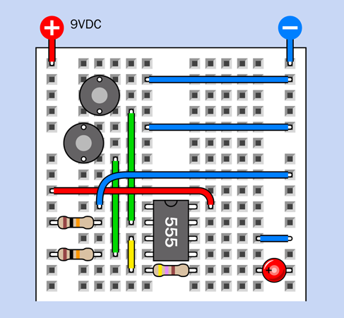
Figure 4-19. Breadboard circuit to make the 555 timer function as a flip-flop.
Once you have it on your breadboard, press and release the top button, and the LED lights up. For how long? For as long as you supply power to the circuit. The output from the timer continues indefinitely.
Now press and release the bottom button, and the LED goes off. For how long? For as long as you like. It won’t come back on until you press the top button again.
I mentioned that there is a flip-flop inside the timer. This circuit makes the timer into one big flip-flop. It flips into its “on” state when you ground pin 2—and it flops there. It flips into its “off” state when you ground pin 4—and it flops there. Flip-flops are very important in digital circuits, as I will explain a bit later, but right now, how does this work, and why would you need it?
Take a look at the schematic in Figure 4-20. You may notice that there is no resistor or capacitor on the righthand side. The RC network is missing. So—this timer circuit has no timing components! Normally, when you trigger the timer, its output pulse ends when the timing capacitor on pin 6 accumulates 2/3 of supply voltage. But pin 6 is grounded, so it can never reach the 2/3 value. Consequently, when you trigger the timer, the output pulse will never end.
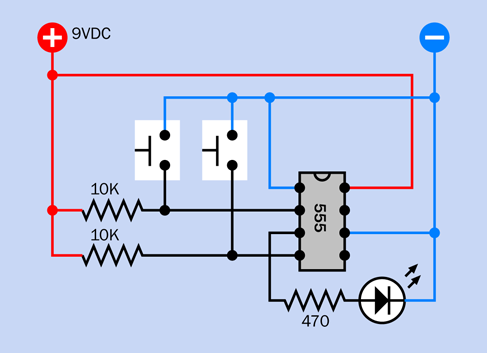
Figure 4-20. A test circuit for the 555 timer in bistable mode.
Of course, you can stop the output by applying a low voltage to the reset pin. But once the output stops, it will remain stopped, so long as you don’t trigger the timer again.
This configuration is called bistable because it is stable when the output is high, and it is stable when the output is low. A simple flip-flop like this can also be called a latch.
-
A negative pulse to pin 2 turns the output positive, and latches it.
-
A negative pulse to pin 4 turns the output negative, and latches it.
You do have to keep pins 2 and 4 high when you are not triggering them. That’s what the pullup resistors in the schematic are for.
It’s OK to leave pin 5 of the timer unconnected, because we’re pushing it into extreme states where any random signals from those pins will be ignored.
As for why you would need to use a timer in this way—you’ll be surprised how useful it can be. I’m going to use it in three experiments in the remainder of this book. The 555 was not really designed to function in bistable mode, but it can be convenient.
Background: How the Timer Was Born
Back in 1970, when barely a half-dozen corporate seedlings had taken root in the fertile ground of Silicon Valley, a company named Signetics bought an idea from an engineer named Hans Camenzind (pictured in Figure 4-21). It wasn’t a huge breakthrough concept—just 23 transistors and a bunch of resistors that would function as a programmable timer. The circuit would be versatile, stable, and simple, but these virtues paled in comparison with its primary selling point. Using the emerging technology of integrated circuits, Signetics could reproduce the whole thing on a silicon chip.

Figure 4-21. Hans Camenzind, inventor, designer, and developer of the 555 timer chip for Signetics.
This entailed some trial and error. Camenzind worked alone, building the whole thing initially on a large scale, using off-the-shelf transistors, resistors, and diodes on a breadboard. It worked, so then he started substituting slightly different values for the various components to see whether the circuit would tolerate variations during production, and other factors such as changes in temperature when the chip was in use. He made at least 10 different versions of the circuit. This took months.
Next came the crafts work. Camenzind sat at a drafting table and used a specially mounted X-Acto knife to scribe his circuit into a large sheet of plastic. Signetics then reduced this image photographically by a ratio of about 300:1. They etched it into tiny wafers, and embedded each of them in a half-inch rectangle of black plastic with the product number printed on top. Thus, the 555 timer was born.
It turned out to be the most successful chip in history, both in the number of units sold (tens of billions and counting) and the longevity of its design (not significantly changed in almost 40 years). The 555 has been used in everything from toys to spacecraft. It can make lights flash, activate alarm systems, put spaces between beeps, and create the beeps themselves.
Today, chips are designed by large teams and tested by simulating their behavior using computer software. Thus, the chips inside a computer enable the design of new chips. The heyday of solo designers such as Hans Camenzind is long gone, but his genius lives inside every 555 timer that emerges from a fabrication facility. If you’d like to know more about chip history, visit the Transistor Museum.
A personal note: in 2010, when I was writing Make: Electronics, I looked up Hans Camenzind online and found that he maintained his own website, which included a phone number. On impulse, I called him. This was a strange moment, to be talking to the man whose chip design I had used for more than 30 years. He was friendly (although he didn’t waste words), and readily agreed to review the text of my book. Even more kindly, after he read it, he gave it a strong endorsement.
Subsequently I bought his own short history of electronics, Much Ado About Almost Nothing, which is still available online, and which I highly recommend. I felt honored to have had the opportunity to talk to one of the pioneers in integrated circuit design. I was sad when I heard of his death in 2012.
Fundamentals: 555 Timer Specifications
-
The 555 can run from a reasonably stable voltage source ranging from 5VDC to 16VDC. The absolute maximum is 18VDC. Many datasheet specifications are measured at 15VDC. The voltage does not have to be controlled by a voltage regulator.
-
Most manufacturers recommend a range from 1K to 1M for the resistor attached to pin 7, but values below 10K draw a more significant amount of current. It’s a better idea to reduce the value of the capacitor than to reduce the value of the resistor.
-
The capacitor value can go as high as you like, if you want to time really long intervals, but the accuracy of the timer will diminish because leakage in the capacitor becomes comparable with its charge rate.
-
The timer imposes a voltage drop that is greater than the drop created by a transistor or a diode. The difference between supply voltage and output voltage will be 1V or more.
-
The output is rated to source or sink 200mA, but an output current above 100mA will pull down the voltage and can affect the timing accuracy.
Caution: Not All Timers Are Equal
Everything I have said so far applies to the old original “TTL” version of the 555 timer. TTL is an acronym for transistor–transistor logic, which preceded modern CMOS chips that use much less power. The TTL version of the timer is also referred to as the bipolar version, as it contains bipolar transistors.
The advantage of the original 555 is that it is cheap and robust. You can’t damage it easily, and its output is powerful enough to connect directly with a relay coil or a small loudspeaker. However, the 555 is not efficient, and tends to generate voltage spikes that sometimes interfere with the operation of other chips.
To address these disadvantages, a newer version of the 555 timer was developed using CMOS transistors, which draw less power. This chip also doesn’t create voltage spikes. But its output is more limited. How much more? That depends on the particular manufacturer.
Unfortunately, there is a lack of standardization among CMOS versions of the 555 timer. Some claim to deliver 100mA while others are limited to 10mA.
Confusingly, the CMOS versions have a variety of part numbers. The 7555 is clearly identified as a CMOS chip, but others merely precede the 555 number with a different group of letters, and it’s up to you to notice, and to understand what they mean.
In this book, to avoid confusion and keep things simple, I am only using the TTL version of the 555 timer, also known as the bipolar version. If you are buying your own, see “Other Components” and go down to the subhead “Components for Chapter Four” where you will find timer buying advice.
Experiment 17: Set Your Tone
Now that you’re familiar with the 555 timer in monostable mode and bistable mode, I want you to get acquainted with it in astable mode—so called because the output fluctuates constantly between high and low, and does not remain stable in either of those states.
This resembles the output of the transistor oscillator that you built in Experiment 11, except that it is much more versatile and easier to control, and instead of requiring two transistors, four resistors, and two capacitors to create the oscillation, you only need one chip, two resistors, and one capacitor.
What You Will Need
-
Breadboard, hookup wire, wire cutters, wire strippers, multimeter
-
9-volt power supply (battery or AC adapter)
-
555 timer chips (4)
-
Miniature loudspeaker (1)
-
Resistors: 47 ohms (1), 470 ohms (4), 1K (2), 10K (12), 100K (1)
-
Capacitors: 0.01µF (8), 0.022µF (1), 0.1µF (1), 1µF (3), 3.3µF (1), 10µF (4), 100µF (2)
-
1N4148 diode (1)
-
Trimmer potentiometer, 100K (1)
-
Tactile switch (1)
-
Generic LEDs (4)
Astable Test
A generic astable circuit is shown in Figure 4-22. I’ve put a loudspeaker on the output, because the timer will be running at an audio frequency. The loudspeaker is driven through a resistor, to limit the current, and a coupling capacitor, which passes audio frequencies while blocking DC. You’ll see the values for these components in the next schematic. Right now I just want you to see the general layout.
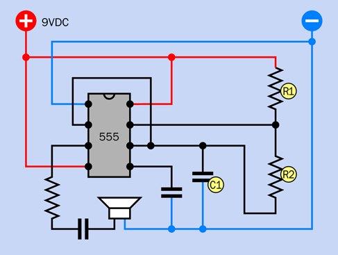
Figure 4-22. A basic, generic circuit that runs a 555 timer in astable mode.
The components labeled R1, R2, and C1 control the speed of the timer. These labels are always used in manufacturers’ datasheets and other sources, so I’m following the same convention.
C1 does the same thing as the timing capacitor in the monostable circuit in Figure 4-11. The need for two resistors, instead of one, will be explained below.
See if you can get a sense of how this circuit may work, using the knowledge that you gained in Experiment 16. The first thing you may notice is that there’s no input. Pin 2 (the trigger pin) is connected back to pin 6 (the threshold pin). Can you see how that’s going to work? C1 will accumulate a charge, as it did when the timer was in monostable mode, until it reaches 2/3 of the power supply, at which point it will discharge through R2 into pin 7, and its voltage will drop. Its connection with pin 2 will mean that the trigger pin senses the drop in voltage on C1. And what does the trigger pin do when the voltage on it drops suddenly? It triggers the timer. So, in this configuration, the timer will retrigger itself.
How fast will that happen? I think you should build a test version of the circuit to find out. In Figure 4-23 I have suggested values for the components and have redrawn the schematic to include a trimmer potentiometer, so that you’ll see (or, rather, hear) the effect of varying this resistance. The trimmer, plus the 10K resistor that precedes it, add up to R2. The timing capacitor, C1, is 0.022µF, and R1 is 10K.
Figure 4-24 shows the breadboard layout, while Figure 4-25 shows the component values.
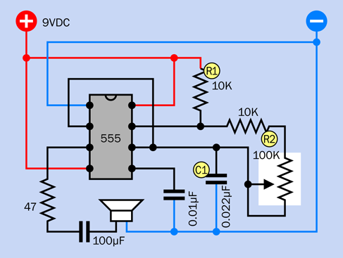
Figure 4-23. This test circuit allows you to adjust the performance of the timer in astable mode.
Now what happens when you apply power? Immediately, you should hear noise through the loudspeaker. If you don’t hear anything, you almost certainly made a wiring error.
Notice that you don’t have to activate the chip with a pushbutton anymore. The 555 timer is triggering itself, as predicted.
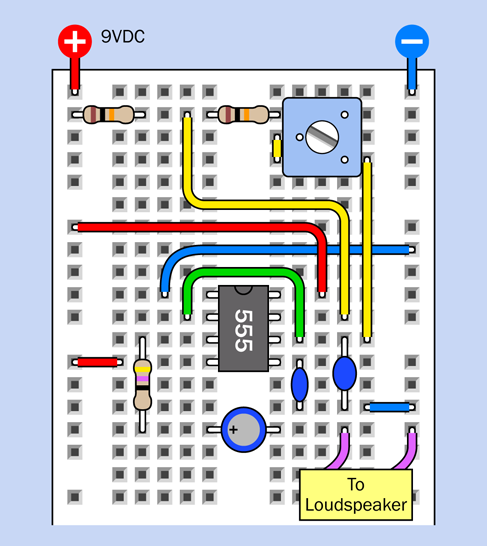
Figure 4-24. Breadboard layout for the astable timer test.
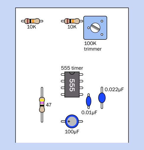
Figure 4-25. Component values for the astable timer test.
Rotate the screw on the trimmer potentiometer, and the pitch of the sound varies. The trimmer adjusts how quickly C1 charges and discharges, and this determines the length of one “on” cycle relative to the next “off” cycle in the audio signal. With these component values, the stream varies between approximately 300 and 1,200 pulses each second. These pulses are sent by the timer to the loudspeaker. They move its cone up and down, creating pressure waves in the air, and your ear responds to those waves, hearing them as sound.
Theory: Output Frequency
The frequency of a sound is its number of full cycles per second, including the high-pressure pulse and the low-pressure pulse that follows.
The term hertz is a unit of frequency, meaning the same thing as “cycles per second.” It was introduced in Europe, named after yet another electrical pioneer, Heinrich Hertz. The abbreviation for hertz is Hz, so the output of your 555 timer in its test circuit will range approximately between 300Hz and 1,200Hz.
As in most standard units, a k can be inserted to mean “kilo,” so 1,200Hz is normally written as 1.2kHz.
How do the values for the timing capacitor and the resistors determine the frequency of the timer? If R1 and R2 are measured in kilohms, and C1 is measured in microfarads, the frequency f, in hertz, is given by:
f = 1,440 / ( ( ( 2 × R2 ) + R1 ) × C1 )
Doing this calculation is a hassle, so I have provided you with a lookup table in Figure 4-26. In this table, I am assuming that the value for the resistor labeled R1 in the schematic is fixed at 10K. The values across the top of the table are for R2. The values on the left side of the table are for the timing capacitor, C1.
You may remember than the abbreviation pF means “picofarad,” which is one-millionth of a microfarad. Nanofarads are halfway between microfarads and picofards, but the term is not used so frequently in the US, so I didn’t use it in the table.

Figure 4-26. For a 555 timer running in astable mode, values across the top refer to R2 in a standard circuit, so long as R1 has a fixed value of 10K. Numbers in the table show the frequency of the timer in Hz (cycles per second).
Theory: Inside the 555 in Astable Mode
To gain a better understanding of what happens when the timer runs in astable mode, take a look at Figure 4-27. The internal configuration is exactly the same as in monostable mode, but the external connections are different.
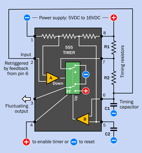
Figure 4-27. Internal view of the 555 timer with external connections running it in astable mode.
Initially, the flip-flop grounds C1, the timing capacitor, as before. But now the low voltage on the capacitor is connected from pin 6 to pin 2 through an external wire. The low voltage tells the chip to trigger itself. The flip-flop obediently flips to its “on” position and sends a positive pulse to the loudspeaker, while removing the negative voltage from pin 6.
Now C1 starts charging, as it did when the timer was in monostable mode, except that it is being charged through R1 + R2 in series. Because C1 has a low value, it charges quickly. When it reaches two-thirds of full voltage, comparator B takes action as before, discharging the capacitor and ending the output pulse from pin 3.
The capacitor discharges through R2 to pin 7, the discharge pin. While the capacitor is discharging, its voltage diminishes. The voltage is still linked to pin 2. When it drops to one-third of full power or less, comparator A kicks in and sends another pulse to the flip-flop, starting the process all over again.
Fundamentals: Unequal On-Off Cycles
When the timer is running in astable mode, C1 charges through R1 and R2 in series. But when C1 discharges, it dumps its voltage into the chip through R2 only. Because the capacitor charges through two resistors but discharges through only one of them, it charges more slowly than it discharges. While it is charging, the output on pin 3 is high; while it is discharging, the output on pin 3 is low. Consequently the “on” cycle is always longer than the “off” cycle. Figure 4-28 shows this as a simple graph.

Figure 4-28. High pulses are always longer than gaps between them in the output from a 555 timer chip, when the chip is wired in the standard way for astable operation.
If you want the on and off cycles to be equal, or if you want to adjust the on and off cycles independently (for example, because you want to send a very brief pulse to another chip, followed by a longer gap until the next pulse), all you need to do is add a diode, as shown in Figure 4-29. (Because a diode deducts some voltage, this circuit works best with a supply voltage greater than 5VDC.)
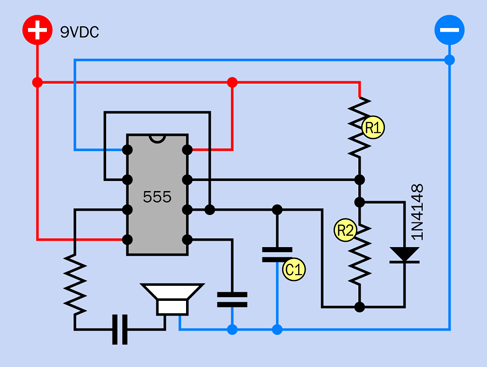
Figure 4-29. Adding a diode to bypass R2 allows the high and low output cycles of a timer to be adjusted independently.
Now when C1 charges, the electricity flows through R1 as before but takes a shortcut around R2, through the diode. When C1 discharges, the diode blocks the flow of electricity in that direction, and so the discharge goes back through R2.
R1 now controls the charge time on its own, while R2 controls the discharge time. The formula for calculating the frequency is now approximately:
Frequency = 1,440 / ( ( R1 + R2 ) × C1 )
where R1 and R2 are in kilohms and C1 is in microfarads. (I use the word “approximately” because the diode adds a small amount of effective resistance to the circuit, which is not factored into the formula.)
If you set R1 = R2, you should get almost equal on/off cycles.
Astable Modifications
Instead of using a potentiometer to vary the value of R2, the frequency of the timer can be changed to a limited extent by using pin 5, the control pin. This is shown in Figure 4-30.

Figure 4-30. A circuit that demonstrates the function of pin 5, the control pin, on the 555 timer.
Disconnect the capacitor that was attached to that pin and substitute the series of resistors shown. They ensure that pin 5 always has at least 1K between it and the positive side or the negative side of the power supply. Connecting it directly to the power supply won’t damage the timer, but will prevent it from generating audible tones. As you turn the potentiometer, the frequency will vary. This happens because you are changing the reference voltage on comparator B inside the chip.
Chaining Chips
Timer chips can be chained together in four possible ways. Note that these configurations are workable regardless of whether each timer is running in monostable or astable mode, except where noted.
-
If you are using 9V to power a 555 timer, the output from that timer can be sufficient to power another 555 timer.
-
The output from one timer can trigger the input of another timer. This only works if the second timer is running in monostable mode. In astable mode, it would be self-triggering.
-
The output from one timer can unlock the reset pin of another timer.
-
The output from one timer can be connected through a suitable resistor to the control pin of another timer.
These options are illustrated in Figure 4-31, Figure 4-32, Figure 4-33, and Figure 4-34.
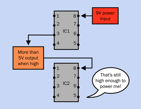
Figure 4-31. One timer powering another.
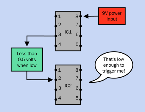
Figure 4-32. One timer triggering another.
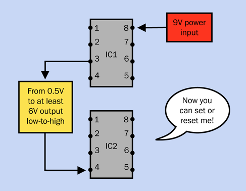
Figure 4-33. One timer setting or resetting another.
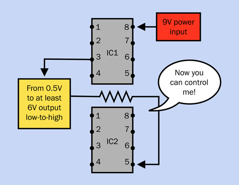
Figure 4-34. One timer controlling the frequency of another.
Why would you want to chain timers together? Well, you might want to have a couple of them running in monostable mode, so that the end of a high pulse from the first one triggers the start of a high pulse in the second one, and vice versa. In fact, you could chain together as many timers as you like, with the last one feeding back and triggering the first one, and they could flash a series of LEDs in sequence, like Christmas lights.
Figure 4-35 shows four timers chained in this way. They are linked through coupling capacitors, because we only want a brief pulse from one to trigger the next. Without the capacitors, the end of the pulse from the first timer in the chain would trigger the second timer, but the output from the first timer would remain in its low state, which would continue triggering the second timer indefinitely.
In addition, each timer must have a 10K pullup resistor on its trigger pin to hold it normally high.
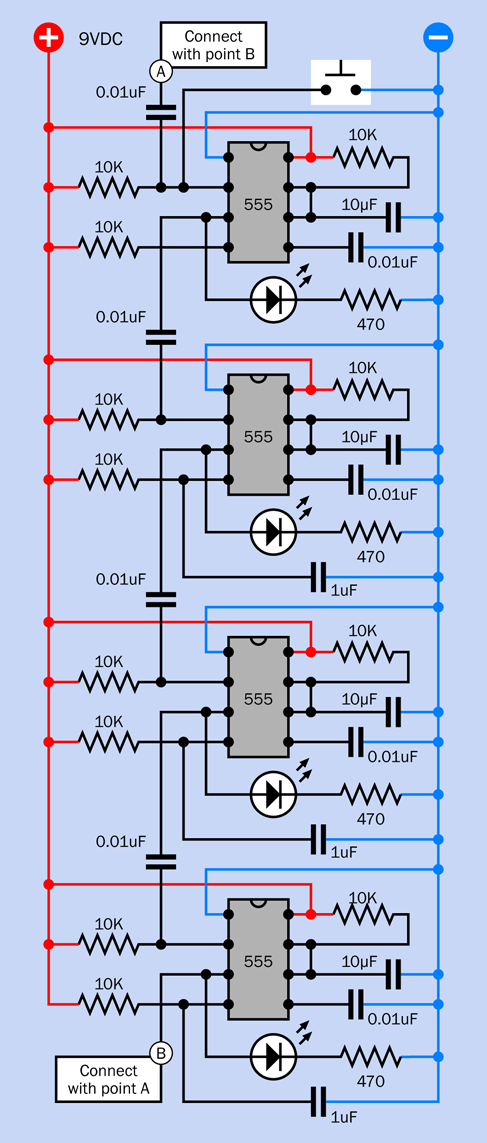
Figure 4-35. Four timers wired to trigger each other in a recirculating sequence.
An interesting question comes to mind when monostable timers are chained together. That is: how do they start? I mentioned in Experiment 16 that a 555 timer in monostable mode will usually emit one spontaneous pulse when it is first powered up. When multiple timers are chained together, they will all try to do this at about the same time, and because of small manufacturing differences, the outcome will be unpredictable. Sometimes they will settle down to a nice orderly sequence, but other times they will end up flashing in pairs.
The way to deal with this is to use the concept of pulse suppression that I mentioned in Experiment 16 (see “Fundamentals: Pulse Suppression”).
A 1µF capacitor between the reset pin and negative ground will hold the reset pin in a low state just long enough to suppress the timer’s initial pulse. A 10K pullup resistor sharing the reset pin will then keep it stable while the timer is running.
In my experience, this works well, although timers from a different manufacturer could conceivably behave differently, as the behavior of the reset pin is not well documented. If you have trouble with pulse suppression, try substituting a larger or smaller capacitor.
In a chain of timers, the only remaining problem is that pulse suppression works too well. You apply power, and—nothing happens, because all the timer outputs have been suppressed.
The way around this is to omit pulse suppression from just one timer. It will almost certainly emit an initial pulse when it receives power, and that will trigger the rest in sequence. This setup is illustrated in Figure 4-35.
But—wait a minute. What is this “almost certainly” phrase? Electronic circuits should always work, all the time, not “almost” all the time.
I agree. But I can’t control the tendency of 555 timers to do unpredictable things when they are powered up. Therefore I also added a button, at the top of the circuit, that can be used to start the cascade if it doesn’t start itself.
There is an alternative, which is for the first timer in the chain to run in astable mode. It sends a series of pulses that ripple down through the others configured in monostable mode, and the last one does not feed back to the first. In electronics terms, we say that the first one is the master and the others are the slaves.
I like this arrangement because it is totally predictable. The trouble is, you have to adjust the speed of the master timer so that it emits its next pulse exactly when the last slave in the chain has just finished emitting its pulse. Otherwise, the first timer will emit another pulse before the last pulse has ended, or there will be a gap between the last pulse and the next first pulse.
Whether this is important will depend on the application. Flashing lights won’t be a problem, but if you increase the speed to drive a stepper motor, getting the timing right will be difficult.
Sounding Like a Siren
The fourth option that I listed for chaining chips, in Figure 4-34, is of special interest, because it can create a siren sound very like the noise made by a typical burglar alarm. In fact, this could be used for the audio output in the alarm project that I left unfinished in Experiment 15.
The circuit is shown in Figure 4-36. Timer 1 is wired in a basic astable circuit, which you can recognize as being similar to the circuit in Figure 4-22. The component values are larger, so the timer oscillates more slowly, around 1Hz. You can compare this circuit with the one that I suggested in Figure 2-120. The principle is similar.
Timer 2 is also wired in a basic astable circuit, running around 1kHz. The idea is that the slow fluctuations in voltage from Timer 1 are applied to the control pin of Timer 2, forcing it to modulate its sound up and down in that annoying way which we associate with alarm systems.
I encourage you to build this circuit, because you may want to use it in the final version of the intrusion alarm coming right up in Experiment 18. The breadboard layout for the siren circuit is in Figure 4-37, and the component values for the layout are shown in Figure 4-38.
Once you get it running, you may find it interesting to remove and then replace the 100µF capacitor connected between pin 6 and ground. The capacitor makes the frequency slide higher and lower instead of switching sharply up and down. I’m using it in the same way that I used a capacitor to make an LED fade smoothly in and out in Experiment 11.
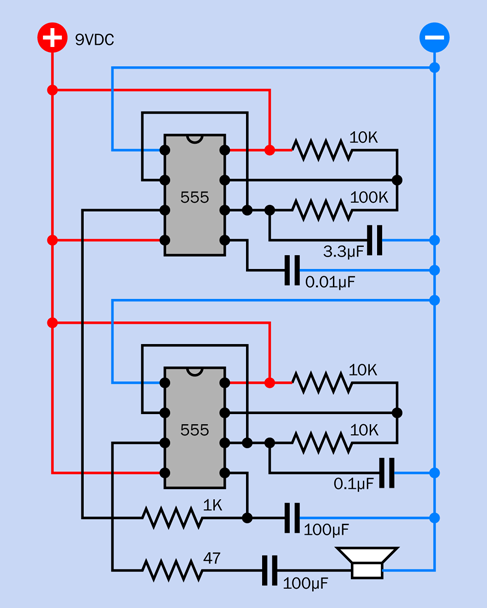
Figure 4-36. When one timer runs relatively slowly, modulating another through its control pin (pin 5), the result is a wavering sound like an alarm siren.
You can modify the sound in other ways. Here are some suggestions:
-
Vary the 0.1µF timing capacitor to raise or lower the pitch of the basic sound.
-
Double the value of the 100µF capacitor on pin 6, or divide it by two.
-
Substitute a 10K potentiometer for the 1K resistor.
-
Change the value of the 3.3µF capacitor.
Part of the pleasure of building things is to customize them, to make them your own. Once your siren sound satisfies you, make a note of the component values for future reference.
Incidentally, you can reduce the chip count (the number of chips) by using a 556 timer instead of two 555 timers. The 556 contains a pair of 555 timers in one package. Because you still have to make the same number of external connections (other than the power supply), I haven’t bothered to use this variant.
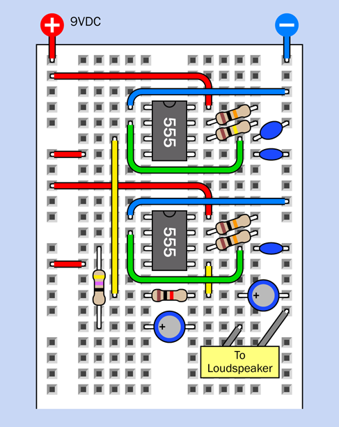
Figure 4-37. The siren circuit, breadboarded.
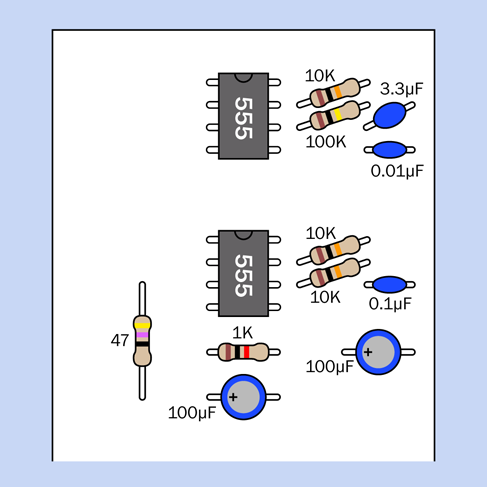
Figure 4-38. Component values for the siren circuit.
Experiment 18: Intrusion Alarm (Almost) Completed
Now that you’ve seen what the 555 timer can do, you can fulfill the remaining requirements on the intrusion-alarm wish list.
What You Will Need
-
Breadboard, hookup wire, wire cutters, wire strippers, multimeter
-
9-volt power supply (battery or AC adapter).
-
555 timers (2)
-
DPDT 9VDC relay (1)
-
Transistors, 2N2222 (2)
-
LEDs: Red, green, yellow (1 of each)
-
Slide switch, SPDT, for breadboard (2)
-
Tactile switch (1)
-
Capacitors: 0.01µF (1), 10µF (2), 68µF (2)
-
Resistors: 470 ohms (4), 10K (4), 100K (1), 1M (2)
-
Diode, 1N4001 (1)
Optional (for audio output):
-
Components shown in Figure 4-36
Optional (for permanent fabrication of this project):
-
15-watt soldering iron
-
Thin solder
-
Perforated board plated with copper in a breadboard layout
-
SPDT or DPDT toggle switch (1)
-
Pushbutton, SPST (1)
-
Project box, at least 6” × 3” × 2” (1)
-
Power jack and matching power socket (1 each)
-
Magnetic sensor switches, in pairs, quantity sufficient for your home
-
Alarm network wiring, sufficient for your home
Three Steps to a Functional Device
This is a larger and more complicated circuit than anything you have tackled so far, but it’s relatively easy to build, because you can assemble it in three parts that you can test individually. Eventually you’ll end up with a breadboard looking like Figure 4-45, with component values in Figure 4-46. The equivalent schematic is shown in Figure 4-47. But we’ll begin with just a small timer circuit.
Step 1
Take a careful look at Figure 4-39. Notice there are no timing components on the righthand side of the 555 timer. You may conclude that this is a version of the bistable circuit that I described in Experiment 16 (see Figure 4-20). When the timer is triggered, its output will go on indefinitely—which seems appropriate for an alarm system.
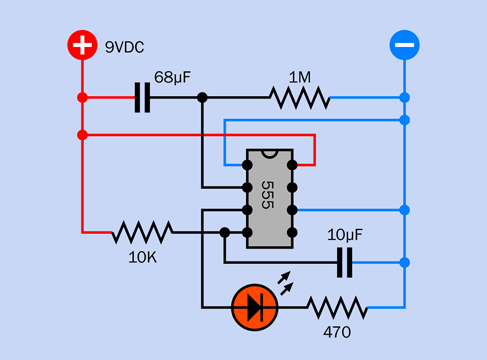
Figure 4-39. Schematic equivalent of the bottom section of the breadboard layout.
But there’s more to it than that. This circuit also gives you a one-minute grace period in which to disable the alarm before it starts to sound, when you enter the area. (You may remember that this was #9 on the wish list of features that I compiled in Experiment 15.)
To see how it works, you can assemble the components shown in Figure 4-40. Their values are shown in Figure 4-46, and you’ll see their placement at the bottom of the board in Figure 4-45.
The placement is important, because you have to leave room for the additional sections of the circuit that you’ll be adding. One of those sections will be switching on the power to this one.
To make sure that you have everything in the right place, the 1M resistor on the right is on the 29th row in the board, counting down from the top. Also note that power is being applied near the components, not at the top of the board, and the positive bus is not being used, yet.
Don’t power up the circuit just yet. Set your meter to measure at least 10VDC and attach it at the points shown in Figure 4-40, with the negative probe on the negative bus and the positive probe at the left end of the 1M resistor.
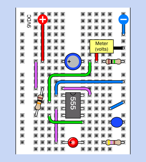
Figure 4-40. Placement of components at the bottom of the breadboard for testing.
Now apply power to the circuit, and you should see your meter slowly counting down from 9V. When it gets to one-third of the supply voltage, this triggers the 555 timer, and the red LED comes on. The LED is included for testing purposes; in the final version, you would substitute a noisemaking circuit.
The large 68µF capacitor delays the response of the timer. When you first apply power to the circuit, the capacitor passes the initial pulse to the point between it and the 1M resistor. The green wire runs from this point to the trigger pin of the timer. So, the pin starts off high, and you’ll remember (I hope) that the timer does nothing until the trigger pin goes low.
Voltage on the righthand side of the capacitor leaks out very slowly through the 1M resistor. Eventually, it goes low enough to trigger the timer.
As for the rest of the circuit, in Experiments 16 and 17 I explained how to do “pulse suppression” to stop the timer from emitting a pulse when it is first powered up. This is why I have a 10µF capacitor and a 10K resistor applied to pin 4, the reset pin. I’m using a 10µF capacitor this time, instead of a 1µF capacitor, because this circuit reacts a bit more slowly than the one in Experiment 17.
-
You can use a 555 timer with these components any time you want to delay the timer output in response to a trigger pulse.
-
Use a larger or smaller value for the 68µF capacitor if you want to make the delay longer or shorter.
So far, so good. This part of the circuit will introduce a delay when it is powered up, and after the delay, it will activate the alarm for an indefinite period.
Step 2
Figure 4-41 and Figure 4-42 show the next step in building the circuit. The components that you placed previously are still there, but they have been grayed out to focus your attention on the new additions.
Don’t forget to install S2, the slide switch at the bottom, and the 470-ohm resistor beside it, and the two long yellow wires. This slide switch is included for testing purposes. It represents the alarm sensors that you would use in an actual application.
The relay has the same function as in Experiment 15. In fact if you trace the connections in the circuit, you’ll find that it works the same way as the one in Figure 3-88, with a couple of minor revisions. The only differences are that a 470-ohm resistor has been substituted for a 1K resistor, and I have added switch S1 at the top, with a green LED. Why? I’ll get to that in a moment.
Place all the components carefully. Don’t overlook the three red wires on the left and the three blue wires on the right. Make sure the pins of the relay are aligned with the wires that serve them.
Double-check that S1 is in the down position, and S2 is in the up position. For testing purposes, remove the 68µF capacitor so that the red LED will respond right away instead of waiting for a minute.
Attach power—and if you made all the connections correctly, nothing should happen. Switch S2 represents the alarm sensors, and in its up position, it simulates them being closed. Slide it down to simulate a sensor being opened, and the test LED at the bottom of the circuit should light up immediately. Slide the switch up, and the LED stays on. The circuit has locked the alarm on, regardless of a sensor being reset.
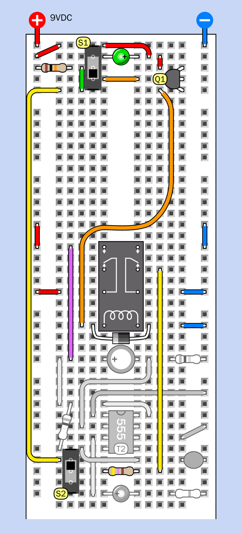
Figure 4-41. The second step in building this circuit incorporates the relay configuration that was used in Experiment 15.
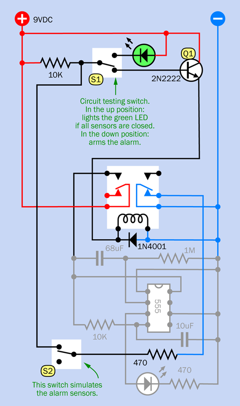
Figure 4-42. Schematic equivalent of the breadboarded second stage in the circuit.
Disconnect the power, keep S2 in its up position (simulating the sensors being closed), and reapply the power. Now move S1, at the top, to its up position, and the green LED comes on. This is a circuit-testing feature. It checks that all the sensors are closed. When you use the alarm, you will want to conduct this test before you leave the area. This satisfies the first part of item #7 in the wish list from Experiment 15.
Keep S1 in its up position while you move S2 to its down position, to simulate an open sensor. The green LED goes out. Move S2 to its up position, and the green LED comes back on. So, the testing procedure works.
Here’s how you would actually use this circuit. You leave S1 in the up (test) position. When you are ready to leave the area, you apply power to the circuit. If the green LED doesn’t come on, there is a door or window open somewhere. Find the source of the problem, and correct it. When the green LED is on, you know that all the sensors are closed. Now you can arm the alarm. Move S1 down. The green LED goes out, and the alarm is now armed. When you come home, the 555 timer gives you one minute to disable the alarm, to prevent it from going off (so long as you have replaced the 68µF capacitor in the circuit). You can disable the alarm by moving S1 to its up (test) position.
Now, how and why does the circuit work?
The 10K resistor at top-left connects with the base of transistor Q1 through switch S1, when the switch is in its down position. Meanwhile, the righthand pole contact inside the relay is connected to negative ground. This connection runs through the yellow wire on the right, through a 470-ohm resistor, through switch S2 (which simulates the sensors), and back up through the other long yellow wire. It holds the base of the resistor at a low voltage (through the orange wire). So long as the base is low, the transistor doesn’t conduct.
If a sensor opens, the base of the transistor isn’t held low anymore, and the 10K resistor pulls it up so that the transistor starts to conduct. It triggers the relay, through the long curving orange wire. The relay will supply power to the bistable timer, which will eventually activate the alarm. At the same time, the relay breaks the negative-ground connection on the right, so now the transistor is going to continue conducting even if the sensor is closed again.
This is exactly the same circuit concept that I ended up with in Figure 3-88. The significant difference is the green LED. When you move S1 to its “test” position, it cuts off positive power to the transistor (so that the transistor cannot start the alarm). If all the sensors are closed, the LED connects through them, and the 470-ohm resistor, to negative ground, and it lights up to tell you that the system is ready.
Step 3
What else could we need in this project? Well, imagine you are using the alarm system. You want to set it before leaving the area. At this point, you suddenly realize that if you set it, and then open a door to leave, you will trigger the alarm.
The bistable timer with its 68µF capacitor added a feature to suppress the alarm for a minute, to give you time to turn it off when you arrive. Now we need another timer to suppress the alarm for a minute when you leave.
This is a little more difficult to arrange. The key is to have the extra timer pull down the voltage on transistor Q1, so that it can’t trigger the relay.
The problem is, a timer output goes high, not low, during its “on” cycle. I’ll have to add another transistor to convert the high output so that it pulls down the voltage on the base of transistor Q1.
Figure 4-43 and Figure 4-44 show the components that will make it happen. Once again I have grayed out the components that you placed previously.
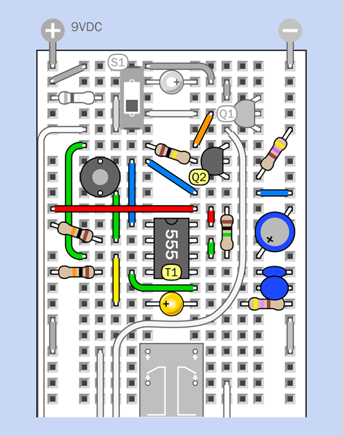
Figure 4-43. Third and final step in building the alarm circuit.
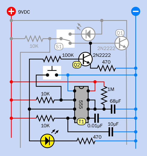
Figure 4-44. The schematic version of the third step in building the circuit.
The new 555 timer, labeled T1, has a pulse-suppression circuit on pin 4, its reset pin, like the other timer, so that it won’t emit a pulse when you power up the circuit. You press the button to start T1. The button works by grounding the trigger pin of the timer.
While the output of the timer is high, the current flows out of pin 3 (the output pin) and lights up the yellow LED. This tells you that the alarm system is counting down to being armed. So long as you see the LED, the alarm will ignore any activity that opens a sensor switch.
Pin 3 also connects through a green wire, on the left, which is like an elongated letter C. This curls around to a 100K resistor, which is attached to the base of Q2, a second transistor. The output from the timer, through the 100K resistor, is enough to make Q2 conduct. Its emitter is grounded through a 470-ohm resistor, while its collector is attached to the base of Q1. So long as Q2 is conducting, it grounds the base of Q1, and prevents Q1 from triggering the relay and starting the alarm.
In this way, timer T1 stops the alarm from going off. When the one-minute grace period ends, T1 stops conducting, doesn’t pull down the voltage on the first transistor anymore, and the alarm can go off—provided you remembered to move the switch at the top out of “test” mode, of course.
You would now use the circuit like this.
-
First put switch S1 into its “test” position and close all the doors and windows until the green LED comes on.
-
Move S1 into its lower position, so that the alarm is ready.
-
Press the button, and leave, closing the door behind you, while the yellow LED is on.
Does your version do what it is supposed to do? It should, so long as you wired it carefully. Timer T1 should light the yellow LED under any circumstances, making it easy to test. You can also touch your meter probe on the base of Q1, to verify whether the voltage is relatively high or low. So long as the voltage is relatively low, the alarm will not be triggered. When the voltage goes high, the alarm is triggered.
Don’t forget to replace the 68µF capacitor in the circuit, just below the relay, to reactivate the delay timer, when your alarm is ready for prime time.
The complete breadboarded circuit is shown in Figure 4-45, the component values are in Figure 4-46, and the schematic is in Figure 4-47.
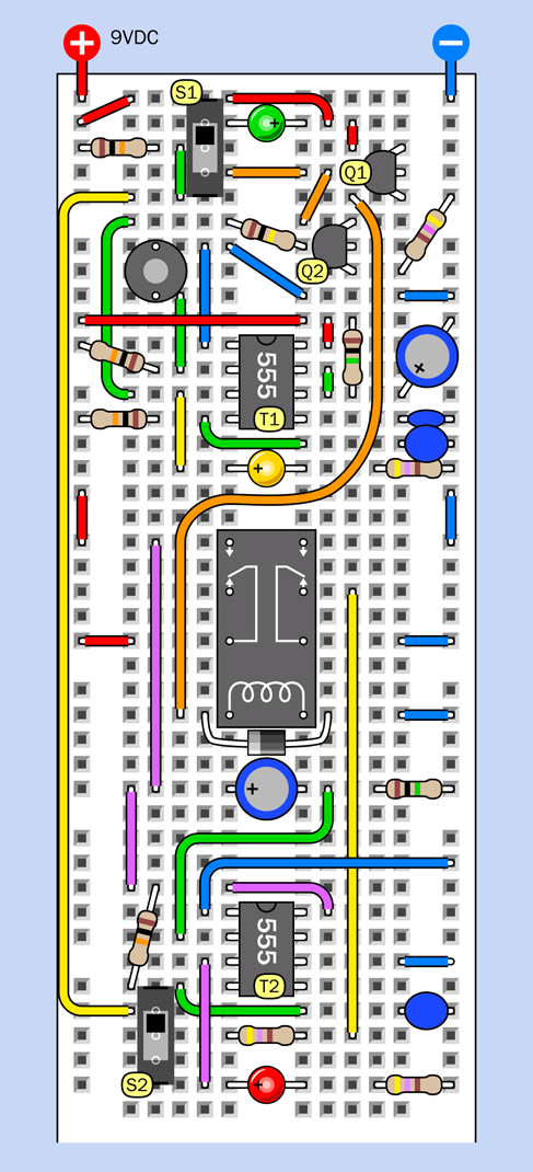
Figure 4-45. Breadboard layout for the complete alarm circuit.
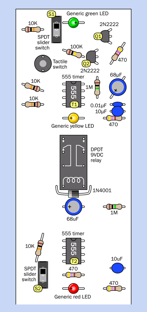
Figure 4-46. Component values in the breadboard layout.
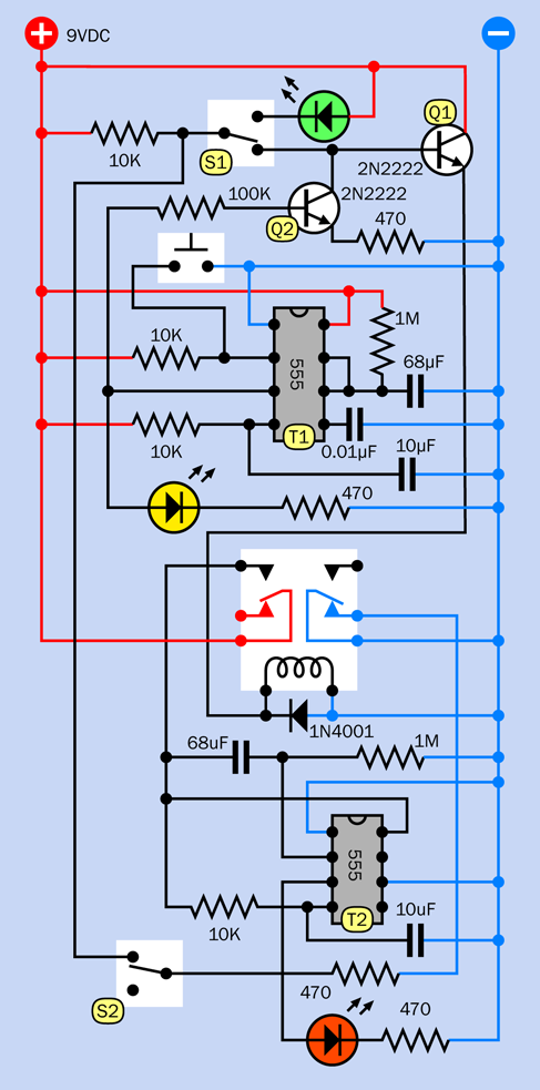
Figure 4-47. Schematic equivalent of the breadboarded alarm circuit.
What About the Noise?
When you want the alarm to make noise, you’ll need to substitute an audio circuit or device for the red LED that you have been using for testing purposes.
The easy way to do this is to use an off-the-shelf item. Hundreds of sirens are available cheaply, ready to make an annoying sound if you simply apply power. Many of them require 12VDC, but they deliver almost as much noise at 9VDC. Just remember that timer T2 cannot deliver much more than 150mA.
If you prefer to have a sound that’s all your own, you can use the circuit that I showed in Figure 4-36. Just use the output from your relay to power this circuit, and you have your own sound.
What About On and Off?
You’ve been testing the circuit by applying and removing power. You can add an on-off switch, but a numeric code to switch off the alarm would be more desirable.
Right now, I can’t show you how to implement that, because it requires logic chips that I have not dealt with yet. But Experiment 21 will show you how it can be done.
Finalizing
Meanwhile, since the alarm circuit does actually work in its current form, I want to talk about finalizing it. By this I mean soldering it to a board, mounting the board in a box, and making everything look nice. My main concern in this book is electronics, but still, finalizing a project is an important part of the making experience, so I’ll give you some suggestions.
Soldering the circuit can be easier than the procedure in Experiment 14, where I explained point-to-point wiring. You can mount the components on the type of perforated board that has copper traces on the back, in a configuration identical to the connectors inside a breadboard. Simply move each component to its comparable position, and solder it to the copper conductor underneath. No wire-to-wire soldering is necessary.
Guidance for finding and buying this kind of board is in “Supplies” near the end of the book.
Now, how to proceed:
Carefully note the position of a component on your breadboard, then move it to the same relative position on the perforated board, poking its wires through the little holes.
Turn the perforated board upside down, make sure that it’s stable, and examine the hole where the wire is poking through, as shown in Figure 4-48, which shows the underside of the board (the component is on the other side). A copper trace surrounds this hole and links it with others. Your task is to melt solder so that it sticks to the copper and also to the wire, forming a solid, reliable connection between the two of them.
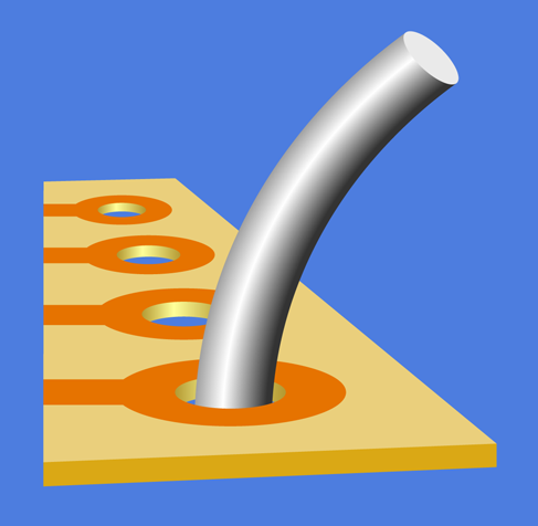
Figure 4-48. The underside of perforated board, with a wire sticking through.
Clamp the perforated board or rest it on a surface where it won’t skid around easily. Take your low-wattage soldering iron in one hand and some solder in your other hand. Hold the tip of the iron against the wire and the copper, and feed some thin solder to their intersection. After two to four seconds, the solder should start flowing.
Allow enough solder to form a rounded bump sealing the wire and the copper, as shown in Figure 4-49. Wait for the solder to harden thoroughly, and then grab the wire with pointed-nosed pliers and wiggle it to make sure you have a strong connection. If all is well, snip the protruding wire with your cutters. See Figure 4-50.

Figure 4-49. Ideally, your solder joint should look something like this.
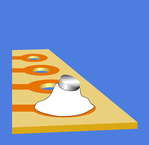
Figure 4-50. After the solder has cooled and hardened, you snip off the projecting wire.
Because solder joints are difficult to photograph, I’m using drawings to show the wire before and after making a reasonably good joint. The solder is shown in pure white, outlined with a black line.
The process of actually soldering components into perforated board is illustrated in Figure 4-51 and Figure 4-52.
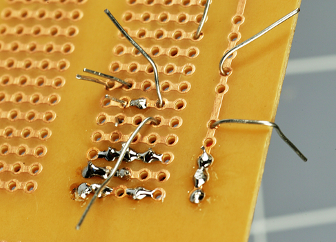
Figure 4-51. This photograph was taken during the process of transferring components from breadboard to perforated board. Two or three components at a time are inserted from the other side of the board, and their leads are bent over to prevent them from falling out.

Figure 4-52. After soldering, the leads are snipped short and the joints are inspected under a magnifying glass. Another two or three components can now be inserted, and the process can be repeated.
Most Common Perfboarding Errors
1. Too much solder. Before you know it, solder creeps across the board, touches the next copper trace, and sticks to it, as depicted in Figure 4-53. When this happens, you can either try to suck it up with a desoldering kit, or carve it away with a knife. Personally I prefer to use a knife, because if you suck it up with a rubber bulb or solder wick, some of it will tend to remain.

Figure 4-53. If you use too much solder, it will tend to end up in places where you don’t want it.
Even a microscopic trace of solder is enough to create a short circuit. Check the wiring with a magnifying glass while turning the perforated board so that the light strikes it from different angles.
2. Not enough solder. If the joint is thin, the wire can break free from the solder as it cools. Even a microscopic crack is sufficient to stop the circuit from working. In extreme cases, the solder sticks to the wire, and sticks to the copper trace around the wire, yet doesn’t make a solid bridge connecting the two, leaving the wire encircled by solder yet untouched by it, as shown in Figure 4-54. You may find this undetectable unless you observe it with magnification.
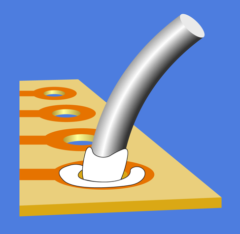
Figure 4-54. Too little solder (or insufficient heat) can allow a soldered wire to remain separate from the soldered copper on the perforated board. Even a hair-thin gap is sufficient to prevent an electrical connection.
You can add more solder to any joint that may have insufficient solder, but be sure to reheat the joint thoroughly.
3. Components incorrectly placed. It’s very easy to put a component one hole away from the position where it should be. It’s also easy to forget to make a connection.
I suggest that you print a copy of the schematic, and each time you make a connection on the perforated board, you eliminate that wire on your hardcopy, using a highlighter.
4. Debris. When you’re trimming wires, the little fragments that you cut don’t disappear. They start to clutter your work area, and one of them can easily get trapped under your perforated board, creating an electrical connection where you don’t want it.
Clean the underside of your board with an old toothbrush before you apply power to it. Dip the toothbrush in rubbing alcohol to remove flux residues. Keep your work area as neat as possible. The more meticulous you are, the fewer problems you’ll have later.
Once again, be sure to check every joint with a magnifying glass.
Fundamentals: Perforated Board Fault Tracing
If the circuit that worked on your breadboard doesn’t work after you solder it to perforated board, your fault tracing procedure is a little different from that which I outlined previously.
First look at component placement, because this is the easiest thing to verify.
If all the components are placed correctly, flex the board gently while applying power. If you now get an intermittent response from the circuit, you can be virtually certain that solder didn’t stick where it was supposed to stick, or a joint has a tiny crack in it.
Anchor the black lead of your meter to the negative side of the power supply, then switch on the power and go through the circuit point by point, from top to bottom, checking the voltage at each point with the red lead of the meter while you continue to flex the board. In most circuits, almost every part should show at least some voltage. If there is a dead zone, or if your meter responds intermittently, you can zero in on a joint that has something wrong with it, even though it looks good superficially.
A bright desk lamp and a magnifier are indispensable for this procedure. A gap of 1/1,000” or less is quite sufficient to stop your circuit from working. But you’ll have difficulty detecting it without magnification, and even then, sometimes the light has to be exactly right.
Dirt, water, or grease can prevent solder from sticking properly to wires or copper traces. This is just another reason to be as meticulous as possible in your work habits.
The Project Box
The easiest way to enclose your perforated board is to put it in a project box. (I mentioned this item in the list of components and supplies at the beginning of Chapter 3). Hundreds of variants are available. Aluminum boxes look cool and professional, but you have to protect the circuit board from short-circuiting itself on the inside of the box. Plastic boxes are easier, and cheaper, too.
To make everything look professional, you should not just start drilling holes arbitrarily for your switches and LEDs. You should draw a layout on paper (or use a drawing program, and then print the image on paper). Just make sure there’s room for the components to fit together, and try to place them similarly to the schematic, to minimize the risk of confusion.
Tape your sketch to the inside of the top panel, as shown in Figure 4-55, and then use a sharp, pointed tool (such as an awl or a needle) to press through and mark the plastic at the center of each hole. The indentations will help to center your bit when you drill the holes.
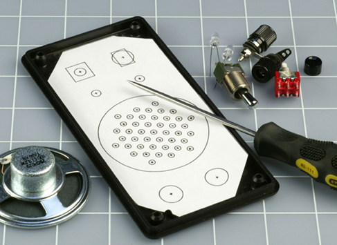
Figure 4-55. A printed layout for the switches, LEDs, and other components has been taped to the underside of the lid of the project box. An awl is pressed through the paper to mark the center of each hole to be drilled in the lid.
If you’re using an audio circuit driving a loudspeaker (instead of a ready-made siren) you’ll need to make multiple holes to vent the sound from the loudspeaker, which will be beneath the top panel of the box. The panel that I made is shown in Figure 4-56.
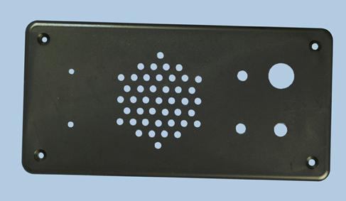
Figure 4-56. The exterior of the panel after drilling. A small handheld cordless drill can create a neat result if the holes were marked carefully.
I placed all the switches and LEDs on the top panel. The power input jack is positioned at one end of the box. Naturally, each hole has to be sized to fit its component, and if you have calipers, they’ll be very useful for taking measurements and selecting the right drill bit. Otherwise, make your best guess, too small being better than too large. A deburring tool is ideal for slightly enlarging a hole so that a component fits snugly. This may be necessary if you drill 3/16-inch holes for your 5-inch mm LEDs. Fractionally enlarge each hole, and the LEDs should push in very snugly.
If your loudspeaker lacks mounting holes, you’ll have to glue it in place. I used five-minute epoxy to do this. Be careful not to use too much. You don’t want any of the glue to touch the speaker cone.
Drilling large holes in the thin, soft plastic of a project box can be a problem. The drill bit tends to dig in and create a mess. You can approach this problem in one of three ways:
-
Use a Forstner drill bit if you have one. It creates a very clean hole. A hole saw can also be used.
-
Drill a series of holes of increasing size.
-
Drill a smaller hole than you need, and enlarge it with a deburring tool.
Regardless of which approach you use, you’ll need to clamp or hold the top panel of the project box with its outside surface face-down on a piece of scrap wood. Then drill from the inside, so that your bit will pass through the plastic and into the wood.
Finally, mount the components in the panel, as shown in Figure 4-57, and turn your attention to the underneath part of the box.
Soldering the Switches
Your first step is to decide which way up the switch should be. Use your meter to find out which terminals are connected when the switch is flipped. You’ll probably want the switch to be on when the toggle is flipped upward. The underside of my control panel is shown in Figure 4-57. I used a DPDT switch because I just happened to have one. You only need a SPST switch for the project.
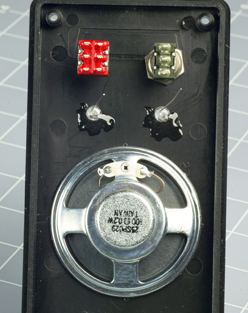
Figure 4-57. Components have been added to the control panel of the project box (seen from the underside). The loudspeaker has been glued in place. Spare glue was dabbed onto the LEDs, just in case.
Remember, the center terminal of any double-throw switch is almost always the pole of the switch.
Stranded wire is appropriate to connect the circuit board with the components in the top panel, because the strands flex easily and impose less stress on solder joints. Twisting each pair of wires together helps to minimize the mess.
When you connect wires or components with the lugs on the switches, your pencil-style soldering iron may not deliver enough heat to make good joints. You can use your higher-powered soldering iron in these locations, but you absolutely must apply a good heat sink to protect the LEDs when you attach them, and don’t allow the iron to remain in contact with anything for more than 10 seconds. It will quickly melt insulation, and may even damage the internal parts of the switches.
In projects that are more complex than this one, it would be good practice to link the top panel with the circuit board more neatly. Multicolored ribbon cable is ideal for this purpose, with plug-and-socket connectors that attach to the board. For this introductory project, I didn’t bother. The wires just straggle around, as shown in Figure 4-58.
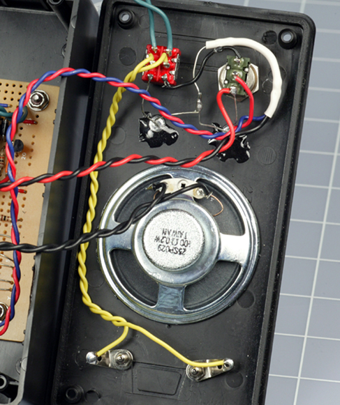
Figure 4-58. Twisted wire pairs have been connected on a point-to-point basis, without much concern over neatness, as this is a relatively small project.
Fixing the Board
The circuit board will sit on the bottom of the box, held in place with four #4-size machine screws (bolts) with washers and nylon-insert locknuts. I prefer using nuts and bolts, rather than glue, in case I ever need to remove the circuit to make a repair. You need to use locknuts to eliminate the risk of a nut working loose and falling among components, where it can cause a short circuit.
You’ll have to cut the perforated board to fit, taking care not to damage any of the components on it. I use a band saw for cutting, but a hacksaw will work. Remember that perforated board often contains glass fibers that can blunt a wood saw.
Check the underside the board for loose fragments of copper traces after you finish cutting.
Drill bolt holes in the board, taking care again not to damage any components. Then mark through the holes to the plastic bottom of the box, and drill the box. Countersink the holes (i.e., bevel the edges of a hole so that a flat-headed screw will fit into it flush with the surrounding surface), push the little bolts up from underneath, and install the circuit board. Because you’re using locknuts, which will not loosen, there’s no need to make them especially tight. Indeed, excessive tightness must be avoided.
After mounting the board, test the circuit again, just in case.
Caution: Avoid Board Stress
Be extremely careful not to attach the circuit board too tightly to the project box. This can impose bending stresses, which may break a joint or a copper trace on the board.
Final Test
When you’ve completed the circuit, if you don’t have your network of magnetic sensor switches set up yet, you can just use a piece of wire instead. I used a pair of binding posts on my box, just for convenience. You can equally well run a pair of wires from the circuit board out through a small hole in the lid of the box.
If everything works the way it should, it’s time to screw the top of the box in place, pushing the wires inside. Because you’re using a large box, you should have no risk of metal parts touching each other accidentally, but still, proceed carefully. My finished product is shown in Figure 4-59.
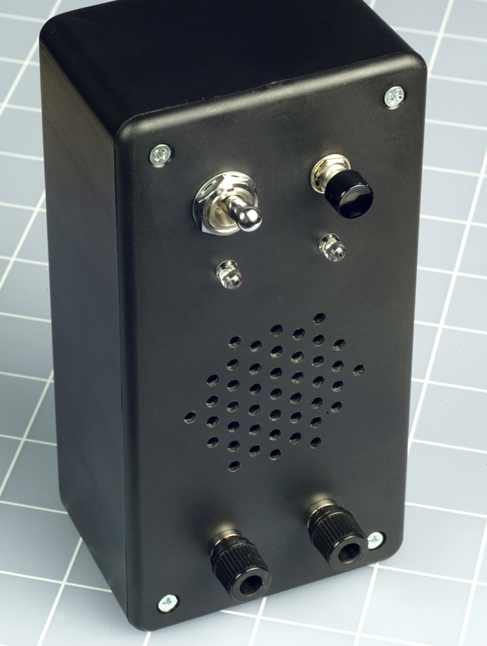
Figure 4-59. The completed alarm box.
Alarm Installation
If you are going to complete this project with magnetic sensor switches, you should test each one by moving the magnetic module near the switch module and then away from it, while you use your meter to test continuity between the switch terminals. The switch should close when it’s next to the magnet, and open when the magnet is removed.
Now draw a sketch of how you’ll wire your switches together. Always remember that they have to be in series, not in parallel! Figure 4-60 shows the concept in theory. The two terminals are the binding posts on top of your control box (which is shown in green), and the dark red rectangles are the magnetic sensor switches on windows and doors. Because the wire for this kind of installation usually has two conductors, you can lay it as I’ve indicated but cut and solder it to create branches. The solder joints are shown as orange dots. Note how current flows through all the switches in series before it gets back to the control box.
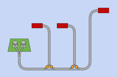
Figure 4-60. Dual-conductor, white insulated wire can be used to connect the terminals on the alarm control box with magnetic sensors (shown in dark red). Because the sensors must be in series, the wire is cut and joined at positions marked with orange dots.
Figure 4-61 shows the same network as you might actually install it in a situation where you have two windows and a door. The blue rectangles are the magnetic modules that activate the switch modules.
You’ll need a large quantity of wire, obviously. The type of white, stranded wire that is sold for doorbells or furnace thermostats is good. Typically, it is 20-gauge or larger.
After you install all the switches, clip your meter leads to the wires that would normally attach to the alarm box. Set your meter to test continuity, and open each window or door, one at a time, to check whether you’re breaking the continuity. If everything is OK, attach the alarm wires to the binding posts on your project box.
Now deal with the power supply. Use your AC adapter, with its output set to 9 volts, hooked up to your DC power plug, or attach the power plug to a 9-volt battery. The circuit will run off a 12-volt alarm battery too, but you will have to substitute a 12-volt relay for the one that I specified.
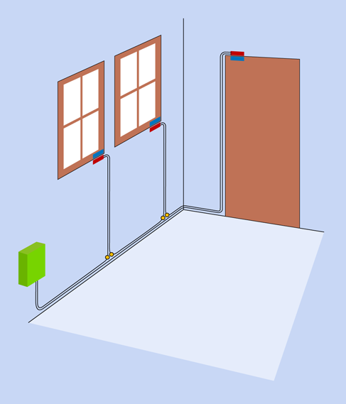
Figure 4-61. In an installation involving two windows and a door, the magnetic components of the sensors (blue rectangles) could be placed as shown, while the switches (dark red) are located alongside them.
The only remaining task is to label the switch, button, power socket, and binding posts on the alarm box. You know that the switch puts the alarm in and out of continuity testing mode, and the button gives you a minute to leave before the system alarms itself, but no one else knows, and you might want to allow a guest to use your alarm while you’re away. For that matter, months or years from now, you may forget some details yourself.
Conclusion
The alarm project has taken you through the basic steps that you will usually follow any time you develop something:
-
Make a wish list.
-
Decide which types of components are appropriate.
-
Draw a schematic and make sure that you understand it.
-
Modify it to fit the pattern of conductors on a breadboard.
-
Install components on the breadboard and test the basic functions.
-
Modify or enhance the circuit, and retest.
-
Transfer to perforated board, test, and trace faults if necessary.
-
Add switches, buttons, a power jack, and plugs or sockets to connect the circuit with the outside world.
-
Mount everything in a box (and add labeling).
Experiment 19: Reflex Tester
Because the 555 timer can run at thousands of cycles per second, you can use it to measure human reflexes. You can compete with friends to see who has the fastest response—and note how your response changes depending on your mood, the time of day, or how much sleep you got last night.
This circuit is not conceptually difficult, but requires quite a lot of wiring, and will only just fit on a breadboard that has 60 rows of holes (or more). Still, it can be tested in sections, like the circuit in Experiment 18. If you avoid making errors, the whole project can be assembled in a couple of hours.
What You Will Need
-
Breadboard, hookup wire, wire cutters, wire strippers, multimeter
-
9-volt power supply (battery or AC adapter)
-
4026B chips (3)
-
555 timers (3)
-
Resistors: 470 ohms (2), 680 ohms (3), 10K (6), 47K (1), 100K (1), 330K (1)
-
Capacitors: 0.01µF (2), 0.047µF (1), 0.1µF (1), 3.3µF (1), 22µF (1), 100µF (1)
-
Tactile switches (3)
-
Generic LEDs: one red, one yellow
-
Trimmer potentiometer, 20K or 25K (1)
-
Single-digit numeric LED displays, height 0.56”, low-current red preferred, able to function at 2V forward voltage and 5mA forward current (3) (Avago HDSP-513A preferred, or Lite-On LTS-546AWC, or Kingbright SC56–11EWA, or similar)
Caution: Protecting Chips from Static
The 555 timer is not easily damaged, but in this experiment you will also be using a CMOS chip (the 4026B counter), which is more vulnerable to static electricity.
Whether you are likely to zap a chip by handling it depends on factors such as the humidity in your location, the type of shoes you wear, and the type of floor covering in your work area. Some people seem to accumulate a charge of static more easily than others, and I don’t have an explanation for this. Personally, I have never damaged a chip with static, but I know people who have.
If static is a risk for you, you’ll probably know about it, because you’ll suffer from sudden little jolts when you reach for a metal door handle or a steel faucet. If you really feel you need to protect chips from this kind of discharge, the most thorough precaution is to ground yourself. The best way to do this is by using an anti-static wrist strap. The conductive strap is secured to your wrist with velcro and connects through a high-value resistor (typically 1M) to an alligator clip that can be attached to any large metal object.
When you receive chips via mail order, they are usually shipped in channels of conductive plastic, or with their legs embedded in conductive foam. The plastic or the foam protects the chips by insuring that all the pins have an approximately equal electrical potential. If you want to repackage your chips, but you don’t have any conductive foam, you can poke their legs through aluminum foil.
Caution: Be Careful When Grounded
The resistor built into an anti-static wrist strap protects you from electrocuting yourself if you happen to touch a source of relatively high voltage with your other hand. This is an important feature, as an electric shock that travels from one hand to the other will pass through your chest and can stop the heart.
If you use just a plain piece of wire to ground yourself, you lose this protection. The small cost of a proper wrist strap is a sensible investment.
Now, back to the experiment.
A Quick Demo
In the previous edition of this book I suggested using a single three-digit display for this project. In this edition, I have switched to three individual digits. The cost is fractionally higher, but the wiring is much simpler, and the project can be built more easily. Also, I believe there is a better chance of single LED digits remaining available for many years to come.
I am specifying digits that are 0.56” high because this is an industry standard, with pinouts that are also standardized. If you use a smaller size, the pinouts will be different. If you use a larger size, they won’t fit with the other components on the breadboard.
Let’s begin by getting acquainted with one of the numerals, and the 4026B chip that will be driving it.
The first module of this circuit is shown in Figure 4-62. (If you feel that a schematic is easier to understand, see Figure 4-63, which shows the same components.)
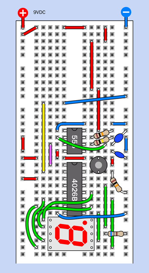
Figure 4-62. The first module of the reflex tester demonstrates how a timer can run a counter chip that powers a single-digit LED display.
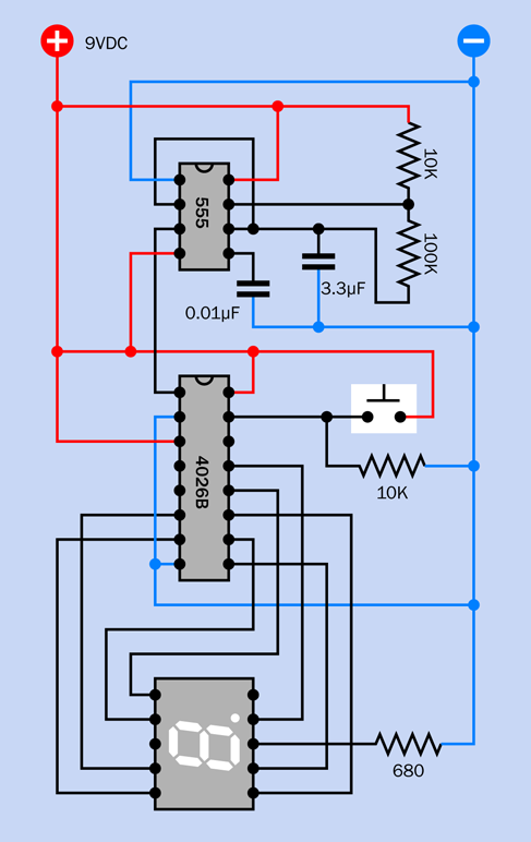
Figure 4-63. The first module shown in schematic form.
In addition, component values are shown in Figure 4-64.
You’re going to be adding a lot more components to the board (in fact, it will be packed full by the time you’re finished), so you need to position everything exactly as I have shown it in the figure. Count the rows of holes carefully! You’ll see some wires that don’t make sense right now (all those red pieces—what are they for?) but they will enable you to add and activate a couple more 555 timers as you proceed.
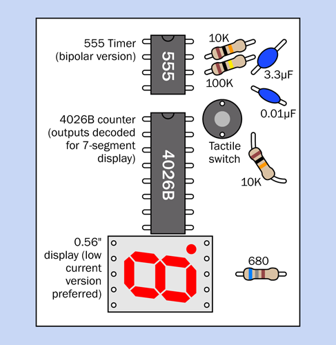
Figure 4-64. Component values for the first module of the circuit.
Apply power from a 9-volt battery or AC adapter, and you should see the numeric display counting repeatedly from 0 through 9.
If you don’t see any numerals at all, set your meter to measure DC volts, clip the black probe to the negative side of the power supply, and use the red probe to test for voltages at key locations in the circuit, such as the power input pins of the chips. If the voltages look okay, make sure the resistor at bottom-right is 680 ohms (not 68K or 680K, which are colored similarly).
If the display shows fragments of numerals, or numerals that are not counting sequentially, you made an error in the green wires connecting with the 4026B chip.
If the display shows a 0 that does not change, you wired the 555 timer wrongly, or failed to connect the timer with the 4026B chip correctly.
Once you have the numbers counting upward, hold down the tactile switch, and notice that it forces the counter back to 0. As soon as you let go of the tactile switch, the numbers start counting again.
We have the basis for a reflex tester right here. We just need to add a couple more digits, increase the counting speed, and make some more refinements. First, however, I’ll explain what’s going on.
Fundamentals: LED Displays
The term “LED” is slightly confusing. The type of component that you have used in previous experiments is properly known as a standard LED, a through-hole LED, or an LED indicator: a little rounded component with two long leads sticking out of the base. These became so common, people started calling them simply “LEDs.” But LEDs are used in other components, too, such as the glowing numeral currently plugged into your breadboard. It is properly known as an LED display. More precisely, it is a seven-segment single-digit LED display.
In Figure 4-65 the dimensions of the display are shown, along with the pin positions that are hidden underneath it. The important things to notice are that the numeral does consist of seven segments, plus a decimal point; and the pin spacings are all measured in multiples of 0.1”, which is helpful for your breadboard.
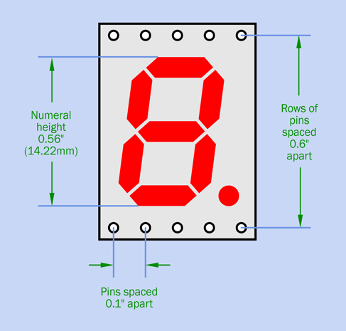
Figure 4-65. Dimensions and pin locations of a standard 0.56” seven-segment LED display.
Now take a look at Figure 4-66. This shows you the internal connections between the pins and the segments of the digit. Notice that pins 3 and 8 have blue centers, indicating that they should be connected with negative ground. All the other pins are designed to receive positive power to activate the LED segments. This is called a common cathode type of LED, because the negative sides of the internal diodes (the cathodes) are all tied together.
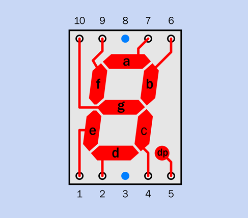
Figure 4-66. The scheme that is used for pin numbering, and the internal connections that are hidden inside the component.
In a common anode display, the situation is reversed, and you activate the segments by applying negative power to each one, while they all share a positive internal connection. You can choose whichever type of display is convenient in a circuit, but common cathode displays are more widely used.
Note that the segments are identified with lowercase letters a through g, plus dp for the decimal point. This system is common on almost all datasheets (although a few use the letter h for the decimal point).
So far so good, but I have left out a crucial piece of information: like all LEDs, the segments in the numeral must be protected with series resistors. This is a hassle, and you may wonder why the manufacturer doesn’t build resistors in. The answer is that the display must be usable on a wide variety of voltages, and the values of the resistors will depend on the voltage.
Well—why can’t we use just one resistor that all the segments share, perhaps between pin 3 and negative ground? Actually we can do that, but the resistor will be dropping the voltage and restricting the current for different numbers of segments, depending on which numeral is being displayed. A numeral 1 lights up only two segments, while a numeral 8 uses all seven of them. Consequently, some numerals will be brighter than others.
Does this really matter? I’m thinking that for this demo, simplicity may be more important than perfection. If you look at Figure 4-62 you’ll see that I have, in fact, put just one 680-ohm resistor at bottom-right, between the LED display and the negative bus. This is not the correct procedure, but you are going to install three of the seven-segment displays in this project, and I think you’ll be happy to use only three series resistors instead of 21.
Fundamentals: The Counter
The 4026B chip is known as a decade counter, because it counts in tens. Most counters have a coded output, meaning that they output the numbers in binary-coded format (which I will discuss in a later project). This counter doesn’t do things this way. It has seven output pins, and it powers them in patterns that just happen to be correct for a seven-segment display. While other counters require a driver to convert a binary output to the seven-segment patterns, the 4026B gives you everything in one package.
This is very convenient, except that the 4026B is an old-fashioned CMOS chip that has limited power. The datasheet advises you to draw less than 5mA from any one pin when powering the chip with 9 volts.
Ideally you should pass the outputs from the counter through an array of transistors, to amplify them. You can buy a chip containing seven transistor pairs for exactly this purpose. It’s called a Darlington array. (What if you want to display the decimal point? No problem. You can buy a different Darlington array containing eight transistor pairs.)
I could have used three Darlington-array chips to drive the three LED displays in this project, but that would have added to the complexity and expense, and I would have needed two breadboards. Therefore I decided it was acceptable to use low-current LED displays that can be driven directly by a counter. They’re not as bright, but they do the job. I chose the 680-ohm resistor because it should limit the current to less than 5mA from any single pin on the counter chip, and it imposes a voltage drop of around 2V across the LEDs (which varies depending how many segments are lit up).
Now I’ll give you some details about the internal workings of the 4026B. Counter chips always have several useful features built in. Take a look at Figure 4-67, which shows the pinouts of the chip. The pins with labels such as “To segment a” are easy to understand. You simply run a wire from each pin to the appropriate pin on your LED display. If you look at Figure 4-62 you’ll see each of the green wires connecting the output pins from the counter with the input pins on the numeral.
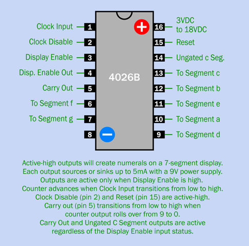
Figure 4-67. Pinouts for a 4026B counter chip, which has decoded outputs to drive a seven-segment single-digit LED display.
Pins 8 and 16 of the chip are for negative-ground and positive power, respectively. Almost all digital chips apply power to opposite corners in this way (with the exception of the 555 timer—although, really, it is classified as an analog chip).
Because Figure 4-67 contains information that you may not need and is just included for future reference, I have also created a simplified view of the counter and the display in Figure 4-68, ignoring the pins that we won’t be using, and showing the relationship of output pins with the pins on the display.
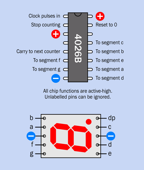
Figure 4-68. A simplified view of the chip and the display, in the style that they will be shown on the breadboard.
Look at pin 15, the reset pin. Now look at Figure 4-62. The pushbutton, more properly known as a tactile switch, is placed so that it will apply positive voltage to pin 15 when you press the button. (The voltage makes its way across the board to the pushbutton via the red segments of wire that I mentioned a moment ago.)
When you’re not pressing the button, no positive voltage is applied to the reset pin of the counter. However, a 10K resistor permanently connects pin 15 to the negative bus on the breadboard. This is a pulldown resistor. It pulls the voltage on the pin to near zero—until you press the button, at which point the positive input overwhelms the negative power supplied through the resistor. Remember, if you don’t apply a defined voltage to each input pin of a digital chip, you will get random, inexplicable, and confusing results. I’ve mentioned this before, but I have to emphasize the topic, because it’s such a common cause of errors.
-
To keep an input pin normally high, connect it to the positive bus through a 10K resistor (at least, for the circuits in this book). When you need to pull it low, use a switch or other device that overrides the resistor by making a more direct connection to the negative bus.
-
To keep an input pin normally low, connect it to the negative bus through a 10K resistor. When you need to push it high, use a switch or other device that overrides the resistor by making a more direct connection to the positive bus.
-
All the inputs on a counter chip must have some kind of connection. Never allow any floating input pins!
-
Unused output pins should be left unconnected.
One more thing. Sometimes a chip has an input that we won’t need at all. The 4026B, for instance, tells us that pin 3 is a display enable input. I want the display to be enabled all the time, so I connected pin 3 directly to the positive bus on a set-it-and-forget-it basis.
-
If you won’t be using an input pin, it must still have a defined state. You can deal with it by wiring it directly to the positive or negative side of the power supply.
Now I’ll run through the remaining features of the 4026B.
The clock input (pin 1) accepts a stream of high and low pulses. The chip doesn’t care how long the pulses are. It just responds by adding 1 to its count, each time it senses the input voltage rising from low to high.
The clock disable (pin 2) tells the counter to block the clock input. Like all the other pins on the chip, this one is active-high, meaning it performs its function when it has a high state. On your breadboard, I ran in a temporary blue wire and yellow wire to hold pin 2 low. In other words, I disabled the clock disable pin. This is confusing, so I will summarize the situation:
-
When the clock disable pin is in a high state, it stops the counter from counting.
-
When the clock disable pin is pulled down to negative ground, it allows the counter to count.
The display enable (pin 3) I already mentioned.
The display enable out (pin 4) will not be used here. It takes the state of pin 3 and connects it with pin 4 so that you can pass it along to other 4026B timers.
The carry out (pin 5) is essential if you want to count higher than 9. The pin state shifts from low to high when the counter has reached 9 and goes back to 0. If you take this output and connect it with the clock input pin of a second 4026B timer, the second timer will count in tens. You can use its carry output pin to signal a third timer, which will count in hundreds. I will be using this feature at the end of this project.
Lastly, Pin 14 can be used to restart the counter after it counts through 0, 1, and 2. This is useful in a digital clock that only counts up to 12 hours, but not relevant to us here. It is an output pin that we will not use, so it can be left unconnected.
Perhaps all the features seem confusing, but if you ever find yourself confronted with a counter chip that you’ve never seen before, you can figure it out (if you are patient and methodical) by looking up the manufacturer’s datasheet. Then you can test it with LEDs and tactile switches, to make sure there are no misunderstandings. In fact, this is how I figured out the 4026B, myself.
Pulse Generation
Because the 555 timer accepts a power supply ranging from 5 to 15 volts, just like the 4026B, the output from the timer, on pin 3, can be connected directly to the input of the 4026B. That’s the function of the purple wire in the breadboard layout. The 555 supplies pulses, and the 4026B counts them.
The rest of the wiring around the 555 timer should look familiar to you by now. You can see that it’s running in astable mode. Your only question may be why it’s running so slowly. We’re not going to measure someone’s reflexes at that speed.
True, but for this demo, I didn’t want the digits to look like a featureless blur. We’ll crank up the speed a bit later.
Time for a Plan
How should the reflex timer work? Here’s my wish list:
-
I need a start button.
-
After the start button is pressed, there is a delay in which nothing happens. Suddenly there is a visual prompt, asking the player to respond.
-
Simultaneously, the count starts from 000, in 1/1,000ths of a second.
-
The user has to press a button to stop the counting process.
-
The count freezes, showing how much time elapsed between the prompt and the stop time. This measures the user’s reflexes.
-
A reset button sets the count back to 000.
You already installed a reset button on the breadboard, which is necessary. But before that, we need a button that stops the counting process.
The counter’s clock disable pin will freeze the display, but if you want to keep the display frozen, the pin has to be held in a continuing high state. In other words, it has to be latched.
Hmmm, that sounds as if we could use another 555 timer, wired in bistable mode.
A Control System
In Figure 4-69 the bistable timer has been added, with two new buttons. The diagonal blue wire in Figure 4-62 has been removed (to make room for the new timer). The other parts that you installed previously are still there, but are shown in gray.
Figure 4-70 shows the new part of the circuit in schematic form, and values of the additional parts are shown in Figure 4-71.
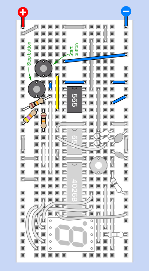
Figure 4-69. A bistable 555 timer has been added. Previously wired components are grayed out.
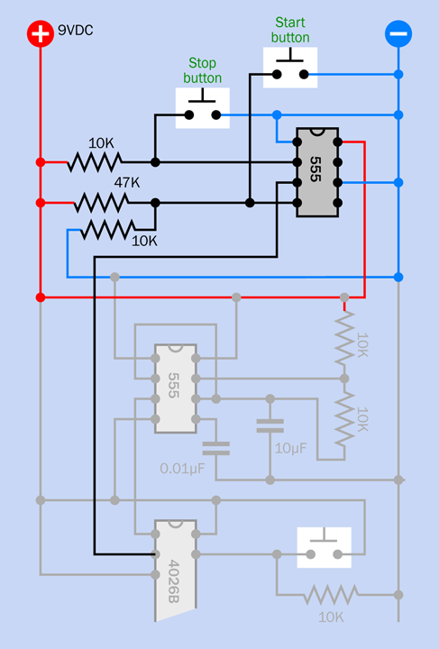
Figure 4-70. This schematic shows the second timer and its associated components. Previous components are grayed out.
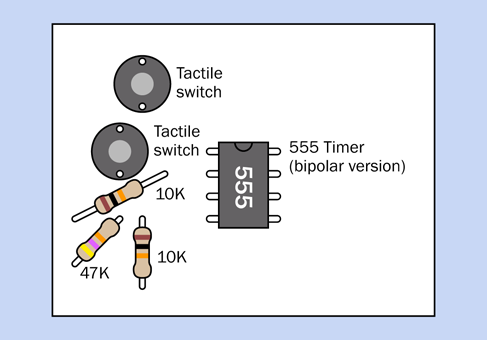
Figure 4-71. Values of the parts that have been added in this module of the project.
After you build this new section of the circuit, you can try it. You should find that the two new buttons start and stop the counting process. Do you see how they work?
Press the start button, and it grounds the reset pin of the bistable timer. The timer output on pin 3 goes low, and is connected to the clock disable pin on the counter. Remember, a low state on the disable pin means that the counter is not disabled. So, the counter starts counting. And it goes on counting, because once you trigger the bistable timer, its output is latched, and continues indefinitely.
But, you can stop it. Just press the stop button. This grounds the input pin of the bistable timer, triggering it. Consequently, the output from the timer goes high, and because the timer is working in bistable mode, the output is latched and stays high indefinitely. The high output goes to the clock disable pin, which stops the counter.
When you press the button at lower-right, which you installed initially, it still resets the timer to 000. But the timer remains latched in its disabled mode until you restart it with the start button.
The bistable 555 was exactly what we needed to run this circuit.
Progress Report
Let’s see how far we’ve proceeded in satisfying the wish-list. It looks to me as if we’re almost there. You press a button to start it, press a second button to stop it, and then once it’s stopped, you press another button to set it to zero.
The only thing missing is the element of surprise. Really the person using it shouldn’t know when the count will start. The idea is to measure the speed of his reflexes when he responds.
Why not add yet another timer, in monostable mode, to insert a delay before the action begins? This way, the start will be unexpected.
The Delay
First remove the start button, and the diagonal piece of blue wire connecting it with the negative bus. Leave the vertical yellow piece of wire where it is.
Now assemble some additional components as shown in Figure 4-72. The start button has been relocated to trigger the input of a third timer, which will insert a preliminary delay. The output from this timer will go high for 5 or 10 seconds, and then when it goes low it triggers the bistable timer, sending its output low, to suppress the clock disable feature of the 4026B, so that it starts counting.
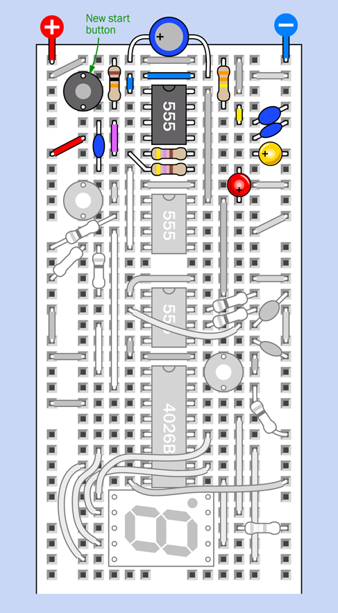
Figure 4-72. The upper part of the reflex timer circuit is now complete.
Be careful when installing the red and yellow LEDs. The red one is the opposite way around from what you might expect, because it is tied in to a positive source. So, its long, positive lead is at the bottom, not the top.
A schematic version of the new part of the circuit appears in Figure 4-73.
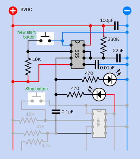
Figure 4-73. Schematic for the new and final addition to the control circuit.
The values of the parts that you added to the breadboard are shown in Figure 4-74.
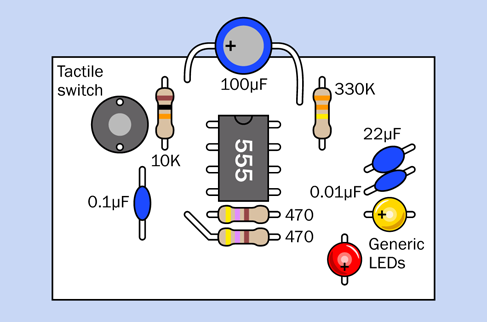
Figure 4-74. The values of parts that have been added to the breadboard.
Testing
When you apply power to this circuit, the counter immediately starts counting, without you asking it to. This is annoying, but easily dealt with. Press the stop button to stop the count. Press the bottom-right pushbutton to reset the timer to zero. Now you’re ready for action.
Press the new start button, which creates an initial delay. During this delay, the yellow LED lights up. The delay lasts for about seven seconds, at which point the yellow LED goes out and the red LED comes on. Simultaneously, the counter starts counting—until you press the stop button.
The 100µF capacitor at the top of the breadboard looks like an afterthought, but is actually quite important. The 555 timer has a bad habit of creating voltage spikes when it switches its output, and in this circuit, the spikes can trigger the second timer without waiting for the delay. The 100µF capacitor suppresses this unfortunate tendency.
We now have all the features installed, except for the need to increase the counter speed and add a couple more counters and displays for fractions of a second.
How Does It Work?
Figure 4-75 shows you how the components are communicating with each other.
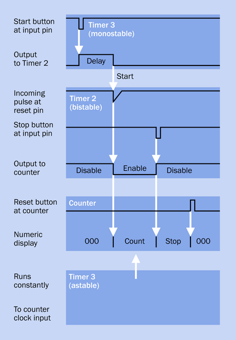
Figure 4-75. Interaction between the components in the timer control circuit.
I’ll describe this figure from top to bottom. The start button (at the top, connected with Timer 3) pulls the input of the timer low to trigger it.
The output of Timer 3 goes high for about seven seconds. This creates your initial delay.
At the end of the delay, the output from Timer 3 drops back down. This transition passes through a 0.1µF coupling capacitor to Timer 2, which is bistable. The capacitor allows only a brief pulse to reach the reset pin of Timer 2. The pulse sends the output of Timer 2 low. This low output goes to the clock disable pin of the 4026B counter. A low state enables the counter, and the count begins.
Now we wait for the user to respond. The user presses the stop button for Timer 2, connected with its input on pin 2. The brief low input to Timer 2 sends its output high, which enables the clock disable pin on the counter, and stops the count.
Background: Development Issues
This project created a problem. When I built the original circuit several years ago, it ran fine. When some interns at Make: magazine built the circuit, it ran fine. Little did we know that the reset pin of a 555 timer behaves slightly differently on different brands. This is not documented on the datasheet.
After my book had been in print for literally years, I received notification from a reader that his version of the circuit functioned erratically, and sometimes not at all. I rebuilt the circuit, connected it with an oscilloscope, and saw that the coupling capacitor was transmitting a pulse faithfully from Timer 3 to the reset pin of Timer 2. But, sure enough, Timer 2 sometimes didn’t recognize the pulse.
What was the problem? Either the pulse was too brief, or it didn’t go low enough. Either way, the solution was to apply a lower pullup voltage to pin 4 of Timer 2. This is why you see two resistors attached to pin 4. They function as a voltage divider, applying slightly less than 2V to pin 4. This is enough to keep it functional, but allows the reset voltage to go down lower to enable the reset.
This now works fine—for me. We’ll test the circuit again before this edition of the book goes into print. If it doesn’t work for you, try applying a different voltage to pin 4 of Timer 2, using a substitute for the 47K resistor, either lower or higher. You can also try a larger coupling capacitor. And let me know. Obviously I want all the circuits in this book to work properly, every time. But I can’t foresee all the manufacturing variations that may affect the outcome.
Extra Digits
Adding two more digits is pretty easy, as each will be controlled by its own 4026B counter, and all the counters and digits will be wired in basically the same way. This is shown in Figure 4-76.
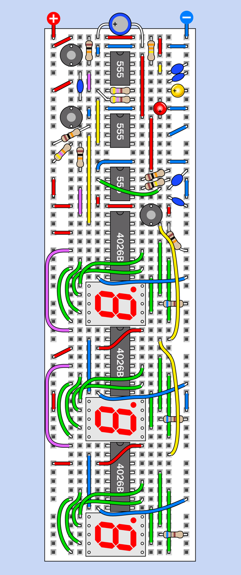
Figure 4-76. The completed reflex timer barely fits on one 60-row breadboard.
Notice the purple wires on the left. Each of them connects the carry output from one counter to the clock input of the next.
The yellow wires down the right side connect all the reset inputs of the counters together, so that when you reset one, you reset them all.
In the second and third counters, blue wires have been added to ground pin 2 of each. Remember, pin 2 is the clock disable pin. We never need to stop the second and third counters from counting, because they are completely under the control of the first counter. When it stops, they stop.
Don’t forget to supply positive voltage to pin 16 (the power input pin) of the second counter and the third counter, by running a red wire across each chip, as shown.
Calibration
How do you make the circuit run at the right speed?
Begin by substituting a 10K resistor for the 100K resistor on the first timer that you installed, and replace the 3.3µF capacitor with a 47nF capacitor (0.047µF). In theory this should create a timer frequency of 1,023Hz, which is very close to the 1,000Hz that you want.
To fine-tune it, you’ll have to substitute a trimmer potentiometer for one of the 10K resistors on the first timer that you installed. This circuit is so densely packed, there’s barely enough room, but I figured out a way to squeeze in a trimmer. This is shown in Figure 4-77, which is a close-up of the immediate area around the lowest of the three timers.
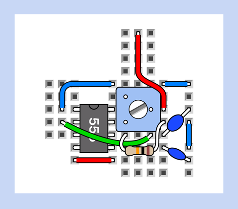
Figure 4-77. How to squeeze in a trimmer to enable adjustment of your reflex tester.
First move the blue wires up by one row. Snake the vertical red wire around the righthand side. Extend the lead from the remaining 10K resistor, taking care not to allow it to touch any other exposed conductors. You can now insert a trimmer, with its wiper pin making contact with the positive supply and another pin connecting with pin 7 of the timer. The third trimmer pin plugs into a vacant row on the breadboard, and can be ignored.
You should use a trimmer rated at 20K or 25K and start with it around the middle of its range. You now have three options to fine-tune the circuit so that it runs at 1kHz.
If you happen to have a multimeter with a setting on its dial to measure kHz, simply ground the black meter probe, touch the red probe to pin 3 of the first timer that you installed, and turn the trimmer until the meter shows 1kHz. Job done!
If you don’t have a meter than measures frequency, perhaps you have a digital guitar tuner. They only cost a few dollars on eBay. Attach a loudspeaker to the output from the 555 timer (including a 10µF coupling capacitor and a 47-ohm series resistor), and the tuner should tell you the frequency of the note being generated by the timer.
If you don’t have a suitable meter or guitar tuner, you can use any watch, clock, or phone that will display whole seconds. When the timer is running at 1kHz, the second counter will advance every 1/100th of a second, and the third counter will advance every 1/10th of a second. The third counter goes through 10 digits before repeating, which means it will display a zero once each second.
The problem is, each digit is illuminated so briefly, you’ll have a hard time seeing precisely when the zero comes up. So here’s what you do.
Cover all the segments of the slowest display except the segment at its bottom-right corner. This is illuminated all the time except when a 2 is displayed, at which point it blinks off. You’ll have a much easier time counting the blinks of this single segment than if you try to recognize whole numbers. Adjust the trimmer potentiometer that you added, and gradually you should be able to synchronize the slowest display with a timekeeping device.
Enhancements
Whenever I finish a project, I see opportunities to improve it. Here are some ideas:
No counting at power-up. It would be nice if the circuit begins in its “ready” state, rather than already counting. I’m going to leave you to think about this.
Audible feedback when the red LED lights up. Not essential, but might be a nice feature.
A random delay interval before the count begins. Making electronic components behave randomly is very difficult, but one way to do it would be to require the user to hold his finger on a couple of metal contacts. The skin resistance of the finger would determine the delay. Because the finger pressure would not be exactly the same each time, the delay would vary.
Next?
A counter such as the 4026B is technically a logic chip. It contains logic gates that enable it to count. Every digital computer works on similar principles.
Because logic is so fundamental in electronics, I’m going to delve into it at much greater depth, beginning with the next experiment. The magic words AND, OR, NAND, NOR, XOR, and XNOR will open a whole new world of digital intrigue.
Experiment 20: Learning Logic
When you deal with logic gates individually, they’re extremely easy to understand. When you chain them together, they become more challenging. So I’ll start with them one at a time.
This experiment contains a significant amount of explanation. I don’t expect you to remember it all. The purpose here is to provide a store of information that you can refer back to, later.
What You Will Need
-
Breadboard, hookup wire, wire cutters, wire strippers, test leads, multimeter
-
9-volt power supply (battery or AC adapter)
-
SPDT slide switch (1)
-
74HC00 quad 2-input NAND chip (1)
-
74HC08 quad 2-input AND chip (1)
-
Low-current LEDs (2)
-
Tactile switches (2)
-
LM7805 voltage regulator (1)
-
Resistors: 680 ohms (1), 2.2K (1), 10K (2)
-
Capacitors: 0.1µF (1), 0.33µF (1)
The Regulator
Logic gates are much fussier than the 555 timer or the 4026B counter that you used previously. The versions that we will be using demand a precise 5VDC, with no fluctuations or “spikes” in the flow of current.
This is easy and inexpensive to achieve. Just set up your breadboard with an LM7805 voltage regulator. It delivers a well-controlled voltage of 5 volts if you supply it with a DC voltage of 7 volts or more.
For a diagram of the regulator showing its three pin functions, see Figure 4-78. For a schematic showing how to use the regulator, see Figure 4-79. For a suggestion of how to place the regulator and its two capacitors at the top of a breadboard, to occupy minimum space, see Figure 4-80. I have added a miniature on-off slide switch at top-left, and a low-current LED to show when power is connected. I think a visual indicator is useful to provide assurance that the power is on, especially when you’re searching for a fault in a circuit. The high-value 2.2K resistor for the LED is chosen to consume as little current as possible, in case you are still using a 9-volt battery as your power supply.
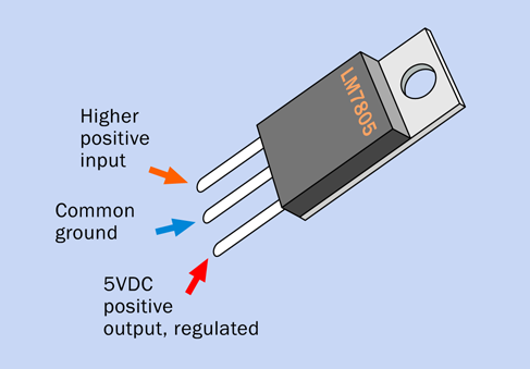
Figure 4-78. Pin functions of the LM7805 voltage regulator, shown with the metal back facing away from you.
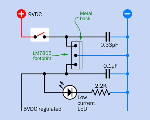
Figure 4-79. How to use the LM7805 voltage regulator. The capacitors are mandatory.
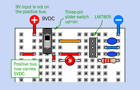
Figure 4-80. Placing a voltage regulator at the top of a breadboard, to occupy minimal room while also allowing for an on-off slide switch and a low-current LED to show that power is switched on.
Caution: Inappropriate Inputs
DC, not AC. Remember that the LM7805 is a DC-to-DC converter. Do not confuse it with an AC adapter, which uses alternating current from an outlet in your home, and converts it to DC. Do not apply AC to the input of your voltage regulator.
Maximum Current. The LM7805 does a wonderful job of maintaining its output at an almost constant voltage, regardless of how much current you draw through it—so long as you stay within its rated range. Don’t try to pull more than one amp through the voltage regulator.
Maximum Voltage. Although the voltage regulator is a solid-state device, it behaves a little like a resistor in that it radiates heat in the process of reducing a voltage. The higher the voltage you put into the regulator, and the more current that passes through it, the more heat it must get rid of. Theoretically you could use an input of 24VDC and still get a regulated output of 5VDC, but this would not be a good idea. A good input range would be 7VDC to 12VDC.
Minimum Voltage. Like all semiconductor devices, the regulator delivers a voltage that is lower than its input voltage. This is why I suggest a minimum input of 7VDC.
Heat Sinking. The purpose of the metal back with a hole in the top is to radiate heat, which it will do more effectively if you bolt it to a piece of aluminum, since aluminum conducts heat very effectively. The aluminum functions as a heat sink, and you can buy fancy ones that have multiple cooling fins. If you’re not planning to draw more than 200mA through the regulator, a heat sink is unnecessary. The circuits in this book will require less than that.
Usage
When building circuits using 5-volt logic chips, you want 5VDC to be available down the positive bus of your breadboard. Note very carefully that the 9-volt input to the circuit in Figure 4-80 is not on the positive bus, but is applied only to the upper pin on the voltage regulator. The 5VDC output from the lower pin of the voltage regulator is connected with the positive bus.
The negative bus on the breadboard is shared by the voltage regulator and your external voltage supply. This is known as a “common ground.”
After you install your voltage regulator, set your meter to measure DC volts and measure the voltage between the two buses on the breadboard, just to make sure. Logic chips will be easily damaged by incorrect or reversed voltage.
Your First Logic Gate
Now that you have your 5VDC breadboard ready, take a couple of tactile switches, two 10K resistors, a low-current LED, and a 680-ohm resistor, and set them around a 74HC00 logic chip as shown in Figure 4-81. (Because you are using a low-current LED, a 680-ohm resistor is appropriate.)
You may notice that many of the pins of the chip are shorted together and connected to the negative side of the power supply. I’ll explain that in a moment.
When you connect power, the LED should light up. Press one of the tactile switches, and the LED remains illuminated. Press the other tactile switch, and again the LED stays on. Now press both switches, and the light should go out.
Pins 1 and 2 are logic inputs for the 74HC00 chip. By default, the circuit holds them at a low voltage, being connected to the negative side of the power supply through 10K pulldown resistors. But each pushbutton overrides its resistor and forces the input pin to rise near to the value of the 5V positive bus.
-
When an input or output associated with a 5V logic chip is near 0VDC, we say it is logic-low.
-
When an input or output associated with a 5V logic chip is near 5VDC, we say it is logic-high.
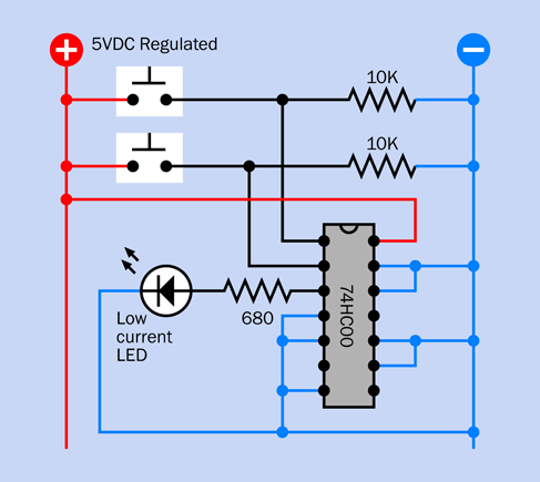
Figure 4-81. Figuring out the logical function of the NAND gate.
The logic output from the chip, as you saw, is normally high—but not if the first input and the second input are high. Because the chip does a “Not AND” operation, we say that it contains a NAND logic gate.
Logic gates can be represented with special symbols that are used in a kind of schematic known as a logic diagram. The logic diagram that corresponds with the circuit in Figure 4-81 is shown in Figure 4-82, where the U-shaped thing with a circle at the bottom is the logic symbol for a NAND gate. No power supply is shown for it in a logic diagram, but if you refer back to the schematic in Figure 4-81, the chip does in fact require power, at pins 7 (negative ground) and 14 (positive). This enables the chip to put out more current than its inputs take in.
-
Any time you see a symbol for a logic chip, remember that it needs power to function.
The 74HC00 chip actually contains four separate NAND gates, each of which has two logical inputs and one output. They are arrayed as shown in Figure 4-83, in the diagram on the right. Because only one gate was needed for the simple test, the input pins of the unused gates were shorted to the negative side of the power supply, to stop them from floating.
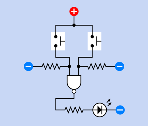
Figure 4-82. A logic diagram can be easier to understand than a schematic showing a logic chip.
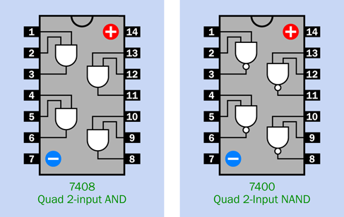
Figure 4-83. The arrangement of gates inside two logic chips.
Many logic chips are interchangable. In fact, let’s try that right now. First, disconnect the power. Carefully pull out the 74HC00 and put it away with its legs embedded in conductive foam (or aluminum foil, if you don’t have any foam). Substitute a 74HC08 chip, which is an AND chip. Make sure you have it the right way up, with its notch at the top. Reconnect the power and use the pushbuttons as you did before. This time, you should find that the LED comes on if the first input AND the second input are both positive, but it remains dark otherwise. Thus, the AND chip functions exactly opposite to the NAND chip. Its pinouts are shown in Figure 4-83, on the left.
You may be wondering why these things are useful. Soon you’ll see that we can put logic gates together to do things such as create an electronic combination lock, or a pair of electronic dice, or a computerized version of a TV quiz show where users compete to answer a question. If you were insanely ambitious, you could build an entire computer out of logic gates. A hobbyist named Bill Buzbee actually built a web server from vintage logic chips—see Figure 4-84.
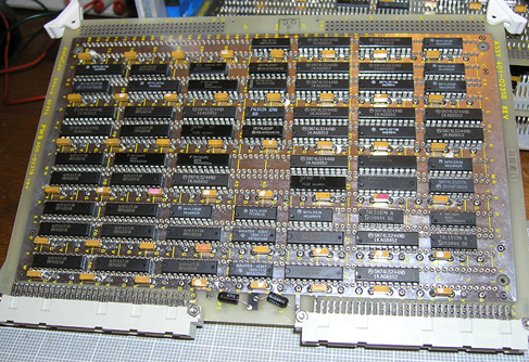
Figure 4-84. This computer motherboard hand-made by Bill Buzbee is built from 74xx series logic chips, and functions as the hearts of a web server.
Background: Logical Origins
George Boole was a British mathematician, born in 1815, who did something that few people are ever lucky enough or smart enough to do: he invented an entirely new branch of mathematics.
Interestingly, it was not based on numbers. Boole had a relentlessly logical mind, and he wanted to reduce the world to a series of true-or-false statements that could overlap in interesting ways.
Venn diagrams, conceived around 1880 by a man named John Venn, can be used to illustrate some logical relationships of this type. Figure 4-85 shows the simplest possible Venn diagram, where I have established one very large group (all the creatures in the world) and have defined a subgroup (consisting only of those creatures that live in the water). The Venn diagram illustrates that all creatures that live in water also live in the world, but only a subset of creatures in the world live in the water.

Figure 4-85. The simplest possible relationship between a group and the larger world that contains it.
Now I’ll introduce another group: creatures that live on land. But wait—some creatures are able to live on both land and water. Frogs, for instance. These amphibians are members of both groups, and I can show this with another Venn diagram in Figure 4-86, where the groups overlap.

Figure 4-86. This Venn diagram is a way of showing that some creatures in the world live on land, some live in water, and some inhabit both land and water.
However, not all groups overlap. In Figure 4-87 I have created one group of creatures with hooves, and another group of creatures with claws. Are there any creatures that have hooves and claws? I don’t think so. I could express this by creating a truth table, as in Figure 4-88.

Figure 4-87. Some subgroups do not overlap. I don’t think any creatures have claws as well as hooves.

Figure 4-88. The simplest form of a truth table tabulates the validity of pairs of inputs, each of which can have one of two states.
A NAND gate could be used to represent this table, because its pattern of inputs and outputs is exactly the same, as shown in Figure 4-89.

Figure 4-89. This truth table for a NAND gate has exactly the same pattern as the previous table.
Beginning with these very simple concepts, Boole developed his logic language to a very high level. He published a treatise on it in 1854, long before it could be applied to electrical or electronic devices. In fact, during his lifetime, his work seemed to have no practical applications at all. But a man named Claude Shannon encountered Boolean logic while studying at MIT in the 1930s, and in 1938 he published a paper describing how Boolean analysis could be applied to circuits using relays. This had immediate practical applications, as telephone networks were growing rapidly, creating complicated switching problems.
A very simple telephone problem could be expressed like this. Long ago, it was common for two customers living in separate homes in a rural area to share one telephone line. If one of them wanted to use the line, or the other wanted to use it, or neither of them wanted to use it, there was no problem. But they could not both use it simultaneously. Once again, this is the same logical pattern as described in Figure 4-89, if we interpret “high” to mean that one person wants to use the line, and “low” meaning that the person doesn’t want to use it.
But now there’s an important difference. The NAND gate doesn’t just illustrate the network. Because the telephone network uses electrical states, a NAND gate can control the network. (Actually, in the early days of networks, everything was done by relays; but an assembly of relays can still function as a logic gate.)
After Shannon’s application of Boolean logic to the telephone system, the next step was to see that if you used an “on” condition to represent numeral 1 and an “off” condition to represent numeral 0, you could build a system of logic gates that could count. And if it could count, it could do arithmetic.
When vacuum tubes were substituted for relays, the first practical digital computers were built. Then transistors took the place of vacuum tubes, and integrated circuit chips replaced transistors, leading to the desktop computers that we now take for granted. But deep down, at the lowest levels of these incredibly complex devices, they still use the laws of logic discovered by George Boole.
Incidentally, when you use a search engine online, if you use the words AND and OR to refine your search, you’re actually using Boolean operators.
Fundamentals: Logic Gate Basics
The NAND gate is the most fundamental building block of digital computers, because you can do addition sums using nothing but NANDs. If you want to learn more about this, search online for topics such as “binary arithmetic” and “half-adder.” You can also find circuits that do addition sums using logical operators in my book Make: More Electronics.
Generally, there are seven types of logic gates:
AND, NAND, OR, NOR, XOR, XNOR, NOT
Their names are usually printed entirely in capital letters. Of the first six, XNOR is hardly ever used.
All of the gates have two inputs and one output, except for the NOT gate, which has only one input and one output, and is more often referred to as an inverter. If it has a high input, it gives a low output, and if it has a low input, it gives a high output.
Symbols that represent the seven types of gates are shown in Figure 4-90. Notice that the little circles at the bottom of some of the gates invert the output. (These circles are called bubbles.) Thus, the output of a NAND gate is the inverse of an AND gate.

Figure 4-90. Symbols for the six two-input logic gates, plus the NOT gate.
What do I mean by “inverse”? This should become clear if you look at the truth tables for logic gates that I have drawn in Figure 4-91, Figure 4-92, and Figure 4-93. In each of the tables, two inputs are shown on the left followed by an output on the right, with red meaning a high-logic state and blue meaning a low-logic state. Compare the outputs of each pair of gates, and you’ll see how the patterns are inverted.

Figure 4-91. The inputs shown on the left produce the outputs shown on the right.
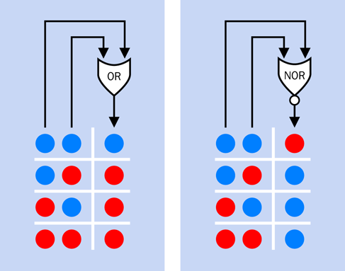
Figure 4-92. The inputs shown on the left produce the outputs shown on the right.

Figure 4-93. The inputs shown on the left produce the outputs shown on the right.
Background: The Confusing World of TTL and CMOS
Back in the 1960s, the first logic gates were built with transistor–transistor logic, abbreviated TTL, meaning that tiny bipolar transistors were etched into a single wafer of silicon. Soon, these were followed by complementary metal oxide semiconductors, abbreviated CMOS. The 4026B chip that you used in Experiment 19 is an old CMOS chip.
You may remember that bipolar transistors amplify current. Thus, TTL circuits require a significant flow of electricity to function. But CMOS chips are voltage-sensitive, enabling them to draw hardly any current while they are waiting for a signal, or while they are pausing after emitting a signal.
The table in Figure 4-94 summarizes the original advantages and disadvantages of the two types of chips. The CMOS series, with part numbers from 4000 upward, were slower and more easily damaged by static electricity, but were valuable because of their meager power consumption. The TTL series, with part numbers from 7400 upward, used much more power but were less sensitive and very fast. So, if you wanted to build a computer, you used the TTL family, but if you wanted to build a little gizmo that would run for weeks on a small battery, you used the CMOS family.

Figure 4-94. In this table comparing early CMOS and TTL chips, the CMOS attributes with a question mark were eventually reconciled with the TTL attributes.
From this point on everything became confusing, because CMOS manufacturers wanted to grab market share by emulating the advantages of TTL chips. Newer generations of CMOS chips even changed their part numbers to begin with “74” to emphasize their compatibility, and the functions of pins on CMOS chips were swapped around to match the functions of pins on TTL chips. The voltage requirements of CMOS were also changed to match TTL.
Today, you can still find some of the old TTL chips around, especially in the LS series (with part numbers such as 74LS00 and 74LS08). However, they have become uncommon.
It’s more common to find the 4000 series CMOS chips—such as the 4026B that you used in the previous experiment. They are still being made because their wide range of acceptable power-supply voltages is useful.
Over the years, CMOS chips became faster and less vulnerable to static electricity, which explains why I added a question mark in these categories in Figure 4-94. Modern CMOS chips also mostly reduced their maximum power supply voltages to 5VDC—which is why I added a question mark in this category, too.
The situation can be summed up like this:
-
Any logic chips still available in the old 4000 series will have the features I have listed in Figure 4-94. You are quite likely to find a use for the 4000 series of chips.
-
You are unlikely to use old TTL chips in the 7400 series, because they have no significant advantages.
You may still find schematics that specify 74LSxx chips. You can substitute the 74HCTxx chips, which are designed to function identically.
The 74HCxx generation is by far the most popular in through-hole format. They have the high input impedance of CMOS, which is useful, and they are cheaper than some of the more modern, exotic versions. All of the logic chips in this book are of the HC type.
Now for the part numbering. Where you see a letter “x” in the list that follows, it means that various letters and numbers may appear in that location. Thus “74xx” includes the 7400 NAND gate, the 7402 NOR gate, the 74150 16-bit data selector, and so on. A combination of letters preceding the “74” identifies the chip manufacturer, while letters following the part number may identify the style of package, may indicate whether it contains heavy metals that are environmentally toxic, and other details. This is explained visually in Figure 4-3.
Here’s the history of the TTL family:
-
74xx: The old original generation, now obsolete.
-
74Sxx: Higher speed “Schottky” series, now obsolete.
-
74LSxx: Lower power Schottky series, still used occasionally.
The CMOS family:
-
40xx: The old original generation, now obsolete.
-
40xxB: The 4000B series was improved but still susceptible to damage from static electricity. These chips are still commonly used, especially in hobby-electronics applications.
-
74HCxx: Higher-speed CMOS, with part numbers matching the TTL family, and pinouts matching the TTL family. I’ve used this generation extensively in this book, because it’s widely available, and the circuits here have no need for greater speed or power.
-
74HCTxx: Like the HC series but matching the old TTL standard for maximum and minimum logic-low and logic-high voltages, respectively.
-
74xx series with other letters in the middle of the part number: More modern, faster, usually surface-mount, often designed for lower operating voltages.
What You Don’t Need
Speed differences are irrelevant from our point of view, as we’re not going to be building circuits running at millions of cycles per second.
Price differences between chip families are usually minor when purchased in low quantities.
Lower-voltage chips are not appropriate for our purposes, as they are almost all surface-mount format, and we would have to create a lower-voltage power supply. Because surface-mount chips are so much more difficult to deal with, and their only major advantage is miniaturization, I won’t be using them. Through-hole equivalents have the same logic functions.
Fundamentals: Part Numbers and Functions
The interior connections of currently available through-hole 14-pin logic chips in the HC series are shown in Figure 4-83, Figure 4-95, Figure 4-96, Figure 4-97, Figure 4-98, Figure 4-99, Figure 4-100, and Figure 4-101.
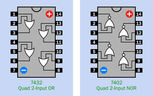
Figure 4-95. Standardized configuration of gates in the 74xx family of logic chips.
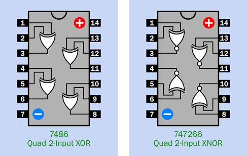
Figure 4-96. Standardized configuration of gates in the 74xx family of logic chips.
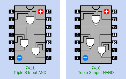
Figure 4-97. Standardized configuration of gates in the 74xx family of logic chips.
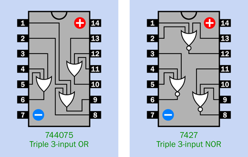
Figure 4-98. Standardized configuration of gates in the 74xx family of logic chips.
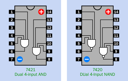
Figure 4-99. Standardized configuration of gates in the 74xx family of logic chips.
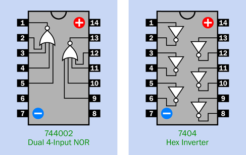
Figure 4-100. Standardized configuration of gates in the 74xx family of logic chips.
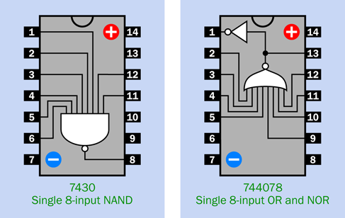
Figure 4-101. Standardized configuration of gates in the 74xx family of logic chips.
All the part numbers in these chips are shown in their minimal form. Thus the 7400 chip may have actual part numbers such as 74HC00, 74HCT00, and so on, and will be preceded and followed by other letter codes; but it is generically referred to as a 7400 chip, so that’s how I present it here.
It’s very important to check the pin functions of logic chips against the diagrams here or a manufacturer’s datasheet before using them. Interior connections may seem to follow similar patterns, but there are exceptions.
Fundamentals: Rules for Connecting Logic Gates
Permitted:
-
You can connect the input of a gate directly to your regulated power supply, either positive side or negative side.
-
You can connect the output from one gate directly to the input of another gate.
-
The output from one gate can power the inputs of many other gates (this is known as “fanout”). The exact ratio depends on the chip, but in the 74HCxx series, you can always power at least ten inputs with one logic output.
-
The output from a logic chip can drive the trigger (pin 2) of a 555 timer, so long as the timer shares the same 5VDC power supply.
-
Low input doesn’t have to be zero. A 74HCxx logic gate will recognize any voltage up to 1 volt as “low.”
-
High input doesn’t have to be 5 volts. A 74HCxx logic gate will recognize any voltage above 3.5 volts as “high.”
The acceptable ranges for inputs, and the minimum guarantees for outputs, are shown in Figure 4-102.

Figure 4-102. To avoid errors, stay within the recommended input ranges for logic chips.
Not permitted:
-
No floating inputs! On CMOS chips, such as the HC family, you must always connect all input pins with a known voltage. This includes the input pins of gates that are unused on a chip.
-
Any single-throw switch or pushbutton should be used with a pullup or pulldown resistor, so that when the contacts are open, the input to the chip is not floating.
-
Don’t use an unregulated power supply, or more than 5 volts, or less than 5 volts, to power 74HCxx logic gates.
-
Be careful when using the output from a 74HCxx logic chip to power an LED. You can draw as much as 20mA from the chip, but this will pull down the output voltage. If you are also connecting that voltage to the input of a second chip, the voltage may be pulled down so much by the LED that the second chip doesn’t recognize it as “high” anymore. Generally, try not to use a logic output to power an LED at the same time as another logic chip. Always check currents and voltages when modifying a circuit or designing a new one.
-
Throughout this book, I am using low-current LEDs in conjunction with logic-chip outputs, because I think this is a good habit to acquire, in case an output powering an LED is also used as a logic input for another chip at some point in the future.
-
Never apply a significant voltage or current to the output pin of a logic gate. In other words, don’t force an output into another output.
-
For this reason, don’t tie the outputs together from two or more logic gates.
So much for the dos and don’ts. Now it’s time for your first real logic-chip project.
Experiment 21: A Powerful Combination
Suppose you want to prevent other people from using your computer. I can think of two ways to do this: using software, or using hardware. The software would be some kind of startup program that intercepts the normal boot sequence and requests a password. It would be a little more secure than the password protection that is a standard feature of Windows and Mac operating systems.
You could certainly do it that way, but I think it would be more fun (and more relevant to this book) to do it with hardware. What I’m imagining is a numeric keypad requiring the user to enter a secret combination before the computer can be switched on. I’ll call it a “combination lock,” even though it won’t actually lock anything. It will disable the power-on button that you normally use to switch on your computer.
Caution: The Warranty Issue
If you follow this project all the way to its conclusion, you’ll open your desktop computer, cut a wire, and insert your own little circuit. You won’t be going near any of the boards inside the computer, and you will only access the wire to the computer’s “power on” button, but still, if you bought your computer new, you will void your warranty. I don’t take this too seriously, myself, but if that makes you uneasy, here are three options:
-
Breadboard the circuit for fun, and leave it at that.
-
Use the circuit on some other device.
-
Use it on an old computer.
What You Will Need
-
Breadboard, hookup wire, wire cutters, wire strippers, multimeter
-
9-volt power supply (battery or AC adapter)
-
Low-current LED (1)
-
Generic LED (1)
-
LM7805 voltage regulator (1)
-
74HC08 logic chip (1)
-
555 timer chip (1)
-
2N2222 transistor (1)
-
DPDT 9VDC relay (1)
-
Diodes: 1N4001 (1), 1N4148 (3)
-
Resistors: 330 ohms (1), 470 ohms (1), 1K (1), 2.2K (1), 10K (6), 1M (1)
-
Capacitors: 0.01µF (1), 0.1µF (1), 0.33µF (1), 10µF (2)
-
Tactile switches (8)
-
Optional: Tools to open your computer, drill four holes, and make saw cuts between the holes, to create a rectangular opening for the keypad (if you want to take this project to its conclusion). Also, four small bolts to attach the keypad to the computer cabinet after you create the opening for it
A Three-Part Circuit
The entire breadboarded circuit is shown in Figure 4-107, but before you start to build it, let’s take a look at the schematics.
The circuit is divided into three sections:
-
Power supply and three dummy pushbuttons.
-
Active pushbuttons and logic.
-
Output.
The schematic in Figure 4-103 shows part 1. This is simple enough. When you press button A, this supplies 9VDC to the voltage regulator, which delivers 5VDC down the lefthand bus. The button also supplies 9VDC down a magenta-colored wire on the right, for reasons which I’ll get to in a moment.
In addition you will notice buttons B, C, and D, any one of which makes a connection with negative ground.
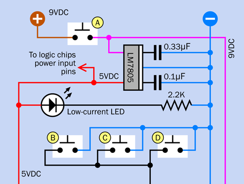
Figure 4-103. The top section of the circuit.
Now take a look at Figure 4-104, which shows the center section of the circuit using logic symbols. Imagine this attached to the top part of the circuit in Figure 4-103. Each of the buttons E through H can supply positive voltage to an AND gate, whose lefthand input is normally held low through a 10K pulldown resistor. The output from each gate feeds an input of the next gate.
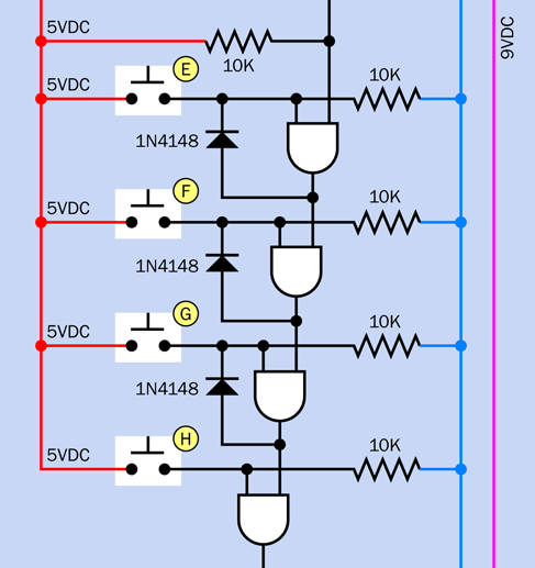
Figure 4-104. The middle section of the circuit, using logic symbols.
Lastly, Figure 4-105 shows the bottom section of the circuit, where the output from the last of the AND gates activates a transistor, which triggers a 555 timer. The timer controls a relay, and the relay will be used to lock and unlock your computer (or any other device that uses a simple on-off button).
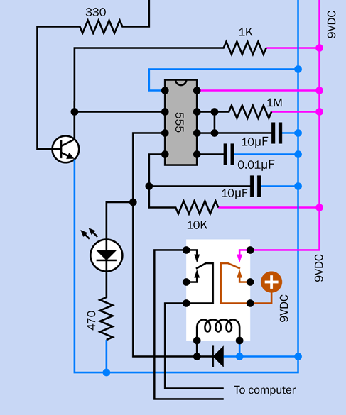
Figure 4-105. The bottom section of the circuit.
How It Works
I have set this up so that you have to hold down button A to activate the circuit, and you have to continue pressing it while you enter a secret sequence on the pushbuttons. This satisfies two purposes: the circuit draws no power while you’re not using it, and you can’t leave it switched on by mistake.
The secret sequence consists of pressing buttons E, F, G, and H in that order, while you are holding down button A. Of course if you actually install the circuit, you can scramble the positions of the buttons. I laid them out like this on the breadboard for the sake of simplicity.
Suppose you are holding down button A, and you press button E as the first in the sequence to unlock the circuit. In Figure 4-104 you can see that button E conducts 5 volts directly to the left input of the first AND gate. This overcomes the pulldown resistor, so the left input is now logic-high.
The righthand input of the AND gate is being held high through a 10K resistor. So, now both inputs of the AND gate are high, and consequently its output changes from low to high.
Current from the output circulates around through a diode, to the lefthand input. Consequently, you can let go of button E, and the output from the AND gate will maintain the lefthand input in a high state. The gate has latched itself, like the relay in Experiment 15. It is able to do this because it has its own power supply (not shown in the logic schematic) which sustains the output voltage regardless of small reductions in the input voltage.
The high output from the first AND gate also connects with the righthand input of the second AND gate. Now that the second AND gate has a high righthand input, if you press the button to pull up the lefthand input, the output from the second AND gate goes high. Note that the button wouldn’t have worked before, because you needed a high output from the first AND gate to feed the second AND gate.
-
After you press each button, the AND gate beside it latches itself, and you can release the button.
-
You have to press the buttons in sequence. If you press four buttons out of sequence, nothing happens.
-
You have to hold down button A throughout the whole procedure.
Now take a look at buttons C, D, and E. What happens if you press any of these buttons while you are entering the code to unlock the circuit? Any of the buttons will pull down the voltage on the righthand input of the first AND gate. Consequently, the output from the AND gate will go low. If the gate had latched itself, it comes unlatched. Moreover, the low output from the first AND gate will unlatch the second AND gate, and the low output from the second AND gate will unlatch the third AND gate.
Any of buttons C, D, and E will reset the whole circuit. I included them just to make entering the correct combination more difficult. Naturally I am assuming that if you install this system, all the buttons will look the same.
More than One Button?
What if someone presses more than one button simultaneously (while holding down button A)? The results will be unpredictable. If all the buttons E, F, G, and H are pressed together, the relay will be activated—except that if any of the buttons B, C, or D is also pressed, this will stop anything from happening. The possibility of simultaneous button presses can be seen as a flaw in this circuit, but the chance of someone pressing A, E, F, G, and H while not pressing B, C, or D is small. To reduce this risk further, you could add more “reset” buttons in parallel with B, C, and D.
Triggering the Relay
Suppose you enter the correct combination. The last AND gate applies about 5 volts to the base of transistor in Figure 4-105. The transistor turns on and starts conducting. This reduces the resistance between pin 2 of the 555 timer and negative ground, so the voltage on pin 2 is pulled down, and the timer is triggered.
The timer is being powered by 9 volts, which reaches it down the magenta-colored wire on the right. The timer output should be sufficient to activate the relay. Now see what the relay does: its righthand set of contacts provides an alternate source of power to the 9-volt bus.
So long as the pulse from the 555 timer continues, it holds the relay contacts closed. So long as the relay is closed, it powers the circuit—including the timer. Yes, the timer is energizing the relay, and the relay is powering the timer.
You can let go of button A now, and the relay will remain latched, so long as the pulse from the timer lasts. The pulse will end after about 30 seconds, cutting off power to the relay, so its contacts open. This turns off the timer, and also the rest of the circuit. The circuit now consumes no power at all.
The set of contacts on the left side of the relay are intended to provide power for the “on” button on your computer. So, during the brief time while the timer energizes the relay, you’ll be able to switch on your computer. The rest of the time, the “on” button won’t work.
The Logic Chip
Now take a look at Figure 4-106. This is the center section of the circuit, redrawn with an actual 74HC08 logic chip containing four two-input AND gates. It performs exactly the same function as the logic schematic in Figure 4-104. You can compare the two schematics to see how their functions are identical. The big difference is that the circuit showing the chip tells you how the component actually has to be installed—but, you are likely to find this diagram much harder to understand. Logic diagrams have their uses.
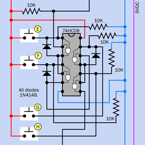
Figure 4-106. The middle section of the circuit, showing actual components.
Time to Build!
The fully breadboarded circuit is shown in Figure 4-107. For this project, you cannot really test it in stages; you have to build the whole thing. Component values are shown in Figure 4-108.
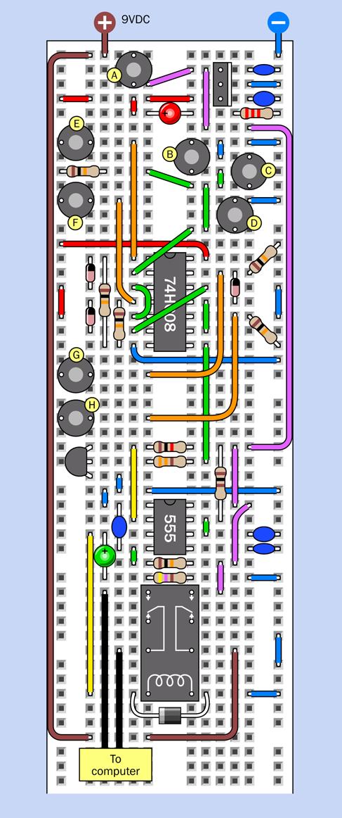
Figure 4-107. The complete breadboarded circuit for the electronic combination lock.
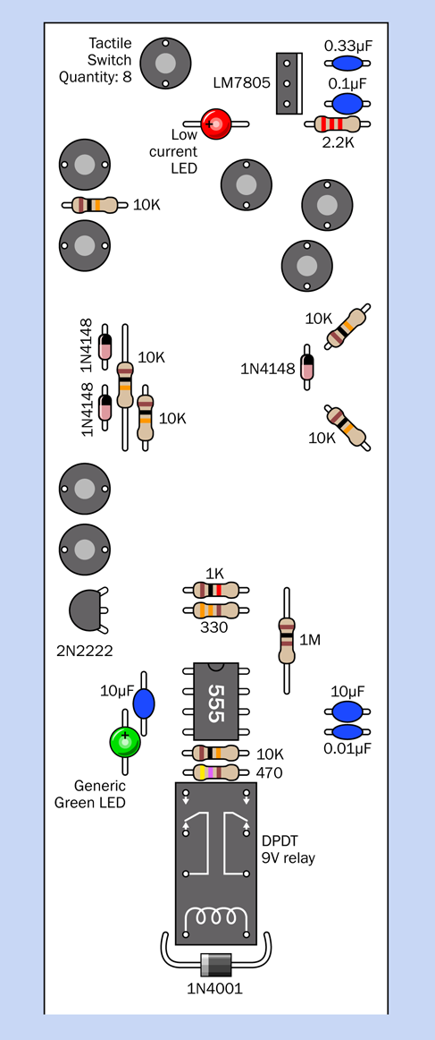
Figure 4-108. The component values for the breadboard layout.
Setup
Be careful to keep the two voltages in this circuit separate from each other. The 5VDC supply is insufficient to operate the relay, but 9VDC will burn out your logic chip. The lefthand bus on the breadboard is for the 5VDC supply. Unswitched 9VDC is taken down to the relay by the brown wire on the left of the breadboard in Figure 4-107. The purple or magenta wires on the right carry 9VDC, which is switched on either by button A or by the righthand relay contacts.
-
Brown indicates the unswitched 9VDC supply from a battery or AC adapter.
-
Magenta or purple is the 9VDC supply, which is switched, either by the relay or the button labelled A.
-
Red is 5VDC, delivered by the voltage regulator.
After you build the circuit, attach your 9VDC power supply and hold down button A. The red LED comes on, but nothing else happens.
While you continue to hold down button A, press and release each of the buttons labeled E, F, G, and H in succession, from top to bottom. When you complete the sequence, the green LED comes on, showing that the relay has closed and you successfully unlocked the circuit.
Let go of button A, and the LED should stay on for about 30 seconds before the circuit automatically switches itself off. During this 30-second period, if this circuit is installed in your computer, you will have the opportunity to start the computer.
After the circuit switches itself off, it consumes no power at all. You can run it with a 9-volt battery, and the battery should literally last for years.
Try holding the power button again, and press the same buttons in a different sequence. Also, try including some of the buttons labeled B, C, and D. The green LED will not light up, and the relay will not be activated.
Suppose you install a finished version of this circuit. To crack the code, someone will have to know:
-
You have to hold down button A while entering the correct sequence.
-
If you press an incorrect button, the code must be re-entered from the start.
-
Only buttons E, F, G, and H are active, and they must be pressed in that order.
That seems a very secure arrangement, to me. But if you want even more security, you can always add more buttons!
Testing
Set your meter to measure continuity, and attach its probes (using alligator test leads) to the lefthand output from the relay that is labeled “To Computer” in Figure 4-105. These two wires do not carry any voltage, so you need your meter in continuity-test mode to verify that the contacts inside the relay have closed.
Enter the correct combination of buttons, and the meter should beep. Let go of button A, and the meter should continue to beep while the 555 timer energizes the relay. At the end of the timer cycle, the relay opens and the meter stops beeping.
You can reconfigure your meter to measure current and insert it between the positive side of your battery and the 9VDC supply entry point on the breadboard. The meter should show no power consumption until button A is pressed.
Dealing with Diodes
This circuit contains two types of latching. The system for latching the relay is unusual but satisfies the requirement that the circuit should consume zero current when it is not being used. The system by which the AND gates latch themselves is another matter.
The fourth AND gate doesn’t need to latch, because only a brief pulse (from button H) is needed to start the timer. But the first three AND gates have to latch, to keep their outputs positive after you release each of the buttons E, F, and G. The diodes take care of this by feeding current from gate outputs back to their inputs.
Can you see any problem with this? Remember that a diode takes about 0.7 volts. Remember that a logic gate has to distinguish clearly between a high state and a low state on its inputs. If you start to sprinkle diodes through a logic circuit without keeping careful track of voltages, you may end up with a logic gate that doesn’t recognize an input that is supposed to be high. This is the same issue that I was concerned about in Experiment 15, where a voltage reduced by a transistor followed by a diode might have failed to trigger a relay.
When in doubt, verify voltages with your meter and check back to the input specifications illustrated in Figure 4-102.
In the combination-lock circuit that I’ve shown here, the output from each of the first three AND gates only circulates back through one diode to the input of the gate, so there’s no reason why this should not work reliably. Just bear in mind that you have to exercise care and discretion when mixing diodes with logic chips.
Perhaps this makes you wonder—if a diode isn’t the formally correct method to make a logic gate latch itself, what is the ideal way to do things?
One option might seem to be, replace each diode with a piece of wire, to feed the signal back to the gate input. What are the diodes really for, anyway?
They serve an important purpose. If a diode was replaced with a piece of wire, the positive voltage being applied through a pushbutton could also flow through that wire, down and around to the output of the logic gate.
-
It is absolutely not a good idea to push voltage into any output of a gate.
The correct option for latching a logic state in a circuit is with a flip-flop. Previously I have used a 555 timer wired in bistable mode as a flip-flop, because we were already working with timers, and I wanted to demonstrate this application. But in this circuit, it wouldn’t make sense to add four 555 timers just to serve that function. You can buy chips containing several flip-flops, and you can also make a flip-flop by combining two NAND gates or two NOR gates, as I will show you in Experiment 22.
For this little circuit creating a combination lock, I wanted to minimize the chip count and the complexity. Diodes were the simplest, easiest way to achieve this.
Questions
The output from the fourth AND gate was a single positive pulse. Why didn’t I use that to activate the relay directly, instead of introducing a timer?
One reason is that the relay draws an initial surge of current exceeding the maximum 20mA that an AND gate can supply. Also of course I wanted a fixed-length pulse from the timer.
All right, but why did I add a transistor to the circuit? Because the AND gate gives a positive pulse, and the timer needs a negative transition on its trigger pin. The transistor provided a way to convert a positive to a negative. Adding a NOT gate (that is, an inverter) could have achieved the same goal, but would have increased the chip count.
In that case, why didn’t I use NAND gates instead of AND gates? A NAND has a normally positive output that goes low when both of its inputs are high. That seems to be exactly what the 555 timer wants. With a NAND gate, I could have omitted the transistor.
This is true, but the preceding AND gates require positive outputs to feed back and sustain their positive inputs. So, I must retain those AND gates for the first three pushbuttons. I could only substitute a NAND gate for the last one, to create the right output for the timer. This means you would have still needed the 74HC08 chip, and you would have had to add a 74HC00 chip, just to use one of its gates. A transistor is easier and takes less room.
Here’s another question. Why did I include two LEDs in the circuit? Because when you’re punching buttons to unlock your computer, you need to know what’s going on. The Power On LED reassures you that your battery isn’t dead. The Relay Active LED tells you that the system is now unlocked, in case you are unable to hear the relay click.
Lastly, the big question: how can you actually install this circuit in a computer, assuming you are willing to give that a try? It’s a lot easier than it sounds, as I will explain.
The Computer Interface
First, make sure you have wired the combination lock circuit correctly. A single wiring error can cause your circuit to deliver 9VDC through the lefthand relay contacts instead of merely closing a switch. This is important!
To make absolutely sure, change your meter to measure volts DC, and enter the correct combination on the tactile switches. If the green LED lights up but your meter measures no voltage, this is good. Anything else, and you have a wiring error.
Now let’s consider how your computer normally functions when you want to switch it on.
Old computers used to have a big switch at the back, attached to the heavy metal box inside the computer that transformed house current to regulated DC voltages that a computer needs. Most modern computers are not designed this way; you leave the computer plugged in, and you touch a little button on the front of the computer (if it’s not a Mac) or the keyboard (if it is a Mac). The button is connected by an internal wire to the motherboard.
This is ideal from our point of view, because we don’t have to mess with high voltages. Inside your computer, don’t even think of opening that metal box with the fan mounted in it, containing the computer power supply. Just look for the wire that runs from the “power up” button to the motherboard. Most often this wire will contain just two conductors, but on some computers it will be part of a ribbon cable. The key is to look at the contacts for the pushbutton, which will be attached to the conductors that you want.
First make sure that your computer is unplugged, ground yourself (because computers contain CMOS chips that are sensitive to static electricity), and very carefully snip just one of the two conductors from the pushbutton. Now plug in your computer and try to use the “power up” button. If nothing happens, you’ve probably cut the right wire. Even if you cut the wrong wire, it still prevented your computer from booting, which is what you want, so you can use it anyway.
Remember, we are not going to introduce any voltage to this wire. We’re just going to use the relay as a switch to reconnect the conductor that you cut. You should have no problem if you maintain a cool and calm demeanor, and look for that single wire that starts everything. Check online for the maintenance manual for your computer if you’re really concerned about making an error.
After you find the wire and cut just one of its conductors, keep your computer unplugged during the next steps.
Find where the wire attaches to the motherboard. Usually there’s a small unpluggable connector. First, mark it so that you know how to plug it back in the right way around. Better still, photograph it. Then disconnect it while you follow the next couple of steps.
Strip insulation from the two ends of the wire that you cut, and solder an additional piece of two-conductor wire, as shown in Figure 4-109, with heat-shrink tubing to protect the solder joints. (This is very important!)
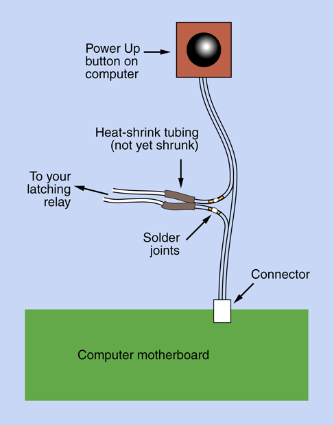
Figure 4-109. The combination lock project can be interfaced with a typical desktop computer by cutting one conductor in the wire from the “power up” pushbutton, soldering an extension, and covering the joints with heat-shrink tubing.
Run your new piece of wire to the relay, making sure you attach it to the pair of contacts that close, inside the relay, when it is energized by the unlocking operation. You don’t want to make the mistake of unlocking your computer when you think you’re locking it, and vice versa.
Reconnect the connector that you disconnected from your motherboard, plug in your computer, and press the computer’s “start” button. If nothing happens, this is good! Now enter the secret combination on your keypad (while holding down the power button to provide battery power) and watch for the green LED to light up. Now try the “start” button again, and everything should work—so long as you press the button within the 30 seconds allowed by your circuit.
Having tested your circuit, the only remaining task is installation. Just remember to remove the case completely from the rest of the computer, if you are contemplating something along the lines shown in Figure 4-110.

Figure 4-110. An option for installing your keypad (not necessarily recommended).
Enhancements
At the end of any project, there’s always more you can do.
Using a Keypad. In the previous edition of this book, I suggested using a numeric keypad in this project. Some people felt that the keypad cost too much, and others had difficulty finding the right kind of keypad. After some thought, I decided just to use tactile switches this time around. They’re easy to install on your breadboard, and if you decide to make a more permanent version of the circuit, you can simply mount eight pushbuttons on a square of metal or plastic. But a keypad is still an option, so long as it is not matrix encoded. That kind of keypad is really designed for use with a microcontroller. The kind you want will have as many pins as there are buttons, plus one.
Powering the Relay. You may be wondering if the voltage from the output of a 555 timer is sufficient to work the relay reliably. This is the same question that I discussed in Experiment 15, where I decided not to power a relay through a transistor-diode combination. The problem is, the voltage from a 555 timer varies depending on how heavily you load the output. This is why I recommended a high-sensitivity relay for this experiment. Typically it will draw less than one-third of the current of a standard type, which I felt was satisfactory for demonstration purposes. Bear in mind, I wanted to specify just one type of relay for all the experiments in this book. However, if you plan to install the circuit, and it absolutely positively has to work every time, even when your 9V battery is running low—you could consider substituting a 6VDC relay. Really? Won’t the timer output overload it? Not necessarily. Some relays are designed to tolerate overvoltage. For instance, the datasheet for the Omron G5V-2-H1-DC6 6-volt relay allows a maximum voltage of 180% of the rated voltage. As always, the best recommendation is to test a circuit thoroughly, consider options, and read datasheets.
Safeguarding the Computer. To make this project more secure, you could remove the usual screws that secure the case of the computer, and replace them with tamper-proof screws. Naturally, you will also need the special tool that fits the screws, so that you can install them (or remove them, if your security system malfunctions for any reason).
Code Update. Another enhancement would be a way to facilitate changing your secret code if you feel the need. This will be difficult if you make a soldered version of the circuit, but you can install miniature plugs and sockets known as “headers” to allow you to swap the wires around.
Destructive Security. For those who are absolutely, positively, totally paranoid, you could fix things so that entering a wrong code flips a second high-amperage relay which supplies a massive power overload, melting your CPU and sending a big pulse through the hard drive. For a solid-state drive, you could consider installing a “suicide relay” that will apply a higher voltage to the 5VDC input. But I wouldn’t recommend this myself.
There’s no doubt about it. Messing up the hardware has major advantages compared with trying to erase data using software. It’s faster, difficult to stop, and tends to be permanent. So, when the Recording Industry Association of America comes to your home and asks to switch on your computer so that they can search for illegal file sharing, just accidentally give them an incorrect unlocking code, sit back, and wait for the pungent smell of melting insulation—or a burst of gamma rays, if you go for the nuclear option (see Figure 4-111).

Figure 4-111. For those who are absolutely, positively, totally paranoid: a meltdown/self-destruct system controlled by a secret key combination provides enhanced protection against data theft or intrusions by RIAA investigators asking annoying questions about file sharing.
On a more realistic level, no system is totally secure. The value of a hardware locking device is that if someone does defeat it (for instance, by figuring out how to unscrew your tamper-proof screws, or simply ripping your keypad out of the computer case with metal shears), at least you’ll know that something happened—especially if you put little dabs of paint over the screws to reveal whether they’ve been messed with. By comparison, if you use password-protection software and someone defeats it, you may never know that your system has been compromised.
Experiment 22: Race to Place
The next project using digital logic is going to get us into the concept of feedback, where the output is piped back to affect the input—in this case, blocking it. It’s a small project, but quite subtle, and the concepts will be useful to you in the future.
What You Will Need
-
Breadboard, hookup wire, wire cutters, wire strippers, multimeter
-
9-volt power supply (battery or AC adapter)
-
74HC32 logic chip (1)
-
555 timers (2)
-
SPDT slide switches (2)
-
Tactile switches (2)
-
Resistors: 220 ohms (1), 2.2K (1), 10K (3)
-
Capacitors: 0.01µF (2), 0.1µF (1), 0.33µF (1)
-
LM7805 voltage regulator (1)
-
Generic LEDs (2)
-
Low-current LED (1)
The Goal
On quiz shows such as Jeopardy!, contestants race to answer each question. The first person who hits an answer button automatically locks out the other contestants, so that their buttons become inactive. How can we make a circuit that will do the same thing?
If you search online, you’ll find several hobby sites where other people have suggested circuits to work this way, but they lack features that I think are necessary. The approach I’m going to use here is both simpler and more elaborate. It’s simpler because it has a very low chip count, but it’s more elaborate in that it incorporates “quizmaster control” to make a more realistic game.
I’ll suggest some initial ideas for a two-player version. After I develop that idea, I’ll show how it could be expanded to four or even more players.
A Conceptual Experiment
I want to show how this kind of project grows from an initial idea. By going through the steps of developing a circuit, I’m hoping I may inspire you to develop ideas of your own in the future, which is much more valuable than just replicating someone else’s work.
First consider the basic concept: there are two people, each with a button to press, and whoever goes first locks out the other person.
Sometimes it helps me to visualize this kind of thing if I draw a sketch, so that’s where I’ll begin. In Figure 4-112, the signal from each button passes through an imaginary component that I’ll call a “button blocker,” activated by the other person’s button. I’m not exactly sure what the button blocker will be or how it will work, yet, but it will be activated by one player going first, and it will block the other player.
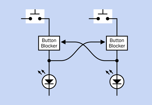
Figure 4-112. The basic concept: whoever goes first blocks the other player.
Now that I’m looking at it, I see a problem here. If I want to expand this to three players, it will get complicated, because each player must activate the “button blockers” of two opponents, and if there are four players, each much activate the “button blockers” of three opponents. The number of connections will become unmanageable. Figure 4-113 shows this.
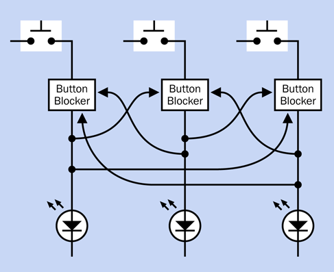
Figure 4-113. Increasing the number of participants from two to three more than doubles the number of connections.
Any time I see this kind of complexity, I think there has to be a better way.
Also, there’s another problem. After a player lets his finger off the button, the other players’ buttons will be unblocked again. This suggests to me that as in Experiments 15, 19, and 21, I need . . . a flip-flop, also known as a latch. Its purpose will be to hold the signal from the first player’s button and continue to block the other players, even after the first player has released his button.
This now sounds even more complicated. But wait a minute. If the winning player’s button triggers a latch, the latch now keeps the winning circuit energized, and the winner’s button becomes irrelevant. So, the latch can block all the buttons. This makes things much simpler. I can summarize it as a sequence of events:
-
First player presses his button.
-
His signal is latched.
-
The latched signal feeds back and blocks all the buttons.
The new sketch in Figure 4-114 shows this. Now the configuration is modular, and can be expanded to almost any number of players, just by adding more modules, without increasing in complexity.
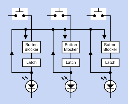
Figure 4-114. Any latch now blocks all the buttons.
There’s something important missing, though: a reset switch, to put the system back to its starting mode after the players have had time to press their buttons and see who won. Also, I need a way to prevent players from pressing their buttons too soon, before the quizmaster has finished asking the question. Maybe I can combine this function in just one switch, which will be under the quizmaster’s control.
See Figure 4-115. In its Reset position, the quizmaster switch can reset the system and remove power to the buttons. In its Set position, the switch stops holding the system in reset mode, and provides power to the buttons. I’ve gone back to showing just two players, to make everything as simple as possible, but the concept is still easily expandable.
Now I have to deal with a logic problem in the diagram. The way I’ve drawn it, everything is joined together. I’ve used arrows to show the direction of signals, but I don’t know how I could actually stop signals from going the wrong way. If I don’t deal with this, the signal from either player will light up both LEDs. How can I stop this from happening?
I could put diodes in the “up” wires to block current from running down them. But I have a more elegant idea: I’ll add an OR gate, because the inputs to an OR gate are separated from each other electrically. Figure 4-116 shows this.
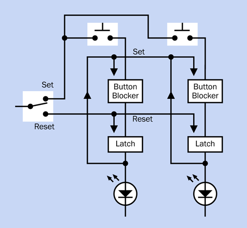
Figure 4-115. Quizmaster control has now been added.
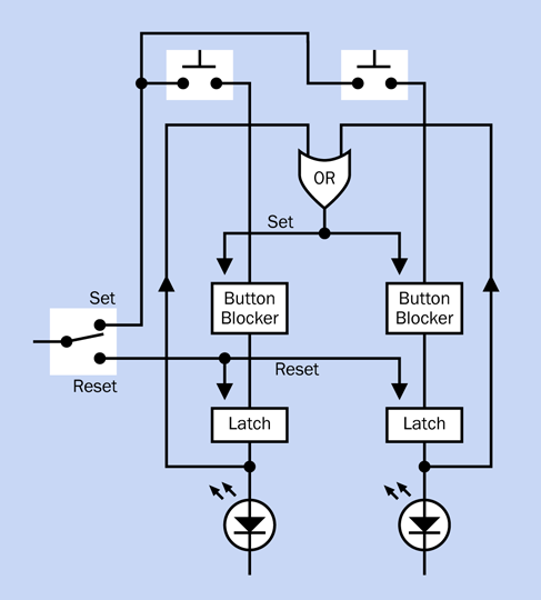
Figure 4-116. Adding an OR gate isolates one player’s circuit from the other.
The basic OR gate has only two logical inputs. Will this prevent me from adding more players? No, because you can buy an OR that has three, four, or even eight inputs. If any one of them is high, the output is high. For fewer players than a gate can handle, you tie the unused inputs to ground and ignore them.
Now I’m getting a clearer idea of what the thing I’ve called a “button blocker” should actually be. I think it should be another logic gate. It should say, “If there’s only one input, from a button, I’ll let it through. But if there are any additional inputs, I won’t let them through.”
Before I start choosing gates, though, I have to decide what the latch will be. I can buy an off-the-shelf flip-flop, which flips “on” if it gets one signal and “off” if it gets another, but chips containing flip-flops tend to have more features than I need for a simple circuit like this. Therefore I’m going to use 555 timers again, in bistable mode. They require very few connections, work very simply, and can deliver a good amount of current to drive bright LEDs. The only problem with them is that 555s in bistable mode require:
-
Negative trigger input to create a high output
-
Negative reset input to create a low output
All right, so, each player’s button will have to generate a negative pulse instead of a positive pulse. That will suit the requirements of the timers.
Finally, here’s a simplified schematic, in Figure 4-117. I like to show the pins of the 555 timers in their correct positions, so I had to move the components around a little to minimize wire crossovers, but you can see that logically, it’s the same basic idea.
I didn’t have enough room to add positive and negative symbols to show which timer pins are being held in each state, so a red circle means that the pin is being held in a high state, and a blue circle shows that it is being held in a low state. Black circles mean that the pin states may change. White circles mean that the states of these pins are not important, and the pins can be left unconnected.
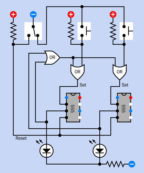
Figure 4-117. A preliminary logic diagram. Blue pins on the timers are held in a low state, red pins are held in a high state, and white pins are not relevant.
Before you try to build it, just run through the theory of it, because that’s the final step, to make sure there are no mistakes. The important thing to bear in mind is the 555 needs a negative input on its trigger pin to create a positive output. This means that when any of the players presses a button, the button has to create a negative “flow” through the circuit.
This is a bit counterintuitive, so I’m including a four-step visualization in Figure 4-118, Figure 4-119, Figure 4-120, and Figure 4-121, showing how it will work.
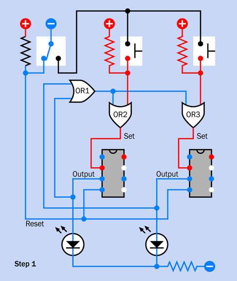
Figure 4-118. Step 1 in the circuit visualization. Reset mode.
In Step 1, the quizmaster’s switch is in reset mode. The low voltage on the reset pins of the timers has forced them both to create negative outputs. These outputs keep the LEDs dark and also go to the OR1 gate. Because it has negative inputs, it creates a negative output, although OR2 and OR3 ignore that because one input on each of these gates is high, provided by pullup resistors beside the buttons. Remember, if either of the inputs to an OR gate is high, the output is high. And so long as the trigger pin on a timer in bistable mode is high, the timer will not be triggered. So, the circuit is stable.
In Step 2, the quizmaster has asked a question and flipped his switch to the right, to supply (negative) power to the players’ buttons. However, neither of the players has responded yet, so the pullup resistors maintain the circuit in a stable state with negative outputs from the timers.
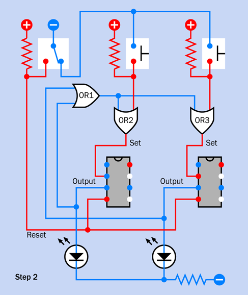
Figure 4-119. Step 2 in the circuit visualization. Players’ buttons are active, but no one has pressed a button yet.
In Step 3, Player 1 has pressed the lefthand button. This sends a low pulse to OR2. Now that OR2 has two low inputs, its output goes low. The low pulse goes to the trigger pin of the lefthand timer. But components do not respond instantaneously, and the timer has not processed the signal yet.
In Step 4, a few microseconds later, the timer has processed the negative input signal and created a positive output pulse that lights the LED and also circulates back to OR1. Now that OR1 has a positive input, it also has a positive output. This goes to the inputs of OR2 and OR3, and so their outputs become positive. As a result, both of the timers now have positive inputs on their trigger pins. Any button press by either player will now be ignored, because OR1 continues to supply positive current in the circuit.
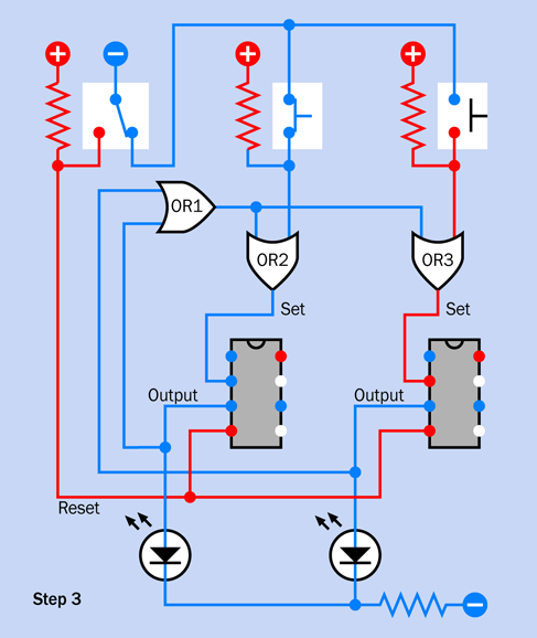
Figure 4-120. Step 3 in the circuit visualization. The left player has pressed a button, but the 555 timer has not responded yet.
-
Remember, when a 555 is running in flip-flop mode, a low input on its trigger pin will flip it into having a high output, and the output will persist even if the trigger pin goes high again.
-
The only thing that will end the 555’s high output is a low state on its reset pin. That will only happen when the game master turns his switch back to reset mode.
There’s only one situation that can upset this happy scenario. What if both players press their buttons absolutely simultaneously? In the world of digital electronics, this is highly unlikely. But if it somehow happens, both of the timers should react, and both of the LEDs will light up, showing that there has been a tie.
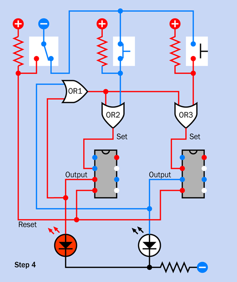
Figure 4-121. Step 4 in the circuit visualization. The left player’s action has flowed through the circuit and now blocks the right player.
On the Jeopardy! TV show, you never see a tie. Absolutely never! I’m wondering, if the electronic system on the show registers a simultaneous response from two players, maybe it has a randomizing feature to select one of them. Just speculating, of course.
To demonstrate how a two-player circuit can be upgraded to handle extra players, I’ve included a simplified three-player schematic in Figure 4-122. The circuit could be extended outward indefinitely, the only limit being the number of inputs available on OR1.
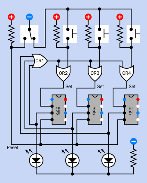
Figure 4-122. The circuit can be expanded easily for more players.
Breadboarding It
In Figure 4-123 I have revised the schematic using an actual OR chip, in a layout as close to a breadboard configuration as possible, so that you can build this thing easily. A breadboarded version is shown in Figure 4-124, and the component values are shown in Figure 4-125.
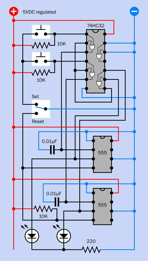
Figure 4-123. The two-player schematic has been redrawn here, using a quad two-input OR chip.
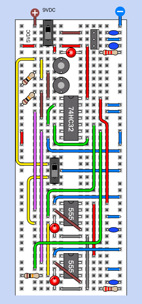
Figure 4-124. Breadboard layout, equivalent to the schematic.
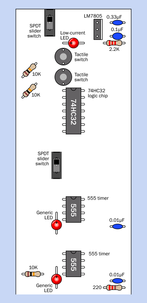
Figure 4-125. Component values for the breadboard layout.
Because the only logic gates that I’ve used are OR gates, and only three are needed, I just need one logic chip: the 74HC32, which contains four two-input OR gates. (I’ve grounded the inputs to the fourth). The two OR gates on the left side of the chip have the same functions as OR2 and OR3 in my simplified schematic, and the OR gate at the bottom-right side of the chip works as OR1, receiving input from pin 3 of each 555 timer. If you have all the components, you should be able to put this together and test it quite quickly.
You may notice that I’ve added a 0.01µF capacitor between pin 2 of each 555 timer (the input) and negative ground. Why? Because when I tested the circuit without the capacitors, sometimes I found that one or both of the 555 timers would be triggered simply by flipping the quizmaster switch, without anyone pressing a button.
At first this puzzled me. How were the timers getting triggered, without anyone doing anything? Maybe they were responding to “bounce” in the quizmaster switch—meaning tiny and very rapid vibrations in the contacts when the switch is moved. Sure enough, this was happening, and small capacitors solved the problem. They may also slow the response of the 555 timers fractionally, but not enough to interfere with slow human reflexes.
As for the buttons, it doesn’t matter if they “bounce,” because each timer locks itself on at the very first impulse and ignores any hesitations that follow.
You can experiment building the circuit, disconnecting the 0.01µF capacitors, and flipping the quizmaster switch to and fro a dozen times. Because I am recommending a small, cheap slide switch, I think you will see a number of “false positives.” I’m going to explain more about switch bounce, and how to get rid of it, in the next experiment.
Enhancements
After you breadboard the circuit, if you proceed to build a permanent version, I suggest that you expand it so that at least four players can participate. This will require an OR gate capable of receiving four inputs. The 74HC4078 is the obvious choice, as it allows up to eight. Just connect any unused inputs to negative ground.
Alternatively, if you already have a couple of 74HC32 chips and you don’t want to bother ordering a 74HC4078, you can gang together three of the gates inside a single 74HC32 so that they function like a four-input OR. Look at the simple logic diagram in Figure 4-126 showing three ORs, and remember that the output from each OR will go high if at least one input is high.

Figure 4-126. Three two-input ORs can emulate a single four-input OR.
And while you’re thinking about this, can you figure out how to combine three two-input ANDs that will substitute for a four-input AND gate?
For a four-player game, you’ll need two additional 555 timers, of course, and two more LEDs, and two more pushbuttons.
As for creating a schematic for the four-player game—I’m going to leave that to you. Begin by sketching a simplified version, just showing the logic symbols. Then convert that to a breadboard layout (which is the hard part). And here’s a suggestion: pencil, paper, and an eraser can still be quicker, initially, than circuit-design software or graphic-design software, in my opinion.
Experiment 23: Flipping and Bouncing
In three experiments, now, I’ve used 555 timers in bistable mode. The time has come to deal with “real” flip-flops, including an explanation of how they work. I will also show how they can deal with the phenomenon that I mentioned briefly in the previous experiment: switch bounce.
When a switch is flipped from one position to another, its contacts vibrate very briefly. This is the “bounce” of which I speak, and it can be a problem in circuits where digital components respond so quickly, they interpret every tiny vibration as a separate input. If you connect a pushbutton to the input of a counter chip, for instance, the counter may register 10 or more input pulses from a single press of the button. A sample of actual switch bounce is shown in Figure 4-127.
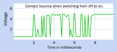
Figure 4-127. Fluctuations created by vibrating contacts when a switch is closed. (Derived from a datasheet at Maxim Integrated corporation.)
There are many techniques for debouncing a switch, but using a flip-flop is probably the most fundamental.
What You Will Need
-
Breadboard, hookup wire, wire cutters, wire strippers, multimeter
-
9-volt power supply (battery or AC adapter)
-
74HC02 logic chip (1), 74HC00 logic chip (1)
-
SPDT slide switches (2)
-
Low-current LEDs (3)
-
Resistors: 680 ohms (2), 10K (2), 2.2K (1)
-
Capacitors: 0.1µF (1), 0.33µF (1)
-
LM7805 voltage regulator (1)
Assemble the components on your breadboard, as shown in Figure 4-128. The same circuit is shown as a schematic in Figure 4-129, and the component values are shown in Figure 4-130. When you apply power, one of the LEDs at the bottom should be lit.
Now I want you to do something odd. Please disconnect the wire labeled A in Figure 4-128. Just pull it out of the board. If you refer to the schematic in Figure 4-129, you’ll see that you have disconnected power to the pole of the switch, leaving the two NOR gates connected only with their pulldown resistors.
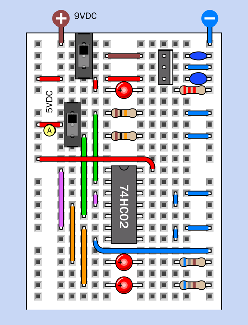
Figure 4-128. Breadboarded flip-flop circuit using NOR gates.
You may be surprised to find that the LED remains lit.
Push the wire back into the board, slide the switch to its opposite position, and the first LED should go out, while the other LED should come on. Once again, pull out the wire, and once again, the LED should remain lit.
Here’s the take-home message:
-
A flip-flop requires only an initial input pulse—for example, from a switch.
-
After that, it ignores that input.
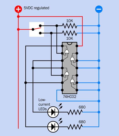
Figure 4-129. Flip-flop schematic using NOR gates.
How It Works
Two NOR gates or two NAND gates can function as a flip-flop.
-
Use NOR gates when a double-throw switch delivers a positive input.
-
Use NAND gates when a double-throw switch delivers a negative input.
Either way, you have to use a double-throw switch.
I’ve mentioned the double-throw switch three times (actually, four times if you count this sentence) because for some strange reason, most introductory books fail to emphasize this point. When I first started learning electronics, I went crazy trying to understand how two NORs or two NANDs could debounce a simple SPST pushbutton—until finally I realized that they can’t. The reason is that when you power up the circuit, the NOR gates (or NAND gates) need to be told in which state they should begin. Their initial orientation comes from the switch being in one state or the other. A SPST pushbutton cannot do that, when it is not being pushed. So you have to use a double-throw switch. (Now I’ve mentioned it five times.)
Figure 4-130. Component values for the breadboarded NOR-based flip-flop.
Debouncing with NORs
I’ve created a multiple-step schematic in Figure 4-131 and Figure 4-132 to show the changes that occur as a switch flips to and fro with two NOR gates. To refresh your memory, I’ve also included a truth table in Figure 4-133 showing the logical outputs from NOR gates for each combination of inputs.
Referring initially to Figure 4-131, in Step 1, the switch is supplying positive current to the lefthand side of the circuit, overwhelming the negative supply from the pulldown resistor, so we can be sure that the NOR gate on the left has one positive logical input. Because any positive logical input will make the NOR give a negative output (as shown in the truth table in Figure 4-133), the negative output crosses over to the righthand NOR, so that it now has two negative inputs, which make it give a positive output. This crosses back to the lefthand NOR gate. So, in this configuration everything is stable.
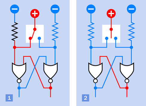
Figure 4-131. When the switch moves to a neutral center position, the status of the NOR gates remains unchanged.
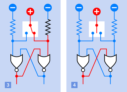
Figure 4-132. After the states of the NOR gates are reversed, they remain that way when the switch moves back to its neutral center position.
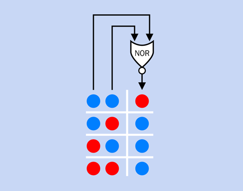
Figure 4-133. A reminder of the truth table for a NOR gate.
Now comes the clever part. In Step 2, suppose that you move the switch so that it doesn’t touch either of its contacts. (Or suppose that the switch contacts are bouncing, and failing to make a good contact. Or suppose you disconnect the switch entirely.) Without a positive supply from the switch, the lefthand input of the left NOR gate goes from positive to negative, as a result of the pulldown resistor. But the righthand input of this gate is still positive, and one positive is all it takes to make the NOR maintain its negative output, so nothing changes. In other words, the circuit has “flopped” in this state, regardless of whether the switch is disconnected.
Referring to Figure 4-133, if the switch turns fully to the right and supplies positive power to the righthand pin of the right NOR gate, that NOR recognizes that it now has a positive logical input, so it changes its logical output to negative. That goes across to the other NOR gate, which now has two negative inputs, so its output goes positive, and runs back to the right NOR.
In this way, the output states of the two NOR gates change places. They flip, and then flop there, even if the switch breaks contact or is disconnected again, as in Step 4.
If a switch bounces so severely that the pole connection fluctuates all the way between one contact and the other, this circuit won’t work. It only works if the output alternates between one connection, and no connection at all. But this is generally the case with a SPDT switch.
Debouncing with NANDs
The drawings in Figure 4-134 and Figure 4-135 show a similar sequence of events if you use a negatively powered switch with two NAND gates. To refresh your memory of NAND behavior, I am including Figure 4-136.
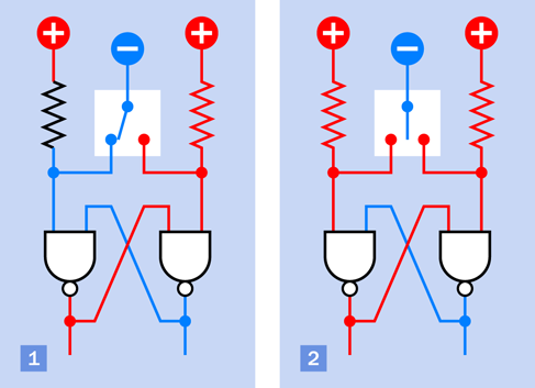
Figure 4-134. Two NAND gates can be used as a flip-flop with pullup resistors and a switch providing negative power.
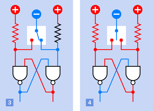
Figure 4-135. Once again, the gate states remain unchanged when the switch is unconnected with either of them.

Figure 4-136. A reminder of the truth table for a NAND gate.
If you want to verify the function of the NAND circuit, you can use your 74HC00 chip, specified in the parts list for this experiment, to test it yourself. Be careful, though: the gates inside the NOR chip are upside-down compared with the gates inside the NAND chip. You will have to move some wires around on your breadboard, because the two chips are not swappable. Refer back to Figure 4-83 and Figure 4-95 for the specifications.
Jamming Versus Clocking
The NOR and the NAND circuits are examples of a jam-type flip-flop, so called because the switch forces it to respond immediately, and jams it into that state. You can use this circuit anytime you need to debounce a switch (as long as it’s a double-throw switch).
A more sophisticated version is a clocked flip-flop, which requires you to set the state of each input first and then supply a clock pulse to make the flip-flop respond. The pulse has to be clean and precise, which means that if you supply it from a switch, the switch must be debounced—probably by using another jam-type flip-flop! Considerations of this type have made me reluctant to use clocked flip-flops in this book. They add a layer of complexity that I prefer to avoid in an introductory text. If you want to know more about flip-flops, I explore them in greater detail in Make: More Electronics. It’s not a simple topic.
What if you want to debounce a single-throw button or switch? Well, you have a problem! One solution is to buy a special-purpose chip such as the 4490 “bounce eliminator,” which contains digital delay circuitry. A specific part number is the MC14490 from On Semiconductor. This contains six circuits for six separate inputs, each with an internal pullup resistor. It’s relatively expensive, however—more than 10 times the price of a 74HC02 containing NOR gates. Really, you will have an easier time if you avoid single-throw switches and use double-throw switches (or pushbuttons) that are more easily debounced.
Or, you could use a 555 timer wired in flip-flop mode. My preference for that option now seems to make more sense.
Experiment 24: Nice Dice
Electronic circuits to simulate the throw of one or two dice have been around for decades. However, new configurations still exist, and this project provides an opportunity to learn more about logic while ending up with something useful. I especially want to introduce you to binary code, the universal language among digital chips.
What You Will Need
-
Breadboard, hookup wire, wire cutters, wire strippers, multimeter
-
9-volt power supply (battery or AC adapter)
-
555 timer (1)
-
74HC08 logic chip (1), 74HC27 logic chip (1), 74HC32 logic chip (1)
-
74HC393 binary counter (1)
-
Tactile switch (1)
-
SPDT slide switches (2)
-
Resistors: 100 ohms (6), 150 ohms (6), 220 ohms (7), 330 ohms (2), 680 ohms (4), 2.2K (1), 10K (2), 1M (1)
-
Capacitors: 0.01µF (2), 0.1µF (2), 0.33µF (1), 1µF (1), 22µF (1)
-
LM7805 voltage regulator (1)
-
Low-current LEDs (15)
-
Generic LED (1)
A Binary Counter
At the heart of every electronic dice circuit that I have ever seen is a counter chip of some kind. Often it’s a decade counter with 10 “decoded” output pins that are energized one at a time, in sequence. A die only has six faces, but if you tie the seventh pin of the counter back to its reset pin, the counter will restart after it reaches six. (Note that “dice” is really a plural word that should only be used for two dice or more, while “die” is the singular word, although many people don’t realize this.)
I always like to do things differently, so I decided not to use a decade counter, partly because I wanted a binary counter to satisfy my desire to demonstrate binary code. This added a little complexity to the circuit, but will enrich the learning process—and when all is said and done, you’ll have a circuit that runs two dice (not just one) with a modest chip count, while still fitting on a breadboard.
The counter chip that I’ve chosen is widely used: the 74HC393. It actually contains two counters, but the second one can be ignored for the time being. The pinouts are shown in Figure 4-137.
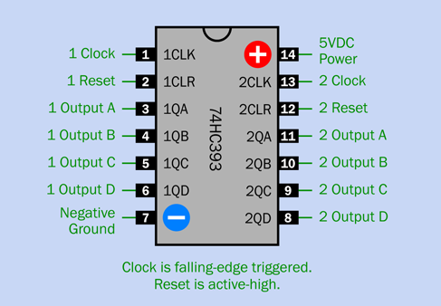
Figure 4-137. Pin functions of the 74HC393 binary counter.
Manufacturers have an odd habit of identifying the pin functions of digital chips using as few letters as possible. These cryptic abbreviations can be difficult to understand. To give you an example, in Figure 4-137 the pin labels inside the outline of the chip are the ones I found in a datasheet from Texas Instruments. (To make things even more confusing, other manufacturers use different abbreviations of their own. There is no standardization.)
Outside the outline of the counter I have restated the pin functions in relatively plain English, in green lettering. The number preceding each pin function refers to counter #1 or counter #2, packaged separately in the chip.
Counter Testing
The best way to understand this chip is to bench-test it. Figure 4-138 shows the schematic, and Figure 4-139 shows it on a breadboard. Figure 4-140 shows the breadboarded component values.
Remember:
-
This is a 5V logic chip. Don’t leave out the voltage regulator.
-
Note there is a 0.1µF capacitor between the power-supply pin of the timer, and ground. This is to suppress little voltage spikes that the timer tends to generate. They can confuse the counter if they are uncontrolled.
The capacitor and resistors that I have specified with the timer will run at about 0.75Hz. In other words, the beginning of one pulse, and the beginning of the next pulse, will be slightly more than one second apart. You can see this by watching the yellow LED on the timer output. (If the yellow LED does not behave this way, you made a wiring error somewhere.)
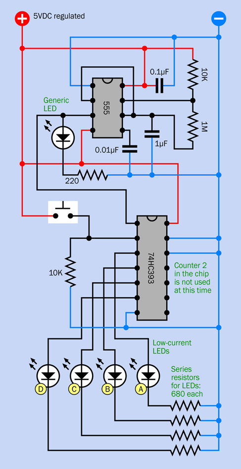
Figure 4-138. Schematic for observing the output and the reset function of the 74HC393 decade counter.
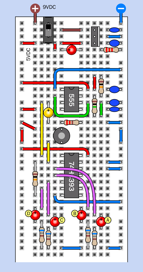
Figure 4-139. The breadboarded test circuit.
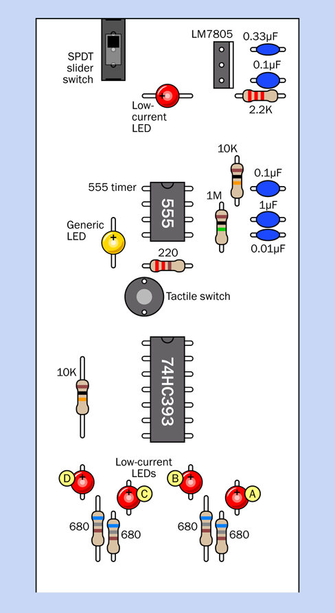
Figure 4-140. Component values in the breadboarded circuit.
The four red LEDs labeled A, B, C, and D will display the output states of the counter. If your connections are correct, they will run through the sequence shown in Figure 4-141, where a black circle indicates that an LED is not lit, and a red circle indicates that it is lit.
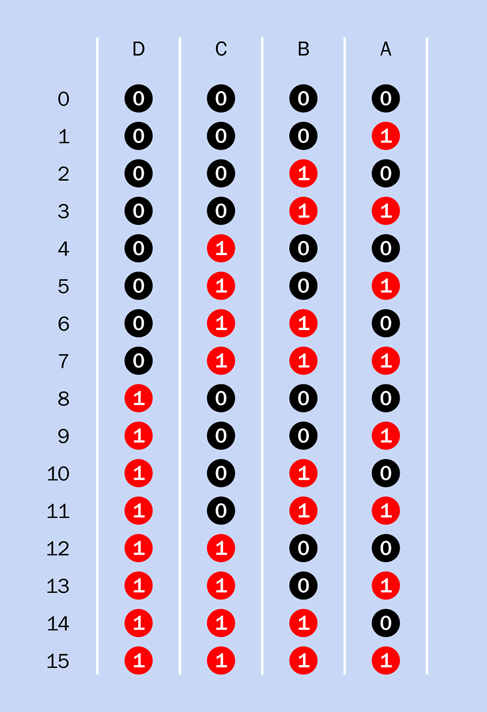
Figure 4-141. The full sequence of outputs from a binary counter.
I’m going to tell you some more, now, about binary and decimal arithmetic. Do you really need to know this? Yes, it’s useful. A variety of chips such as decoders, encoders, multiplexers, and shift registers use binary arithmetic, and of course it is absolutely fundamental in almost every digital computer that has ever been made.
Fundamentals: Binary Code
As you can see in Figure 4-141, every time the LED in column A goes out, the LED in column B reverses its state—from on to off, or off to on. Every time the LED in column B goes out, it reverses the LED in column C, and so on. One consequence of this rule is that each LED flashes twice as fast as the one to its left.
The row of LEDs represents a binary number, meaning a number written in only two digits: 0 and 1, as shown in the white font in Figure 4-141. The equivalent decimal number is shown in the black font on the left.
The LEDs can be considered binary digits, commonly known as bits.
The rule for counting in binary is very simple. In the rightmost column, start with 0, then add 1—and then, because you can only count in ones and zeroes, the next time you want to add 1, you have to revert to 0 and carry 1 to the next column to the left.
What if the numeral in the next column to the left is already a 1? Change it back to 0 and carry 1 to the next column after that. And so on.
The rightmost LED represents the least significant bit of a four-bit binary number. The leftmost LED is showing us the most significant bit.
Rising Edge, Falling Edge
When you run the test, notice that each transition of the rightmost red LED (either from on to off, or off to on) always occurs when the yellow LED goes out. Why is this?
Most counters are edge triggered, meaning that the rising edge or the falling edge of a high pulse nudges the counter along to the next value in its series, when the pulse is applied to the clock input pin. The behavior of the LEDs clearly shows you that the 74HC393 is falling-edge triggered. In Experiment 19, we used a counter that was rising-edge triggered. The type that you use depends on your application.
The 74HC393 counter also has a reset pin, just like the 4026B chip from Experiment 19.
-
Some datasheets describe a reset pin as a “master reset” pin, which may be abbreviated MR.
-
Some manufacturers call a “reset” pin a “clear” pin, which may be abbreviated CLR on a datasheet.
Whatever it’s called, the reset pin will always have the same end result. It forces all the outputs of the counter to go low—which in this case means 0000 binary.
A reset pin requires a separate pulse. But does the reset occur when the pulse begins, or when it ends?
Let’s find out. If you built the circuit carefully, the reset pin is held in a low state through a 10K resistor. But there is also a tactile switch that can connect the reset pin directly to the positive bus. This overwhelms the 10K resistor, and forces the reset pin to go high.
As soon as you press the tactile switch, all the outputs go dark, and they stay dark until you let go of the tactile switch. Evidently, the reset function of the 74HC393 is triggered and held by a high state.
The Modulus
Switch off the power, disconnect the pullup resistor and the tactile switch from the reset pin (pin 2), and substitute a wire as shown in Figure 4-142. All the previous connections have been grayed out. The new wire, in solid black, connects the fourth digit, from output D, to the reset pin. Figure 4-143 shows the revision on the breadboard; the new connection is colored green.
What do you think will happen?
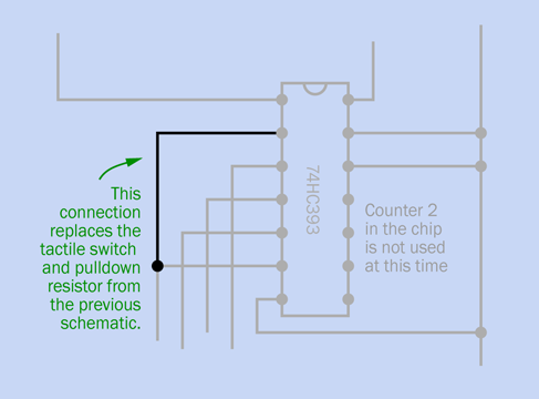
Figure 4-142. Adding an automatic reset to the timer.
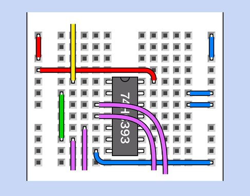
Figure 4-143. Close-up of the revision on the breadboard. The pulldown resistor, the tactile switch, and associated connections have been removed. The green wire has been inserted.
Run the counter again. It counts from 0000 up to 0111. The very next binary output should be 1000, but as soon as the fourth digit transitions from 0 to 1, the high state is sensed by the reset pin, forcing the counter back to 0000.
Can you see the leftmost LED flicker, before the counter resets? I doubt it, because the counter responds in less than a millionth of a second.
The counter now runs from 0000 through 0111 before automatically repeating itself. Because counting from 0000 through 0111 binary is equivalent to counting from 0 to 7 in decimal, we now have a divide-by-8 counter. (Previously, it was a divide-by-16 counter.)
Suppose you move your reset wire from the fourth digit to the third digit. Now you have a divide-by-4 counter.
-
You can easily wire almost any 4-bit binary counter so that it resets after 2, 4, or 8 input pulses.
The number of states in the output of a counter, before it repeats, is known as the modulus, often abbreviated as “mod.” A mod-8 counter repeats after eight pulses (which are numbered from 0 through 7).
Converting to Modulus 6
What about the project that we are supposed to be working on here, to generate electronic dice patterns? I’m getting to it. Because a die has six sides, I have a feeling that we may need to rewire the counter so that it repeats after six states.
In binary code, the output sequence will look like this: 000, 001, 010, 011, 100, 101. (We can ignore the most significant bit, in column D, because we don’t need it for just six states.) I need to make the counter reset after its output of 5 decimal, which is 101 binary.
(Why 5 decimal, and not 6 decimal? Because we are counting upward from 0. It would be more convenient in this project if the counter would start from 1, but it doesn’t do that.)
What’s the next output after 101 binary? The answer is 110 binary.
Is there something distinctive about 110? If you study the sequence, you’ll see that 110 is the first in the series that begins with two high bits.
How can we tell the counter, “When you have a 1 in column B, and a 1 in column C, reset to 0000?” The word “and” in the last sentence should give you a clue. An AND gate has a high output when, and only when, its two inputs are high. Just what we need.
Can we drop it right in? Absolutely, because all the members of the 74HCxx chip family are designed to talk to each other. In Figure 4-144 you will see that I have added an AND gate. Of course, to use it on your breadboard, you’ll have to add an appropriate chip, which is a 74HC08. It contains four AND gates, of which we only need one. Therefore, in addition to power connections, its unused inputs must be grounded. This is a bit of a hassle, but I’ll show you how to do it, as soon as I make a few more additions and modifications. (The unused outputs must be left unconnected.)
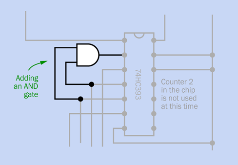
Figure 4-144. An AND gate has been added, to adjust the counter so that it only cycles through six output states instead of its usual 16.
Meanwhile, please remember this take-home message:
-
You can use logic chip(s) with a counter to change the modulus of the counter by looking for a distinctive pattern in the output states, and feeding back a signal to the reset pin.
Not Using a Seven-Segment Display
For the dice display, I could just use a seven-segment numeral that counts from 1 to 6. But this is a problem, because the counter runs from 0 through 5. I don’t see an easy way to convert 000 binary to a seven-segment numeral 1, 001 binary to a seven-segment numeral 2, and so on.
Could we make the counter skip 000 binary somehow? Er, maybe, but I’m not sure how. Perhaps by using a three-input OR gate that would feed back to the clock input to advance the counter to the next state—but then this would conflict with the usual clock signals, and it all sounds like a lot of trouble to me.
In any case, I’m not very excited by using a seven-segment numeral in this project, because it’s not visually appealing. Why not use LEDs that emulate the pattern of spots on an actual die? The sequence is shown in Figure 4-145.

Figure 4-145. The series of spot patterns to be reproduced by LEDs.
Can you figure out a way to convert the binary output from the counter to illuminate the LEDs in those patterns?
Choosing the Gates
I’ll start with the easiest option. If I connect output A from the counter (see Figure 4-138) to the LED that represents the center spot of the die, that will work out well, because the center spot is only illuminated for patterns 1, 3, and 5, and goes out for patterns 2, 4, and 6. This is exactly the way that output A behaves.
Then things get a little tricky. I need to illuminate a diagonal pair of spots for patterns 4, 5, and 6, and the other diagonal pair for 2, 3, 4, 5, and 6. But how?
Figure 4-146 shows my answer to the problem. You’ll see I have added a couple more logic gates: a three-input NOR, and a two-input OR. Alongside I have shown the sequence of binary numbers, and the spot patterns that each number creates on the die.
To make things work, I had to begin with the die showing a 6 pattern when the counter starts at 000 binary. The sequence of patterns really doesn’t matter, so long as they are all represented. They’re going to be selected at random anyway.
Figure 4-147 shows how the counter outputs light up the different patterns of spots. And just in case this still isn’t entirely clear, I have created a snapshot sequence showing high and low states in the circuit as the counter increments from 000 through 101. The snapshots are shown in Figure 4-148, Figure 4-149, and Figure 4-150.
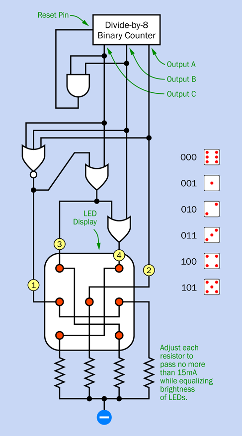
Figure 4-146. A logic network to create the sequence of spots on a die.
I squeezed the snapshots so that I could fit two into the width of a column, and I omitted the AND gate, because it doesn’t do anything during the counting range of 000 through 101. It responds only when the counter tries to advance to 110—at which point, the AND sets it back to 000.
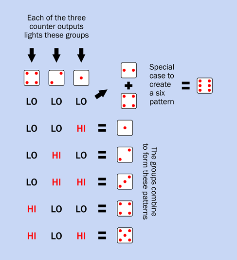
Figure 4-147. How the outputs from the binary counter are used to light the patterns of spots.
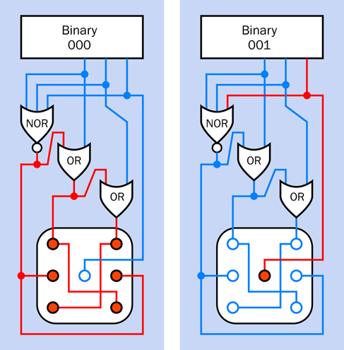
Figure 4-148. The logic for generating patterns 6 and 1.
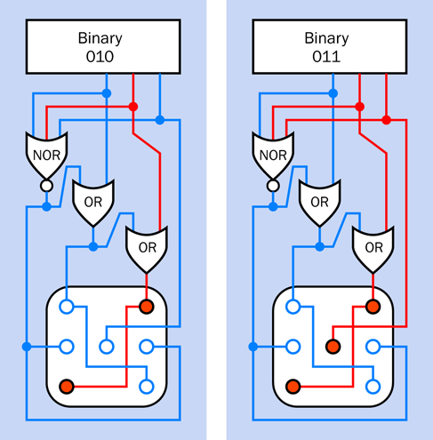
Figure 4-149. The logic for generating patterns 2 and 3.
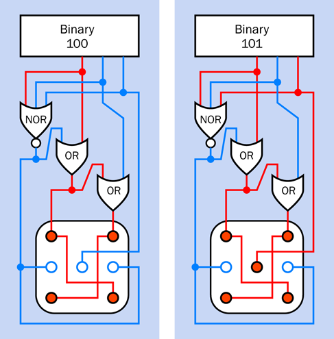
Figure 4-150. The logic for generating patterns 4 and 5.
If you’re wondering how I came up with this selection of logic gates to translate the counter output into the dice patterns, I’m not sure I know how to tell you. There’s a certain amount of trial and error, and some intuitive guesses involved in creating this kind of logic diagram. At least, that’s the way it is for me. There are more rigorous and formal ways of doing it, but personally I don’t find them so easy.
The Finished Circuit
The schematic in Figure 4-151 was derived from the logic diagram in Figure 4-146. The breadboarded version is shown in Figure 4-152.
The component values are shown in Figure 4-153. Note that I changed the timing resistor and timing capacitor for the 555 timer, so that it now runs around 5kHz. The idea of this circuit is that you will stop the timer at an arbitrary moment, after it has gone through hundreds of cycles. This way, you should end up with a random number.
I have added a switchable 22µF capacitor that can make the timer run slowly (about 2Hz) if you want to demonstrate how the counting works, to anyone who is skeptical.
I haven’t bothered to show the values for the lower half of the breadboard, because the only components there are the chips. That’s a nice aspect of building circuits based on logic: you don’t have to worry about squeezing in resistors and capacitors. Chips and wires do most of the work.
The numbered outputs at the bottom of the circuit in Figure 4-151 and Figure 4-152 correspond with the inputs to the pattern of LEDs shown in Figure 4-154. There isn’t room on the breadboard to add the LEDs, so you will either need a second breadboard, or you can drill some holes to mount the LEDs in a piece of plywood or plastic.
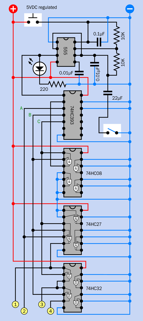
Figure 4-151. A complete circuit for emulating the roll of a single die.
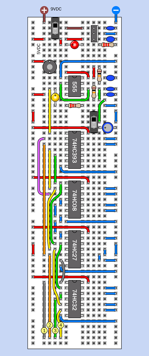
Figure 4-152. Breadboarded version of the single-die circuit.
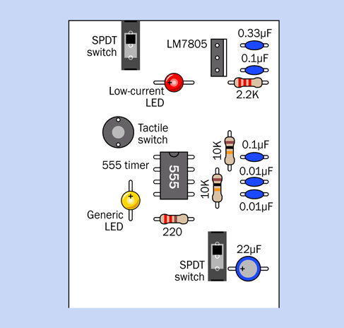
Figure 4-153. Values for the components in the control section of the dice simulation.
Three pairs of the LEDs are wired in series, because a logic chip isn’t powerful enough to drive a pair of LEDs in parallel. Putting them in series will require you to use a lower-value resistor than usual. The way to do this is to apply 5VDC to one of the pairs of LEDs through your meter, set to measure milliamps. Try a 220-ohm series resistor, and see how much current you measure. If you aim for a maximum of 15mA, that will be within the specifications of HC chip outputs. You may need a resistor with a value of 150 ohms or 100 ohms, depending on the characteristics of the LEDs that you are using.
Finally apply 5VDC through a 330-ohm resistor to the center LED, and compare its brightness to the LEDs wired in pairs. You may have to increase the resistor value to make the center LED visually equivalent to the others.
Hook up the LEDs to the logic circuit, hold down the button, release it, and you have your dice value (or, to be semantically correct, your die value).
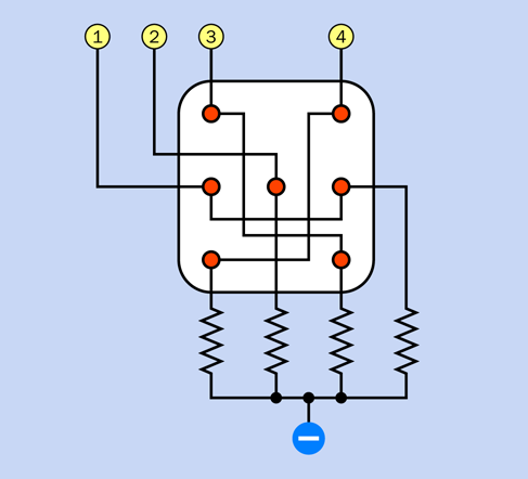
Figure 4-154. Wiring seven LEDs (six of them in pairs, in series) to display the spot patterns of a single die.
How do you know that it gives you a really random result? Really, the only way to be sure is to use it repeatedly and note how many times each number comes up. You might need to run it maybe 1,000 times to get decent verification. Because the circuit relies on the behavior of a human being pressing a button, there is no way to automate the testing process. All I can say is, the result really should be random.
Good News
There are more chips in this circuit than you’ve used in previous circuits in the book, but in the immortal words of Professor Farnsworth, in one of my favorite TV shows, Futurama: “Good news, everyone!”
The good news is that you can modify this circuit to simulate two dice instead of one, simply by adding some more wires and LEDs. You don’t need any more chips at all.
We have a lot of unused logic gates in the AND, NOR, and OR chips. Three ANDs are left over, two NORs, and two ORs. In addition, there is also an entirely separate counter in the 74HC393 chip. This is exactly what you need.
The question is, how to create a second series of random numbers, different from the first. Maybe add another 555 timer, running at a different speed?
I don’t like this idea, because the two timers will go in and out of phase with each other, and some pairs of values may come up more than others. I think it would be a better idea if the first counter runs from 000 through 101 binary, and then triggers the second counter to advance from 000 to 001. The first counter goes from 000 through 101 again, and triggers the second counter to move on to 010. And so on.
The second counter will run at one-sixth the speed of the first, but if you drive them fast enough, the patterns will still be too fast to see. The great advantage of this arrangement is that every possible combination of values will be displayed an equal number of times, so they should all have an almost-equal chance of coming up, just as if you were using two real dice.
Why do I say “almost equal”? Because, bear in mind there is a tiny delay when a counter resets itself from 101 binary to 000 binary. But if the lefthand counter is running at around 5kHz, a delay of less than one-millionth of a second seems trivial.
Chained Counters
The last remaining question is how the first counter can advance the second counter when it reaches 101 and flips back to 000.
This is easy. Consider what happens when the output from the first counter changes from 011 to 101 to 110, the last value lasting only for an instant before it resets to 000. After the C output reaches a high state, it drops low.
What does the clock input of the second counter need, to make it advance by one count? You already know that. It needs a high state that drops low. All you have to do is to connect the C output, from the first timer, to the clock input of the second timer. Indeed, the chip is designed to work this way, so that the falling state from one timer acts as a “carry” signal to advance the next timer.
The schematic in Figure 4-155 shows the circuit for two dice. I’m not including another breadboard picture, because you should be able to add the new wiring yourself. It is almost exactly a mirror image of the wiring that you already installed, but don’t forget to move it down by one row of holes on the breadboard, to allow room for the positive power supply to each chip.
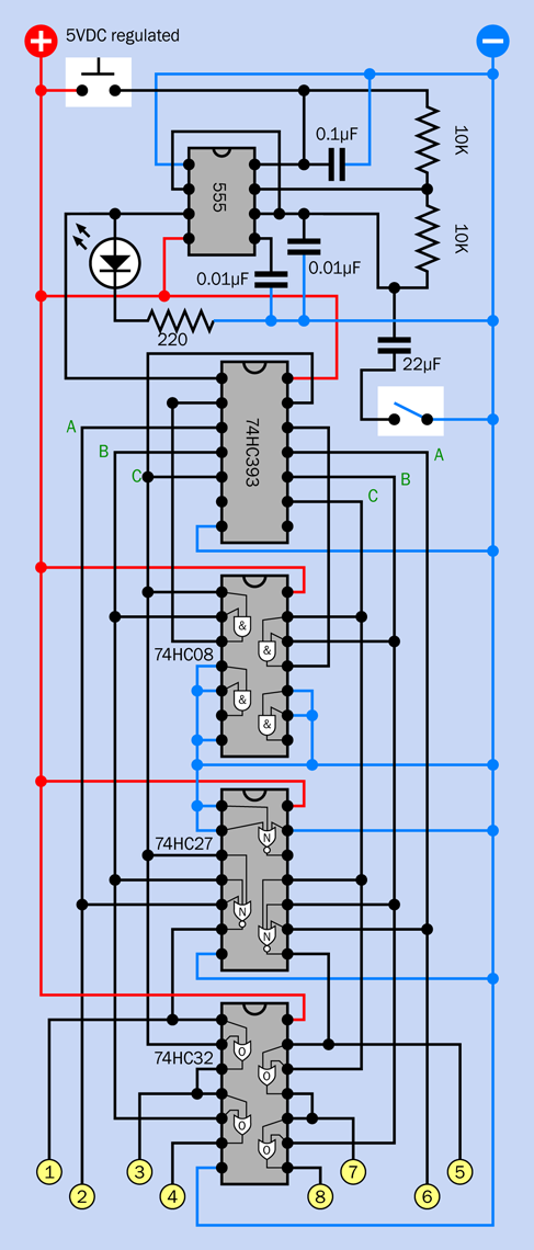
Figure 4-155. Complete circuit to run two LED dice.
Going Further
Could the circuit be simplified? As I mentioned at the beginning, a decade counter would require simpler logic than a binary counter. You wouldn’t need an AND gate to make it count with a modulus of six, because just the seventh output pin on the decade counter could be connected back to the reset.
However, if you want to run two dice, you would need two decade counters, and that would mean two separate chips. Also, you would still need two chips to handle the logic for the two displays. To see why, search online for digital dice. At this point, you should be able to understand the schematics that will be displayed in Google Images.
The only simplification I can see, in the circuit that I have described, would be to substitute two diodes for each OR gate. The circuits that you’ll find online often do this, but you will end up with a signal passing through two diodes in succession, which will drop the voltage below a level that I feel is acceptable.
The Slowdown Problem
The version of this project that I included in the first edition of Make: Electronics included a nice extra feature. When you took your finger off the “run” button, the die pattern display gradually slowed before it stopped. This increased the suspense of waiting to see what the final number would be.
The feature was enabled by splitting the power supply to the 555 timer. The timer was “always on” but voltage to its RC network was shut off when the player stopped pressing the “run” button. At that point, a large capacitor slowly discharged into the network, and the timer slowed as the voltage diminished.
A reader named Jasmin Patry sent email telling me that when he used the circuit, the value 1 came up disproportionately often, and he suspected that this had something to do with the slowdown feature.
Jasmin turned out to be a video game designer who understands much more about randomicity than I do. He had the polite, patient style of a man who really knew what he was talking about, and he seemed interested in helping to fix the problem that he had identified.
After he sent me graphs showing the relative frequency of each number in the simulation, I had to agree that the problem existed. I suggested many possible explanations, all of which turned out to be wrong. In the end Jasmin successfully proved that the lower power consumption of a single LED, relative to the higher power consumption of six LEDs, allowed the timer to keep running for a little longer when the voltage was marginal. This increased the odds that it would stop during that period.
Eventually Jasmin suggested a substitute circuit, in which a second 555 timer was added, and the outputs from the two timers were merged through an XOR gate. He successfully proved that this eliminated the bias toward one number. I was delighted that one of my readers had learned so much from reading my book, he was able to identify and fix a mistake that he found in it.
In this new edition, I have omitted the slowdown capacitor that caused the trouble in the first edition. But I haven’t adopted Jasmin’s circuit, because it was quite complicated. A single die would have needed its own pair of 555 timers, plus the XOR gate that he wanted. He also used diodes that I would have replaced with OR gates, and there wasn’t nearly enough room on the breadboard.
With his permission, I will send his circuit as a freebie to anyone who registers with me (using the procedure described in the Preface—see “Me Informing You”). I cannot easily reprint it here, because I would have to redraw it completely to fit the two-column format.
Slowdown Alternatives
You’d think there must be a simpler way to make the display slow down, without affecting the randomicity. When I looked online, I found that someone had used an NPN transistor with its emitter connected to pin 7 of the timer, and a capacitor between its base and its collector, so that when power was disconnected, the transistor output would gradually diminish. Several other people had done the same thing in their dice circuits. However, I suspect that this configuration may be subject to the same problems that Jasmin found.
I have also seen circuits using exactly the same slowdown capacitor configuration that I used (for example, on the Doctronics website). I think they are almost certainly susceptible to the problem that I have described.
My final answer on this topic may be dissatisfying: I don’t know how to achieve a slowing effect without adding more components that will greatly complicate the circuit.
However—just before the text of this book was finalized, my friend and fact-checker Fredrik Jansson suggested powering the 555 timer from a separate voltage regulator, to isolate it from power fluctuations in the rest of the circuit. I like this idea, but there wasn’t time to try it before the book went into production.
I built a completely different dice circuit using a PICAXE microcontroller, but discovered that this had its own randomicity issues because of the imperfect random-number generator built into the chip.
In Experiment 34 (the last one in this book), you’ll find that I have created yet another dice simulation, using an Arduino. But here again, I had to depend on the built-in random-number generator, and I am skeptical that it creates an evenly distributed range of numbers.
Figure 4-156. This electronic dice display uses 10mm LEDs embedded in a box of sanded polycarbonate plastic.
The issue of randomness is really not simple at all. I became so interested in it after my emails with Jasmin Patry, I explored it at length in Make: More Electronics, and also wrote a column about it in Make: magazine (volume 45) in collaboration with Aaron Logue, who runs his own little website describing projects that he builds. He introduced me to the concept of using a reverse-biased transistor to generate random noise, which is then processed with a clever algorithm attributed to the great computer scientist, John von Neumann. This, I think, is as close to a perfect random-number generator as you can get—but the chip count is not trivial.
All of these enhancements go beyond the range of an introductory-level book. If any readers have a really simple enhancement to the dice circuit presented here, to add the slowdown effect, my email inbox is always open, and yes, I do read the messages.
Meanwhile, I’m including a couple of photographs of finished electronic-dice projects. The one in Figure 4-156 was included in the first edition of this book, in 2009. Figure 4-157 shows one that I built around 1975, after Don Lancaster’s amazing TTL Cookbook told me how I could use 74xx logic chips. Forty years later, the LEDs still light up randomly. (At least, I think they’re random.)
