CHAPTER 5
SEEING AND MANIPULATING ATOMS
The difference in scale between atoms and everyday objects is enormous, and the atomic scale seems distant and hard to imagine. But thanks to an array of amazing advances in technology, it is now possible to create images of individual atoms and molecules, and even to manipulate them, one by one. Chemical reactions can be made to happen by directly breaking and making individual bonds between atoms, and the extremely rapid processes that take place in chemical reactions can be observed directly with extremely brief laser pulses.
This remarkable image shows the 27,000 or so atoms that make up a particle of platinum just 2 nanometers in diameter. It was produced by a technique called electron tomography, which involves studying the particle with a transmission electron microscope (see here) at a large number of different angles—similar to the way in which a CT (computed tomography) scan can reveal three-dimensional images of organs inside the human body. The image holds information about imperfections in the platinum crystal—information that could help to improve electronic devices, such as light-emitting diodes (LEDs).
WAYS TO SEE ATOMS
The wavelength of light is a few thousand times the size of an atom. This fact makes it impossible to see atoms in the way we see other objects: by bouncing light off them. X-rays have much shorter wavelengths, but most X-rays pass through atoms, and it is not practical to produce an X-ray microscope that can produce images. Electrons, which behave as waves as well as particles, have even smaller wavelengths than X-rays—and they can be used to produce images of individual atoms.
THE CHALLENGE OF RESOLUTION
When you look at a forest from far away, you see a blur of green and brown. You are not able to “resolve” one tree from another:;you cannot see them as two separate objects. If you move closer, you will begin to see the trees. Move closer still, and you are able to resolve individual leaves. If you hold a leaf in your hand, you can see some details on it, but your eyes cannot resolve the individual cells of which the plant is made. The resolution of the human eye is not good enough to do so. The leaf’s cells all blur into one, as the forest’s trees did from afar. The smallest objects a human eye can resolve are a little less than one-tenth of a millimeter in size (0.004 inch)—about the same size as a human egg cell.
Using a powerful microscope, it becomes possible to see all living cells, and some of the features inside them. In other words, the magnified image that a microscope produces has much greater resolution than the image formed in the naked eye, but there is a limit to the resolution of a light microscope. This limit is not technological but due to the wave nature of light. In the 1870s, German physicist Ernst Abbe discovered that it is not possible to resolve two objects separated by less than about half the wavelength of light. The shortest wavelength visible to the human eye, blue light, has a wavelength of about 4,000 Å; an atom has a diameter of only a few ångströms.
LIMITS OF VISION
The resolution of the human eye is limited by the distance at which it can clearly focus (a few inches) and how tightly packed the light-sensitive cells are in the retina. The resolution of a light microscope, on the other hand, is limited by the wave nature of light itself. After: © Johan Jarnestad/The Royal Swedish Academy of Sciences
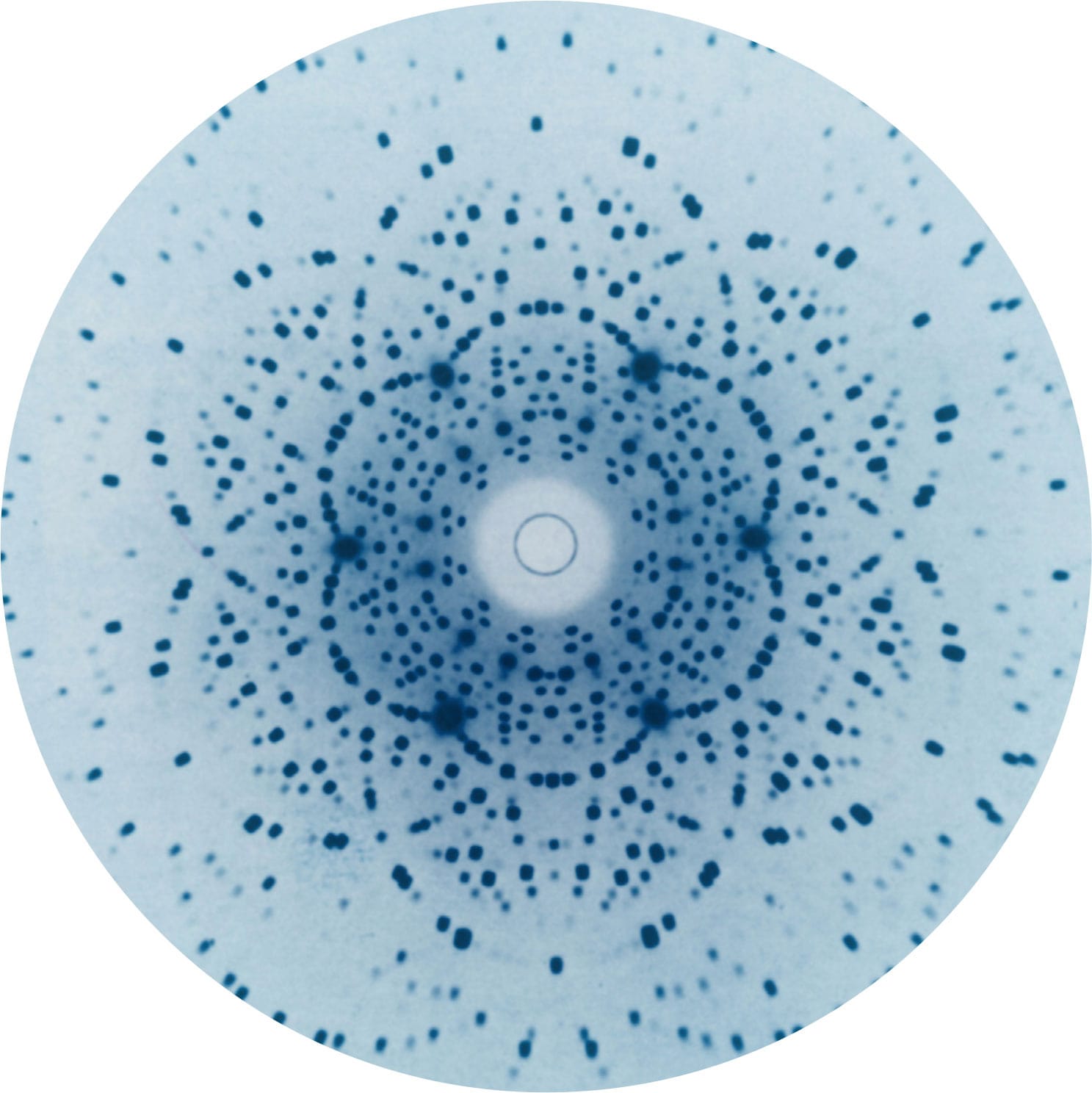
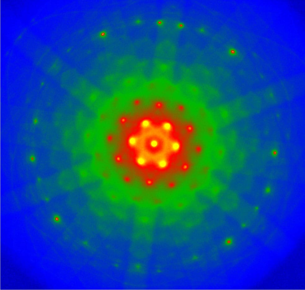
X-rays have a much shorter wavelength—from 100 Å down to 10 Å. This is close to the atomic scale and should certainly be able to resolve large molecules—in theory. However, there is no lens that can focus X-rays in the same way as light, so it is not practical to build an X-ray microscope to produce images of molecules. Furthermore, X-rays pass through most atoms instead of bouncing off. However, X-rays do diffract strongly as they pass through a substance. Diffraction is the bending of waves as they move past an edge or pass through a gap (see here); it is most noticeable when the gap is of comparable size to the wavelength.
The diffraction of X-rays through a regular array of atoms (or ions), as in a crystal, gives rise to regular patterns on a screen or a photographic plate. Beginning in the 1910s, X-ray crystallography has made it possible to work out the structure of crystals and molecules. But those wanting to produce images of actual atoms would have to wait for new techniques and technological advances.

Pass X-rays through a thin slice of aquamarine crystal (left) and the rays diffract strongly, because their wavelength is comparable to the atoms in the crystal. The diffracted rays interfere (see here), producing a pattern of dots that can be recorded on a photographic plate (above). The pattern, different for each compound, holds information about the positions of the atoms in the crystal (see here).
USING ELECTRONS
In the 1930s, a new type of microscope became available that uses electrons instead of light. As with all particles, electrons also behave as waves; their wavelengths depend upon their energy, and high-energy electrons can have wavelengths of around 1 picometer (pm): 0.01 Å. This makes them, in principle, easily able to resolve atoms. There are two main types of electron microscope: the scanning electron microscope (SEM) and the transmission electron microscope (TEM).
Inside an SEM, a beam of electrons scans across a prepared sample and a detector picks up the electrons that scatter off, building up a detailed image. The resolution of the image is limited by the width of the beam and the (electromagnetic) lenses that focus the beam and make it scan, but it can be as low as about 100 Å (10 nm). In a TEM, an electron beam passes through a thin sample, instead of bouncing off it. The resolution of a TEM depends upon the lenses as before, and also on the wavelength of the electrons—and that depends upon their energy, and therefore how fast they are accelerated to form the beam. This arrangement typically leads to a resolution of a few ångströms. From 1933, when the resolution of TEMs first surpassed the diffraction limit of optical microscopes, these microscopes provided biologists with ever more detailed views of the anatomy of biological cells and materials, giving scientists a better understanding of the structure of materials at the nanoscale.

Transmission electron micrograph of a mitochondrion—a structure in a cell that is a few hundred nanometers across. The folded membranes inside the mitochondrion, each a few nanometers thick, are easily resolved.
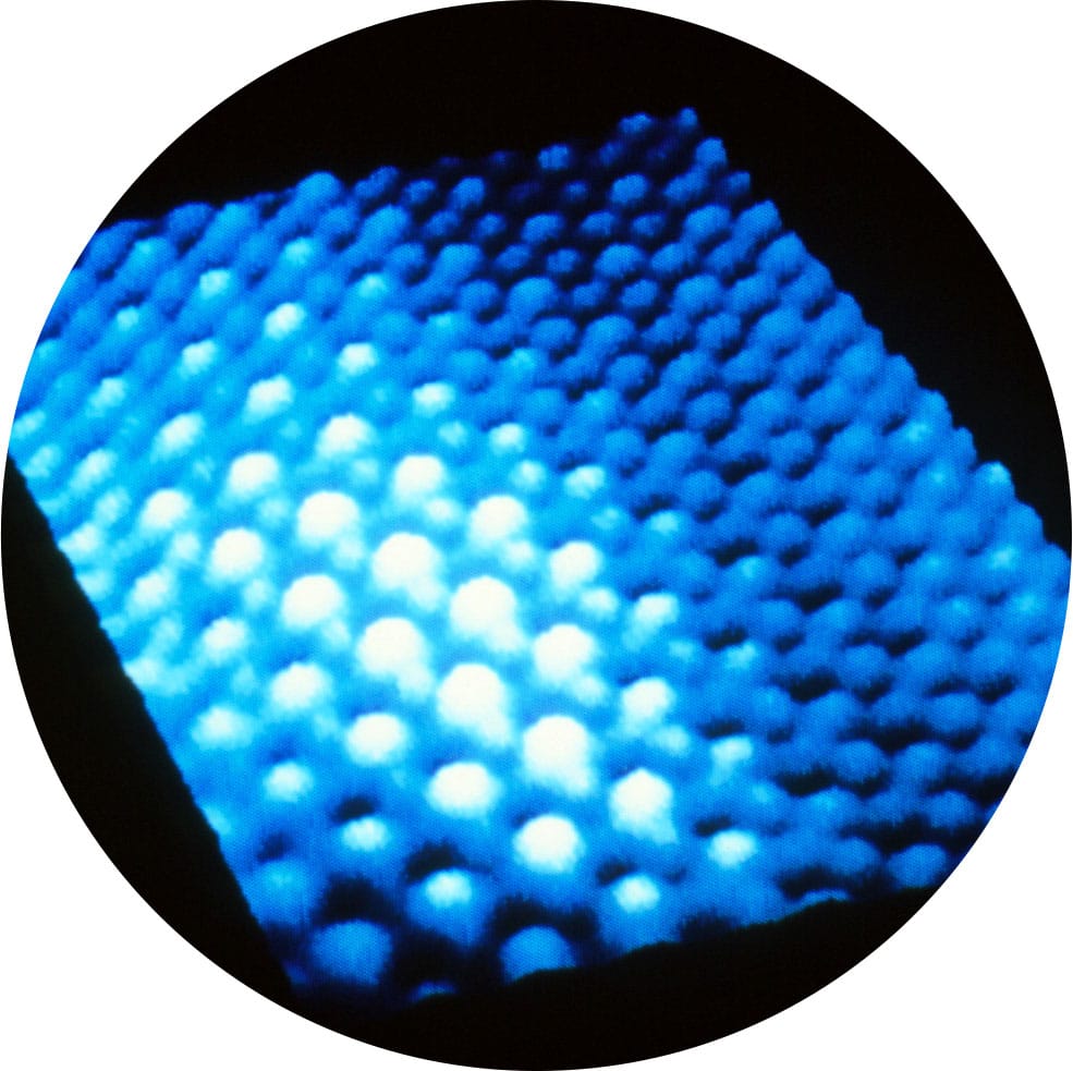
While electron microscopes were proving invaluable for biologists and materials scientists, they were still not able to produce images of atoms. A very different approach was needed to create the first such images. In 1936, German physicist Erwin Müller invented the field emission microscope (FEM), which produces images with a resolution close to the atomic scale. In an FEM, electrons are pushed away from a very sharp metal tip by a strong electric field. More electrons are released from areas, where the electron density is highest: around the atoms. The electrons follow the straight force lines of the electric field through a high vacuum. They end up on a detector where they form a projected image of the electron density at the surface of the metal tip.
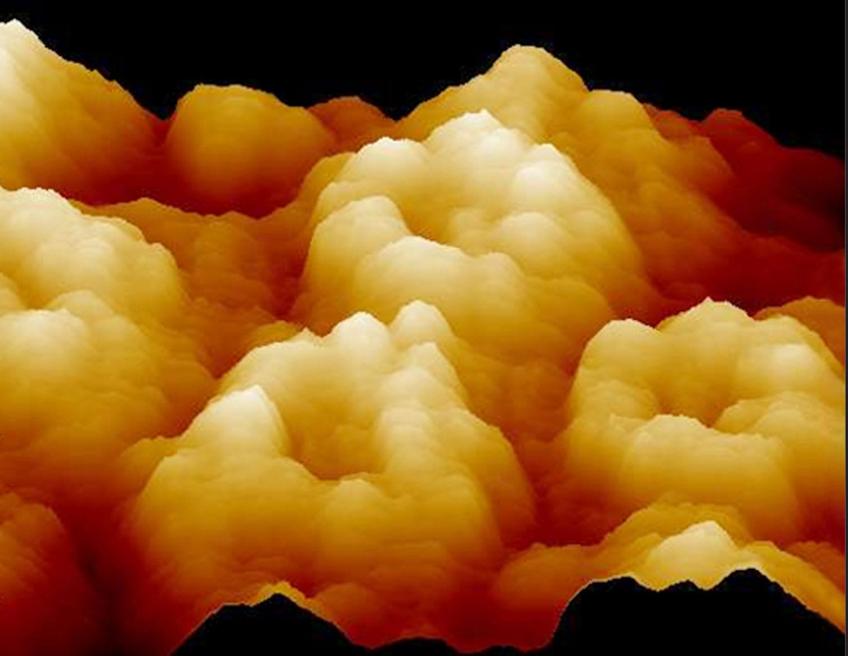
The blurry image of the atoms at the extremely sharp molybdenum tip of a field emission microscope.
In 1951, Müller made a crucial improvement to the device, introducing a small amount of gas, typically helium, into the apparatus. The result was the field ion microscope (FIM)—the first device to produce images of atoms. At very low temperatures, the helium atoms become adsorbed (stuck) to the atoms at the surface. When the electric field is then applied, the helium atoms become ionized and are pushed away from the metal tip. A screen detects the impacts of the helium ions, building up a picture of the atoms at the surface.
Field ion microscopy can produce images only of pure metals—and only those that can be made into extremely sharp tips. In the 1960s, Müller and his colleague John Panitz made a further improvement, allowing (ionized) atoms of the sample itself to fly away from the tip and onto the detector. With this “atom probe,” alloys (mixtures of metals) and even compounds can be analyzed. An important feature of the atom probe is a built-in mass spectrometer (see here) that measures the mass of the atoms received at the detector and can therefore identify which elements are present. Because the atoms peel away one layer at a time, the atom probe can produce a three-dimensional map of the internal structure of the tip, detailing the positions of atoms of different elements.

Atom probe microscopy can reveal the positions of atoms, and which element they belong to, in three dimensions. This image shows plate-shape precipitates and tiny spherical particles of tin in an aluminum alloy.
The first images of atoms were produced in 1955, by the inventor of the field ion microscope, Erwin Müller. Shown here is an image of the atoms on a platinum tip inside a field ion microscope.
FIELD ION MICROSCOPY

Atoms of an inert gas stick to the atoms at the surface of the sharp tip inside a field ion microscope. A high voltage on the tip ionizes the gas atoms, which then fly out directly to the phosphor screen.
SCANNING TRANSMISSION ELECTRON MICROSCOPE
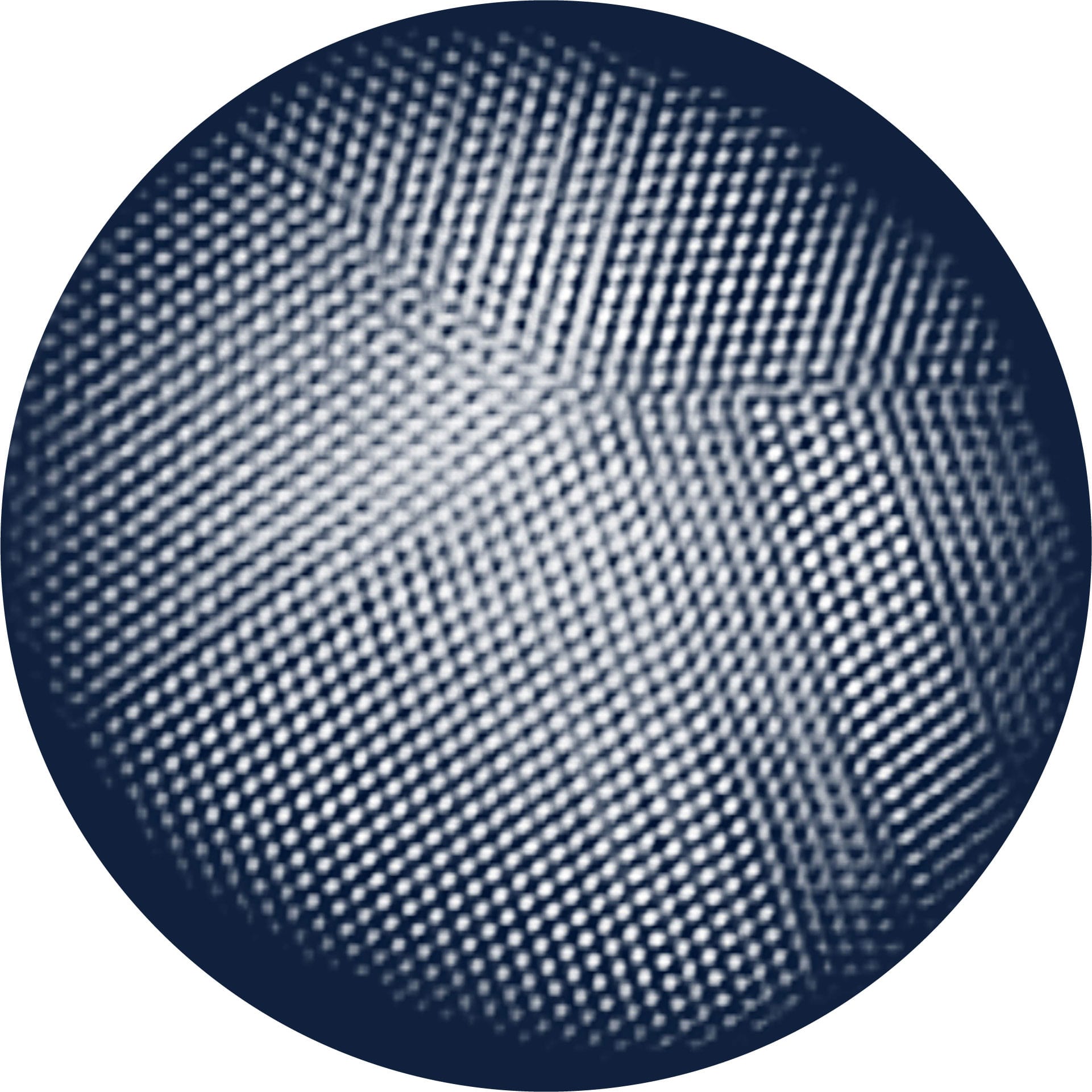
Adding to the growing array of technologies for producing images at or near atomic resolution—and to the list of acronyms they generate—is STEM: the scanning transmission electron microscope. Like transmission electron microscopy, STEM involves a beam of electrons passing through a thin sample of material. But in STEM, the beam is extremely narrow and is made to scan along successive lines, each one close to the last. This “raster scanning” maximizes the potential resolution of the electron beam and can produce clear images of atoms and atomic bonds. Additionally, detectors collect electrons that scatter off atoms in the sample at high angles, and also X-rays produced when the electron beam hits atoms and interatomic bonds. The energy (and therefore wavelength) of the X-rays depends upon the atomic number of the atom—so different elements can also be differentiated.
The image produced by electrons that have interacted with atoms within the sample and passed through is called the “light field image.” The electrons that are scattered to high angles away from the main path of the beam make up the “dark field image.” By combining both images and the information from the X-ray detector, STEM can reveal a wealth of information about the sample—and stunning, thought-provoking images.
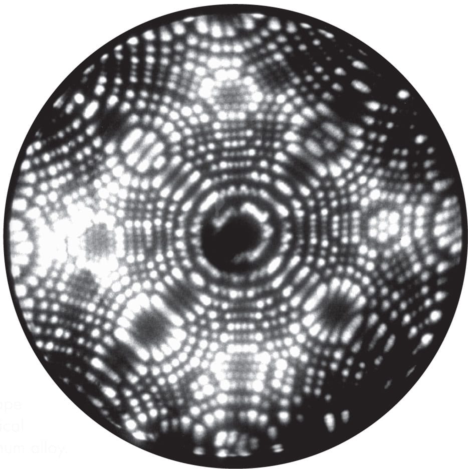
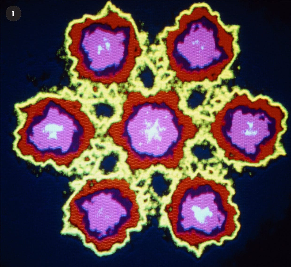
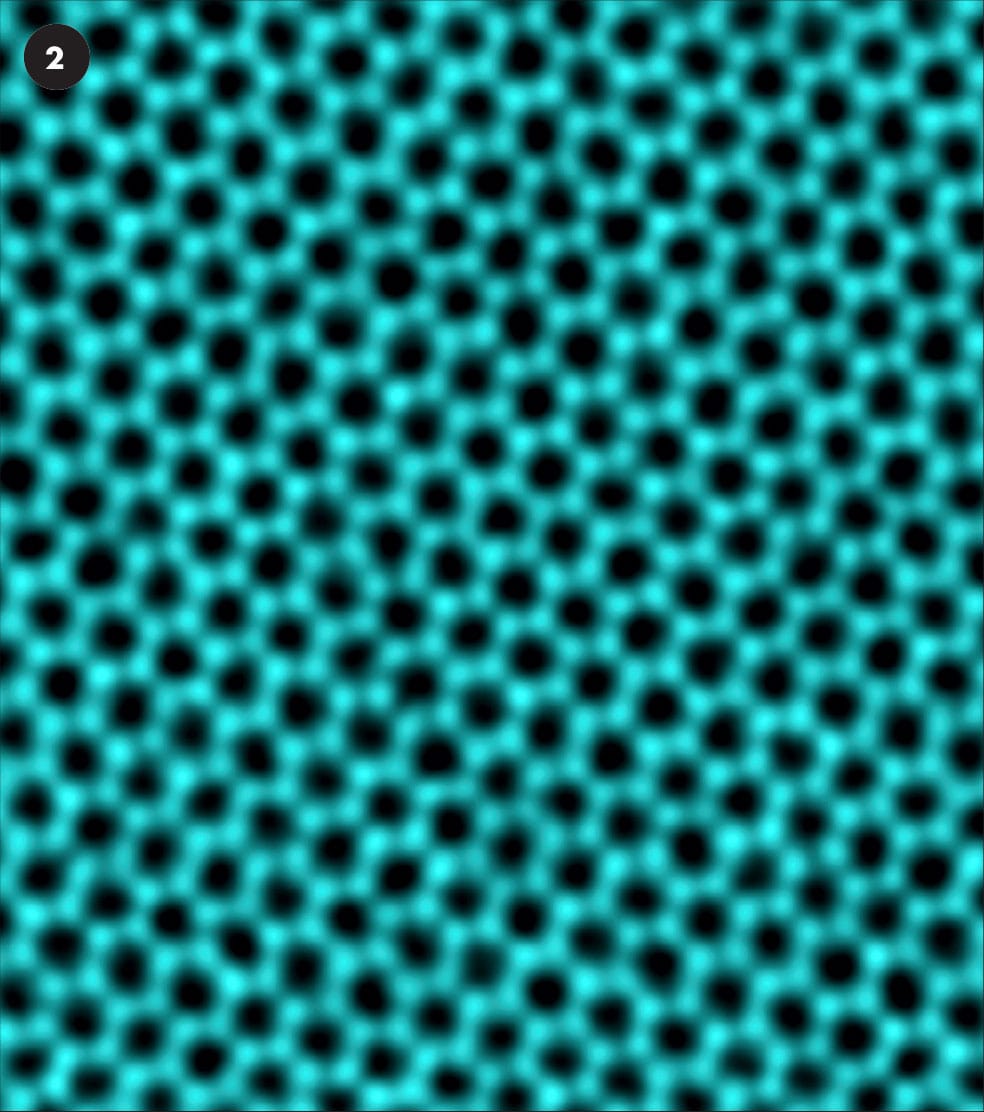
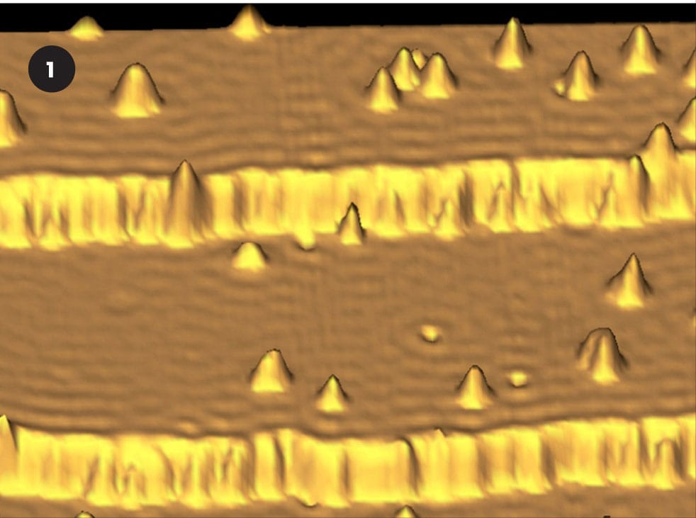
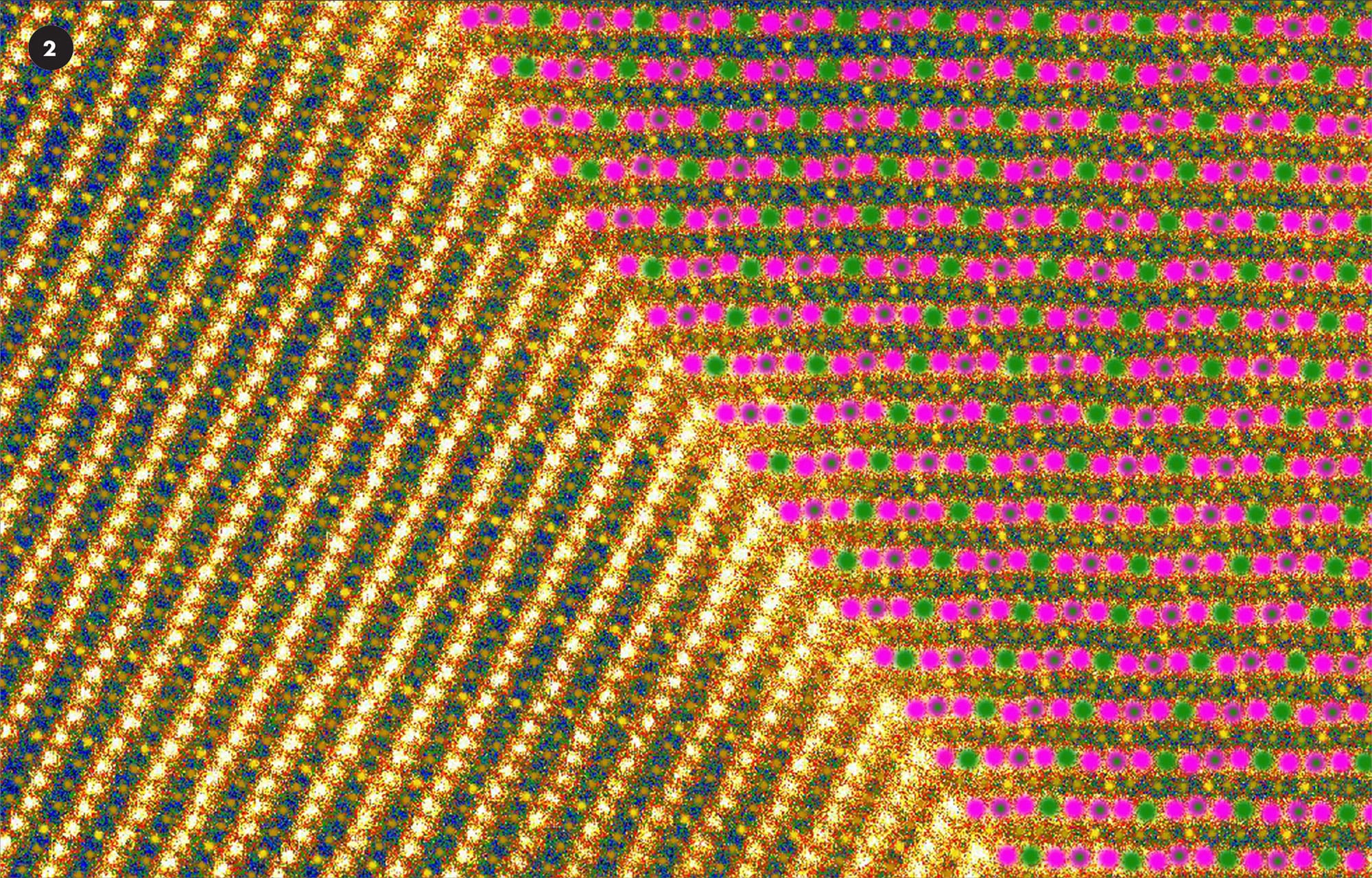
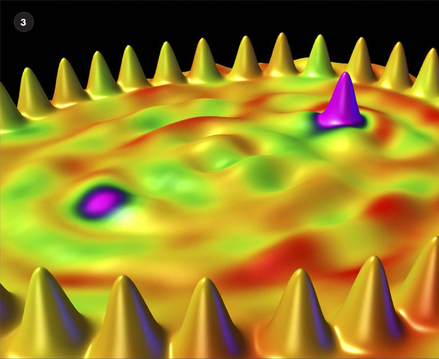
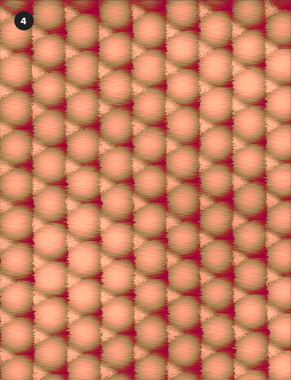
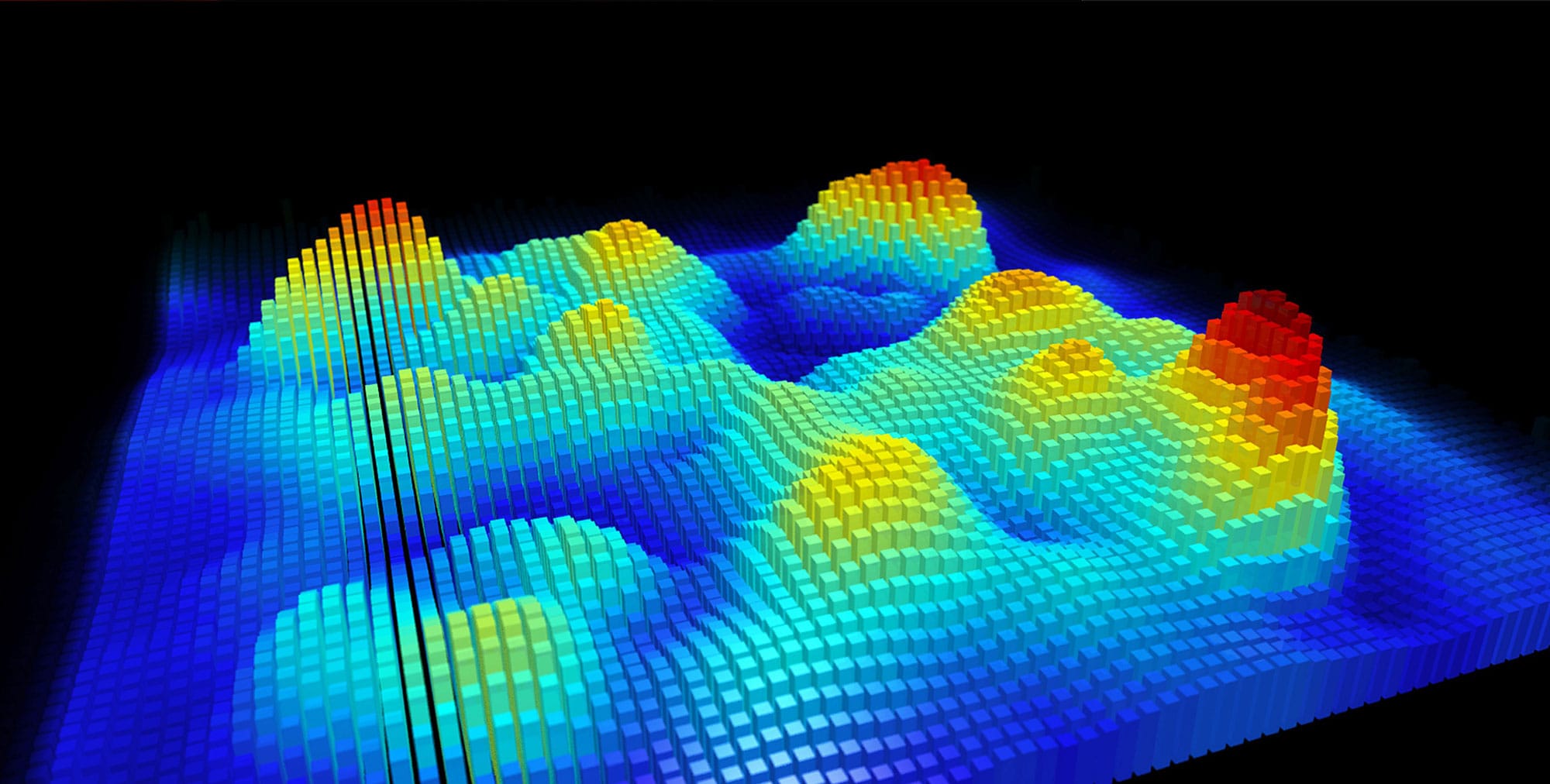
A selection of false-color STEM images.
1 Microcrystal of seven uranium atoms.
2 Graphene (see here)—each dot is a carbon atom, and the lines between them are covalent bonds.
3 An island of copper and silver atoms in a “sea” of aluminum atoms.
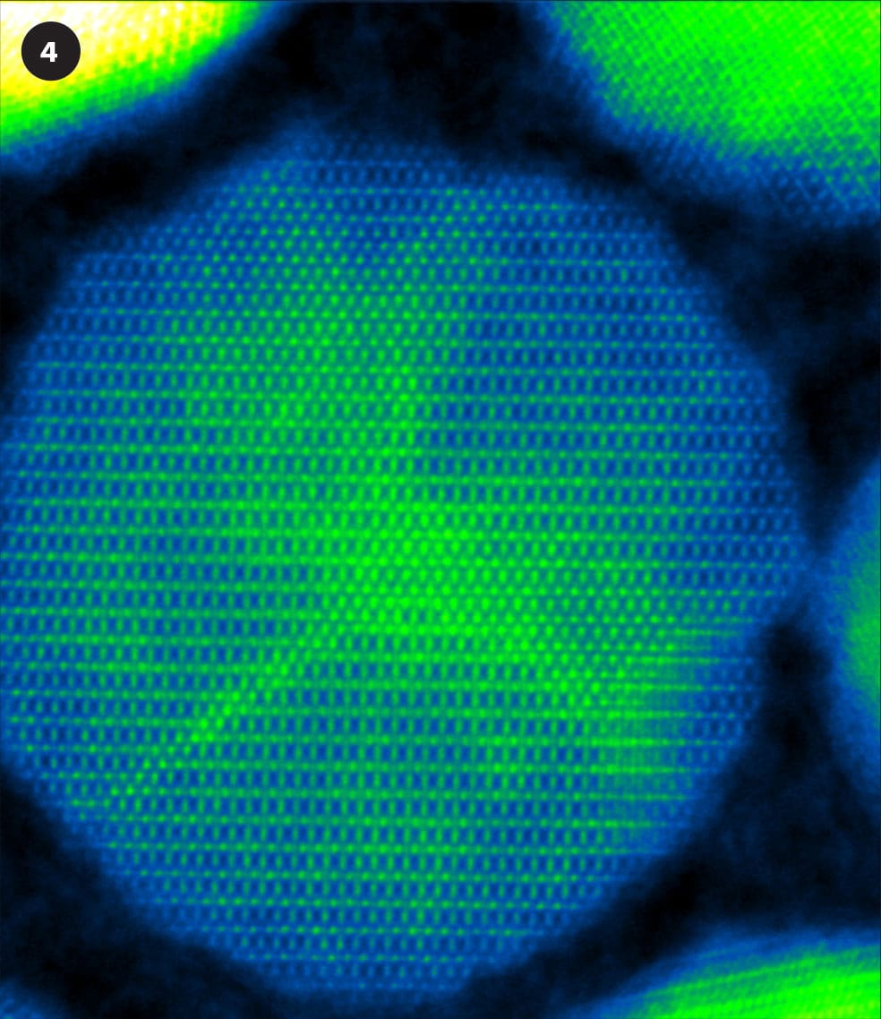
4 Nanoparticles of iron oxide.
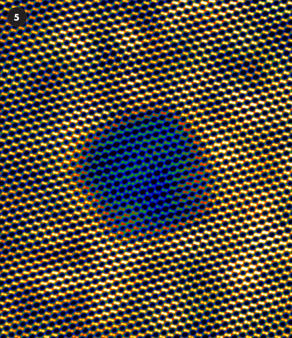
5 A tiny void less than 1 nanometer in diameter cut in a natural diamond (the orange dots are carbon atoms).
SCANNING PROBE MICROSCOPY
The best images of atoms to date have not been produced by X-rays or electron microscopes, nor by field ion microscopy or atom probes. Instead, they are the result of scanning the atomic-scale bumps in the surface of a sample with an extremely sharp probe. In addition to producing incredible images, some scanning probe microscopes can also interact directly with individual atoms and move them around.
SCANNING TUNNELING MICROSCOPE
The year 1981 brought a completely new way of producing faithful images of atoms at a surface, when Swiss physicist Heinrich Rohrer and German physicist Gerd Binnig invented the scanning tunneling microscope (STM). This remarkable device earned its inventors the 1986 Nobel Prize in Physics. The scanning tunneling microscope was the first of a new kind of imaging device: the scanning probe microscope. Instead of capturing an image of the surface directly by shining light, X-rays, or electron beams onto it, a scanning probe microscope builds up an accurate contour map of the surface by detecting the undulations of the surface in a series of scans. A little like reading braille, a scanning probe microscope builds up a picture of the shape of a surface by feeling its bumps.
The main feature of an STM is the probe that scans the surface. This is an extremely sharp metal point, only a few atoms wide at its tip, positioned a few ångströms above the surface of the sample. The sample itself needs to be a conductor, because the process depends upon a small electric current between the tip and the atoms at the surface. The voltage between the probe tip and the surface is not enough to generate a spark between them, even across such a tiny gap. Instead, electrons “leak” across the gap, one by one, by the quantum mechanical phenomenon of tunneling (see here). Specifically, the wave functions of the electrons at the surface extend above the surface, and the wave functions of the electrons in the tip extend beyond the tip, so that they overlap slightly (more so at very close separation or when the current is higher). This provides a small probability that electrons can tunnel across the gap. The greater the density of electrons at a particular point in the sample, and the closer the tip is to the surface, the greater that probability becomes—and the greater the tunneling current will be.
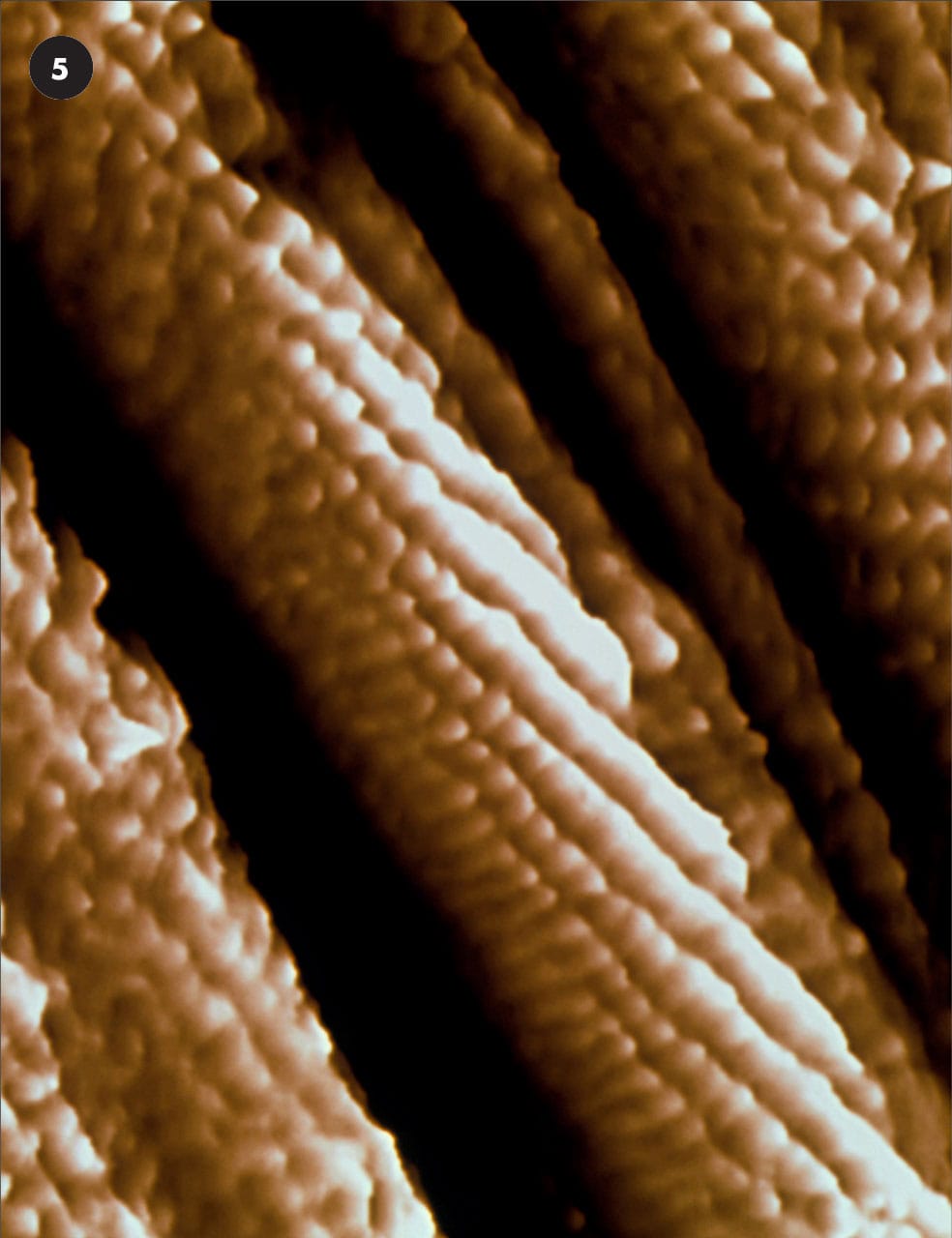
False color STM image of palladium atoms (white) on graphite (carbon atoms, blue). The palladium atoms are about 4 ångströms apart, the carbon atoms just over 3 ångströms apart.
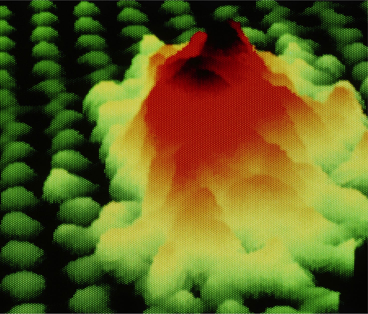
Early false color STM image from the 1980s—an intimate view of gold atoms (yellow, red, black) on a graphite surface (carbon atoms, green). The gold atoms have congregated into an island just greater than 1nanometer wide.
The probe scans along the surface in closely-spaced lines. The device detects the tunneling current and then automatically takes one of two actions. It either changes its height to maintain a constant tunneling current or maintains a constant height and measures the changes in tunneling current. In both cases, with scans along many adjacent lines, the device builds up a very accurate picture of the atom-size bumps in the surface. A computer puts the information together to produce a three-dimensional image.
STM image of individual manganese atoms (1) positioned on a gallium arsenide surface, as part of a research project that aims to increase the power and miniaturization of computer chips.
False color STM image of sodium atoms (2) (shown here yellow and dark green) and magnesium ions (pink and light green) in a manganese crystal.
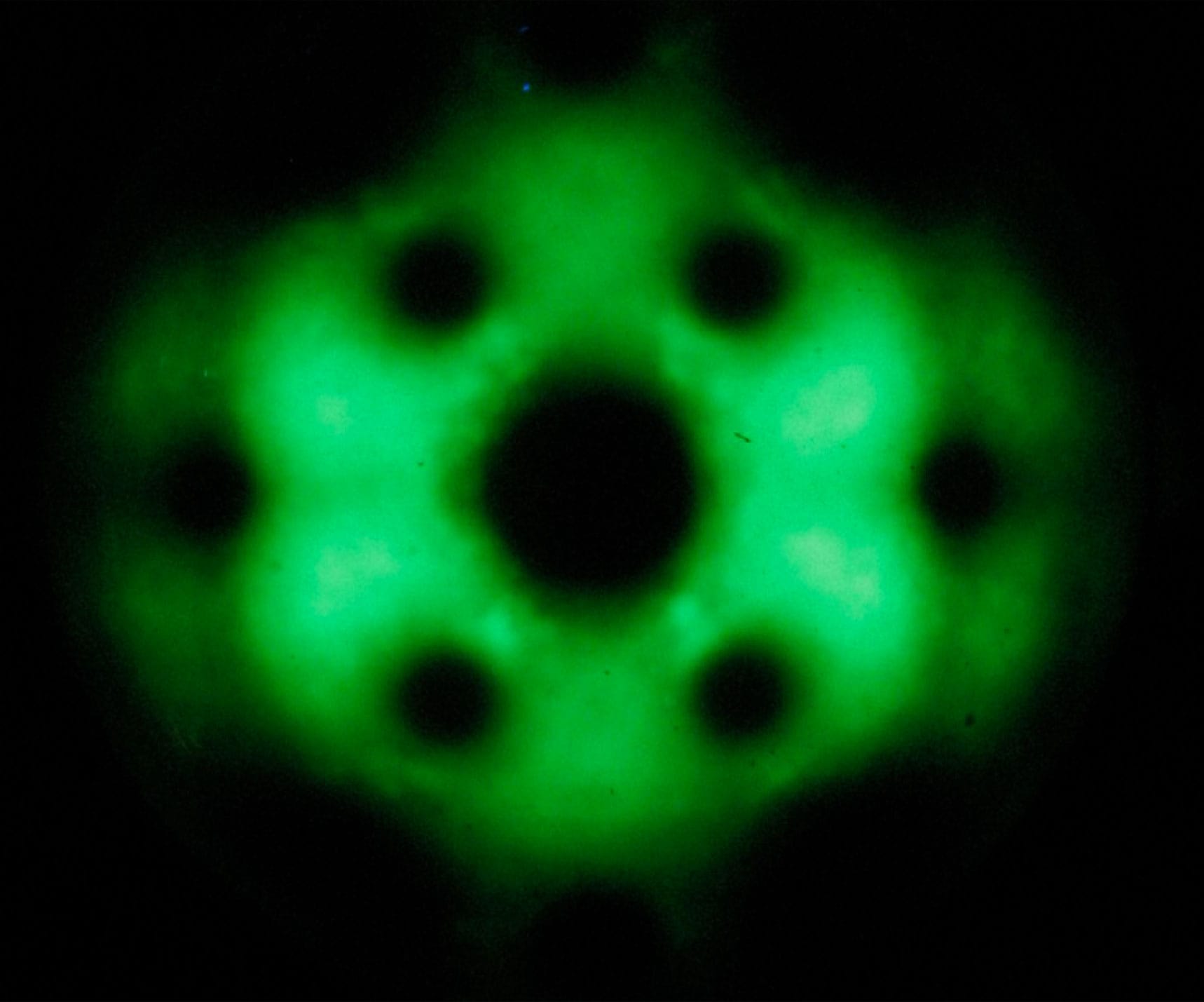
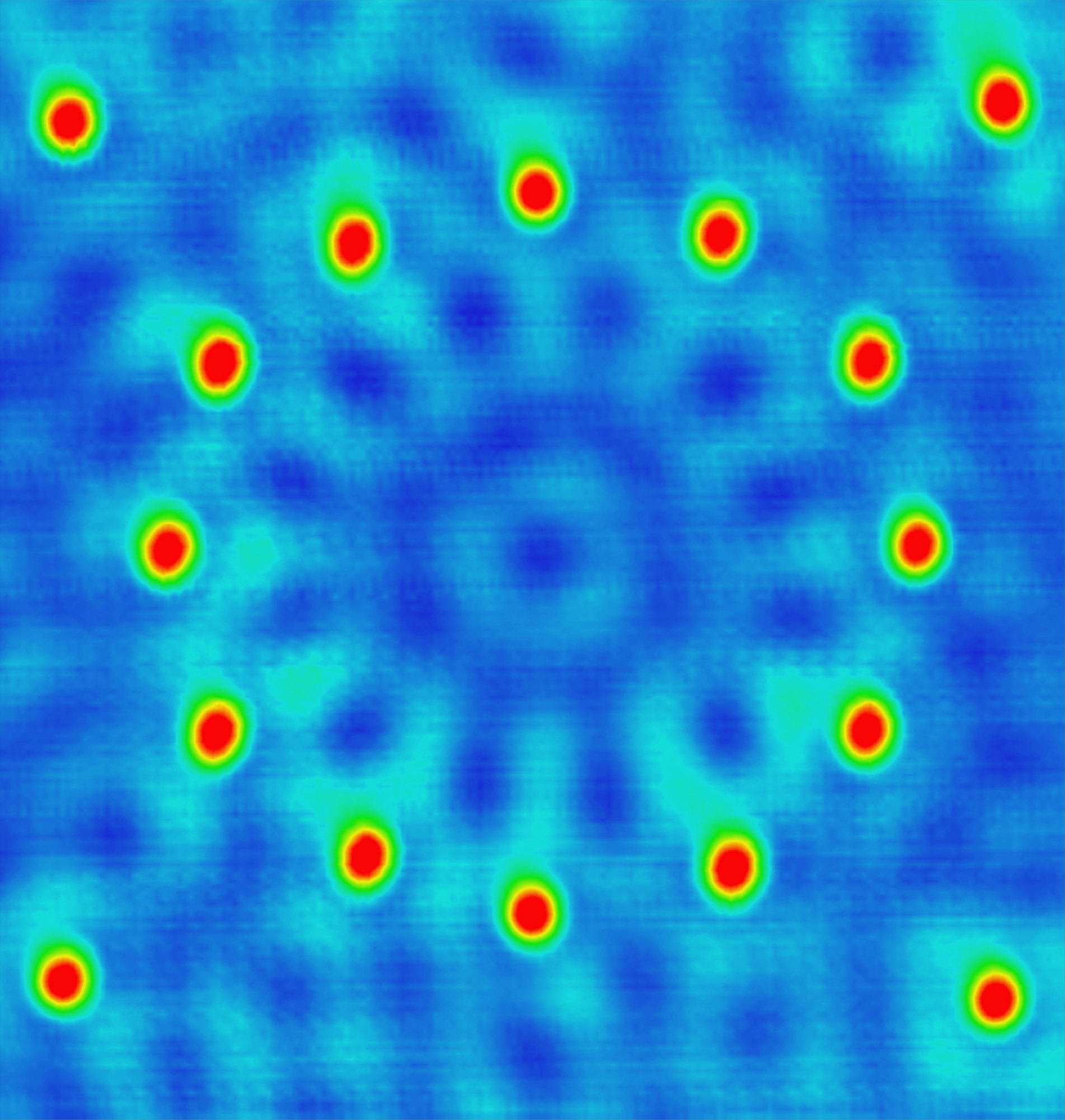
STM image of cobalt atoms (3) arranged in an elliptical structure known as a “corral”. Electron waves in the copper substrate interact with a magnetic coral atom (pink), resulting in a mirage effect: a phantom cobalt atom is visible at the other focus of the ellipse.
False color STM images showing (4) cobalt atoms (pink circles) on a copper surface, and (5) a stack of carbon nanotubes (see here).
ATOMIC FORCE MICROSCOPE
Amazing though it is, the STM has one key limitation: only conductive materials can be imaged, because the tunneling current that is key to its operation must be able to flow. That limitation was overcome in 1986—by the same team who invented the STM—with the invention of the atomic force microscope (AFM). The introduction of the AFM opened up scanning probe microscopy to a whole new array of materials. The principle behind the AFM is very similar to the STM, but instead of measuring a tunneling current, the instrument senses a tiny attractive or repulsive force between probe tip and surface atoms (see box below). The force is attractive at small distances, so the tip is normally positioned far enough away to make the force repulsive, avoiding the problem of the tip “sticking” to the surface.
The probe tip is attached to a flexible cantilever, and because the force varies with the atom-size bumps, the cantilever flexes up and down. The tiny movements of the cantilever are detected by bouncing a laser beam off it and onto a detector. Scanning across the surface in closely-spaced lines as before produces an atomic-scale image on a computer screen. In a variation of AFM, the probe tip is made to oscillate up and down at high frequency, but it does not make contact with the atoms at the surface. In this dynamic, or noncontact, mode, the frequency or the amplitude of the oscillations changes as the surface to tip force varies. With incredibly accurate measurements of the force between the surface atoms and the tip, atomic force microscopy can even identify the elements to which the atoms at the surface belong, atom by atom.
False color AFM image of pores in the membrane of a cell nucleus. A scanning tunneling microscope would not be able to produce this image, because the protein molecules that form the pore are not good conductors.
False color AFM image of a single molecule of naphthalocyanine, part of IBM’s research into single-molecule logic switches for future computer chips.
INTERACTING WITH ATOMS
Scanning probe microscopes can do more than produce incredible images of atoms: they can manipulate individual chemical bonds, triggering chemical reactions. Atomic physicists have developed many other ways to interact directly with atoms and molecules, utilizing knowledge of quantum mechanics to probe chemical reactions in real time and in exquisite detail, and even to create new forms of matter. They have also developed ways to investigate the incredibly rapid changes that take place during chemical reactions.
MOVING ATOMS
As if producing stunning, informative images and identifying the chemical elements present on a surface was not enough, scanning probe microscopes can interact directly with individual atoms. By adjusting the tunneling current of an STM and moving to just the correct distance from the surface, for example, the interaction between probe tip and the surface can be “tuned” to just the right level to form a chemical bond between an atom at the probe tip and an atom at the surface (typically, an “adatom”: one that has adhered to the surface, or been adsorbed onto it). The bond is strong enough to lift the atom away from the surface and move it, so that it can be deposited at another point.
This remarkable achievement allows for detailed studies of interatomic interactions in the real world—interactions that could previously only be studied mathematically, using quantum theory. But it may also enable nanoscale engineers to build minuscule electronic devices, such as computer memory or quantum dots (see here), consisting of just a few atoms, or to fabricate new materials with previously impossible properties. The daunting task of manufacturing such materials atom by atom may be diminished in the future by automating the process. In 2015, researchers at the U.S. National Institute of Standards and Technology (NIST) demonstrated a computer-controlled STM that moved cobalt atoms, strewn randomly on a copper surface, to form a quantum corral (see here). They also made quantum dots from carbon monoxide molecules and replicated the NIST logo at the nanoscale—all without human intervention.

False color STM image of a nanoscale abacus (left). The blue “beads” are buckminsterfullerene molecules (C60, see here) and the “frame” is a surface of copper. The STM probe tip was used to pick up and move the beads, one at a time. The false color STM image (facing page) is of cobalt atoms arranged in a circle on a copper surface.
TRIGGERING CHEMICAL REACTIONS
Another remarkable atomic interaction, made possible by a combination of AFM and STM, involved a chemical reaction called a Bergman cyclization (shown on the facing page). The reaction was discovered in 1972 and was initially considered as just a curiosity. But it now shows promise in developing anticancer drugs, because one of the intermediate molecules in the reaction can cleave DNA molecules, making it possible to destroy cancer cells in a targeted way. Researchers at IBM used scanning probe microscopy to study the reaction, and even to make it happen to order. They started by removing some atoms from a single molecule, leaving a stable molecule with three consecutive rings of carbon atoms. They then opened up the central ring, first on one side and then on the other, to make one of two different molecules—by breaking and making bonds between the carbon atoms with a tunneling current, as in STM. The system is a kind of molecular switch that could also one day be used in electronics, the two states of the molecule representing the binary “0” and “1” involved in digital systems.
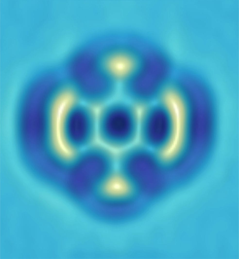
False color AFM image (top) of a single molecule of 9,10-dibromoanthracene on a two-atom-thick layer of sodium chloride. The two bromine atoms are at the top and bottom of the picture. To make this molecule into a molecular switch, IBM researchers first removed the bromine atoms with an STM probe.
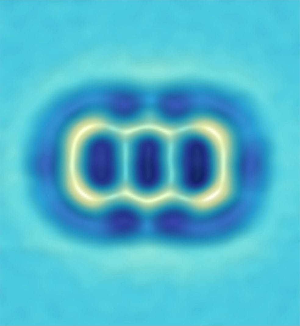
False color AFM image (bottom) of the single molecule switch made by IBM researchers after removal of the bromine atoms. The molecule is 9,10-didehydroanthracene. An STM probe tip was then used to break bonds in the molecule, switching between two states (see box on facing page).
SLOWING DOWN ATOMS
Another way in which atomic physicists can interact directly with atoms is by using lasers and magnetic fields to slow their motion, typically using a device called a magneto-optical trap (see box below). This apparatus can reduce the speeds of a population of atoms dramatically to the extent that they are barely moving and so have almost no kinetic energy. Because the average kinetic energy of a population of particles is related directly to that population’s temperature (see here), slowing atoms down equates to reducing their temperature. A magneto-optical trap can cool a gas almost to the lowest possible temperature:—to −459.67°F (−273.15°C), called “absolute zero.” This temperature equates precisely to zero on a specially conceived temperature scale called the Kelvin scale (K). One degree kelvin (1 K) is equal to 1.8°F (1°C), but the Kelvin scale’s zero is absolute zero. By interacting with atoms directly, physicists have managed to cool matter down to within one ten-billionth of a degree kelvin of absolute zero. (Note that it is not possible to have zero kinetic energy, because of “quantum fluctuations.” These are discussed in chapter seven.)

An actual magneto-optical trap at the Institute of Photonics and Advanced Sensing, University of Adelaide, Australia.
The ability to bring temperatures to within fractions of a degree of absolute zero has spawned many insightful research projects into atomic physics and materials science. Most notable among them is the creation of a strange form of matter called a Bose-Einstein condensate (BEC). The potential existence of BECs was first predicted in the 1920s by Albert Einstein and Indian physicist Satyendra Nath Bose. A BEC was created for the first time in 1995 by physicists at the University of Colorado.
In a BEC, all the atoms lose their individual identities and merge into one superparticle. This is because at extremely low temperatures, quantum effects become more prevalent, and atoms behave more like waves than particles; in a BEC, they are all defined by the same wave function (see here). At normal temperatures, atoms move around at a wide range of different speeds, and therefore there is a large distribution of different energies. Each atom has a different quantum state (a quantum state is a particle’s collection of “observables,” such as speed, position, and energy). As the temperature drops to close to absolute zero, the distribution of energies becomes far more restricted—and the quantization of energy comes into play (see here). Only certain energies are allowed, and as the atoms lose energy, they “fall” into, and occupy, all the available lowest-energy states—just as electrons fall into the lowest-energy state available in an atom.
In an atom, no two electrons can have precisely the same quantum state; they fill from the lowest-energy state. This behavior is characteristic of a class of particles called “fermions” (discussed further in chapter seven). Electrons, protons, and neutrons are all fermions, but not all particles are. Some are “bosons,” any number of which can occupy exactly the same energy state at the same time. Despite the fact that all atoms contain electrons, protons, and neutrons, some atoms as a whole are bosons. It is those bosonic atoms that can be coaxed into assuming the form of a BEC.
In order to create a BEC, experimenters inject a gas of (bosonic) atoms, normally rubidium or sodium, into the chamber of a magneto-optical trap that has had the air evacuated from it beforehand. The magneto-optical trap cools the gas to a few thousandths of a degree kelvin above absolute zero. The experimenters then irradiate the very cold gas with radio waves, which knocks the fastest-moving atoms away. This evaporative cooling (see here) removes only the most energetic atoms, reducing the cloud’s average kinetic energy significantly—enough for the temperature to drop to within a few millionths of a degree above absolute zero. Despite the very low temperature, the gas atoms neither condense to form a liquid nor freeze to form a solid, because the gas is rarefied; there are far fewer atoms per cubic centimeter than there are in air, let alone in a solid. Even as the atoms are squashed into a small space at the center of the chamber, they become a BEC before they have a chance to form a liquid or a solid.
FEMTOCHEMISTRY AND ATTOCHEMISTRY
The interactions between lasers and atoms have also allowed atomic physicists and chemists to investigate chemical reactions in unprecedented detail. The breaking and making of bonds that constitute chemical reactions (see here) occur very quickly—on timescales of femtoseconds (million-billionths of a second) and attoseconds (billion-billionths of a second). There are about as many attoseconds in one second as there have been seconds in the entire lifetime of the universe, so an attosecond is an extremely brief period of time.
The technology for investigating chemical reactions using lasers was developed in the 1990s by Egyptian-American chemist Ahmed Zewail. He was awarded the Nobel Prize for Chemistry in 1999 for his contributions. The main requirement is that the pulses of laser light used must be as short as possible—just as a camera shutter needs to remain open for as brief a period as possible if the camera is to capture a very fast-moving subject without blurring. This extreme resolution in the temporal (time) dimension is akin to the extreme resolution in the spatial dimensions achieved by scanning probe microscopes and scanning transmission electron microscopes; it presents another way to examine atomic-scale processes in intimate detail. Early femtosecond research, carried out by Zewail and his colleagues, involved first triggering a chemical reaction with a very short laser pulse. They then probed the state of the atoms and molecules taking part in the reaction at very short times afterward, using another short laser pulse. This “pulse-probe” approach is still the basis for investigating reactions on extremely short timescales, but there are now many variations on the theme. Several laboratories have also broken through the femtosecond barrier and are now working with pulses of laser light only attoseconds long.

Computer-generated simulation of the wave functions of cold, confined atoms as they begin to merge to form a Bose-Einstein condensate.
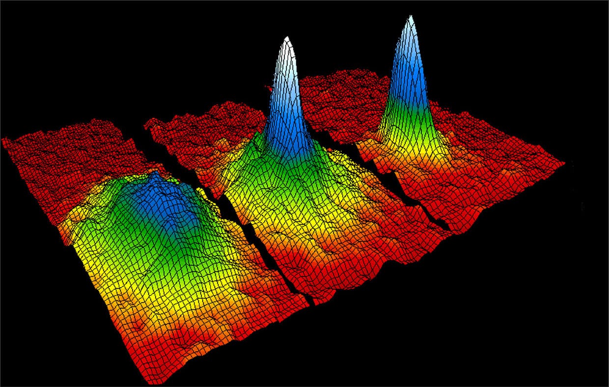
Graph showing the formation of the first Bose-Einstein condensate in 1995. The colors represent the density of rubidium atoms inside the magneto-optical trap. Red represents lowest density. White shows where the atoms have coalesced so that they share a single wave function.
Before ultrashort laser pulses were available, chemists could only work out how a reaction proceeds from scrutinizing the products—just as crash-scene investigators can only piece together what happened in an automobile accident by examining the wreckage. Femtochemistry and attochemistry provide the opportunity to construct an animation of the reaction in progress—similar to watching a crash over and over in slow motion. Every chemical reaction has an intermediate stage, between reactants and products, in which interatomic bonds have broken but new ones have not yet been made. The intermediate products of a reaction typically only last femtoseconds, or even attoseconds. The main driver of the development of extremely short timescale research is understanding in greater detail the dynamics of how these intermediates form and interact. In pulse-probe femto- and attosecond research, the first laser pulse knocks electrons to higher-energy levels, or provides enough energy to break the interatomic bonds of the reacting molecules. The second pulse interrogates the intermediate products. Typically, the researchers ascertain which bonds have been broken, and which electrons are at what levels, by observing which frequencies of light the molecules absorb—so this is a form of spectroscopy (see here). The researchers vary the interval between pulse and probe, enabling them to build up a picture of how the reaction proceeds from one tiny moment to the next.
The range of technologies available to short timescale researchers is expanding, and the basic pulse-probe approach is no longer the only way to interrogate rapid changes in molecules over very short timescales. Many researchers now use “free electron lasers” (see here), which can be tuned to produce powerful beams of electromagnetic radiation across a huge range of frequencies, from radio waves to X-rays. For probing reaction intermediates and products, many researchers employ electron diffraction. In this process, incoming radiation knocks electrons out of their bonds of a molecule; the electrons are then diffracted (see here) by the atoms present, and produce interference fringes on a screen. Such ultrafast electron diffraction can help researchers discern the positions of atoms in the intermediate molecules of a reaction to within less than an ångström.
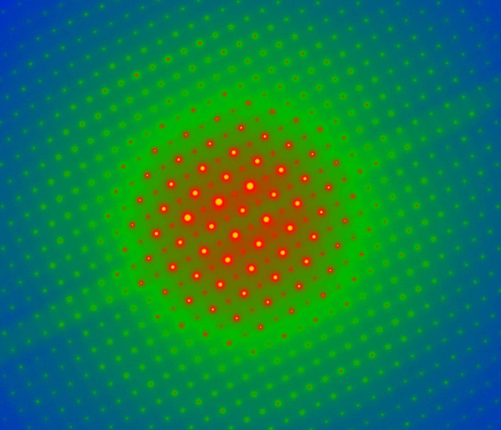
False-colored electron micrographs showing the electron diffraction pattern (see here) of pure silicon (top) and molybdenum trioxide (bottom). In ultrafast electron diffraction, incoming electrons disturb the crystal, changing the structure momentarily and revealing information about the bonds between the atoms.
FEMTOSECOND SPECTROSCOPY
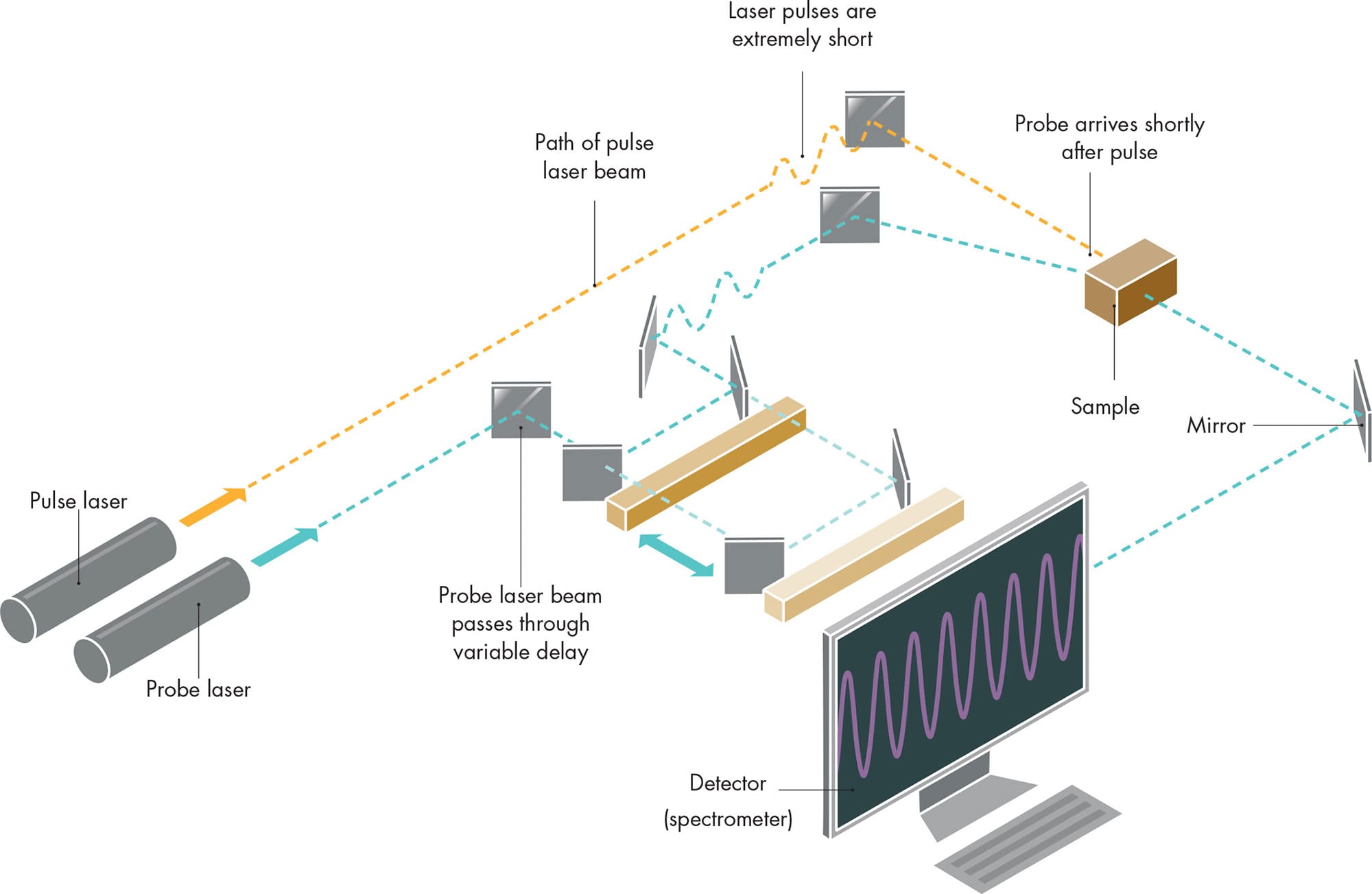
Typical laboratory setup for femtosecond research. The time delay between pulse and probe is varied by moving the mirrors back and forth in the optical path of the probe beam, so that the probe takes less or more time to reach the sample.
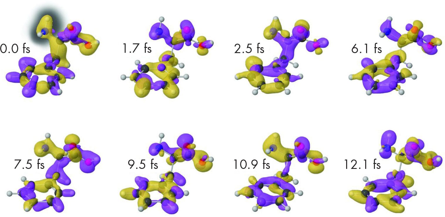
The results of femtosecond spectroscopy reveal extremely rapid changes in molecules. Here, the technique tracks the shifting molecular orbitals in a molecule of phenylalanine after it is hit by a laser pulse. The entire sequence lasts just 12 femtoseconds (fs) or 12 million billionths of a second.