A Raspberry Pi Expansion Board
In this chapter, we will look in detail at another of the author’s open-source hardware (OSH) projects, specifically, version two of the RaspiRobot board (www.raspirobot.com). This board (Figure 9-1) is designed to allow a Raspberry Pi single-board computer to be powered by batteries and also to control two direct-current (dc) motors. The board has a number of interfaces including to an HC-SR-04 ultrasonic range finder, a 5V I2C interface designed to easily accommodate displays and other I2C devices, and a pair of open-collector outputs.
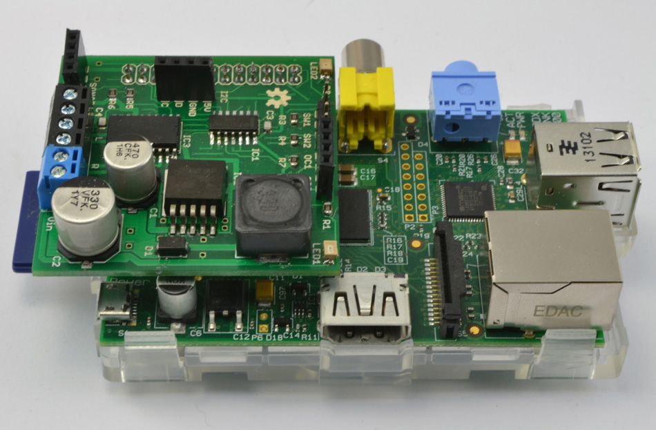
FIGURE 9-1 The RaspiRobot board version 2.
In following this design, you will learn how to develop your own add-on boards for the Raspberry Pi.
![]()
The board is interesting from a design point of view because it uses a switched-mode power-supply chip that has very specific routing requirements. The board also uses a mixture of both through-hole and surface-mount devices. Figure 9-2 shows a block diagram for the design.
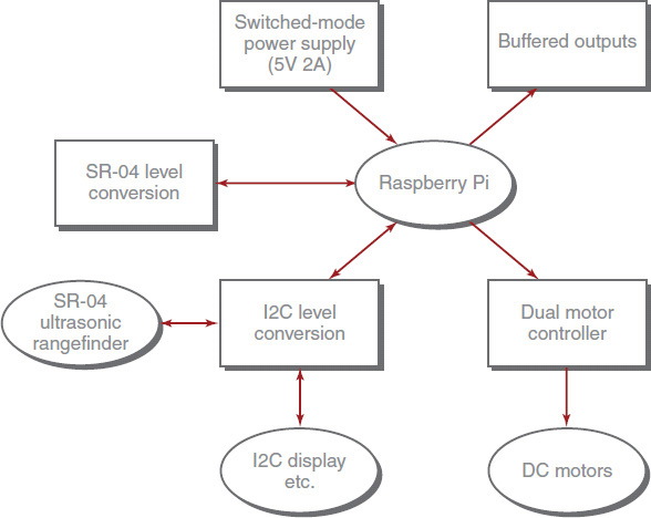
FIGURE 9-2 Block diagram for the RaspiRobot board.
The round objects are external to the RaspiRobot board, and the rectangular blocks are part of the board. This type of diagram can be very useful for setting the context of the project and understanding how it will interface with other parts of the system.
![]()
There is nothing particularly interesting about the schematic (Figure 9-3), so we will not dwell on it for long.
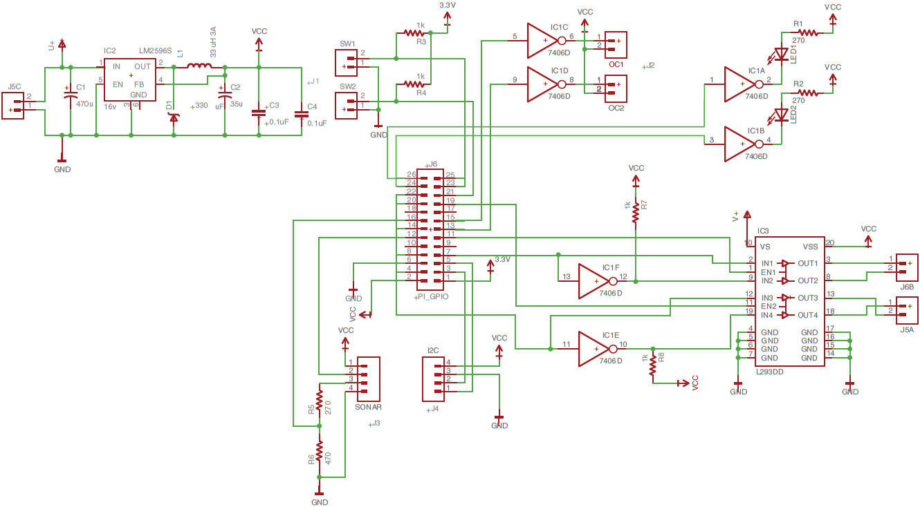
FIGURE 9-3 Final schematic.
One quite common pattern in the schematic design is worth mentioning, and that is the separating out of the power-supply section of the board. This has the components for the power supply itself and the decoupling capacitors (C3 and C4) on their own. Separating the power-supply section of the board like this is a lot clearer than adding nets as lines between all the components.
The Raspberry Pi, to which the board will be attached, is represented in the schematic as a 2- by 13-in. socket header.
![]()
The board was designed using a mixture of manual and automated layout. Figure 9-4 shows the initial placement of the components.

FIGURE 9-4 Initial component placement.
In considering the board design, there are two areas where it is worth some manual layout before we unleash the autorouter. These are
• The critical layout considerations for the power-supply chip IC2 and its associated components
• The power supply and outputs of the motor controller chip IC3
As you can see, the power-supply components take almost a third of the right-hand side of the board. The switched-mode power supply is based around the LM2596S chip. The datasheet for this integrated circuit (IC) indicates that there are certain paths between its associated components that need to be as short and low resistance as possible; otherwise, instability will result. There are also some fairly large currents flowing here. Figure 9-5 shows the relevant part of the datasheet indicating the paths that need to be kept as short as possible.
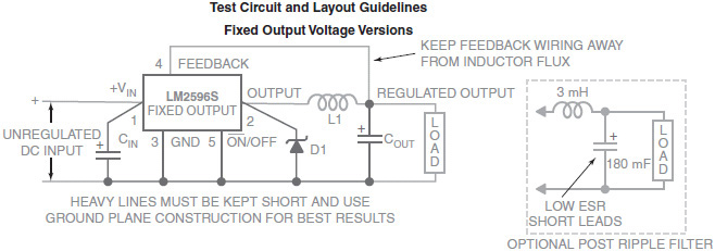
FIGURE 9-5 Critical connections on the LM2596S.
As the note in the datasheet states, a ground-plane construction is ideal, and we will use this for much of the power-supply area, with some short and thick tracks for the areas not connected by the ground plane.
We will use a ground plane over the whole bottom layer and a second ground plane around IC2 D1, C1, and C2. The inductor does not have a connection to GND because it will be connected to pins of IC2, which must be on the top layer; thus there is little point in extending the ground plane up to L1. Figure 9-6 shows the board with the two ground planes added. Note how I have added a grid of vias to link the two ground planes.

FIGURE 9-6 Adding ground planes.
This figure indicates that the connections between L1 and IC2 are not critical, but common sense dictates that these tracks will be carrying significant current, so let’s start by routing them with some fairly thick tracks (40 mils). The connection between L1 and D1 is also marked as critical, so let’s do the same for that connection. This last net also connects to pin 2 of IC2. This is handily close to D1, but if we used 40 mils, we would be getting close to neighboring pins of IC2, so for this short track the width was dropped to 32 mils.
While we are dealing with the high-current tracks, let’s also add in the track between Vin, C1, and pin 1 of IC2. Again, let’s make these in 40-mil width. Remember to keep clicking the Ratsnest command when routing through the top ground plane. The result of these routings is shown in Figure 9-7.
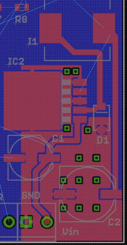
FIGURE 9-7 Routing the power supply.
Referring again to Figure 9-5, pin 4 of IC2 is a feedback signal. It measures the voltage being output. This will not be carrying any significant current, but the datasheet indicates that it should be kept away from the inductor. This track can just travel out horizontally from pin 4 of IC2. It does not need to be thick, but it does need to get past the track on the top layer from C2 to L1. We can do this by hopping under it using a pair of vias.
When routing from one layer to another, do not place the vias first. They will be placed automatically for you as you switch layers. This is illustrated in Figure 9-8.
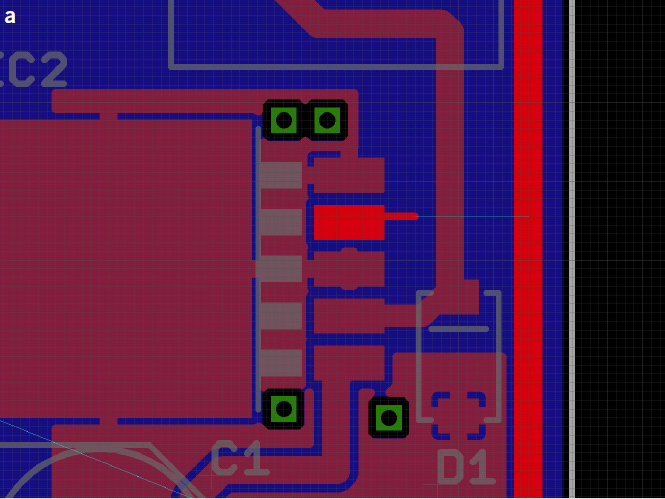


FIGURE 9-8 Routing across layers.
First, set the width to 10 mils, and start making the track from IC2 pin 4 on the top layer (Figure 9-8a). When you get halfway to the vertical track that we want to go under, left-click the mouse. This is where the via will go when we switch layers. Thus, without changing away from the Routing tool, move the mouse up to the layer dropdown and select the bottom layer. Move the track on a little further to the right. You will see that it is now routing on the bottom layer (Figure 9-8b). The via has not yet appeared, but it will soon.
Almost immediately we will need to swap layers again, so left-click the mouse where you want the via, and then select the top layer again. At this point, the first via will appear (Figure 9-8c). Finally, complete the track, routing it to the right-most vertical track, and both vias will be visible. Click on “Ratsnest” to make a gap around the track on the bottom layer so that it is not merged with the bottom ground plane (Figure 9-8d).
The other area of the board that is worth manually routing concerns the other high-current tracks, that is, the tracks from IC3 to the screw terminals that provide power to the motors and also the regulated 5-V line that provides power to the Raspberry Pi. Again, the width is chosen to be as wide as can be easily accommodated. In some places, this width is reduced midway along the track as it nears a pad. Figure 9-9 shows the final board with these air wires routed and the remainder of the board routed using the autorouter.

FIGURE 9-9 Final board layout.
![]()
In this second example chapter we have learned about routing with a mixture of manual routing and the autorouter. In Chapter 10, we will look at how you can interact with EAGLE using text commands and then extend this to automate what would otherwise be tedious and repetitive tasks using scripts and user-language programs (ULPs).