Chapter 3
CPUs
Chapter Points
• Input and output mechanisms.
• Supervisor mode, exceptions, and traps.
• Memory management and address translation.
3.1 Introduction
This chapter describes aspects of CPUs that do not directly relate to their instruction sets. We consider a number of mechanisms that are important to interfacing to other system elements, such as interrupts and memory management. We also take a first look at aspects of the CPU other than functionality—performance and power consumption are both very important attributes of programs that are only indirectly related to the instructions they use.
In Section 3.2, we study input and output mechanisms including both busy/wait and interrupts. Section 3.3 introduces several specialized mechanisms for operations like detecting internal errors and protecting CPU resources. Section 3.4 introduces co-processors that provide optional support for parts of the instruction set. Section 3.5 describes the CPU’s view of memory—both memory management and caches. The next sections look at nonfunctional attributes of execution: Section 3.6 looks at performance while Section 3.7 considers power consumption. Finally, in Section 3.8 we use a data compressor as an example of a simple yet interesting program.
3.2 Programming Input and Output
The basic techniques for I/O programming can be understood relatively independent of the instruction set. In this section, we cover the basics of I/O programming and place them in the contexts of the ARM, C55x, and PIC16F. We begin by discussing the basic characteristics of I/O devices so that we can understand the requirements they place on programs that communicate with them.
3.2.1 Input and Output Devices
Input and output devices usually have some analog or nonelectronic component—for instance, a disk drive has a rotating disk and analog read/write electronics. But the digital logic in the device that is most closely connected to the CPU very strongly resembles the logic you would expect in any computer system.
Figure 3.1 shows the structure of a typical I/O device and its relationship to the CPU. The interface between the CPU and the device’s internals (e.g., the rotating disk and read/write electronics in a disk drive) is a set of registers. The CPU talks to the device by reading and writing the registers. Devices typically have several registers:
• Data registers hold values that are treated as data by the device, such as the data read or written by a disk.
• Status registers provide information about the device’s operation, such as whether the current transaction has completed.
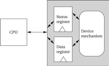
Figure 3.1 Structure of a typical I/O device.
Some registers may be read-only, such as a status register that indicates when the device is done, while others may be readable or writable.
Application Example 3.1 describes a classic I/O device.
Application Example 3.1 The 8251 UART
The 8251 UART (Universal Asynchronous Receiver/Transmitter) [Int82] is the original device used for serial communications, such as the serial port connections on PCs. The 8251 was introduced as a stand-alone integrated circuit for early microprocessors. Today, its functions are typically subsumed by a larger chip, but these more advanced devices still use the basic programming interface defined by the 8251.
The UART is programmable for a variety of transmission and reception parameters. However, the basic format of transmission is simple. Data are transmitted as streams of characters in this form:
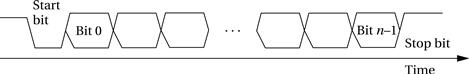
Every character starts with a start bit (a 0) and a stop bit (a 1). The start bit allows the receiver to recognize the start of a new character; the stop bit ensures that there will be a transition at the start of the stop bit. The data bits are sent as high and low voltages at a uniform rate. That rate is known as the baud rate; the period of one bit is the inverse of the baud rate.
Before transmitting or receiving data, the CPU must set the UART’s mode register to correspond to the data line’s characteristics. The parameters for the serial port are familiar from the parameters for a serial communications program:
• mode[1:0]: mode and baud rate
• 01: asynchronous mode, no clock prescaler
• 10: asynchronous mode, 16x prescaler
• 11: asynchronous mode, 64x prescaler
Setting bits in the command register tells the UART what to do:
The status register shows the state of the UART and transmission:
• status [0]: transmitter ready
• status [2]: transmission complete
The UART includes transmit and receive buffer registers. It also includes registers for synchronous mode characters.
The Transmitter Ready output indicates that the transmitter is ready to accept a data character; the Transmitter Empty signal goes high when the UART has no characters to send. On the receiver side, the Receiver Ready pin goes high when the UART has a character ready to be read by the CPU.
3.2.2 Input and Output Primitives
Microprocessors can provide programming support for input and output in two ways: I/O instructions and memory-mapped I/O. Some architectures, such as the Intel x86, provide special instructions (in and out in the case of the Intel x86) for input and output. These instructions provide a separate address space for I/O devices.
But the most common way to implement I/O is by memory mapping—even CPUs that provide I/O instructions can also implement memory-mapped I/O. As the name implies, memory-mapped I/O provides addresses for the registers in each I/O device. Programs use the CPU’s normal read and write instructions to communicate with the devices.
Example 3.1 illustrates memory-mapped I/O on the ARM.
Example 3.1 Memory-Mapped I/O on ARM
We can use the EQU pseudo-op to define a symbolic name for the memory location of our I/O device:
DEV1 EQU 0x1000
Given that name, we can use the following standard code to read and write the device register:
LDR r1,#DEV1 ; set up device address
LDR r0,[r1] ; read DEV1
LDR r0,#8 ; set up value to write
STR r0,[r1] ; write 8 to device
How can we directly write I/O devices in a high-level language like C? When we define and use a variable in C, the compiler hides the variable’s address from us. But we can use pointers to manipulate addresses of I/O devices. The traditional names for functions that read and write arbitrary memory locations are peek and poke. The peek function can be written in C as:
int peek(char *location) {
return *location; /* de-reference location pointer */
}
The argument to peek is a pointer that is de-referenced by the C * operator to read the location. Thus, to read a device register we can write:
#define DEV1 0x1000
…
dev_status = peek(DEV1); /* read device register */
The poke function can be implemented as:
void poke(char *location, char newval) {
(*location) = newval; /* write to location */
}
To write to the status register, we can use the following code:
poke(DEV1,8); /* write 8 to device register */
These functions can, of course, be used to read and write arbitrary memory locations, not just devices.
3.2.3 Busy-Wait I/O
The simplest way to communicate with devices in a program is busy-wait I/O. Devices are typically slower than the CPU and may require many cycles to complete an operation. If the CPU is performing multiple operations on a single device, such as writing several characters to an output device, then it must wait for one operation to complete before starting the next one. (If we try to start writing the second character before the device has finished with the first one, for example, the device will probably never print the first character.) Asking an I/O device whether it is finished by reading its status register is often called polling.
Example 3.2 illustrates busy-wait I/O.
Example 3.2 Busy-Wait I/O Programming
In this example we want to write a sequence of characters to an output device. The device has two registers: one for the character to be written and a status register. The status register’s value is 1 when the device is busy writing and 0 when the write transaction has completed.
We will use the peek and poke functions to write the busy-wait routine in C. First, we define symbolic names for the register addresses:
#define OUT_CHAR 0x1000 /* output device character register */
#define OUT_STATUS 0x1001 /* output device status register */
The sequence of characters is stored in a standard C string, which is terminated by a null (0) character. We can use peek and poke to send the characters and wait for each transaction to complete:
char *mystring = “Hello, world.” /* string to write */
char *current_char; /* pointer to current position in string */
current_char = mystring; /* point to head of string */
while (*current_char != ‘\0’) { /* until null character */
poke(OUT_CHAR,*current_char); /* send character to device */
while (peek(OUT_STATUS) != 0); /* keep checking status */
current_char++; /* update character pointer */
}
The outer while loop sends the characters one at a time. The inner while loop checks the device status—it implements the busy-wait function by repeatedly checking the device status until the status changes to 0.
Example 3.3 illustrates a combination of input and output.
Example 3.3 Copying Characters from Input to Output Using Busy-Wait I/O
We want to repeatedly read a character from the input device and write it to the output device. First, we need to define the addresses for the device registers:
#define IN_DATA 0x1000
#define IN_STATUS 0x1001
#define OUT_DATA 0x1100
#define OUT_STATUS 0x1101
The input device sets its status register to 1 when a new character has been read; we must set the status register back to 0 after the character has been read so that the device is ready to read another character. When writing, we must set the output status register to 1 to start writing and wait for it to return to 0. We can use peek and poke to repeatedly perform the read/write operation:
while (TRUE) { /* perform operation forever */
/* read a character into achar */
while (peek(IN_STATUS) == 0); /* wait until ready */
achar = (char)peek(IN_DATA); /* read the character */
/* write achar */
poke(OUT_DATA,achar);
poke(OUT_STATUS,1); /* turn on device */
while (peek(OUT_STATUS) != 0); /* wait until done */
}
3.2.4 Interrupts
Basics
Busy-wait I/O is extremely inefficient—the CPU does nothing but test the device status while the I/O transaction is in progress. In many cases, the CPU could do useful work in parallel with the I/O transaction:
• computation, as in determining the next output to send to the device or processing the last input received, and;
To allow parallelism, we need to introduce new mechanisms into the CPU.
The interrupt mechanism allows devices to signal the CPU and to force execution of a particular piece of code. When an interrupt occurs, the program counter’s value is changed to point to an interrupt handler routine (also commonly known as a device driver) that takes care of the device: writing the next data, reading data that have just become ready, and so on. The interrupt mechanism of course saves the value of the PC at the interruption so that the CPU can return to the program that was interrupted. Interrupts therefore allow the flow of control in the CPU to change easily between different contexts, such as a foreground computation and multiple I/O devices.
As shown in Figure 3.2, the interface between the CPU and I/O device includes several signals for interrupting:
• the I/O device asserts the interrupt request signal when it wants service from the CPU;
• the CPU asserts the interrupt acknowledge signal when it is ready to handle the I/O device’s request.
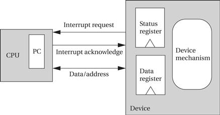
Figure 3.2 The interrupt mechanism.
The I/O device’s logic decides when to interrupt; for example, it may generate an interrupt when its status register goes into the ready state. The CPU may not be able to immediately service an interrupt request because it may be doing something else that must be finished first—for example, a program that talks to both a high-speed disk drive and a low-speed keyboard should be designed to finish a disk transaction before handling a keyboard interrupt. Only when the CPU decides to acknowledge the interrupt does the CPU change the program counter to point to the device’s handler. The interrupt handler operates much like a subroutine, except that it is not called by the executing program. The program that runs when no interrupt is being handled is often called the foreground program; when the interrupt handler finishes, running in the background, it returns to the foreground program, wherever processing was interrupted.
Before considering the details of how interrupts are implemented, let’s look at the interrupt style of processing and compare it to busy-wait I/O. Example 3.4 uses interrupts as a basic replacement for busy-wait I/O.
Example 3.4 Copying Characters from Input to Output with Basic Interrupts
As with Example 3.3, we repeatedly read a character from an input device and write it to an output device. We assume that we can write C functions that act as interrupt handlers. Those handlers will work with the devices in much the same way as in busy-wait I/O by reading and writing status and data registers. The main difference is in handling the output—the interrupt signals that the character is done, so the handler doesn’t have to do anything.
We will use a global variable achar for the input handler to pass the character to the foreground program. Because the foreground program doesn’t know when an interrupt occurs, we also use a global Boolean variable, gotchar, to signal when a new character has been received. Here is the code for the input and output handlers:
void input_handler() { /* get a character and put in global */
achar = peek(IN_DATA); /* get character */
gotchar = TRUE; /* signal to main program */
poke(IN_STATUS,0); /* reset status to initiate next transfer */
}
void output_handler() { /* react to character being sent */
/* don’t have to do anything */
}
The main program is reminiscent of the busy-wait program. It looks at gotchar to check when a new character has been read and then immediately sends it out to the output device.
main() {
while (TRUE) { /* read then write forever */
if (gotchar) { /* write a character */
poke(OUT_DATA,achar); /* put character in device */
poke(OUT_STATUS,1); /* set status to initiate write */
gotchar = FALSE; /* reset flag */
}
}
}
The use of interrupts has made the main program somewhat simpler. But this program design still does not let the foreground program do useful work. Example 3.5 uses a more sophisticated program design to let the foreground program work completely independently of input and output.
Example 3.5 Copying Characters from Input to Output with Interrupts and Buffers
Because we don’t need to wait for each character, we can make this I/O program more sophisticated than the one in Example 3.4. Rather than reading a single character and then writing it, the program performs reads and writes independently. We will use an elastic buffer to hold the characters. The read and write routines communicate through the global variables used to implement the elastic buffer:
• A character string io_buf will hold a queue of characters that have been read but not yet written.
• A pair of integers buf_start and buf_end will point to the first and last characters read.
• An integer error will be set to 0 whenever io_buf overflows.
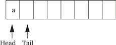
The elastic buffer allows the input and output devices to run at different rates. The queue io_buf acts as a wraparound buffer—we add characters to the tail when an input is received and take characters from the tail when we are ready for output. The head and tail wrap around the end of the buffer array to make most efficient use of the array. Here is the situation at the start of the program’s execution, where the tail points to the first available character and the head points to the ready character. As seen below, because the head and tail are equal, we know that the queue is empty.
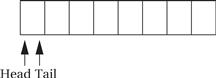
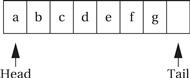
When the first character is read, the tail is incremented after the character is added to the queue, leaving the buffer and pointers looking like the following:
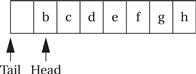
When the buffer is full, we leave one character in the buffer unused. As the next figure shows, if we added another character and updated the tail buffer (wrapping it around to the head of the buffer), we would be unable to distinguish a full buffer from an empty one.
Here is what happens when the output goes past the end of io_buf:
This code implements the elastic buffer, including the declarations for the above global variables and some service routines for adding and removing characters from the queue. Because interrupt handlers are regular code, we can use subroutines to structure code just as with any program.
#define BUF_SIZE 8
char io_buf[BUF_SIZE]; /* character buffer */
int buf_head = 0, buf_tail = 0; /* current position in buffer */
int error = 0; /* set to 1 if buffer ever overflows */
void empty_buffer() { /* returns TRUE if buffer is empty */
buf_head == buf_tail;
}
void full_buffer() { /* returns TRUE if buffer is full */
(buf_tail+1) % BUF_SIZE == buf_head ;
}
int nchars() { /* returns the number of characters in the buffer */
if (buf_head >= buf_tail) return buf_head – buf_tail;
else return BUF_SIZE – buf_tail – buf_head;
}
void add_char(char achar) { /* add a character to the buffer head */
io_buf[buf_tail++] = achar;
/* check pointer */
if (buf_tail == BUF_SIZE)
buf_tail = 0;
}
char remove_char() { /* take a character from the buffer head */
char achar;
achar = io_buf[buf_head++];
/* check pointer */
if (buf_head == BUF_SIZE)
buf_head = 0;
}
Assume that we have two interrupt handling routines defined in C, input_handler for the input device and output_handler for the output device. These routines work with the device in much the same way as did the busy-wait routines. The only complication is in starting the output device: If io_buf has characters waiting, the output driver can start a new output transaction by itself. But if there are no characters waiting, an outside agent must start a new output action whenever the new character arrives. Rather than force the foreground program to look at the character buffer, we will have the input handler check to see whether there is only one character in the buffer and start a new transaction.
Here is the code for the input handler:
#define IN_DATA 0x1000
#define IN_STATUS 0x1001
void input_handler() {
char achar;
if (full_buffer()) /* error */
error = 1;
else { /* read the character and update pointer */
achar = peek(IN_DATA); /* read character */
add_char(achar); /* add to queue */
}
poke(IN_STATUS,0); /* set status register back to 0 */
/* if buffer was empty, start a new output transaction */
if (nchars() == 1) { /* buffer had been empty until this interrupt */
poke(OUT_DATA,remove_char()); /* send character */
poke(OUT_STATUS,1); /* turn device on */
}
}
#define OUT_DATA 0x1100
#define OUT_STATUS 0x1101
void output_handler() {
if (!empty_buffer()) { /* start a new character */
poke(OUT_DATA,remove_char()); /* send character */
poke(OUT_STATUS,1); /* turn device on */
}
}
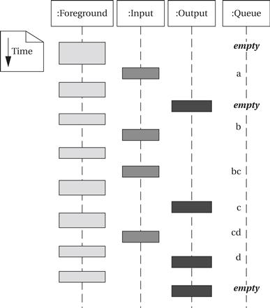
The foreground program does not need to do anything—everything is taken care of by the interrupt handlers. The foreground program is free to do useful work as it is occasionally interrupted by input and output operations. The following sample execution of the program in the form of a UML sequence diagram shows how input and output are interleaved with the foreground program. (We have kept the last input character in the queue until output is complete to make it clearer when input occurs.) The simulation shows that the foreground program is not executing continuously, but it continues to run in its regular state independent of the number of characters waiting in the queue.
Interrupts allow a lot of concurrency, which can make very efficient use of the CPU. But when the interrupt handlers are buggy, the errors can be very hard to find. The fact that an interrupt can occur at any time means that the same bug can manifest itself in different ways when the interrupt handler interrupts different segments of the foreground program.
Example 3.6 illustrates the problems inherent in debugging interrupt handlers.
Example 3.6 Debugging Interrupt Code
Assume that the foreground code is performing a matrix multiplication operation y = Ax + b:
for (i = 0; i < M; i++) {
y[i] = b[i];
for (j = 0; j < N; j++)
y[i] = y[i] + A[i,j]*x[j];
}
We use the interrupt handlers of Example 3.6 to perform I/O while the matrix computation is performed, but with one small change: read_handler has a bug that causes it to change the value of j. While this may seem far-fetched, remember that when the interrupt handler is written in assembly language such bugs are easy to introduce. Any CPU register that is written by the interrupt handler must be saved before it is modified and restored before the handler exits. Any type of bug—such as forgetting to save the register or to properly restore it—can cause that register to mysteriously change value in the foreground program.
What happens to the foreground program when j changes value during an interrupt depends on when the interrupt handler executes. Because the value of j is reset at each iteration of the outer loop, the bug will affect only one entry of the result y. But clearly the entry that changes will depend on when the interrupt occurs. Furthermore, the change observed in y depends on not only what new value is assigned to j (which may depend on the data handled by the interrupt code), but also when in the inner loop the interrupt occurs. An interrupt at the beginning of the inner loop will give a different result than one that occurs near the end. The number of possible new values for the result vector is much too large to consider manually—the bug can’t be found by enumerating the possible wrong values and correlating them with a given root cause. Even recognizing the error can be difficult—for example, an interrupt that occurs at the very end of the inner loop will not cause any change in the foreground program’s result. Finding such bugs generally requires a great deal of tedious experimentation and frustration.
The CPU implements interrupts by checking the interrupt request line at the beginning of execution of every instruction. If an interrupt request has been asserted, the CPU does not fetch the instruction pointed to by the PC. Instead the CPU sets the PC to a predefined location, which is the beginning of the interrupt handling routine. The starting address of the interrupt handler is usually given as a pointer—rather than defining a fixed location for the handler, the CPU defines a location in memory that holds the address of the handler, which can then reside anywhere in memory.
Interrupts and subroutines
Because the CPU checks for interrupts at every instruction, it can respond quickly to service requests from devices. However, the interrupt handler must return to the foreground program without disturbing the foreground program’s operation. Because subroutines perform a similar function, it is natural to build the CPU’s interrupt mechanism to resemble its subroutine function. Most CPUs use the same basic mechanism for remembering the foreground program’s PC as is used for subroutines. The subroutine call mechanism in modern microprocessors is typically a stack, so the interrupt mechanism puts the return address on a stack; some CPUs use the same stack as for subroutines while others define a special stack. The use of a procedure-like interface also makes it easier to provide a high-level language interface for interrupt handlers. The details of the C interface to interrupt handling routines vary both with the CPU and the underlying support software.
Priorities and Vectors
Providing a practical interrupt system requires having more than a simple interrupt request line. Most systems have more than one I/O device, so there must be some mechanism for allowing multiple devices to interrupt. We also want to have flexibility in the locations of the interrupt handling routines, the addresses for devices, and so on. There are two ways in which interrupts can be generalized to handle multiple devices and to provide more flexible definitions for the associated hardware and software:
• interrupt priorities allow the CPU to recognize some interrupts as more important than others, and
• interrupt vectors allow the interrupting device to specify its handler.
Prioritized interrupts not only allow multiple devices to be connected to the interrupt line but also allow the CPU to ignore less important interrupt requests while it handles more important requests. As shown in Figure 3.3, the CPU provides several different interrupt request signals, shown here as L1, L2, up to Ln. Typically, the lower-numbered interrupt lines are given higher priority, so in this case, if devices 1, 2, and n all requested interrupts simultaneously, 1’s request would be acknowledged because it is connected to the highest-priority interrupt line. Rather than provide a separate interrupt acknowledge line for each device, most CPUs use a set of signals that provide the priority number of the winning interrupt in binary form (so that interrupt level 7 requires 3 bits rather than 7). A device knows that its interrupt request was accepted by seeing its own priority number on the interrupt acknowledge lines.
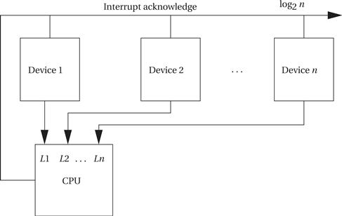
Figure 3.3 Prioritized device interrupts.
How do we change the priority of a device? Simply by connecting it to a different interrupt request line. This requires hardware modification, so if priorities need to be changeable, removable cards, programmable switches, or some other mechanism should be provided to make the change easy.
The priority mechanism must ensure that a lower-priority interrupt does not occur when a higher-priority interrupt is being handled. The decision process is known as masking. When an interrupt is acknowledged, the CPU stores in an internal register the priority level of that interrupt. When a subsequent interrupt is received, its priority is checked against the priority register; the new request is acknowledged only if it has higher priority than the currently pending interrupt. When the interrupt handler exits, the priority register must be reset. The need to reset the priority register is one reason why most architectures introduce a specialized instruction to return from interrupts rather than using the standard subroutine return instruction.
Power-down interrupts
The highest-priority interrupt is normally called the nonmaskable interrupt or NMI. The NMI cannot be turned off and is usually reserved for interrupts caused by power failures—a simple circuit can be used to detect a dangerously low power supply, and the NMI interrupt handler can be used to save critical state in nonvolatile memory, turn off I/O devices to eliminate spurious device operation during power-down,and so on.
Most CPUs provide a relatively small number of interrupt priority levels, such as eight. While more priority levels can be added with external logic, they may not be necessary in all cases. When several devices naturally assume the same priority (such as when you have several identical keypads attached to a single CPU), you can combine polling with prioritized interrupts to efficiently handle the devices. As shown in Figure 3.4, you can use a small amount of logic external to the CPU to generate an interrupt whenever any of the devices you want to group together request service. The CPU will call the interrupt handler associated with this priority; that handler does not know which of the devices actually requested the interrupt. The handler uses software polling to check the status of each device: In this example, it would read the status registers of 1, 2, and 3 to see which of them is ready and requesting service.
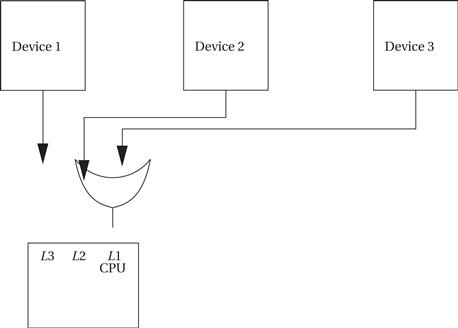
Figure 3.4 Using polling to share an interrupt over several devices.
Example 3.7 Illustrates how priorities affect the order in which I/O requests are handled.
Example 3.7 I/O with Prioritized Interrupts
Assume that we have devices A, B, and C. A has priority 1 (highest priority), B priority 2, and C priority 3. This UML sequence diagram shows which interrupt handler is executing as a function of time for a sequence of interrupt requests:
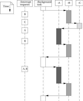
In each case, an interrupt handler keeps running until either it is finished or a higher-priority interrupt arrives. The C interrupt, although it arrives early, does not finish for a long time because interrupts from both A and B intervene—system design must take into account the worst-case combinations of interrupts that can occur to ensure that no device goes without service for too long. When both A and B interrupt simultaneously, A’s interrupt gets priority; when A’s handler is finished, the priority mechanism automatically answers B’s pending interrupt.
Vectors provide flexibility in a different dimension, namely, the ability to define the interrupt handler that should service a request from a device. Figure 3.5 shows the hardware structure required to support interrupt vectors. In addition to the interrupt request and acknowledge lines, additional interrupt vector lines run from the devices to the CPU. After a device’s request is acknowledged, it sends its interrupt vector over those lines to the CPU. The CPU then uses the vector number as an index in a table stored in memory as shown in Figure 3.5. The location referenced in the interrupt vector table by the vector number gives the address of the handler.
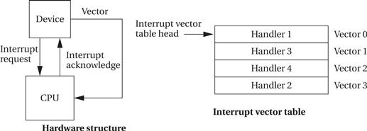
Figure 3.5 Interrupt vectors.
There are two important things to notice about the interrupt vector mechanism. First, the device, not the CPU, stores its vector number. In this way, a device can be given a new handler simply by changing the vector number it sends, without modifying the system software. For example, vector numbers can be changed by programmable switches. The second thing to notice is that there is no fixed relationship between vector numbers and interrupt handlers. The interrupt vector table allows arbitrary relationships between devices and handlers. The vector mechanism provides great flexibility in the coupling of hardware devices and the software routines that service them.
Most modern CPUs implement both prioritized and vectored interrupts. Priorities determine which device is serviced first, and vectors determine what routine is used to service the interrupt. The combination of the two provides a rich interface between hardware and software:
Interrupt Overhead
Now that we have a basic understanding of the interrupt mechanism, we can consider the complete interrupt handling process. Once a device requests an interrupt, some steps are performed by the CPU, some by the device, and others by software:
1. CPU: The CPU checks for pending interrupts at the beginning of an instruction. It answers the highest-priority interrupt, which has a higher priority than that given in the interrupt priority register.
2. Device: The device receives the acknowledgment and sends the CPU its interrupt vector.
3. CPU: The CPU looks up the device handler address in the interrupt vector table using the vector as an index. A subroutine-like mechanism is used to save the current value of the PC and possibly other internal CPU state, such as general-purpose registers.
4. Software: The device driver may save additional CPU state. It then performs the required operations on the device. It then restores any saved state and executes the interrupt return instruction.
5. CPU: The interrupt return instruction restores the PC and other automatically saved states to return execution to the code that was interrupted.
Interrupts do not come without a performance penalty. In addition to the execution time required for the code that talks directly to the devices, there is execution time overhead associated with the interrupt mechanism:
• The interrupt itself has overhead similar to a subroutine call. Because an interrupt causes a change in the program counter, it incurs a branch penalty. In addition, if the interrupt automatically stores CPU registers, that action requires extra cycles, even if the state is not modified by the interrupt handler.
• In addition to the branch delay penalty, the interrupt requires extra cycles to acknowledge the interrupt and obtain the vector from the device.
• The interrupt handler will, in general, save and restore CPU registers that were not automatically saved by the interrupt.
• The interrupt return instruction incurs a branch penalty as well as the time required to restore the automatically saved state.
The time required for the hardware to respond to the interrupt, obtain the vector, and so on cannot be changed by the programmer. In particular, CPUs vary quite a bit in the amount of internal state automatically saved by an interrupt. The programmer does have control over what state is modified by the interrupt handler and therefore it must be saved and restored. Careful programming can sometimes result in a small number of registers used by an interrupt handler, thereby saving time in maintaining the CPU state. However, such tricks usually require coding the interrupt handler in assembly language rather than a high-level language.
Interrupts in ARM
ARM7 supports two types of interrupts: fast interrupt requests (FIQs) and interrupt requests (IRQs). An FIQ takes priority over an IRQ. The interrupt table is always kept in the bottom memory addresses, starting at location 0. The entries in the table typically contain subroutine calls to the appropriate handler.
The ARM7 performs the following steps when responding to an interrupt [ARM99B]:
• saves the appropriate value of the PC to be used to return,
• copies the CPSR into an SPSR (saved program status register),
When leaving the interrupt handler, the handler should:
The worst-case latency to respond to an interrupt includes the following components:
• two cycles to synchronize the external request,
• up to 20 cycles to complete the current instruction,
This adds up to 27 clock cycles. The best-case latency is 4 clock cycles.
Interrupts in C55x
Interrupts in the C55x [Tex04] take at least 7 clock cycles. In many situations, they take 13 clock cycles.
• A maskable interrupt is processed in several steps once the interrupt request is sent to the CPU:
• The interrupt flag register (IFR) corresponding to the interrupt is set.
• The interrupt enable register (IER) is checked to ensure that the interrupt is enabled.
• The interrupt mask register (INTM) is checked to be sure that the interrupt is not masked.
• The interrupt flag register (IFR) corresponding to the flag is cleared.
• Appropriate registers are saved as context.
• INTM is set to 1 to disable maskable interrupts.
• DGBM is set to 1 to disable debug events.
• EALLOW is set to 0 to disable access to non-CPU emulation registers.
• A branch is performed to the interrupt service routine (ISR).
The C55x provides two mechanisms—fast-return and slow-return—to save and restore registers for interrupts and other context switches. Both processes save the return address and loop context registers. The fast-return mode uses RETA to save the return address and CFCT for the loop context bits. The slow-return mode, in contrast, saves the return address and loop context bits on the stack.
Interrupts in PIC16F
The PIC16F recognizes two types of interrupts. Synchronous interrupts generally occur from sources inside the CPU. Asynchronous interrupts are generally triggered from outside the CPU. The INTCON register contains the major control bits for the interrupt system. The Global Interrupt Enable bit GIE is used to allow all unmasked interrupts. The Peripheral Interrupt Enable bit PEIE enables/disables interrupts from peripherals. The TMR0 Overflow Interrupt Enable bit enables or disables the timer 0 overflow interrupt. The INT External Interrupt Enable bit enables/disables the INT external interrupts. Peripheral Interrupt Flag registers PIR1 and PIR2 hold flags for peripheral interrupts.
The RETFIE instruction is used to return from an interrupt routine. This instruction clears the GIE bit, re-enabling pending interrupts.
The latency of synchronous interrupts is 3TCY (where TCY is the length of an instruction) while the latency for asynchronous interrupts is 3 to 3.75TCY. One-cycle and two-cycle instructions have the same interrupt latencies.
3.3 Supervisor Mode, Exceptions, and Traps
In this section we consider exceptions and traps. These are mechanisms to handle internal conditions and they are very similar to interrupts in form. We begin with a discussion of supervisor mode, which some processors use to handle exceptional events and protect executing programs from each other.
3.3.1 Supervisor Mode
As will become clearer in later chapters, complex systems are often implemented as several programs that communicate with each other. These programs may run under the command of an operating system. It may be desirable to provide hardware checks to ensure that the programs do not interfere with each other—for example, by erroneously writing into a segment of memory used by another program. Software debugging is important but can leave some problems in a running system; hardware checks ensure an additional level of safety.
In such cases it is often useful to have a supervisor mode provided by the CPU. Normal programs run in user mode. The supervisor mode has privileges that user modes do not. For example, we will study memory management systems in 3.5 that allow the physical addresses of memory locations to be changed dynamically. Control of the memory management unit is typically reserved for supervisor mode to avoid the obvious problems that could occur when program bugs cause inadvertent changes in the memory management registers, effectively moving code and data in the middle of program execution.
ARM supervisor mode
Not all CPUs have supervisor modes. Many DSPs, including the C55x, do not provide one. The ARM, however, does have a supervisor mode. The ARM instruction that puts the CPU in supervisor mode is called SWI:
SWI CODE_1
It can, of course, be executed conditionally, as with any ARM instruction. SWI causes the CPU to go into supervisor mode and sets the PC to 0x08. The argument to SWI is a 24-bit immediate value that is passed on to the supervisor mode code; it allows the program to request various services from the supervisor mode.
In supervisor mode, the bottom five bits of the CPSR are all set to 1 to indicate that the CPU is in supervisor mode. The old value of the CPSR just before the SWI is stored in a register is called the saved program status register (SPSR). There are in fact several SPSRs for different modes; the supervisor mode SPSR is referred to as SPSR_svc.
To return from supervisor mode, the supervisor restores the PC from register r14 and restores the CPSR from the SPSR_svc.
3.3.2 Exceptions
An exception is an internally detected error. A simple example is division by zero. One way to handle this problem would be to check every divisor before division to be sure it is not zero, but this would both substantially increase the size of numerical programs and cost a great deal of CPU time evaluating the divisor’s value. The CPU can more efficiently check the divisor’s value during execution. Because the time at which a zero divisor will be found is not known in advance, this event is similar to an interrupt except that it is generated inside the CPU. The exception mechanism provides a way for the program to react to such unexpected events. Resets, undefined instructions, and illegal memory accesses are other typical examples of exceptions.
Just as interrupts can be seen as an extension of the subroutine mechanism, exceptions are generally implemented as a variation of an interrupt. Because both deal with changes in the flow of control of a program, it makes sense to use similar mechanisms. However, exceptions are generated internally.
Exceptions in general require both prioritization and vectoring. Exceptions must be prioritized because a single operation may generate more than one exception—for example, an illegal operand and an illegal memory access. The priority of exceptions is usually fixed by the CPU architecture. Vectoring provides a way for the user to specify the handler for the exception condition. The vector number for an exception is usually predefined by the architecture; it is used to index into a table of exception handlers.
3.3.3 Traps
A trap, also known as a software interrupt, is an instruction that explicitly generates an exception condition. The most common use of a trap is to enter supervisor mode. The entry into supervisor mode must be controlled to maintain security—if the interface between user and supervisor mode is improperly designed, a user program may be able to sneak code into the supervisor mode that could be executed to perform harmful operations.
The ARM provides the SWI interrupt for software interrupts. This instruction causes the CPU to enter supervisor mode. An opcode is embedded in the instruction that can be read by the handler.
3.4 Co-Processors
CPU architects often want to provide flexibility in what features are implemented in the CPU. One way to provide such flexibility at the instruction set level is to allow co-processors, which are attached to the CPU and implement some of the instructions. For example, floating-point arithmetic was introduced into the Intel architecture by providing separate chips that implemented the floating-point instructions.
To support co-processors, certain opcodes must be reserved in the instruction set for co-processor operations. Because it executes instructions, a co-processor must be tightly coupled to the CPU. When the CPU receives a co-processor instruction, the CPU must activate the co-processor and pass it the relevant instruction. Co-processor instructions can load and store co-processor registers or can perform internal operations. The CPU can suspend execution to wait for the co-processor instruction to finish; it can also take a more superscalar approach and continue executing instructions while waiting for the co-processor to finish.
A CPU may, of course, receive co-processor instructions even when there is no co-processor attached. Most architectures use illegal instruction traps to handle these situations. The trap handler can detect the co-processor instruction and, for example, execute it in software on the main CPU. Emulating co-processor instructions in software is slower but provides compatibility.
Co-processors in ARM
The ARM architecture provides support for up to 16 co-processors attached to a CPU. Co-processors are able to perform load and store operations on their own registers. They can also move data between the co-processor registers and main ARM registers.
An example ARM co-processor is the floating-point unit. The unit occupies two co-processor units in the ARM architecture, numbered 1 and 2, but it appears as a single unit to the programmer. It provides eight 80-bit floating-point data registers, floating-point status registers, and an optional floating-point status register.
3.5 Memory System Mechanisms
Modern microprocessors do more than just read and write a monolithic memory. Architectural features improve both the speed and capacity of memory systems. Microprocessor clock rates are increasing at a faster rate than memory speeds, such that memories are falling further and further behind microprocessors every day. As a result, computer architects resort to caches to increase the average performance of the memory system. Although memory capacity is increasing steadily, program sizes are increasing as well, and designers may not be willing to pay for all the memory demanded by an application. Memory management units (MMUs) perform address translations that provide a larger virtual memory space in a small physical memory. In this section, we review both caches and MMUs.
3.5.1 Caches
Caches are widely used to speed up reads and writes in memory systems. Many microprocessor architectures include caches as part of their definition. The cache speeds up average memory access time when properly used. It increases the variability of memory access times—accesses in the cache will be fast, while access to locations not cached will be slow. This variability in performance makes it especially important to understand how caches work so that we can better understand how to predict cache performance and factor these variations into system design.
Cache controllers
A cache is a small, fast memory that holds copies of some of the contents of main memory. Because the cache is fast, it provides higher-speed access for the CPU; but because it is small, not all requests can be satisfied by the cache, forcing the system to wait for the slower main memory. Caching makes sense when the CPU is using only a relatively small set of memory locations at any one time; the set of active locations is often called the working set.
Figure 3.6 shows how the cache supports reads in the memory system. A cache controller mediates between the CPU and the memory system comprised of the cache and main memory. The cache controller sends a memory request to the cache and main memory. If the requested location is in the cache, the cache controller forwards the location’s contents to the CPU and aborts the main memory request; this condition is known as a cache hit. If the location is not in the cache, the controller waits for the value from main memory and forwards it to the CPU; this situation is known as a cache miss.
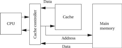
Figure 3.6 The cache in the memory system.
We can classify cache misses into several types depending on the situation that generated them:
• a compulsory miss (also known as a cold miss) occurs the first time a location is used,
• a capacity miss is caused by a too-large working set, and
• a conflict miss happens when two locations map to the same location in the cache.
Memory system performance
Even before we consider ways to implement caches, we can write some basic formulas for memory system performance. Let h be the hit rate, the probability that a given memory location is in the cache. It follows that 1 – h is the miss rate, or the probability that the location is not in the cache. Then we can compute the average memory access time as
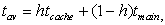 (Eq. 3.1)
where tcache is the access time of the cache and tmain is the main memory access time. The memory access times are basic parameters available from the memory manufacturer. The hit rate depends on the program being executed and the cache organization, and is typically measured using simulators. The best-case memory access time (ignoring cache controller overhead) is tcache , while the worst-case access time is tmain . Given that tmain is typically 50 to 75 ns, while tcache is at most a few nanoseconds, the spread between worst-case and best-case memory delays is substantial.
First- and second-level cache
Modern CPUs may use multiple levels of cache as shown in Figure 3.7. The first-level cache (commonly known as L1 cache) is closest to the CPU, the second-level cache (L2 cache) feeds the first-level cache, and so on. In today’s microprocessors, the first-level cache is often on-chip and the second-level cache is off-chip, although we are starting to see on-chip second-level caches.
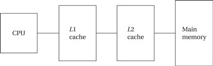
Figure 3.7 A two-level cache system.
The second-level cache is much larger but is also slower. If h1 is the first-level hit rate and h2 is the rate at which access hit the second-level cache, then the average access time for a two-level cache system is
 (Eq. 3.2)
As the program’s working set changes, we expect locations to be removed from the cache to make way for new locations. When set-associative caches are used, we have to think about what happens when we throw out a value from the cache to make room for a new value. We do not have this problem in direct-mapped caches because every location maps onto a unique block, but in a set-associative cache we must decide which set will have its block thrown out to make way for the new block. One possible replacement policy is least recently used (LRU), that is, throw out the block that has been used farthest in the past. We can add relatively small amounts of hardware to the cache to keep track of the time since the last access for each block. Another policy is random replacement, which requires even less hardware to implement.
Cache organization
The simplest way to implement a cache is a direct-mapped cache, as shown in Figure 3.8. The cache consists of cache blocks, each of which includes a tag to show which memory location is represented by this block, a data field holding the contents of that memory, and a valid tag to show whether the contents of this cache block are valid. An address is divided into three sections. The index is used to select which cache block to check. The tag is compared against the tag value in the block selected by the index. If the address tag matches the tag value in the block, that block includes the desired memory location. If the length of the data field is longer than the minimum addressable unit, then the lowest bits of the address are used as an offset to select the required value from the data field. Given the structure of the cache, there is only one block that must be checked to see whether a location is in the cache—the index uniquely determines that block. If the access is a hit, the data value is read from the cache.
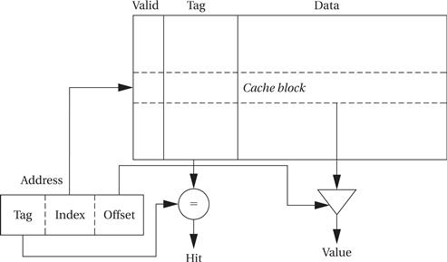
Figure 3.8 A direct-mapped cache.
Writes are slightly more complicated than reads because we have to update main memory as well as the cache. There are several methods by which we can do this. The simplest scheme is known as write-through—every write changes both the cache and the corresponding main memory location (usually through a write buffer). This scheme ensures that the cache and main memory are consistent, but may generate some additional main memory traffic. We can reduce the number of times we write to main memory by using a write-back policy: If we write only when we remove a location from the cache, we eliminate the writes when a location is written several times before it is removed from the cache.
The direct-mapped cache is both fast and relatively low cost, but it does have limits in its caching power due to its simple scheme for mapping the cache onto main memory. Consider a direct-mapped cache with four blocks, in which locations 0, 1, 2, and 3 all map to different blocks. But locations 4, 8, 12, … all map to the same block as location 0; locations 1, 5, 9, 13, … all map to a single block; and so on. If two popular locations in a program happen to map onto the same block, we will not gain the full benefits of the cache. As seen in Section 5.7, this can create program performance problems.
The limitations of the direct-mapped cache can be reduced by going to the set-associative cache structure shown in Figure 3.9. A set-associative cache is characterized by the number of banks or ways it uses, giving an n-way set-associative cache. A set is formed by all the blocks (one for each bank) that share the same index. Each set is implemented with a direct-mapped cache. A cache request is broadcast to all banks simultaneously. If any of the sets has the location, the cache reports a hit. Although memory locations map onto blocks using the same function, there are n separate blocks for each set of locations. Therefore, we can simultaneously cache several locations that happen to map onto the same cache block. The set-associative cache structure incurs a little extra overhead and is slightly slower than a direct-mapped cache, but the higher hit rates that it can provide often compensate.
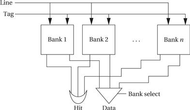
Figure 3.9 A set-associative cache.
The set-associative cache generally provides higher hit rates than the direct-mapped cache because conflicts between a small set of locations can be resolved within the cache. The set-associative cache is somewhat slower, so the CPU designer has to be careful that it doesn’t slow down the CPU’s cycle time too much. A more important problem with set-associative caches for embedded program design is predictability. Because the time penalty for a cache miss is so severe, we often want to make sure that critical segments of our programs have good behavior in the cache. It is relatively easy to determine when two memory locations will conflict in a direct-mapped cache. Conflicts in a set-associative cache are more subtle, and so the behavior of a set-associative cache is more difficult to analyze for both humans and programs.
Example 3.8 compares the behavior of direct-mapped and set-associative caches.
Example 3.8 Direct-Mapped versus Set-Associative Caches
For simplicity, let’s consider a very simple caching scheme. We use two bits of the address as the tag. We compare a direct-mapped cache with four blocks and a two-way set-associative cache with four sets, and we use LRU replacement to make it easy to compare the two caches.
Here are the contents of memory, using a three-bit address for simplicity:
| Address | Data |
| 000 | 0101 |
| 001 | 1111 |
| 010 | 0000 |
| 011 | 0110 |
| 100 | 1000 |
| 101 | 0001 |
| 110 | 1010 |
| 111 | 0100 |
We will give each cache the same pattern of addresses (in binary to simplify picking out the index): 001, 010, 011, 100, 101, and 111. To understand how the direct-mapped cache works, let’s see how its state evolves.
After 001 access:
| Block | Tag | Data |
| 00 | — | — |
| 01 | 0 | 1111 |
| 10 | — | — |
| 11 | — | — |
After 010 access:
| Block | Tag | Data |
| 00 | — | — |
| 01 | 0 | 1111 |
| 10 | 0 | 0000 |
| 11 | — |
After 011 access:
| Block | Tag | Data |
| 00 | — | — |
| 01 | 0 | 1111 |
| 10 | 0 | 0000 |
| 11 | 0 | 0110 |
After 100 access (notice that the tag bit for this entry is 1):
| Block | Tag | Data |
| 00 | 1 | 1000 |
| 01 | 0 | 1111 |
| 10 | 0 | 0000 |
| 11 | 0 | 0110 |
After 101 access (overwrites the 01 block entry):
| Block | Tag | Data |
| 00 | 1 | 1000 |
| 01 | 1 | 0001 |
| 10 | 0 | 0000 |
| 11 | 0 | 0110 |
After 111 access (overwrites the 11 block entry):
| Block | Tag | Data |
| 00 | 1 | 1000 |
| 01 | 1 | 0001 |
| 10 | 0 | 0000 |
| 11 | 1 | 0100 |
We can use a similar procedure to determine what ends up in the two-way set-associative cache. The only difference is that we have some freedom when we have to replace a block with new data. To make the results easy to understand, we use a least-recently-used replacement policy. For starters, let’s make each bank the size of the original direct-mapped cache. The final state of the two-way set-associative cache follows:
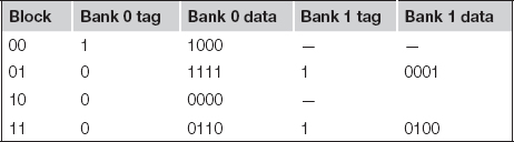
Of course, this isn’t a fair comparison for performance because the two-way set-associative cache has twice as many entries as the direct-mapped cache. Let’s use a two-way, set-associative cache with two sets, giving us four blocks, the same number as in the direct-mapped cache. In this case, the index size is reduced to one bit and the tag grows to two bits.
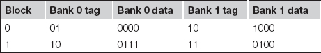
In this case, the cache contents significantly differ from either the direct-mapped cache or the four-block, two-way set-associative cache.
The CPU knows when it is fetching an instruction (the PC is used to calculate the address, either directly or indirectly) or data. We can therefore choose whether to cache instructions, data, or both. If cache space is limited, instructions are the highest priority for caching because they will usually provide the highest hit rates. A cache that holds both instructions and data is called a unified cache.
ARM caches
Various ARM implementations use different cache sizes and organizations [Fur96]. The ARM600 includes a 4-Kbyte, 64-way (wow!) unified instruction/data cache. The StrongARM uses a 16-Kbyte, 32-way instruction cache with a 32-byte block and a 16-Kbyte, 32-way data cache with a 32-byte block; the data cache uses a write-back strategy.
C55x caches
The C5510, one of the models of C55x, uses a 16-Kbyte instruction cache organized as a two-way set-associative cache with four 32-bit words per line. The instruction cache can be disabled by software if desired. It also includes two RAM sets that are designed to hold large contiguous blocks of code. Each RAM set can hold up to 4-Kbytes of code organized as 256 lines of four 32-bit words per line. Each RAM has a tag that specifies what range of addresses are in the RAM; it also includes a tag valid field to show whether the RAM is in use and line valid bits for each line.
3.5.2 Memory Management Units and Address Translation
A memory management unit translates addresses between the CPU and physical memory. This translation process is often known as memory mapping because addresses are mapped from a logical space into a physical space. Memory management units are not especially common in embedded systems because virtual memory requires a secondary storage device such as a disk. However, that situation is slowly changing with lower component prices in general and the advent of Internet appliances in particular. It is helpful to understand the basics of MMUs for embedded systems complex enough to require them.
Many DSPs, including the C55x, don’t use MMUs. Because DSPs are used for compute-intensive tasks, they often don’t require the hardware assist for logical address spaces.
Memory mapping philosophy
Early computers used MMUs to compensate for limited address space in their instruction sets. When memory became cheap enough that physical memory could be larger than the address space defined by the instructions, MMUs allowed software to manage multiple programs in a single physical memory, each with its own address space.
Virtual addressing
Because modern CPUs typically do not have this limitation, MMUs are used to provide virtual addressing. As shown in Figure 3.10, the memory management unit accepts logical addresses from the CPU. Logical addresses refer to the program’s abstract address space but do not correspond to actual RAM locations. The MMU translates them from tables to physical addresses that do correspond to RAM. By changing the MMU’s tables, you can change the physical location at which the program resides without modifying the program’s code or data. (We must, of course, move the program in main memory to correspond to the memory mapping change.)
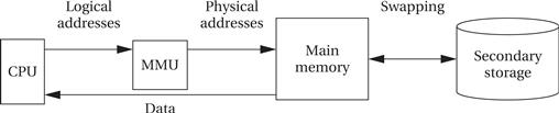
Figure 3.10 A virtually addressed memory system.
Furthermore, if we add a secondary storage unit such as a disk, we can eliminate parts of the program from main memory. In a virtual memory system, the MMU keeps track of which logical addresses are actually resident in main memory; those that do not reside in main memory are kept on the secondary storage device. When the CPU requests an address that is not in main memory, the MMU generates an exception called a page fault. The handler for this exception executes code that reads the requested location from the secondary storage device into main memory. The program that generated the page fault is restarted by the handler only after
• the required memory has been read back into main memory, and
• the MMU’s tables have been updated to reflect the changes.
Of course, loading a location into main memory will usually require throwing something out of main memory. The displaced memory is copied into secondary storage before the requested location is read in. As with caches, LRU is a good replacement policy.
There are two styles of address translation: segmented and paged. Each has advantages and the two can be combined to form a segmented, paged addressing scheme. As illustrated in Figure 3.11, segmenting is designed to support a large, arbitrarily sized region of memory, while pages describe small, equally sized regions. A segment is usually described by its start address and size, allowing different segments to be of different sizes. Pages are of uniform size, which simplifies the hardware required for address translation. A segmented, paged scheme is created by dividing each segment into pages and using two steps for address translation. Paging introduces the possibility of fragmentation as program pages are scattered around physical memory.
Figure 3.11 Segments and pages.
In a simple segmenting scheme, shown in Figure 3.12, the MMU would maintain a segment register that describes the currently active segment. This register would point to the base of the current segment. The address extracted from an instruction (or from any other source for addresses, such as a register) would be used as the offset for the address. The physical address is formed by adding the segment base to the offset. Most segmentation schemes also check the physical address against the upper limit of the segment by extending the segment register to include the segment size and comparing the offset to the allowed size.
Figure 3.12 Address translation for a segment.
The translation of paged addresses requires more MMU state but a simpler calculation. As shown in Figure 3.13, the logical address is divided into two sections, including a page number and an offset. The page number is used as an index into a page table, which stores the physical address for the start of each page. However, because all pages have the same size and it is easy to ensure that page boundaries fall on the proper boundaries, the MMU simply needs to concatenate the top bits of the page starting address with the bottom bits from the page offset to form the physical address. Pages are small, typically between 512 bytes to 4 KB. As a result, an architecture with a large address space requires a large page table. The page table is normally kept in main memory, which means that an address translation requires memory access.
Figure 3.13 Address translation for a page.
The page table may be organized in several ways, as shown in Figure 3.14. The simplest scheme is a flat table. The table is indexed by the page number and each entry holds the page descriptor. A more sophisticated method is a tree. The root entry of the tree holds pointers to pointer tables at the next level of the tree; each pointer table is indexed by a part of the page number. We eventually (after three levels, in this case) arrive at a descriptor table that includes the page descriptor we are interested in. A tree-structured page table incurs some overhead for the pointers, but it allows us to build a partially populated tree. If some part of the address space is not used, we do not need to build the part of the tree that covers it.
Figure 3.14 Alternative schemes for organizing page tables.
The efficiency of paged address translation may be increased by caching page translation information. A cache for address translation is known as a translation lookaside buffer (TLB). The MMU reads the TLB to check whether a page number is currently in the TLB cache and, if so, uses that value rather than reading from memory.
Virtual memory is typically implemented in a paging or segmented, paged scheme so that only page-sized regions of memory need to be transferred on a page fault. Some extensions to both segmenting and paging are useful for virtual memory:
• At minimum, a present bit is necessary to show whether the logical segment or page is currently in physical memory.
• A dirty bit shows whether the page/segment has been written to. This bit is maintained by the MMU, because it knows about every write performed by the CPU.
• Permission bits are often used. Some pages/segments may be readable but not writable. If the CPU supports modes, pages/segments may be accessible by the supervisor but not in user mode.
A data or instruction cache may operate either on logical or physical addresses, depending on where it is positioned relative to the MMU.
A memory management unit is an optional part of the ARM architecture. The ARM MMU supports both virtual address translation and memory protection; the architecture requires that the MMU be implemented when cache or write buffers are implemented. The ARM MMU supports the following types of memory regions for address translation:
An address is marked as section mapped or page mapped. A two-level scheme is used to translate addresses. The first-level table, which is pointed to by the Translation Table Base register, holds descriptors for section translation and pointers to the second-level tables. The second-level tables describe the translation of both large and small pages. The basic two-level process for a large or small page is illustrated in Figure 3.15. The details differ between large and small pages, such as the size of the second-level table index. The first- and second-level pages also contain access control bits for virtual memory and protection.
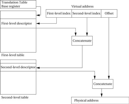
Figure 3.15 ARM two-stage address translation.
3.6 CPU Performance
Now that we have an understanding of the various types of instructions that CPUs can execute, we can move on to a topic particularly important in embedded computing: How fast can the CPU execute instructions? In this section, we consider two factors that can substantially influence program performance: pipelining and caching.
3.6.1 Pipelining
Modern CPUs are designed as pipelined machines in which several instructions are executed in parallel. Pipelining greatly increases the efficiency of the CPU. But like any pipeline, a CPU pipeline works best when its contents flow smoothly. Some sequences of instructions can disrupt the flow of information in the pipeline and, temporarily at least, slow down the operation of the CPU.
ARM7 pipeline
The ARM7 has a three-stage pipeline:
1. Fetch: the instruction is fetched from memory.
2. Decode: the instruction’s opcode and operands are decoded to determine what function to perform.
Each of these operations requires one clock cycle for typical instructions. Thus, a normal instruction requires three clock cycles to completely execute, known as the latency of instruction execution. But because the pipeline has three stages, an instruction is completed in every clock cycle. In other words, the pipeline has a throughput of one instruction per cycle. Figure 3.16 illustrates the position of instructions in the pipeline during execution using the notation introduced by Hennessy and Patterson [Hen06]. A vertical slice through the timeline shows all instructions in the pipeline at that time. By following an instruction horizontally, we can see the progress of its execution.
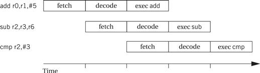
Figure 3.16 Pipelined execution of ARM instructions.
C55x pipeline
The C55x includes a seven-stage pipeline [Tex00B]:
3. Address: computes data and branch addresses.
5. Access 2: finishes data read.
RISC machines are designed to keep the pipeline busy. CISC machines may display a wide variation in instruction timing. Pipelined RISC machines typically have more regular timing characteristics—most instructions that do not have pipeline hazards display the same latency.
Pipeline stalls
The one-cycle-per-instruction completion rate does not hold in every case, however. The simplest case for extended execution is when an instruction is too complex to complete the execution phase in a single cycle. A multiple load instruction is an example of an instruction that requires several cycles in the execution phase. Figure 3.17 illustrates a data stall in the execution of a sequence of instructions starting with a load multiple (LDMIA) instruction. Because there are two registers to load, the instruction must stay in the execution phase for two cycles. In a multiphase execution, the decode stage is also occupied, because it must continue to remember the decoded instruction. As a result, the SUB instruction is fetched at the normal time but not decoded until the LDMIA is finishing. This delays the fetching of the third instruction, the CMP.
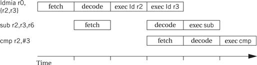
Figure 3.17 Pipelined execution of multicycle ARM instructions.
Branches also introduce control stall delays into the pipeline, commonly referred to as the branch penalty, as shown in Figure 3.18. The decision whether to take the conditional branch BNE is not made until the third clock cycle of that instruction’s execution, which computes the branch target address. If the branch is taken, the succeeding instruction at PC+4 has been fetched and started to be decoded. When the branch is taken, the branch target address is used to fetch the branch target instruction. Because we have to wait for the execution cycle to complete before knowing the target, we must throw away two cycles of work on instructions in the path not taken. The CPU uses the two cycles between starting to fetch the branch target and starting to execute that instruction to finish housekeeping tasks related to the execution of the branch.
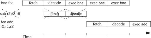
Figure 3.18 Pipelined execution of a branch in ARM.
One way around this problem is to introduce the delayed branch. In this style of branch instruction, a fixed number of instructions directly after the branch are always executed, whether or not the branch is taken. This allows the CPU to keep the pipeline full during execution of the branch. However, some of those instructions after the delayed branch may be no-ops. Any instruction in the delayed branch window must be valid for both execution paths, whether or not the branch is taken. If there are not enough instructions to fill the delayed branch window, it must be filled with no-ops.
Let’s use this knowledge of instruction execution time to develop two examples. First, we will look at execution times on the PIC16F; we will then evaluate the execution time of some C code on the more complex ARM.
Example 3.9 Execution Time of a Loop on the PIC16F
The PIC16F is pipelined but has relatively simple instruction timing [Mic07]. An instruction is divided into four Q cycles:
The time required for an instruction is called Tcy. The CPU executes one Q cycle per clock period. Because instruction execution is pipelined, we generally refer to execution time of an instruction as the number of cycles between it and the next instruction. The PIC16F does not have a cache.
The majority of instructions execute in one cycle. But there are exceptions:
• Several flow-of-control instructions (CALL, GOTO, RETFIE, RETLW, RETURN) always require two cycles.
• Skip-if instructions (DECFSZ, INCFSZ, BTFSC, BTFSS) require two cycles if the skip is taken, one cycle if the skip is not taken. (If the skip is taken, the next instruction remains in the pipeline but is not executed, causing a one-cycle pipeline bubble).
The PIC16F’s very predictable timing allows real-time behavior to be encoded into a program. For example, we can set a bit on an I/O device for a data-dependent amount of time [Mic97B]:
movf len, w ; get ready for computed goto
addwf pcl, f ; computed goto (PCL is low byte of PC)
len3: bsf x,l ; set the bit at t-3
len2: bsf x,l ; set the bit at t-2
len1: bsf x,l ; set the bit at t-1
bcf x,l ; clear the bit at t
A computed goto is a general term for a branch to a location determined by a data value. In this case, the variable len determines the number of clock cycles for which the I/O device bit is set. If we want to set the bit for 3 cycles, we set len to 1 so that the computed goto jumps to len3. If we want to set the device bit for 2 cycles, we set len to 2; to set the device bit for 1 cycle we set len to 3. Setting the device bit multiple times does not harm the operation of the I/O device. The computed goto allows us to vary the I/O device’s operation time dynamically while still maintaining very predictable timing.
Example 3.10 Execution Time of a Loop on the ARM
We will use the C code for the FIR filter of Application Example 2.1:
for (i = 0, f = 0; i < N; i++)
f = f + c[i] * x[i];
We repeat the ARM code for this loop:
;loop initiation code
MOV r0,#0 ;use r0 for i, set to 0
MOV r8,#0 ;use a separate index for arrays
ADR r2,N ;get address for N
LDR r1,[r2] ;get value of N for loop termination test
MOV r2,#0 ;use r2 for f, set to 0
ADR r3,c ;load r3 with address of base of c array
ADR r5,x ;load r5 with address of base of x array
;loop body
loop LDR r4,[r3,r8] ;get value of c[i]
LDR r6,[r5,r8] ;get value of x[i]
MUL r4,r4,r6 ;compute c[i]*x[i]
ADD r2,r2,r4 ;add into running sum f
;update loop counter and array index
ADD r8,r8,#4 ;add one word offset to array index
ADD r0,r0,#1 ;add 1 to i
;test for exit
CMP r0,r1
BLT loop ; if i < N, continue loop
loopend …
Inspection of the code shows that the only instruction that may take more than one cycle is the conditional branch in the loop test. We can count the number of instructions and associated number of clock cycles in each block as follows:
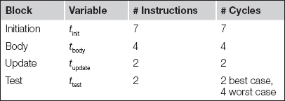
The unconditional branch at the end of the update block always incurs a branch penalty of two cycles. The BLT instruction in the test block incurs a pipeline delay of two cycles when the branch is taken. That happens for all but the last iteration, when the instruction has an execution time of ttest,worst; the last iteration executes in time ttest,best. We can write a formula for the total execution time of the loop in cycles as

3.6.2 Cache Performance
We have already discussed caches functionally. Although caches are invisible in the programming model, they have a profound effect on performance. We introduce caches because they substantially reduce memory access time when the requested location is in the cache. However, the desired location is not always in the cache because it is considerably smaller than main memory. As a result, caches cause the time required to access memory to vary considerably. The extra time required to access a memory location not in the cache is often called the cache miss penalty. The amount of variation depends on several factors in the system architecture, but a cache miss is often several clock cycles slower than a cache hit.
The time required to access a memory location depends on whether the requested location is in the cache. However, as we have seen, a location may not be in the cache for several reasons.
• At a compulsory miss, the location has not been referenced before.
• At a conflict miss, two particular memory locations are fighting for the same cache line.
• At a capacity miss, the program’s working set is simply too large for the cache.
The contents of the cache can change considerably over the course of execution of a program. When we have several programs running concurrently on the CPU, we can have very dramatic changes in the cache contents. We need to examine the behavior of the programs running on the system to be able to accurately estimate performance when caches are involved. We consider this problem in more detail in Section 5.7.
3.7 CPU Power Consumption
Power consumption is, in some situations, as important as execution time. In this section we study the characteristics of CPUs that influence power consumption and mechanisms provided by CPUs to control how much power they consume.
Energy vs. power
First, we need to distinguish between energy and power. Power is, of course, energy consumption per unit time. Heat generation depends on power consumption. Battery life, on the other hand, most directly depends on energy consumption. Generally, we will use the term power as shorthand for energy and power consumption, distinguishing between them only when necessary.
CMOS power characteristics
The high-level power consumption characteristics of CPUs and other system components are derived from the circuits used to build those components. Today, virtually all digital systems are built with CMOS (complementary metal oxide semiconductor) circuitry. The detailed circuit characteristics are best left to a study of VLSI design [Wol08], but the basic sources of CMOS power consumption are easily identified:
• Power supply voltage: The power consumption of a CMOS circuit is proportional to the square of the power supply voltage (V2). Therefore, by reducing the power supply voltage to the lowest level that provides the required performance, we can significantly reduce power consumption. We also may be able to add parallel hardware and even further reduce the power supply voltage while maintaining required performance [Cha92].
• Capacitive toggling: A CMOS circuit uses most of its power when it is changing its output value. This provides two ways to reduce power consumption. By reducing the speed at which the circuit operates, we can reduce its power consumption (although not the total energy required for the operation, because the result is available later). We can actually reduce energy consumption by eliminating unnecessary changes to the inputs of a CMOS circuit—eliminating unnecessary glitches at the circuit outputs eliminates unnecessary power consumption.
• Leakage: Even when a CMOS circuit is not active, some charge leaks out of the circuit’s nodes through the substrate. The only way to eliminate leakage current is to remove the power supply. Completely disconnecting the power supply eliminates power consumption, but it usually takes a significant amount of time to reconnect the system to the power supply and reinitialize its internal state so that it once again performs properly.
As a result, several power-saving strategies are used in CMOS CPUs:
• CPUs can be used at reduced voltage levels. For example, reducing the power supply from 1 V to 0.9 V causes the power consumption to drop by 12/0.92 = 1.2.
• The CPU can be operated at a lower clock frequency to reduce power (but not energy) consumption.
• The CPU may internally disable certain function units that are not required for the currently executing function. This reduces energy consumption.
• Some CPUs allow parts of the CPU to be totally disconnected from the power supply to eliminate leakage currents.
Static vs. dynamic power management
There are two types of power management features provided by CPUs. A static power management mechanism is invoked by the user but does not otherwise depend on CPU activities. An example of a static mechanism is a power-down mode intended to save energy. This mode provides a high-level way to reduce unnecessary power consumption. The mode is typically entered with an instruction. If the mode stops the interpretation of instructions, then it clearly cannot be exited by execution of another instruction. Power-down modes typically end upon receipt of an interrupt or other event. A dynamic power management mechanism takes actions to control power based upon the dynamic activity in the CPU. For example, the CPU may turn off certain sections of the CPU when the instructions being executed do not need them. Application Example 3.2 describes the static and dynamic energy efficiency features of a PowerPC chip.
Application Example 3.2 Energy Efficiency Features in the PowerPC 603
The PowerPC 603 [Gar94] was designed specifically for low-power operation while retaining high performance. It typically dissipates 2.2 W running at 80 MHz. The architecture provides three low-power modes—doze, nap, and sleep—that provide static power management capabilities for use by the programs and operating system.
The 603 also uses a variety of dynamic power management techniques for power minimization that are performed automatically, without program intervention. The CPU is a two-issue, out-of-order superscalar processor. It uses the dynamic techniques summarized below to reduce power consumption.
• An execution unit that is not being used can be shut down.
• The cache, an 8-KB, two-way set-associative cache, was organized into subarrays so that at most two out of eight subarrays will be accessed on any given clock cycle. A variety of circuit techniques were also used in the cache to reduce power consumption.
Not all units in the CPU are active all the time; idling them when they are not being used can save power. The table below shows the percentage of time various units in the 603 were idle for the SPEC integer and floating-point benchmarks [Gar94].
| Unit | Specint92 (% idle) | Specfp92 (% idle) |
| Data cache | 29 | 28 |
| Instruction cache | 29 | 17 |
| Load-store | 35 | 17 |
| Fixed-point | 38 | 76 |
| Floating-point | 99 | 30 |
| System register | 89 | 97 |
Idle units are turned off automatically by switching off their clocks. Various stages of the pipeline are turned on and off, depending on which stages are necessary at the current time. Measurements comparing the chip’s power consumption with and without dynamic power management show that dynamic techniques provide significant power savings.
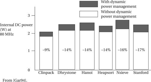
A power-down mode provides the opportunity to greatly reduce power consumption because it will typically be entered for a substantial period of time. However, going into and especially out of a power-down mode is not free—it costs both time and energy. The power-down or power-up transition consumes time and energy in order to properly control the CPU’s internal logic. Modern pipelined processors require complex control that must be properly initialized to avoid corrupting data in the pipeline. Starting up the processor must also be done carefully to avoid power surges that could cause the chip to malfunction or even damage it.
The modes of a CPU can be modeled by a power state machine[Ben00]. An example is shown in Figure 3.19. Each state in the machine represents a different mode of the machine, and every state is labeled with its average power consumption. The example machine has two states: run mode with power consumption Prun and sleep mode with power consumption Psleep. Transitions show how the machine can go from state to state; each transition is labeled with the time required to go from the source to the destination state. In a more complex example, it may not be possible to go from a particular state to another particular state—traversing a sequence of states may be necessary. Application Example 3.3 describes the power-down modes of the StrongARM SA-1100.
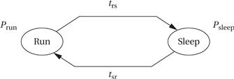
Figure 3.19 A power state machine for a processor.
Application Example 3.3 Power-Saving Modes of the StrongARM SA-1100
The StrongARM SA-1100 [Int99] is designed to provide sophisticated power management capabilities that are controlled by the on-chip power manager. The processor takes two power supplies:
VDD is the main power supply for the core CPU and is nominally 3.3 V. The VDDX supply is used for the pins and other logic such as the power manager; it is normally at 1.5 V. (The two supplies share a common ground.) The system can supply two inputs about the status of the power supply. VDD_FAULT tells the CPU that the main power supply is not being properly regulated, while BATT_FAULT indicates that the battery has been removed or is low. Either of these events can cause the CPU to go into a low-power mode. In low-power operation, the VDD supply can be turned off (the VDDX supply always remains on). When resuming operation, the PWR_EN signal is used by the CPU to tell the external power supply to ramp up the VDD power supply.
A system power manager can both monitor the CPU and other devices and control their operation to gracefully transition between power modes. It provides several registers that allow programs to control power modes, determine why power modes were entered, determine the current state of power management modes, and so on.
The SA-1100 provides the three power modes:
• Run mode is normal operation and has the highest power consumption.
• Idle mode saves power by stopping the CPU clock. The system unit modules—real-time clock, operating system timer, interrupt control, general-purpose I/O, and power manager—all remain operational. Idle mode is entered by executing a three-instruction sequence. The CPU returns to run mode upon receiving an interrupt from one of the internal system units or from a peripheral or by resetting the CPU. This causes the machine to restart the CPU clock and to resume execution where it left off.
• Sleep mode shuts off most of the chip’s activity. Entering sleep mode causes the system to shut down on-chip activity, reset the CPU, and negate the PWR_EN pin to tell the external electronics that the chip’s power supply should be driven to 0 volts. A separate I/O power supply remains on and supplies power to the power manager so that the CPU can be awakened from sleep mode; the low-speed clock keeps the power manager running at low speeds sufficient to manage sleep mode. The CPU software should set several registers to prepare for sleep mode. Sleep mode is entered by forcing the sleep bit in the power manager control register; it can also be entered by a power supply fault. The sleep shutdown sequence happens in three steps, each of which requires about 30 μs. The machine wakes up from sleep state on a preprogrammed wake-up event. The wake-up sequence has three steps: the PWR_EN pin is asserted to turn on the external power supply and waits for about 10 µs; the 3.686-MHz oscillator is ramped up to speed; and the internal reset is negated and the CPU boot sequence begins.
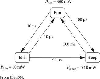
The power state machine of the SA-1100 [Ben00] has three states:
The sleep mode saves over three orders of magnitude of power consumption. However, the time required to reenter run mode from sleep is over a tenth of a second.
The SA-1100 has a companion chip, the SA-1111, that provides an integrated set of peripherals. That chip has its own power management modes that complement the SA-1100.
3.8 Design Example: Data Compressor
Our design example for this chapter is a data compressor that takes in data with a constant number of bits per data element and puts out a compressed data stream in which the data is encoded in variable-length symbols. Because this chapter concentrates on CPUs, we focus on the data compression routine itself.
3.8.1 Requirements and Algorithm
We use the Huffman coding technique, which is introduced in Application Example 3.4. We require some understanding of how our compression code fits into a larger system. Figure 3.20 shows a collaboration diagram for the data compression process. The data compressor takes in a sequence of input symbols and then produces a stream of output symbols. Assume for simplicity that the input symbols are one byte in length. The output symbols are variable length, so we have to choose a format in which to deliver the output data. Delivering each coded symbol separately is tedious, because we would have to supply the length of each symbol and use external code to pack them into words. On the other hand, bit-by-bit delivery is almost certainly too slow. Therefore, we will rely on the data compressor to pack the coded symbols into an array. There is not a one-to-one relationship between the input and output symbols, and we may have to wait for several input symbols before a packed output word comes out.
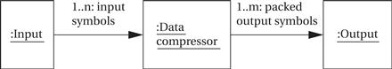
Figure 3.20 UML collaboration diagram for the data compressor.
Application Example 3.4 Huffman Coding for Text Compression
Text compression algorithms aim at statistical reductions in the volume of data. One commonly used compression algorithm is Huffman coding [Huf52], which makes use of information on the frequency of characters to assign variable-length codes to characters. If shorter bit sequences are used to identify more frequent characters, then the length of the total sequence will be reduced.
In order to be able to decode the incoming bit string, the code characters must have unique prefixes: No code may be a prefix of a longer code for another character. As a simple example of Huffman coding, assume that these characters have the following probabilities P of appearance in a message:
| Character | P |
| a | 0.45 |
| b | 0.24 |
| c | 0.11 |
| d | 0.08 |
| e | 0.07 |
| f | 0.05 |
We build the code from the bottom up. After sorting the characters by probability, we create a new symbol by adding a bit. We then compute the joint probability of finding either one of those characters and re-sort the table. The result is a tree that we can read top down to find the character codes. Here is the coding tree for our example:
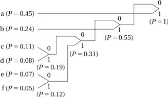
Reading the codes off the tree from the root to the leaves, we obtain the following coding of the characters:
| Character | Code |
| a | 1 |
| b | 01 |
| c | 0000 |
| d | 0001 |
| e | 0010 |
| f | 0011 |
Once the code has been constructed, which in many applications is done off-line, the codes can be stored in a table for encoding. This makes encoding simple, but clearly the encoded bit rate can vary significantly depending on the input character sequence. On the decoding side, because we do not know a priori the length of a character’s bit sequence, the computation time required to decode a character can vary significantly.
The data compressor as discussed above is not a complete system, but we can create at least a partial requirements list for the module as seen below. We used the abbreviation N/A for not applicable to describe some items that don’t make sense for a code module.
| Name | Data compression module |
| Purpose | Code module for Huffman data compression |
| Inputs | Encoding table, uncoded byte-size input symbols |
| Outputs | Packed compressed output symbols |
| Functions | Huffman coding |
| Performance | Requires fast performance |
| Manufacturing cost | N/A |
| Power | N/A |
| Physical size and weight | N/A |
3.8.2 Specification
Let’s refine the description of Figure 3.20 to come up with a more complete specification for our data compression module. That collaboration diagram concentrates on the steady-state behavior of the system. For a fully functional system, we have to provide some additional behavior:
• We have to be able to provide the compressor with a new symbol table.
• We should be able to flush the symbol buffer to cause the system to release all pending symbols that have been partially packed. We may want to do this when we change the symbol table or in the middle of an encoding session to keep a transmitter busy.
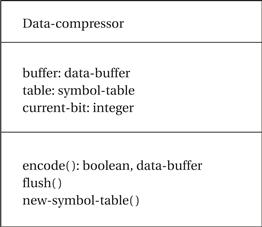
Figure 3.21 Definition of the data-compressor class.
A class description for this refined understanding of the requirements on the module is shown in Figure 3.21. The class’s buffer and current-bit behaviors keep track of the state of the encoding, and the table attribute provides the current symbol table. The class has three methods as follows:
• encode performs the basic encoding function. It takes in a one-byte input symbol and returns two values: a boolean showing whether it is returning a full buffer and, if the boolean is true, the full buffer itself.
• new-symbol-table installs a new symbol table into the object and throws away the current contents of the internal buffer.
• flush returns the current state of the buffer, including the number of valid bits in the buffer.
We also need to define classes for the data buffer and the symbol table. These classes are shown in Figure 3.22. The data-buffer will be used to hold both packed symbols and unpacked ones (such as in the symbol table). It defines the buffer itself and the length of the buffer. We have to define a data type because the longest encoded symbol is longer than an input symbol. The longest Huffman code for an eight-bit input symbol is 256 bits. (Ending up with a symbol this long happens only when the symbol probabilities have the proper values.) The insert function packs a new symbol into the upper bits of the buffer; it also puts the remaining bits in a new buffer if the current buffer is overflowed. The Symbol-table class indexes the encoded version of each symbol. The class defines an access behavior for the table; it also defines a load behavior to create a new symbol table. The relationships between these classes are shown in Figure 3.23—a data compressor object includes one buffer and one symbol table.
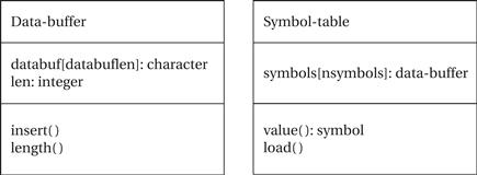
Figure 3.22 Additional class definitions for the data compressor.
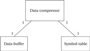
Figure 3.23 Relationships between classes in the data compressor.
Figure 3.24 shows a state diagram for the encode behavior. It shows that most of the effort goes into filling the buffers with variable-length symbols. Figure 3.25 shows a state diagram for insert. It shows that we must consider two cases—the new symbol does not fill the current buffer or it does.
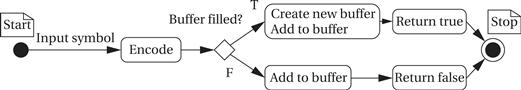
Figure 3.24 State diagram for encode behavior.
3.8.3 Program Design
Because we are only building an encoder, the program is fairly simple. We will use this as an opportunity to compare object-oriented and non-OO implementations by coding the design in both C++ and C.
OO design in C++
First is the object-oriented design using C++, because this implementation most closely mirrors the specification.
The first step is to design the data buffer. The data buffer needs to be as long as the longest symbol. We also need to implement a function that lets us merge in another data_buffer, shifting the incoming buffer by the proper amount.
const int databuflen = 8; /* as long in bytes as longest symbol */
const int bitsperbyte = 8; /* definition of byte */
const int bytemask = 0xff; /* use to mask to 8 bits for safety */
const char lowbitsmask[bitsperbyte] = { 0, 1, 3, 7, 15, 31, 63, 127}; /* used to keep low bits in a byte */
typedef char boolean; /* for clarity */
#define TRUE 1
#define FALSE 0
class data_buffer {
char databuf[databuflen] ;
int len;
int length_in_chars() { return len/bitsperbyte; } /* length inbytes rounded down--used in implementation */
public:
void insert(data_buffer, data_buffer&);
int length() { return len; } /* returns number of bits insymbol */
int length_in_bytes() { return (int)ceil(len/8.0); }
void initialize(); /* initializes the data structure */
void data_buffer::fill(data_buffer, int); /* puts upper bits
of symbol into buffer */
void operator = (data_buffer&); /* assignment operator */
data_buffer() { initialize(); } /* C++ constructor */
~data_buffer() { } /* C++ destructor */
};
data_buffer empty_buffer; /* use this to initialize other data_buffers */
void data_buffer::insert(data_buffer newval, data_buffer& newbuf) {
/* This function puts the lower bits of a symbol (newval)
into an existing buffer without overflowing the buffer. Puts
spillover, if any, into newbuf. */
int i, j, bitstoshift, maxbyte;
/* precalculate number of positions to shift up */
bitstoshift = length() – length_in_bytes()*bitsperbyte;
/* compute how many bytes to transfer--can’t run past end
of this buffer */
maxbyte = newval.length() + length() > databuflen*bitsperbyte ?
databuflen : newval.length_in_chars();
for (i = 0; i < maxbyte; i++) {
/* add lower bits of this newval byte */
databuf[i + length_in_chars()] |= (newval.databuf[i] << bitstoshift) & bytemask;
/* add upper bits of this newval byte */
databuf[i + length_in_chars() + 1] |= (newval.databuf[i] >> (bitsperbyte – bitstoshift)) & lowbitsmask[bitsperbyte – bitstoshift];
}
/* fill up new buffer if necessary */
if (newval.length() + length() > databuflen*bitsperbyte) {
/* precalculate number of positions to shift down */
bitstoshift = length() % bitsperbyte;
for (i = maxbyte, j = 0; i++, j++; i < = newval.length_in_chars()) {
newbuf.databuf[j] = (newval.databuf[i] >> bitstoshift) & bytemask;
newbuf.databuf[j] |= newval.databuf[i + 1] & lowbitsmask[bitstoshift];
}
}
/* update length */
len = len + newval.length() > databuflen*bitsperbyte ? databuflen*bitsperbyte : len + newval.length();
}
data_buffer& data_buffer::operator=(data_buffer& e) {
/* assignment operator for data buffer */
int i;
/* copy the buffer itself */
for (i = 0; i < databuflen; i++)
databuf[i] = e.databuf[i];
/* set length */
len = e.len;
/* return */
return e;
}
void data_buffer::fill(data_buffer newval, int shiftamt) {
/* This function puts the upper bits of a symbol (newval) into
the buffer. */
int i, bitstoshift, maxbyte;
/* precalculate number of positions to shift up */
bitstoshift = length() – length_in_bytes()*bitsperbyte;
/* compute how many bytes to transfer--can’t run past end
of this buffer */
maxbyte = newval.length_in_chars() > databuflen ? databuflen : newval.length_in_chars();
for (i = 0; i < maxbyte; i++) {
/* add lower bits of this newval byte */
databuf[i + length_in_chars()] = newval.databuf[i] << bitstoshift;
/* add upper bits of this newval byte */
databuf[i + length_in_chars() + 1] = newval.databuf[i] >> (bitsperbyte – bitstoshift);
}
}
void data_buffer::initialize() {
/* Initialization code for data_buffer. */
int i;
/* initialize buffer to all zero bits */
for (i = 0; i < databuflen; i++)
databuf[i] = 0;
/* initialize length to zero */
len = 0;
}
The code for data_buffer is relatively complex, and not all of its complexity was reflected in the state diagram of Figure 3.25. That doesn’t mean the specification was bad, but only that it was written at a higher level of abstraction.
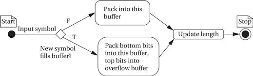
Figure 3.25 State diagram for insert behavior.
The symbol table code can be implemented relatively easily:
const int nsymbols = 256;
class symbol_table {
data_buffer symbols[nsymbols];
public:
data_buffer* value(int i) { return &(symbols[i]); }
void load(symbol_table&);
symbol_table() { } /* C++ constructor */
~symbol_table() { } /* C++ destructor */
};
void symbol_table::load(symbol_table& newsyms) {
int i;
for (i = 0; i < nsymbols; i++) {
symbols[i] = newsyms.symbols[i];
}
}
Now let’s create the class definition for data_compressor:
typedef char boolean; /* for clarity */
class data_compressor {
data_buffer buffer;
int current_bit;
symbol_table table;
public:
boolean encode(char, data_buffer&);
void new_symbol_table(symbol_table newtable)
{ table = newtable; current_bit = 0;
buffer = empty_buffer; }
int flush(data_buffer& buf)
{ int temp = current_bit; buf = buffer;
buffer = empty_buffer; current_bit = 0; return temp; }
data_compressor() { } /* C++ constructor */
~data_compressor() { } /* C++ destructor */
};
Now let’s implement the encode() method. The main challenge here is managing the buffer.
boolean data_compressor::encode(char isymbol, data_buffer& fullbuf) {
data_buffer temp;
int overlen;
/* look up the new symbol */
temp = *(table.value(isymbol)); /* the symbol itself */
/* will this symbol overflow the buffer? */
overlen = temp.length() + current_bit – buffer.length(); /*amount of overflow */
if (overlen > 0) { /* we did in fact overflow */
data_buffer nextbuf;
buffer.insert(temp,nextbuf);
/* return the full buffer and keep the next partial buffer */
fullbuf = buffer;
buffer = nextbuf;
return TRUE;
} else { /* no overflow */
data_buffer no_overflow;
buffer.insert(temp,no_overflow); /* won’t use this argument */
if (current_bit == buffer.length()) { /* return current buffer */
fullbuf = buffer;
buffer.initialize(); /* initialize the buffer */
return TRUE;
}
else return FALSE; /* buffer isn’t full yet */
}
}
Non–object-oriented implementation
We may not have the luxury of coding the algorithm in C++. While C is almost universally supported on embedded processors, support for languages that support object orientation such as C++ or Java is not so universal. How would we have to structure C code to provide multiple instantiations of the data compressor? If we want to strictly adhere to the specification, we must be able to run several simultaneous compressors, because in the object-oriented specification we can create as many new data-compressor objects as we want. To be able to run multiple data compressors simultaneously, we cannot rely on any global variables—all of the object state must be replicable. We can do this relatively easily, making the code only a little more cumbersome. We create a structure that holds the data part of the object as follows:
struct data_compressor_struct {
data_buffer buffer;
int current_bit;
sym_table table;
}
typedef struct data_compressor_struct data_compressor,
*data_compressor_ptr; /* data type declaration for convenience */
We would, of course, have to do something similar for the other classes. Depending on how strict we want to be, we may want to define data access functions to get to fields in the various structures we create. C would permit us to get to those struct fields without using the access functions, but using the access functions would give us a little extra freedom to modify the structure definitions later.
We then implement the class methods as C functions, passing in a pointer to the data_compressor object we want to operate on. Appearing below is the beginning of the modified encode method showing how we make explicit all references to the data in the object.
typedef char boolean; /* for clarity */
#define TRUE 1
#define FALSE 0
boolean data_compressor_encode(data_compressor_ptr mycmprs,
char isymbol, data_buffer *fullbuf) {
data_buffer temp;
int len, overlen;
/* look up the new symbol */
temp = mycmprs->table[isymbol].value; /* the symbol itself */
len = mycmprs->table[isymbol].length; /* its value */
…
(For C++ afficionados, the above amounts to making explicit the C++ this pointer.)
If, on the other hand, we didn’t care about the ability to run multiple compressions simultaneously, we can make the functions a little more readable by using global variables for the class variables:
static data_buffer buffer;
static int current_bit;
static sym_table table;
We have used the C static declaration to ensure that these globals are not defined outside the file in which they are defined; this gives us a little added modularity. We would, of course, have to update the specification so that it makes clear that only one compressor object can be running at a time. The functions that implement the methods can then operate directly on the globals as seen below.
boolean data_compressor_encode(char isymbol,
data_buffer& fullbuf){
data_buffer temp;
int len, overlen;
/* look up the new symbol */
temp = table[isymbol].value; /* the symbol itself */
len = table[isymbol].length; /* its value */
…
Notice that this code does not need the structure pointer argument, making it resemble the C++ code a little more closely. However, horrible bugs will ensue if we try to run two different compressions at the same time through this code.
What can we say about the efficiency of this code? Efficiency has many aspects covered in more detail in Chapter 5. For the moment, let’s consider instruction selection, that is, how well the compiler does in choosing the right instructions to implement the operations. Bit manipulations such as we do here often raise concerns about efficiency. But if we have a good compiler and we select the right data types, instruction selection is usually not a problem. If we use data types that don’t require data type transformations, a good compiler can select the right instructions to efficiently implement the required operations.
3.8.4 Testing
How do we test this program module to be sure it works? We consider testing much more thoroughly in Section 5.11. In the meantime, we can use common sense to come up with some testing techniques.
One way to test the code is to run it and look at the output without considering how the code is written. In this case, we can load up a symbol table, run some symbols through it, and see whether we get the correct result. We can get the symbol table from outside sources or by writing a small program to generate it ourselves. We should test several different symbol tables. We can get an idea of how thoroughly we are covering the possibilities by looking at the encoding trees—if we choose several very different looking encoding trees, we are likely to cover more of the functionality of the module. We also want to test enough symbols for each symbol table. One way to help automate testing is to write a Huffman decoder. As illustrated in Figure 3.26, we can run a set of symbols through the encoder, and then through the decoder, and simply make sure that the input and output are the same. If they are not, we have to check both the encoder and decoder to locate the problem, but because most practical systems will require both in any case, this is a minor concern.
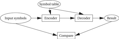
Figure 3.26 A test of the encoder.
Another way to test the code is to examine the code itself and try to identify potential problem areas. When we read the code, we should look for places where data operations take place to see that they are performed properly. We also want to look at the conditionals to identify different cases that need to be exercised. Here are some of the issues that we need to consider in testing:
• Is it possible to run past the end of the symbol table?
• What happens when the next symbol does not fill up the buffer?
• What happens when the next symbol exactly fills up the buffer?
• What happens when the next symbol overflows the buffer?
• Do very long encoded symbols work properly? How about very short ones?
Testing the internals of code often requires building scaffolding code. For example, we may want to test the insert method separately, which would require building a program that calls the method with the proper values. If our programming language comes with an interpreter, building such scaffolding is easier because we don’t have to create a complete executable, but we often want to automate such tests even with interpreters because we will usually execute them several times.
3.9 Summary
Numerous mechanisms must be used to implement complete computer systems. For example, interrupts have little direct visibility in the instruction set, but they are very important to input and output operations. Similarly, memory management is invisible to most of the program but is very important to creating a working system.
Although we are not directly concerned with the details of computer architecture, characteristics of the underlying CPU hardware have a major impact on programs. When designing embedded systems, we are typically concerned about characteristics such as execution speed or power consumption. Having some understanding of the factors that determine performance and power will help you later as you develop techniques for optimizing programs to meet these criteria.
What we Learned
• The two major styles of I/O are polled and interrupt driven.
• Interrupts may be vectorized and prioritized.
• Supervisor mode helps protect the computer from program errors and provides a mechanism for controlling multiple programs.
• An exception is an internal error; a trap or software interrupt is explicitly generated by an instruction. Both are handled similarly to interrupts.
• A cache provides fast storage for a small number of main memory locations. Caches may be direct mapped or set associative.
• A memory management unit translates addresses from logical to physical addresses.
• Co-processors provide a way to optionally implement certain instructions in hardware.
• Program performance can be influenced by pipelining, superscalar execution, and the cache. Of these, the cache introduces the most variability into instruction execution time.
• CPUs may provide static (independent of program behavior) or dynamic (influenced by currently executing instructions) methods for managing power consumption.
Further reading
As with instruction sets, the ARM and C55x manuals provide good descriptions of exceptions, memory management, and caches for those processors. Patterson and Hennessy [Pat98] provide a thorough description of computer architecture, including pipelining, caches, and memory management.
Questions
Q3-1 Why do most computer systems use memory-mapped I/O?
Q3-2 Why do most programs use interrupt-driven I/O over busy/wait?
Q3-3 Write ARM code that tests a register at location ds1 and continues execution only when the register is nonzero.
Q3-4 Write ARM code that waits for the low-order bit of device register ds1 to become 1 and then reads a value from register dd1.
Q3-5 Implement peek() and poke() in assembly language for ARM.
Q3-6 Draw a UML sequence diagram for a busy-wait read of a device. The diagram should include the program running on the CPU and the device.
Q3-7 Draw a UML sequence diagram for a busy-wait write of a device. The diagram should include the program running on the CPU and the device.
Q3-8 Draw a UML sequence diagram for copying characters from an input to an output device using busy-wait I/O. The diagram should include the two devices and the two busy-wait I/O handlers.
Q3-9 When would you prefer to use busy-wait I/O over interrupt-driven I/O?
Q3-10 If you could only have one of vectors or priorities in your interrupt system, which would you rather have?
Q3-11 Draw a UML sequence diagram for an interrupt-driven read of a device. The diagram should include the background program, the handler, and the device.
Q3-12 Draw a UML sequence diagram for an interrupt-driven write of a device. The diagram should include the background program, the handler, and the device.
Q3-13 Draw a UML sequence diagram for a vectored interrupt-driven read of a device. The diagram should include the background program, the interrupt vector table, the handler, and the device.
Q3-14 Draw a UML sequence diagram for copying characters from an input to an output device using interrupt-driven I/O. The diagram should include the two devices and the two I/O handlers.
Q3-15 Draw a UML sequence diagram of a higher-priority interrupt that happens during a lower-priority interrupt handler. The diagram should include the device, the two handlers, and the background program.
Q3-16 Draw a UML sequence diagram of a lower-priority interrupt that happens during a higher-priority interrupt handler. The diagram should include the device, the two handlers, and the background program.
Q3-17 Draw a UML sequence diagram of a nonmaskable interrupt that happens during a low-priority interrupt handler. The diagram should include the device, the two handlers, and the background program.
Q3-18 Draw a UML state diagram for the steps performed by an ARM7 when it responds to an interrupt.
Q3-19 Three devices are attached to a microprocessor: Device 1 has highest priority and device 3 has lowest priority. Each device’s interrupt handler takes 5 time units to execute. Show what interrupt handler (if any) is executing at each time given the sequence of device interrupts displayed below.
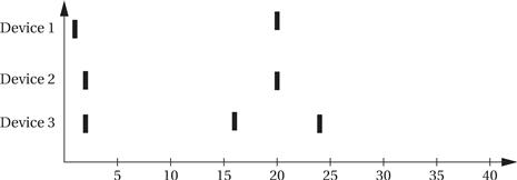
Q3-20 Draw a UML sequence diagram that shows how an ARM processor goes into supervisor mode. The diagram should include the supervisor mode program and the user mode program.
Q3-21 Give three examples of typical types of exceptions handled by CPUs.
Q3-22 What are traps used for?
Q3-23 Draw a UML sequence diagram that shows how an ARM processor handles a floating-point exception. The diagram should include the user program, the exception handler, and the exception handler table.
Q3-24 Provide examples of how each of the following can occur in a typical program:
Q3-25 What is the average memory access time of a machine whose hit rate is 96%, with a cache access time of 3 ns and a main memory access time of 70 ns?
Q3-26 If we want an average memory access time of 6.5 ns, our cache access time is 5 ns, and our main memory access time is 80 ns, what cache hit rate must we achieve?
Q3-27 In the two-way, set-associative cache with four banks of Example 3.8, show the state of the cache after each memory access, as was done for the direct-mapped cache. Use an LRU replacement policy.
Q3-28 The following code is executed by an ARM processor with each instruction executed exactly once:
MOV r0,#0 ; use r0 for i, set to 0
LDR r1,#10 ; get value of N for loop termination test
MOV r2,#0 ; use r2 for f, set to 0
ADR r3,c ; load r3 with address of base of c array
ADR r5,x ; load r5 with address of base of x array
; loop test
loop CMP r0,r1
BGE loopend ; if i >= N, exit loop
; loop body
LDR r4,[r3,r0] ; get value of c[i]
LDR r6,[r5,r0] ; get value of x[i]
MUL r4,r4,r6 ; compute c[i]*x[i]
ADD r2,r2,r4 ; add into running sum f
; update loop counter
ADD r0,r0,#1 ; add 1 to i
B loop ; unconditional branch to top of loop
Show the contents of the instruction cache for these configurations, assuming each line holds one ARM instruction:
Q3-29 Show a UML state diagram for a paged address translation using a flat page table.
Q3-30 Show a UML state diagram for a paged address translation using a three-level, tree-structured page table.
Q3-31 What are the stages in an ARM pipeline?
Q3-32 What are the stages in the C55x pipeline?
Q3-33 What is the difference between latency and throughput?
Q3-34 Draw a pipeline diagram for an ARM7 pipeline’s execution of three fictional instructions: aa, bb, and cc. The aa instruction always requires two cycles to complete the execute stage. The cc instruction takes two cycles to complete the execute stage if the previous instruction was a bb instruction. Draw the pipeline diagram for these sequence of instructions:
Q3-35 Draw two pipeline diagrams showing what happens when an ARM BZ instruction is taken and not taken, respectively.
Q3-36 Name three mechanisms by which a CMOS microprocessor consumes power.
Q3-37 Provide a user-level example of
Q3-38 Why can’t you use the same mechanism to return from a sleep power-saving state as you do from an idle power-saving state?
Lab exercises
L3-1 Write a simple loop that lets you exercise the cache. By changing the number of statements in the loop body, you can vary the cache hit rate of the loop as it executes. If your microprocessor fetches instructions from off-chip memory, you should be able to observe changes in the speed of execution by observing the microprocessor bus.
L3-2 If your CPU has a pipeline that gives different execution times when a branch is taken or not taken, write a program in which these branches take different amounts of time. Use a CPU simulator to observe the behavior of the program.
L3-3 Measure the time required to respond to an interrupt.